temperature effects and transport phenomena … 2011_tcm18-431… · temperature effects and...
TRANSCRIPT
TEMPERATURE EFFECTS AND TRANSPORT PHENOMENA INTERAHERTZ QUANTUM CASCADE LASERS
BY
PHILIP C. SLINGERLANDB.A.(2004)
SUBMITTED IN PARTIAL FULFILLMENT OF THE REQUIREMENTSFOR THE DEGREE OF DOCTOR OF PHILOSOPHY
DEPARTMENT OF PHYSICSUNIVERSITY OF MASSACHUSETTS LOWELL
Signature of Author
Signature of Dissertation Chair: Dr. Christopher S. Baird
Signatures of Dissertation Committee Members:
Dr. Robert H. Giles
Dr. Viktor A. Podolskiy
TEMPERATURE EFFECTS AND TRANSPORT PHENOMENA INTERAHERTZ QUANTUM CASCADE LASERS
BY
PHILIP C. SLINGERLAND
ABSTRACT OF A DISSERTATION SUBMITTED TO THE FACULTY OFDEPARTMENT OF PHYSICS
IN PARTIAL FULFILLMENT OF THE REQUIREMENTSFOR THE DEGREE OF
DOCTOR OF PHILOSOPHYPHYSICS
UNIVERSITY OF MASSACHUSETTS LOWELL2011
Dissertation Supervisor: Dr. Christopher S. Baird
Abstract
Quantum cascade lasers (QCL’s) employ the mid- and far-infrared intersubband ra-
diative transitions available in semiconductor heterostructures. Through the precise
design and construction of these heterostructures the laser characteristics and out-
put frequencies can be controlled. When fabricated, QCL’s offer a lightweight and
portable alternative to traditional laser systems which emit in this frequency range.
The successful operation of these devices strongly depends on the effects of electron
transport. Studies have been conducted on the mechanisms involved in electron trans-
port and a computational model has been completed for QCL performance prediction
and design optimization. The implemented approach utilized a three period model
of the laser active region with periodic boundary conditions enforced. All of the
wavefunctions within these periods were included in a self-consistent rate equation
model. This model employed all relevant types of scattering mechanisms within three
periods. Additionally, an energy balance equation was studied to determine the set
of individual subband electron temperatures. This equation included the influence
of both electron-LO phonon and electron-electron scattering. The effect of differ-
ent modeling parameters within QCL electron temperature predictions are presented
along with a description of the complete QCL computational model and comparisons
with experimental results.
ii
Acknowledgements
I would like to thank Christopher Baird for giving me the opportunity to study with
him. He is an outstanding advisor and, more importantly, a great teacher. All of the
progress that I made would not have been possible without his ability to explain the
often frustrating physics of quantum cascade lasers.
I would also like to thank the faculty and staff at both The Submillimeter-wave
Technology Laboratory and The Photonics Center at the University of Massachusetts
Lowell. My work owes its birth to the ongoing research of source technologies at
these facilities. In particular, I am grateful for the generous support of both Robert
Giles and William Goodhue who provided funding and resources for the duration
of my PhD. Additionally, I am grateful to Xifeng Qian and Shiva Vangala for their
many marathon growth campaigns, Neelima Chandrayan for her skilled processing of
samples, and Andriy Danylov for his pain-staking characterization of devices. And
of course, I am grateful to all the other colleagues who answered my questions both
during the writing of this thesis and throughout my research.
I must also thank all my friends and family members who were so patient and
understanding during my graduate studies. Lastly, I would like to thank my wife,
Elizabeth. Her constant support and encouragement has inspired me to do more than
I ever could have without her.
iii

for Elizabeth
iv
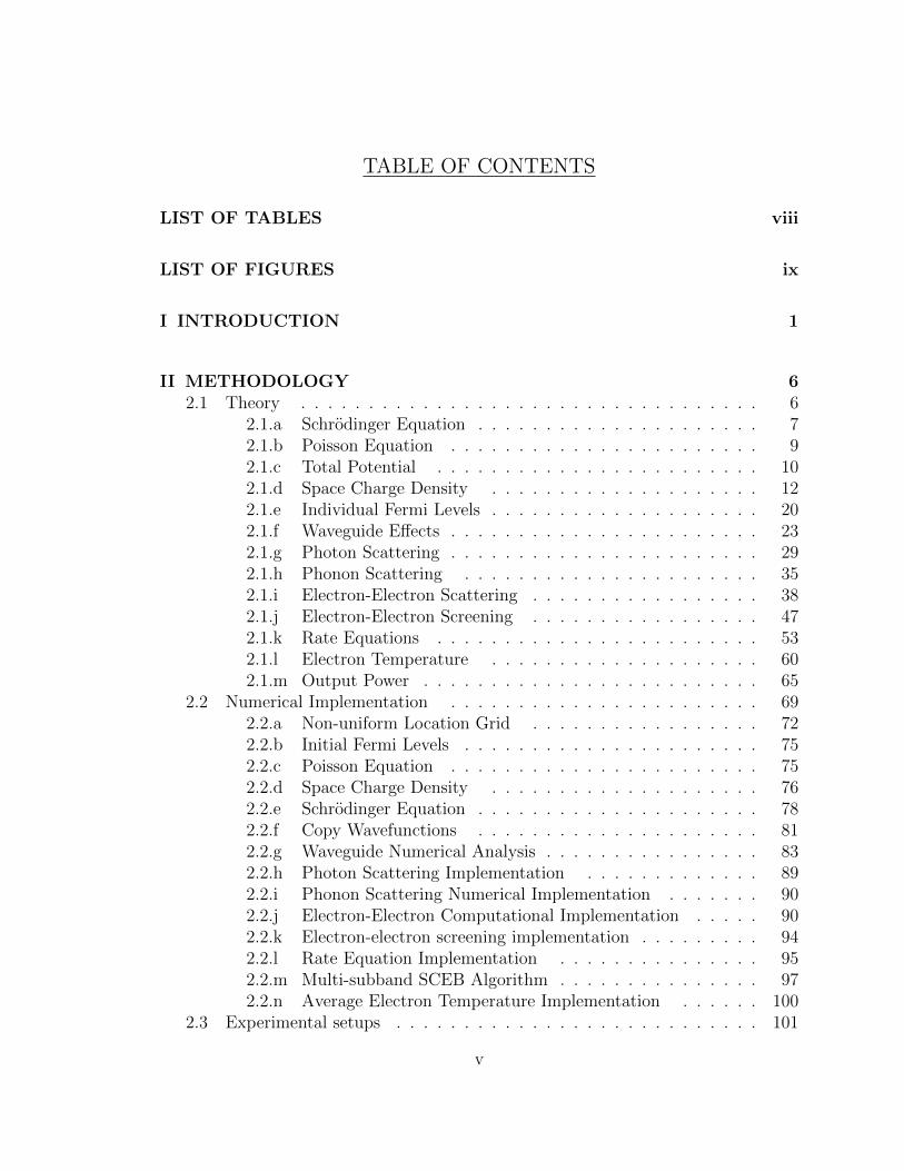
TABLE OF CONTENTS
LIST OF TABLES viii
LIST OF FIGURES ix
I INTRODUCTION 1
II METHODOLOGY 62.1 Theory . . . . . . . . . . . . . . . . . . . . . . . . . . . . . . . . . . 6
2.1.a Schrodinger Equation . . . . . . . . . . . . . . . . . . . . . 72.1.b Poisson Equation . . . . . . . . . . . . . . . . . . . . . . . 92.1.c Total Potential . . . . . . . . . . . . . . . . . . . . . . . . 102.1.d Space Charge Density . . . . . . . . . . . . . . . . . . . . 122.1.e Individual Fermi Levels . . . . . . . . . . . . . . . . . . . . 202.1.f Waveguide Effects . . . . . . . . . . . . . . . . . . . . . . . 232.1.g Photon Scattering . . . . . . . . . . . . . . . . . . . . . . . 292.1.h Phonon Scattering . . . . . . . . . . . . . . . . . . . . . . 352.1.i Electron-Electron Scattering . . . . . . . . . . . . . . . . . 382.1.j Electron-Electron Screening . . . . . . . . . . . . . . . . . 472.1.k Rate Equations . . . . . . . . . . . . . . . . . . . . . . . . 532.1.l Electron Temperature . . . . . . . . . . . . . . . . . . . . 602.1.m Output Power . . . . . . . . . . . . . . . . . . . . . . . . . 65
2.2 Numerical Implementation . . . . . . . . . . . . . . . . . . . . . . . 692.2.a Non-uniform Location Grid . . . . . . . . . . . . . . . . . 722.2.b Initial Fermi Levels . . . . . . . . . . . . . . . . . . . . . . 752.2.c Poisson Equation . . . . . . . . . . . . . . . . . . . . . . . 752.2.d Space Charge Density . . . . . . . . . . . . . . . . . . . . 762.2.e Schrodinger Equation . . . . . . . . . . . . . . . . . . . . . 782.2.f Copy Wavefunctions . . . . . . . . . . . . . . . . . . . . . 812.2.g Waveguide Numerical Analysis . . . . . . . . . . . . . . . . 832.2.h Photon Scattering Implementation . . . . . . . . . . . . . 892.2.i Phonon Scattering Numerical Implementation . . . . . . . 902.2.j Electron-Electron Computational Implementation . . . . . 902.2.k Electron-electron screening implementation . . . . . . . . . 942.2.l Rate Equation Implementation . . . . . . . . . . . . . . . 952.2.m Multi-subband SCEB Algorithm . . . . . . . . . . . . . . . 972.2.n Average Electron Temperature Implementation . . . . . . 100
2.3 Experimental setups . . . . . . . . . . . . . . . . . . . . . . . . . . . 101
v

2.3.a QCL production methods . . . . . . . . . . . . . . . . . . 1022.3.b Device characterization methods . . . . . . . . . . . . . . . 1052.3.c Details of grown devices . . . . . . . . . . . . . . . . . . . 106
III RESULTS 1103.1 Average Electron Temperature . . . . . . . . . . . . . . . . . . . . . 1103.2 The effect of approximations on e-e scattering rates . . . . . . . . . . 114
3.2.a Convergence and integration types . . . . . . . . . . . . . . 1183.2.b State-blocking and screening . . . . . . . . . . . . . . . . . 1193.2.c Symmetric and asymmetric transitions . . . . . . . . . . . . 123
3.3 Scaling Studies . . . . . . . . . . . . . . . . . . . . . . . . . . . . . . 1263.4 Screening Studies . . . . . . . . . . . . . . . . . . . . . . . . . . . . . 1283.5 Multi-subband electron temperature model . . . . . . . . . . . . . . 129
3.5.a 3.4 THz, three-well design . . . . . . . . . . . . . . . . . . . 1293.5.b 2.8 THz, four-well design . . . . . . . . . . . . . . . . . . . 131
3.6 Temperature optimization . . . . . . . . . . . . . . . . . . . . . . . . 133
IV DISCUSSIONS 1364.1 Average Electron Temperature . . . . . . . . . . . . . . . . . . . . . 1364.2 The effect of approximations on e-e scattering rates . . . . . . . . . . 138
4.2.a Convergence and integration types . . . . . . . . . . . . . . 1384.2.b State-blocking and screening . . . . . . . . . . . . . . . . . 1394.2.c Symmetric and asymmetric transitions . . . . . . . . . . . . 140
4.3 Scaling Studies . . . . . . . . . . . . . . . . . . . . . . . . . . . . . . 1414.4 Screening Studies . . . . . . . . . . . . . . . . . . . . . . . . . . . . . 1424.5 Multi-subband electron temperature model . . . . . . . . . . . . . . 143
4.5.a 3.4 THz, three-well design . . . . . . . . . . . . . . . . . . . 1434.5.b 2.8 THz, four-well design . . . . . . . . . . . . . . . . . . . 144
4.6 Temperature optimization . . . . . . . . . . . . . . . . . . . . . . . . 145
V CONCLUSIONS 1465.1 Average Electron Temperature Calculations . . . . . . . . . . . . . . 1465.2 Electron-electron scattering rate approximations . . . . . . . . . . . . 1465.3 Device scaling . . . . . . . . . . . . . . . . . . . . . . . . . . . . . . . 1475.4 Electron-electron screening . . . . . . . . . . . . . . . . . . . . . . . . 1475.5 Multi-subband energy balance model . . . . . . . . . . . . . . . . . . 1485.6 Temperature optimization . . . . . . . . . . . . . . . . . . . . . . . . 148
vi

VI RECOMMENDATIONS 150
VII REFERENCES 151
VIII BIOGRAPHY 160
vii
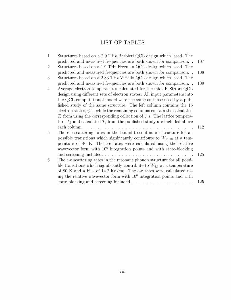
LIST OF TABLES
1 Structures based on a 2.9 THz Barbieri QCL design which lased. Thepredicted and measured frequencies are both shown for comparison. . 107
2 Structures based on a 1.9 THz Freeman QCL design which lased. Thepredicted and measured frequencies are both shown for comparison. . 108
3 Structures based on a 2.83 THz Vitiello QCL design which lased. Thepredicted and measured frequencies are both shown for comparison. . 109
4 Average electron temperatures calculated for the mid-IR Sirtori QCLdesign using different sets of electron states. All input parameters intothe QCL computational model were the same as those used by a pub-lished study of the same structure. The left column contains the 15electron states, ψ’s, while the remaining columns contain the calculatedTe from using the corresponding collection of ψ’s. The lattice tempera-ture TL and calculated Te from the published study are included aboveeach column. . . . . . . . . . . . . . . . . . . . . . . . . . . . . . . . 112
5 The e-e scattering rates in the bound-to-continuum structure for allpossible transitions which significantly contribute to W11,10 at a tem-perature of 40 K. The e-e rates were calculated using the relativewavevector form with 106 integration points and with state-blockingand screening included. . . . . . . . . . . . . . . . . . . . . . . . . . . 125
6 The e-e scattering rates in the resonant phonon structure for all possi-ble transitions which significantly contribute to W4,3 at a temperatureof 80 K and a bias of 14.2 kV/cm. The e-e rates were calculated us-ing the relative wavevector form with 106 integration points and withstate-blocking and screening included. . . . . . . . . . . . . . . . . . . 125
viii
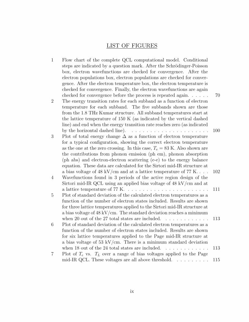
LIST OF FIGURES
1 Flow chart of the complete QCL computational model. Conditionalsteps are indicated by a question mark. After the Schrodinger-Poissonbox, electron wavefunctions are checked for convergence. After theelectron populations box, electron populations are checked for conver-gence. After the electron temperature box, the electron temperature ischecked for convergence. Finally, the electron wavefunctions are againchecked for convergence before the process is repeated again. . . . . . 70
2 The energy transition rates for each subband as a function of electrontemperature for each subband. The five subbands shown are thosefrom the 1.8 THz Kumar structure. All subband temperatures start atthe lattice temperature of 150 K (as indicated by the vertical dashedline) and end when the energy transition rate reaches zero (as indicatedby the horizontal dashed line). . . . . . . . . . . . . . . . . . . . . . 100
3 Plot of total energy change ∆ as a function of electron temperaturefor a typical configuration, showing the correct electron temperatureas the one at the zero crossing. In this case, Te = 83 K. Also shown arethe contributions from phonon emission (ph em), phonon absorption(ph abs) and electron-electron scattering (e-e) to the energy balanceequation. These data are calculated for the Sirtori mid-IR structure ata bias voltage of 48 kV/cm and at a lattice temperature of 77 K. . . . 102
4 Wavefunctions found in 3 periods of the active region design of theSirtori mid-IR QCL using an applied bias voltage of 48 kV/cm and ata lattice temperature of 77 K. . . . . . . . . . . . . . . . . . . . . . . 111
5 Plot of standard deviation of the calculated electron temperatures as afunction of the number of electron states included. Results are shownfor three lattice temperatures applied to the Sirtori mid-IR structure ata bias voltage of 48 kV/cm. The standard deviation reaches a minimumwhen 20 out of the 27 total states are included. . . . . . . . . . . . . 113
6 Plot of standard deviation of the calculated electron temperatures as afunction of the number of electron states included. Results are shownfor six lattice temperatures applied to the Page mid-IR structure ata bias voltage of 53 kV/cm. There is a minimum standard deviationwhen 18 out of the 24 total states are included. . . . . . . . . . . . . 113
7 Plot of Te vs. TL over a range of bias voltages applied to the Pagemid-IR QCL. These voltages are all above threshold. . . . . . . . . . 115
ix
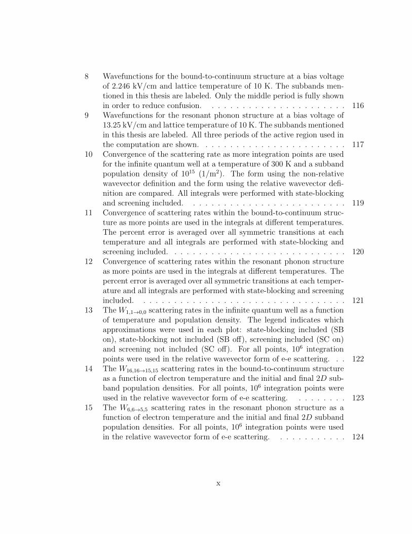
8 Wavefunctions for the bound-to-continuum structure at a bias voltageof 2.246 kV/cm and lattice temperature of 10 K. The subbands men-tioned in this thesis are labeled. Only the middle period is fully shownin order to reduce confusion. . . . . . . . . . . . . . . . . . . . . . . 116
9 Wavefunctions for the resonant phonon structure at a bias voltage of13.25 kV/cm and lattice temperature of 10 K. The subbands mentionedin this thesis are labeled. All three periods of the active region used inthe computation are shown. . . . . . . . . . . . . . . . . . . . . . . . 117
10 Convergence of the scattering rate as more integration points are usedfor the infinite quantum well at a temperature of 300 K and a subbandpopulation density of 1015 (1/m2). The form using the non-relativewavevector definition and the form using the relative wavevector defi-nition are compared. All integrals were performed with state-blockingand screening included. . . . . . . . . . . . . . . . . . . . . . . . . . 119
11 Convergence of scattering rates within the bound-to-continuum struc-ture as more points are used in the integrals at different temperatures.The percent error is averaged over all symmetric transitions at eachtemperature and all integrals are performed with state-blocking andscreening included. . . . . . . . . . . . . . . . . . . . . . . . . . . . . 120
12 Convergence of scattering rates within the resonant phonon structureas more points are used in the integrals at different temperatures. Thepercent error is averaged over all symmetric transitions at each temper-ature and all integrals are performed with state-blocking and screeningincluded. . . . . . . . . . . . . . . . . . . . . . . . . . . . . . . . . . 121
13 The W1,1→0,0 scattering rates in the infinite quantum well as a functionof temperature and population density. The legend indicates whichapproximations were used in each plot: state-blocking included (SBon), state-blocking not included (SB off), screening included (SC on)and screening not included (SC off). For all points, 106 integrationpoints were used in the relative wavevector form of e-e scattering. . . 122
14 The W16,16→15,15 scattering rates in the bound-to-continuum structureas a function of electron temperature and the initial and final 2D sub-band population densities. For all points, 106 integration points wereused in the relative wavevector form of e-e scattering. . . . . . . . . 123
15 The W6,6→5,5 scattering rates in the resonant phonon structure as afunction of electron temperature and the initial and final 2D subbandpopulation densities. For all points, 106 integration points were usedin the relative wavevector form of e-e scattering. . . . . . . . . . . . 124
x
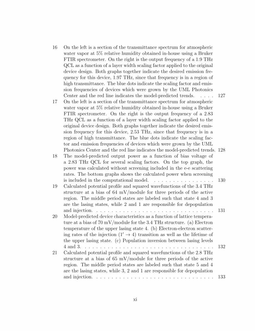
16 On the left is a section of the transmittance spectrum for atmosphericwater vapor at 5% relative humidity obtained in-house using a BrukerFTIR spectrometer. On the right is the output frequency of a 1.9 THzQCL as a function of a layer width scaling factor applied to the originaldevice design. Both graphs together indicate the desired emission fre-quency for this device, 1.97 THz, since that frequency is in a region ofhigh transmittance. The blue dots indicate the scaling factor and emis-sion frequencies of devices which were grown by the UML PhotonicsCenter and the red line indicates the model-predicted trends. . . . . 127
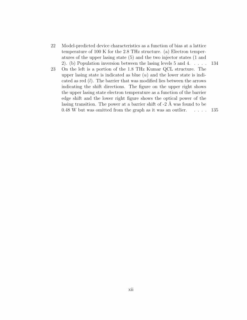
17 On the left is a section of the transmittance spectrum for atmosphericwater vapor at 5% relative humidity obtained in-house using a BrukerFTIR spectrometer. On the right is the output frequency of a 2.83THz QCL as a function of a layer width scaling factor applied to theoriginal device design. Both graphs together indicate the desired emis-sion frequency for this device, 2.53 THz, since that frequency is in aregion of high transmittance. The blue dots indicate the scaling fac-tor and emission frequencies of devices which were grown by the UMLPhotonics Center and the red line indicates the model-predicted trends. 128
18 The model-predicted output power as a function of bias voltage ofa 2.83 THz QCL for several scaling factors. On the top graph, thepower was calculated without screening included in the e-e scatteringrates. The bottom graphs shows the calculated power when screeningis included in the computational model. . . . . . . . . . . . . . . . . 130
19 Calculated potential profile and squared wavefunctions of the 3.4 THzstructure at a bias of 64 mV/module for three periods of the activeregion. The middle period states are labeled such that state 4 and 3are the lasing states, while 2 and 1 are responsible for depopulationand injection. . . . . . . . . . . . . . . . . . . . . . . . . . . . . . . . 131
20 Model-predicted device characteristics as a function of lattice tempera-ture at a bias of 70 mV/module for the 3.4 THz structure. (a) Electrontemperature of the upper lasing state 4. (b) Electron-electron scatter-ing rates of the injection (1′ → 4) transition as well as the lifetime ofthe upper lasing state. (c) Population inversion between lasing levels4 and 3. . . . . . . . . . . . . . . . . . . . . . . . . . . . . . . . . . . 132
21 Calculated potential profile and squared wavefunctions of the 2.8 THzstructure at a bias of 65 mV/module for three periods of the activeregion. The middle period states are labeled such that state 5 and 4are the lasing states, while 3, 2 and 1 are responsible for depopulationand injection. . . . . . . . . . . . . . . . . . . . . . . . . . . . . . . . 133
xi
22 Model-predicted device characteristics as a function of bias at a latticetemperature of 100 K for the 2.8 THz structure. (a) Electron temper-atures of the upper lasing state (5) and the two injector states (1 and2). (b) Population inversion between the lasing levels 5 and 4. . . . . 134
23 On the left is a portion of the 1.8 THz Kumar QCL structure. Theupper lasing state is indicated as blue (u) and the lower state is indi-cated as red (l). The barrier that was modified lies between the arrowsindicating the shift directions. The figure on the upper right showsthe upper lasing state electron temperature as a function of the barrieredge shift and the lower right figure shows the optical power of thelasing transition. The power at a barrier shift of -2 A was found to be0.48 W but was omitted from the graph as it was an outlier. . . . . 135
xii
1
I. INTRODUCTION
Terahertz (THz) radiation is a portion of the electromagnetic spectrum which
lies between the infrared and microwave frequencies and is typically defined to be
between the wavelengths of 600 to 30 µm (i.e. 0.5 - 10 THz). This region is of par-
ticular interest due to the large number of potential applications which have recently
been suggested.1,2 These applications are typically related to two characteristics of
THz radiation: its absorption by water and its transparency to dielectric materials.
This leads to uses in medical imaging, where differences in water content between
tissue types can be used to differentiate healthy from cancerous tissues;3–7 security
screening, where the transparency of clothing to terahertz radiation can allow the
imaging of concealed objects;8,9 and quality assurance, where the transparency of
paper and cardboard allows for the imaging of packaged contents.10,11 However, it
should also be noted that many other molecules aside from water have strong spec-
tral signatures at terahertz frequencies. This has led to further interest in remote
detection applications,12,13 provided that atmospheric absorption can be minimized,
and satellite based communication and spectroscopy,14,15 where atmospheric effects
are not a problem.
All of these applications would benefit greatly from a compact, coherent and
continuous-wave (cw) source of THz radiation that provides an adequate signal-to-
noise ratio for real-time imaging and allows integration into large-array detectors for
remote-sensing.16 However, development in this area has been slow. In terms of solid-
2
state devices, such as Gunn oscillators and Schottky diode multipliers, the output
power has not been able to exceed the milliwatt level above 1 THz.1,17–20 Photonic
approaches to terahertz generation are limited by the small band gaps required at
these frequencies. For example, lead salt laser diodes cannot emit at frequencies
lower than 15 THz. These frequencies can also be generated through multiplication
up from millimeter-wave sources such as optically pumped molecular gas lasers or
free-electron lasers. However, these systems are not attractive for the mentioned
applications due to their size, cost and complexity. Further discussions of the current
state and limitations of terahertz technologies can be found in the literature.21,22
Terahertz quantum cascade lasers (QCL’s) have helped to fill this gap of viable
THz sources. A QCL is a type of semiconductor laser whose emission frequency can be
chosen by proper design of the epitaxial layers. They are made by growing alternating
layers of material with varying thicknesses onto a substrate. Each layer is only a few
nanometers thick but still maintains a band-gap between the conduction and valence
bands. At the junction of the layers the difference of the conduction band energies
forms a potential barrier. These heterostructures establish a series of finite quantum
wells that confine electrons. Additionally, a bias voltage is applied which provides
electronic pumping. In each period of the active region, electrons tunnel through the
energy barriers, de-excite, emit a photon, and continue tunneling through to the next
period to repeat the process.
The first suggestion of such a device came in 1971 by Kazarinov23 after which
followed a long period of experimental investigation. However, QCL’s experienced
3
rapid development once the first successful mid-IR device was created by Faist24
and the first THz device was made by Kohler.25 Currently, QCL’s can emit at any
frequency in the THz range, but this flexibility is not matched with high power or
temperature performance. The maximum power from a THz QCL so far is 250 mW
in pulsed mode and 130 mW in cw mode, as demonstrated by Williams.26 But this
success has only been seen above 4 THz and lower frequencies see a reduction in the
optical power. Similarly, the highest operating temperature is 186 K for a 3.9 THz
laser designed by Kumar,27 but at 1.2 THz the highest operating temperature is only
69 K, as demonstrated by Walther.28 There is a need to improve their performance
if the potential applications are to be successful.
Further improvement of these devices requires a complete understanding of the
many mechanisms which affect their performance. In particular, electron-electron
(e-e) scattering is a crucial element to the operation and design of QCL’s since it con-
tributes heavily to the transport of electrons in the laser active region.29 Specifically,
the injection and depopulation of lasing states is often designed to be dependent upon
e-e scattering. This is especially true in the THz regime where the energy spacing
between states is small and, therefore, very sensitive to e-e scattering.
Also, electron heating is another important effect since all of the electron scatter-
ing rates are strongly temperature dependent. Therefore, electron or carrier transport
will by strongly affected by any increase in temperature that the electrons may ex-
perience. Due to the small energy spacing between electron energy levels, thermal
effects may be particularly harmful to the carefully designed electron populations. In
4
order for devices to operate at higher temperatures, either the electrons have to be
kept as cool as possible or the laser must be designed with electron heating in mind.
Both methods require device modeling to be performed.
Device modeling is an important element in meeting this need to improve QCL
properties and several methods exist for producing QCL predictions. One such model,
the self-consistent energy balance (SCEB) model was proposed by Harrison,30 and has
been shown to predict lasing characteristics without the computational demands of
Monte Carlo31–33 or non-equilibrium Green’s function34–38 methods. Another model,
the density-matrix model,39,40 which has been suggested as an alternative to the self-
consistent approach, has the appeal of being relatively easy to implement and with low
computational demand. However, since this model considers scattering events within
a smaller portion of the active region as compared to the self-consistent model, many
vital effects can be lost as discussed by Beji.41
An improvement to the SCEB model has been suggested by Jovanovic,42 which
determines the temperature of every subband within the QCL conduction band. Such
a model would provide a means to determine thermal effects, which have a significant
impact on the transport mechanisms within a QCL (through thermal backfilling,
parasitic transitions, etc.).
In the sections that follow, a full description of the computational model em-
ployed (based on the SCEB approach) will be given in addition to a theoretical de-
scription of the various components. Particular emphasis will be placed on electron-
electron interactions and electron heating due to the reasons mentioned above. In
5
addition, the results of these models will be presented along with experimental find-
ings, demonstrating the role thermal effects play in QCL physics.
6
II. METHODOLOGY
2.1 Theory
The QCL computational model is comprised of many components which are all based
on physical first principles wherever possible. In order to accomplish this, many
theoretical aspects had to be derived and understood so that they could be properly
implemented numerically. In the following subsections, a detailed explanation of
these various theoretical aspects can be found. In Section 2.2, a description of their
numerical implementations is also given.
First, the appropriate form of the Schrodinger and Poisson equations are derived
in the context of a conduction band heterostructure to find the electron states. Sup-
plemental information on the total potential, space charge density and Fermi levels
is also given in this context. Then, the waveguide effects are derived to help deter-
mine the fields that can exist in QCL structures. These are followed by derivations
for the three primary forms of carrier scattering discussed in this thesis: electron-
photon, electron-phonon, and electron-electron scattering. Additionally, the effect of
screening on electron-electron scattering is derived to further enhance the accuracy
of this vital particle interaction. Electron-impurity and electron-interface scattering
effects were not included. Although there has been evidence both for and against
the significance of these scattering channels,43–47 it was decided for this particular
research effort, where low-doped, THz QCL’s are involved, that the effects of impu-
7
rity and interface scattering are negligible. The rate equations, which determine the
electron populations densities, are then derived. These are followed by the energy
balance equations, which determine the electron temperatures. Finally, the necessary
equations for calculating the output properties of a QCL are given.
2.1.a Schrodinger Equation
Quantum cascade lasers are fabricated by stacking up alternating layers of semicon-
ductor material with nanoscale thicknesses. This heterostructure of layers forms a
series of conduction-band quantum wells in the z direction which quantize the elec-
trons into eigenenergies or subband states.
The eigenstate of an electron in the unperturbed Hamiltonian of a QCL is the
product of the Bloch envelope function B(x, y, z), the free electron wavefunction in
the x and y direction, and the bound quantum well eigenfunctions ψn(z) in the z
direction:
〈r|ψ〉 = 〈x|ψ〉〈y|ψ〉〈z|ψ〉 = B(x, y, z)1√Lxeikxx
1√Lyeikyyψn(z). (1)
The Bloch function factor contains the effects on the electron state due to the non-
uniform nature of the crystal potential on the atomic scale. The semiconductor
layer widths are assumed to be large compared to the atoms. Therefore, the Bloch
function factor is assumed to be negligible. Each electron is pseudo-free in the x
and y dimensions because the material is uniform in those dimensions. Even though
each electron is bound to the crystal in these dimensions, the electrons are essentially
free if the effective mass of the electron is used. The bound-state z-component wave
8
functions ψn(z) are found by numerically solving the one-dimensional Schrodinger
equation when the potential profile is known (see Section 2.2.e). As developed in
Section 2.1.c, the potential profile is a combination of the conduction-band edge
quantum well profile of the material layers, the bias voltage, and the built-in potential
which accounts for the effects of space charge. The built-in potential is found by
solving the Poisson equation (Section 2.1.b).
The one-dimensional, time-independent Schrodinger equation for a single electron
in the potential V (z) is the Hamiltonian eigenvalue equation, where E is the total
z-dimensional energy of the electron in the eigenstate:
Hψ = Eψ. (2)
The Hamiltonian operator H is just the total energy operator, so it is expanded into
a sum of the kinetic energy operator T and the potential energy operator V . The
kinetic energy operator T , which contains the effective mass m∗ is also expanded.
The effective mass is a function of z because the material is non-uniform along this
dimension. As a result, Schrodinger’s equation is written as:(1
2m∗(z)zz
)ψ(z) = (E − V (z))ψ(z). (3)
Expanding the velocity operators in terms of momentum operators, we find:
d
dz
(1
m∗(z)
dψ(z)
dz
)= − 2
~2(E − V (z))ψ(z). (4)
Schrodinger’s equation in the form of Eq. (4) is the fundamental physical equation to
be solved. However, the potential V (z) is too complicated to allow the Schrodinger
9
equation to be solved analytically (see Section 2.1.c for how the total potential is
determined). Therefore numerical methods must be employed (see Section 2.2.e).
2.1.b Poisson Equation
The potential function in the one-dimensional, one-electron Schrodinger equation in
Eq. (4), which determines the wavefunctions in a QCL, includes the built-in poten-
tial. Physically, the electrons in the doped layers of a QCL are readily ionized into
the conduction band and then migrate through the QCL. The mobile electrons and
the positive ions they leave behind in the doped layers constitute the space charge
ρ(z) that creates the built-in potential (see Section 2.1.d for how the space charge is
determined). In order to avoid the intractable problem of a many-body Schrodinger
equation involving innumerable electrons, the built-in potential, Φ, is calculated clas-
sically using the Poisson equation.
The charges are uniform in the x and y dimensions, so Φ is independent of these
dimensions. In the z dimension, the sequence of quantum wells in a QCL confines the
electrons into quantized states with differing transition rates, so that the overall charge
density becomes non-uniform and gives rise to the built-in potential. Therefore, only
the one-dimensional Poisson equation is needed.
Gauss’s Law in differential form states that a space charge density ρ(z) gives rise
to a diverging electric field D:
∇ ·D = ρ(z). (5)
Assuming linear dielectric materials throughout the QCL, the D field is expressed in
10
terms of the electrical permittivity as εE. Since the material composition changes
across the QCL in the z direction, the permittivity is z-dependent and cannot be
taken out of the divergence operator. With these positional dependencies, Gauss’s
Law becomes:
∇ · (ε(z)E) = ρ(z). (6)
The built-in scalar potential Φ is defined according to E = −∇Φ. The potential only
depends on z, which allows the use of the one-dimensional Poisson equation:
− d
dz
(ε(z)
dΦ(z)
dz
)= ρ(z). (7)
Since the space charge profile ρ(z) is typically complicated, this equation can only be
solved numerically (see Section 2.2.c).
2.1.c Total Potential
Before the one-dimensional Schrodinger equation in Eq. (4) is solved to find the bound
electron states, the potential energy profile of the QCL must be known. The potential
energy V (z) is the sum of the conduction-band edge energy Ec, the externally applied
bias voltage eVapp, and the built-in potential eΦ due to space charge. The conduction-
band edge is a series of quantum wells and the built-in potential is found by solving
the Poisson equation in Eq. (7) when the space charge is known. The bias voltage is
contained in the built-in potential, because it is a constant, linear function which can
be accounted for by applying the proper boundary conditions to the Poisson equation.
11
With this in mind, the total potential energy becomes:
V (z) = Ec(z)− eΦ(z). (8)
Here, e is the electron charge needed to convert the electrostatic potential to a po-
tential energy.
Because the Poisson equation takes care of space charge effects arising from the
heterojunction of thin semiconductor layers, the conduction band-edge is assumed to
be the same as that for a large bulk piece of material. The location of the conduction
band edge is calculated as the sum of the valence-band edge Ev,abs on an absolute
scale plus the energy band gap Eg:
Ec = Ev,abs + Eg. (9)
The valence-band edge energies on an absolute scale are taken from the Van de Walle48
values, and are calculated as a function of alloy concentration according to a linear
model:
Ev,abs = Ev,0 + Ev,1x. (10)
Here x is the alloy concentration, Ev,0 is the Van de Walle absolute-scale valence
band edge of the pure material (e.g. GaAs), and (Ev,0 + Ev,1) is the Van de Walle
absolute-scale valence band edge of the fully alloy material (e.g. AlAs).
The energy gap is temperature and alloy dependent and so the Varshni empirical
form49 is used to calculate it:
Eg = (E0 + E1x+ E2x2)− (α0 + α1x)T 2
T + (β0 + β1x). (11)
12
Here, T is the lattice temperature, x is the alloy concentration, E0, E1, and E2 are
the zero-temperature band gap parameters, and α and β are the Varshni form pa-
rameters. All of these parameters are different for each material and can be found
in the literature. For ease of use, the model interface presents the most common
QCL semiconductor materials to the user as layer material options, and their corre-
sponding material parameters are automatically loaded by the model from a material
parameters file.
2.1.d Space Charge Density
The Poisson equation in Eq. (7) depends on the space charge present. The space
charge, including ionized donor atoms in the valence band as well as electrons in
the conduction band, gives rises to the built-in electrostatic potential described in
the Poisson equation. The built-in potential is an effect which is additional to the
conduction band-edge quantum-well profile. The sum of both of these potentials is
the potential that an electron experiences and is what determines its wavefunction via
the Schrodinger equation. The space charge density must be found before the Poisson
and Schrodinger equations can be solved. But the space charge density ultimately
depends on the Schrodinger equation because it dictates the wavefunctions’ shapes,
which for a large ensemble of electrons becomes the electron density. These equations
must therefore be solved self-consistently; each equation is applied iteratively until
the solution converges to the physical solution. However, some initial guess must be
used for the space charge density before it can be iterated to the correct solution. One
13
possible guess is to place the free electrons in the wells before the injection barrier.
Because the device material is uniform in the x and y dimensions, the space
charge is also trivially uniform in these dimensions. The space charge density is
therefore only dependent on the z dimension. The space charge density is represented
by the three-dimensional charge density ρ(z), by the two-dimensional charge density
ρ2D(z), or by the three- and two-dimensional number densities n(z) and n2D(z). It is
often useful to use many of these forms at once, but the Poisson equation depends
on the three-dimensional charge density ρ(z). The different forms are related in the
following way:
ρ(z) = qn(z)
ρ2D(z) = qn2D(z)
ρ2D(z) = ρ(z)L
n2D(z) = n(z)L (12)
where q is the charge on one charge carrier (−e for electrons and +e for ionized donor
atoms) and L is the length of one period of the QCL structure.
Hole Densities
By construction, QCL’s are structures where the dynamics are completely determined
by electrons moving between states in the conduction band. In order to get a sub-
stantial number of electrons into the conduction band to sustain a current, some of
the layers are doped with donor atoms. QCL’s are rarely doped with acceptor atoms.
As a result, the number of holes in the valence band is negligible and is assumed to
14
make no contribution to space charge effects. While there may be some electrons in
the conduction band because they left a hole behind, the great majority of conduction
electrons come from the donor atoms and leave behind fixed positively-charged donor
ions. In the rare instances when holes are created in the valence band by regular
thermal action, the abundance of excess electrons in the conduction band means that
these holes are very quickly filled and destroyed. In the end, the dynamics of holes
can be completely ignored in QCL’s.
Total Space Charge Density
The total charge density ρ(z), as needed in the Poisson equation, is the sum of the
positively charged ionized donor atoms ρdonor(z), and the negatively-charged electrons
ρelec(z) that have left the donor atoms and been freed into the conduction band:
ρ(z) = ρdonor(z) + ρelec
ρ(z) = endonor(z)− enelec(z). (13)
Only the semiconductor layers that are doped experience significant ionization levels.
The doped atoms have an extra electron that is very loosely bound and very easily
excited into the conduction band. An electron in the conduction band becomes de-
localized and is pseudo-free within the effective-mass approximation because it is
bound to the crystal as a whole rather than any local atom. The electron leaves
behind a positively-charged atom that is fixed in the crystal lattice. However, the
electron is described by an associated wavefunction within the quantum well structure
and can move from state to state through scattering. In this model, the donor density
15
need only be found once at the beginning of the model because the donors are fixed,
but the electron density must be self-consistently determined as part of the iterative
process.
Note that the total charge in the QCL is zero because it is part of a grounded
electric circuit. Integrating the charge density over the entire device must yield zero:∫ρ(z)dz = 0. (14)
This condition leads to the result:∫nelec(z)dz =
∫ndonor(z)dz. (15)
Because the donor density is fixed and found at the beginning, this equation is used
repeatedly to normalize the electron density to its proper magnitude.
Space Charge Electron Density
The space charge electron density is defined as the number of conduction electrons
per unit volume at a point z in space. All conduction electrons are assumed to be in
the wavefunctions of the quantum well structure. It is also assumed that there are
enough electrons in each wavefunction state (remembering the electrons have different
wavevectors in the x and y dimensions, so that the Pauli exclusion principle does not
have a significant impact) that the wave’s probability density becomes the average
charge density of that state. The electron space charge density is then just the sum
over all wavefunctions:
nelec(z) =
1 period∑i
ni2D,elec|ψi(z)|2. (16)
16
Here, ni2D,elec is the overall electron number sheet density in the ith quantum level
and ψi is the wavefunction of that level. The two-dimensional density must be used
because the wavefunction squared is the density in the third dimension. In practice,
the charge density is found in the central period where the wavefunctions are the most
accurate and then copied to the outer periods to ensure periodicity. The electron
densities in each level are referred to as populations and are found by solving the
rate equations (see Section 2.1.k). The rate equations depend on the scattering rate
calculations, which depend on the wavefunctions as well, so there are several iterative
loops that must be carried out to ensure self-consistency.
Space Charge Ion Density
The positive ions left behind when the electron leaves a donor atom for the conduction
band are fixed in space and do not move. As a result, the ionized donor space charge
density ρdonor(z) needs to be calculated only once at the beginning of the model
and then stored for future use. The material layers are assumed to be thick enough
that they essentially act as infinite bulk pieces of material when it comes to donor
ionization. The z-dependent donor density is therefore calculated by considering one
z grid point at a time in the model’s data structure, looking up the material and
doping at that grid point as specified by the user, and calculating the ionization
using a bulk model.
The ionization process actually involves a complex interaction of holes being
created and destroyed, and donors being ionized and de-ionized according to the
17
lattice temperature. Therefore the bulk density of states and bulk Fermi energy level
must be found first in order to determine the equilibrium point. All of the following
derivations assume an infinite bulk uniform material, so there is no concept of subband
levels or QCL periods. In the end, the bulk model ionization is applied point by point
to the QCL structure.
Derivation of ionized donor density
Define the Fermi energy level EF as the bulk-material (non-junctioned) Fermi level
that includes doping effects. Using the free-electron/quasi-particle model for three-
dimensional bulk material, the density of allowed states in k-space is given by:
g(k) = 2
(2π
L
)−3= 2
V
(2π)3. (17)
The number of states with wave number less than k, using the quasi-free particle
relation k =√
2m∗E/~2 is the density times the volume in k-space, N(k) = Vkg(k):
N(E) =
(2m∗E
~2
)3/2(V
3π2
). (18)
The density of states as a function of energy is the derivative of the number of states
with respect to energy:
g(E) =dN(E)
dE=
(2m∗
~2
)3/2√E
(V
2π2
). (19)
When applying this to the negatively-charged electrons in the conduction band the
energy is replaced with E → E − Ec(z), whereas for positively-charged holes in the
18
valence band the energy becomes E → Ev(z)− E:
gn(E) =
(2m∗n~2
)3/2√E − Ec
(V
2π2
)gp(E) =
(2m∗p~2
)3/2√Ev − E
(V
2π2
). (20)
The density of conduction-band states occupied by electrons using Fermi-Dirac statis-
tics becomes:
gn,occ(E) = gn(E)fD(E) (21)
where fD(E) and gn,occ(E) are defined according to:
fD(E) =1
1 + e(E−EF )/kBT
gn,occ(E) =
(2m∗n~2
)3/2(V
2π2
)√E − Ec
1
1 + e(E−EF )/kBT. (22)
The density of valence-band states occupied by holes using Fermi-Dirac statistics
becomes:
gp,occ(E) = gp(E)(1− fD(E))
gp,occ(E) =
(2m∗p~2
)3/2(V
2π2
)√Ev − E
1
1 + e(EF−E)/kBT. (23)
Using the approximation:
1
1 + e(E−EF )/kBT≈ e(EF−E)/kBT , (24)
the electron number density in the conduction band is calculated:
n =N
V
n =1
V
∫ ∞Ec
gn,occ(E)dE
n = 2
(m∗n(z)kBT
2π~2
)3/2
e(EF−Ec)/kBT . (25)
19
Using the same approximation again, the density of holes in the valence band is
calculated:
p =P
V
p =1
V
∫ Ev
−∞gp,occ(E)dE
p = 2
(m∗pkBT
2π~2
)3/2
e(Ev−EF )/kBT . (26)
The density of positive donor ions at the donor level ED, using the same approxima-
tion, is now found to be:
N+D = ND(z)
(1− gDe(EF−ED)/kBT
). (27)
Using the charge neutrality of the crystal, n = p+N+D , the Fermi energy is solved for
by substituting and applying the quadratic equation:
EF = kBT ln
G+
√G2 + 4
[(m∗n)3/2 e−Ec/kBT +GgDe−ED/kBT
] (m∗p)3/2
eEv/kBT
2[(m∗n)3/2 e−Ec/kBT +GgDe−ED/kBT
]
(28)
where the term G is defined as:
G =1
2
(2π~2
kBT
)3/2
ND. (29)
Because this is the bulk model, the conduction band edge energy Ec is just the
valence band energy plus the temperature-dependent band gap, as calculated early
in the model, and does not include the bias potential or the built-in potential. The
donor doping density at each grid point ND as well as the lattice temperature T is
20
provided directly by the user as a design parameter at runtime. The electron effective
mass m∗n, the hole effective mass m∗p, the donor valence band edge ED, and the donor
valley degeneracy gD are all material parameters that can be found in the literature.
Because the material and doping varies from layer to layer in the QCL core structure,
all of these parameters are position dependent. At each z grid point, the material
and doping must be received from the user, and then all these material-dependent
parameters must be loaded from a material parameters file. The Fermi energy is
therefore calculated at each grid point.
Once these Fermi levels are known, the ionized donor space charge density is
calculated at each grid point:
ρdonor(z) =eND
1 + gDe(EF−ED)/kBT. (30)
2.1.e Individual Fermi Levels
Every quantized level in a QCL has a different electron population and temperature.
It is assumed that each subband thermalizes much quicker than electrons transition
out of the subband, so that all subbands are always thermalized. This means that
all the electrons in a subband are in a Fermi distribution, which depends on the sub-
band’s Fermi level (and therefore the population density) and electron temperature.
The populations are determined by the rate equations (Section 2.1.k) and the temper-
atures are determined by the energy balance equations (Section 2.1.l). The individual
Fermi levels are found from the populations and temperatures, and the Fermi levels
are used in the scattering calculations. Because the rate equations depend on scat-
21
tering calculations, all these properties are circularly dependent and must be found
iteratively.
When dealing with individual levels, the approximation that the material acts
as bulk can no longer be made. Instead a set of initial level populations are used
and from there the corresponding Fermi levels are found (see Section 2.2.b). The
assumption that subbands can be represented by Fermi-Dirac distributions has been
shown to be valid for intersubband devices by Kinsler50 and Lee.51
Using the two-dimensional quasi-free electron model, the density of allowed states
in k-space is:
g(k) = 2
(2π
L
)−2= 2
A
(2π)2. (31)
The number of states with wave number less than k, using the quasi-free particle
relation k =√
2m∗(z)E/~2 is the area in k-space of the circle containing the points
where the wave number is less than k, times the density N(k) = Akg(k):
N(E) =Aπ4m∗E
(2π)2~2. (32)
The density of states as a function of energy g(E) is the change in the number of
states with respect to energy:
g(E) =dN(E)
dE=Am∗
π~2. (33)
The density of subband states occupied by electrons gn,occ(E) is found by multiplying
the density of states by a Fermi distribution:
fD(E) =1
1 + e(E−EF,i)/kBT(34)
22
The density of subband states then becomes:
gn,occ(E) = gn(E)fD(E)
gn,occ(E) =Am∗
π~21
1 + e(E−EF,i)/kBT. (35)
The spatial sheet density of electrons n2D in the subband is defined as the total
number of electrons N in the subband divided by the spatial area of interest A:
n2D =N
A. (36)
The total number of electrons N in the subband is the integral over all occupied
states:
n2D =1
A
∫ ∞Ei
gn,occ(E)dE
n2D =m∗
π~2[EF,i − Ei + kBT ln(1 + e((Ei−EF,i)/kBT ))
]. (37)
Now inverting this to solve for the Fermi energy yields the expression:
EF,i = Ei + kBT ln[eπ~2n2D/kBTm
∗ − 1]. (38)
The sheet density is related to the regular density by n2D = Ln where L is the length
of one period of the QCL (which represents the average width of the wavefunctions).
When the level’s population and electron temperature T are known, this equation
is applied directly to calculate the individual Fermi energy. Note that the subband
energy minimum Ei and the Fermi energy EF,i are measured on the same absolute
energy scale. For high temperatures and low populations, the Fermi level necessarily
becomes smaller than the subband minimum. These individual Fermi levels are then
used in calculating scattering rates.
23
2.1.f Waveguide Effects
The internal waveguide of a quantum cascade laser will only support certain modes
of the laser field. The internal waveguide typically consists of reflective or semi-
reflective material layers above and below the active region layers, and may include
the substrate. The reflective layers are typically metal or heavily-doped semicon-
ductor material. The waveguide algorithm is tasked with receiving any series of
layers from the user (material, width, and doping), and calculating the fundamental
mode for that structure at a certain frequency. The waveguide loss, wavenumber,
and confinement factor that the laser radiation will experience is then found from
the waveguide mode. Because the waveguide calculations depend only on the fixed
waveguide structure and a frequency, they are carried out at the beginning of the
model before entering the iterative procedures. However, the lasing frequency is not
known in advance. The solution is to run the waveguide calculations for several pos-
sible frequencies and generate a lookup table. Then, later in the iterative loops when
the waveguide parameters are needed and the frequency is known, the parameters are
simply interpolated from the lookup table.
The computational model currently employs a simple one-dimensional slab wave-
guide model, similar to that described by Williams.52 The width and depth of a QCL
is typically so much larger than its height that the QCL is approximated to be uniform
and infinite in these dimensions, which reduces the problem down to one dimension.
Note that individual layers within the active region are so thin compared to the
waveguide layers, that their effects are assumed to be negligible. Instead, the entire
24
active region is modeled as one waveguide layer with a doping equal to the average of
the actual layer dopings. It should be noted that in order to conform to the accepted
waveguide equations, the Cartesian coordinate system used in this section is defined
so that z is the direction of propagation, rather than the growth direction.
Complex Permittivity
The Drude model is used for the complex permittivity εc of each layer:
εc(ω) = ε+ne2τ 2
m∗(1 + (ωτ)2)
(i
ωτ− 1
)(39)
where n is the free carrier density, ε is the material permittivity, and τ is the electron
momentum relaxation time. For gold, nGold = 5.6 × 1028 and τGold = 5 × 10⁻¹⁴.
For GaAs, the free carrier density is just the ionized doping density and the electron
relaxation time is found from experiment to be:
τGaAs = 10−13 +0.71× 10¹⁰
n+ 2.2× 10²¹(40)
where the free carrier density is in units of m−3 and the relaxation time is in seconds.
Similar expressions for other materials can be found in the literature.
Mirror Losses
Any loss causes the intensity of the electromagnetic wave to attenuate in space ac-
cording to:
I(z) = I0e−αz. (41)
After radiation makes one pass through the device, the intensity lost out the front mir-
ror (M2) diminishes the wave, so that the resultant intensity is the original intensity
25
times the reflectivity R2 of the second mirror:
I(2L) = R2I0 (42)
Comparing this to the first equation and solving for the loss yields:
R2I0 = I0e−αM2
2L
αM2 = − ln(R2)
2L. (43)
For a GaAs/air interface, R = 0.32. Here L is the length of the QCL cavity in the
direction that the radiation is emitted. The mirror loss due to the back mirror has
the exact same form.
General Waveguide Equations
It is assumed that the free currents and free charges are negligible and that in any
one region the material is uniform, linear and isotropic so that D = εE and B =
µH. Additionally, it is assumed that the waveguide has a uniform shape along the
z direction. All of the fields therefore have a harmonic free-wave solution in this
dimension with wave number kz. If all of the fields are also oscillating harmonically
in time at the same frequency ω they have the form:
E = E(x, y)eikzz−iωt
H = H(x, y)eikzz−iωt. (44)
26
Using these forms, Maxwell’s equations are solved to link the tangential and parallel
components of the fields:
Ht =i
κ2(kz∇tHz + ωεz×∇tEz)
Et =i
κ2(kz∇tEz − ωµz×∇tHz) . (45)
where the variable:
κ2 = εµω2 − k2z (46)
is determined by the boundary conditions in terms of the waveguide’s material and
geometry. The transverse fields can now be calculated if the parallel fields are known.
Therefore, either the transverse or the parallel fields can now be solved for.
Now taking the curl of Faraday’s law and the Maxwell-Ampere Law, and assum-
ing harmonic time and z-dependence gives:
(∇2t + κ2
)E = 0(
∇2t + κ2
)H = 0. (47)
These apply separately to each component of the vector fields. The general solution
to any component i in rectangular coordinates in any one particular region of uniform
linear material is:
Ei =∑kx,ky
(Aeikxx +Be−ikxx)(Ceikyy +De−ikyy)
Hi =∑kx,ky
(Eeikxx + Fe−ikxx)(Geikyy +He−ikyy). (48)
Boundary conditions must be applied at each interface between regions of uniform
linear material in order to determine the coefficients and wavenumbers. The boundary
27
conditions will cause the span of possible wave numbers kx and ky to form a discrete
set of modes. The lowest-order modes are typically the ones excited first and are the
ones of most interest.
QCL Slab Waveguide Equations
A QCL’s active region consists of a sequence of planar epitaxial layers grown on top
of each other in the x direction. A quantum selection rule dictates that all coherent
radiation generated by any QCL is polarized such that the electric field points in
the x direction, normal to the epitaxial layers. The active region structure thus
automatically dictates that Ey = 0 and Hx = 0.
Often the width of the QCL is much larger than the height of the QCL. As an
approximation, the waveguide is assumed to be infinite and uniform in the y-direction,
which removes any y-dependence. This automatically forbids TE modes. The fields
in the TM modes are already independent of y.
For the TM modes, there is a choice of three approaches to solving the problem:
either solve for Ex, Ez or Hy. Since the magnetic field only has one component, the
simplest approach would be to solve for Hy. All of the relevant equations are then
found according to the following steps:
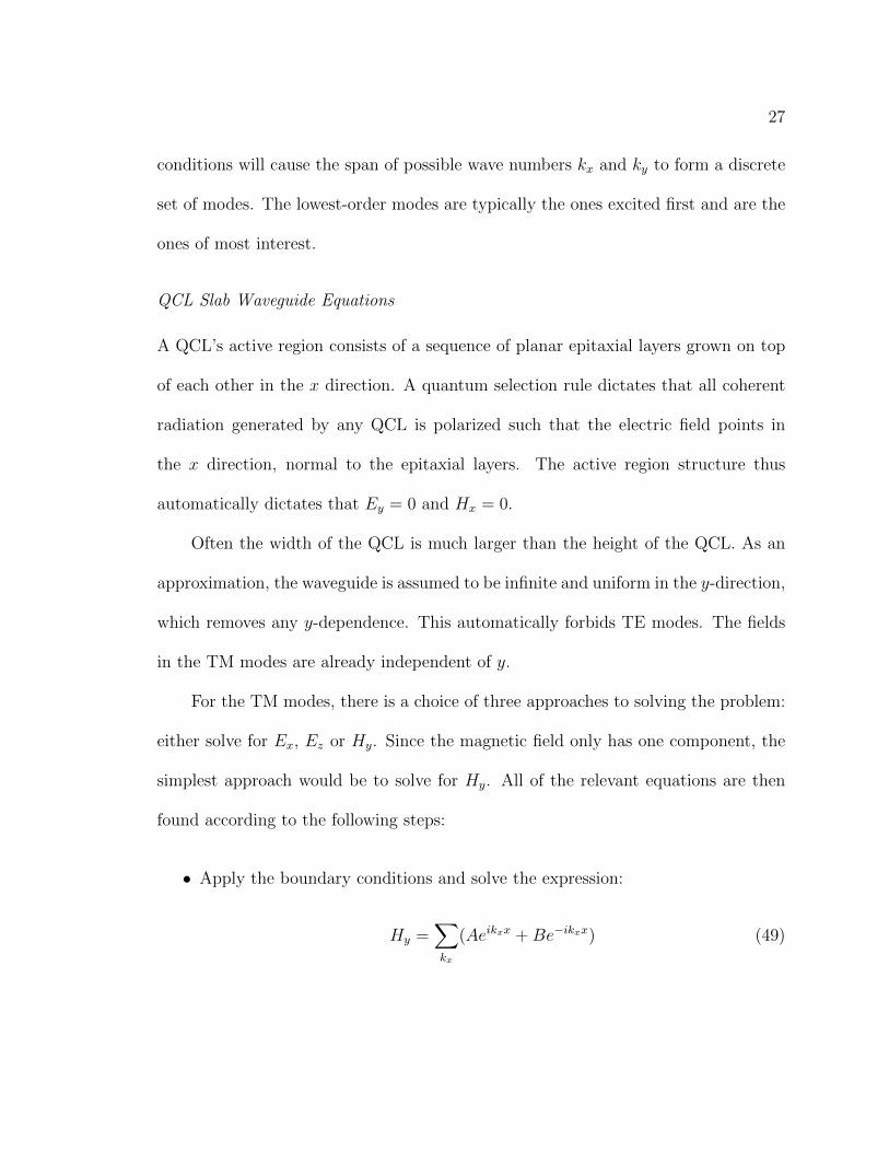
• Apply the boundary conditions and solve the expression:
Hy =∑kx
(Aeikxx +Be−ikxx) (49)
28
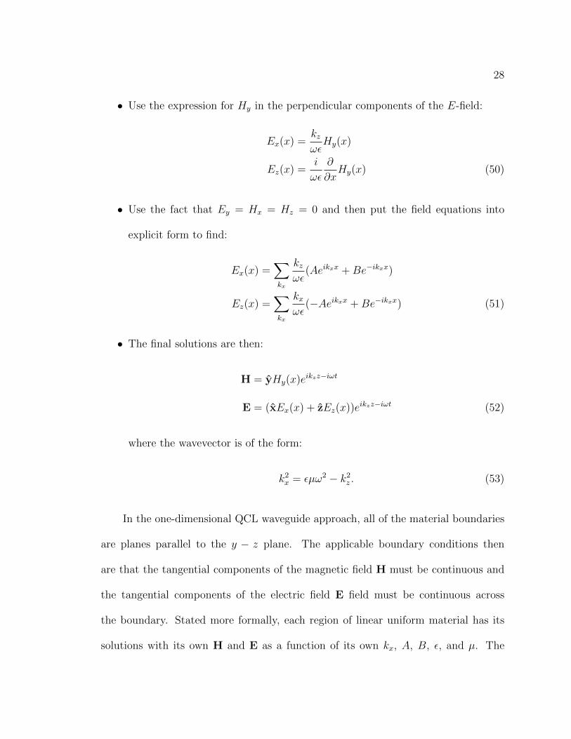
• Use the expression for Hy in the perpendicular components of the E-field:
Ex(x) =kzωεHy(x)
Ez(x) =i
ωε
∂
∂xHy(x) (50)
• Use the fact that Ey = Hx = Hz = 0 and then put the field equations into
explicit form to find:
Ex(x) =∑kx
kzωε
(Aeikxx +Be−ikxx)
Ez(x) =∑kx
kxωε
(−Aeikxx +Be−ikxx) (51)
• The final solutions are then:
H = yHy(x)eikzz−iωt
E = (xEx(x) + zEz(x))eikzz−iωt (52)
where the wavevector is of the form:
k2x = εµω2 − k2z . (53)
In the one-dimensional QCL waveguide approach, all of the material boundaries
are planes parallel to the y − z plane. The applicable boundary conditions then
are that the tangential components of the magnetic field H must be continuous and
the tangential components of the electric field E field must be continuous across
the boundary. Stated more formally, each region of linear uniform material has its
solutions with its own H and E as a function of its own kx, A, B, ε, and µ. The
29
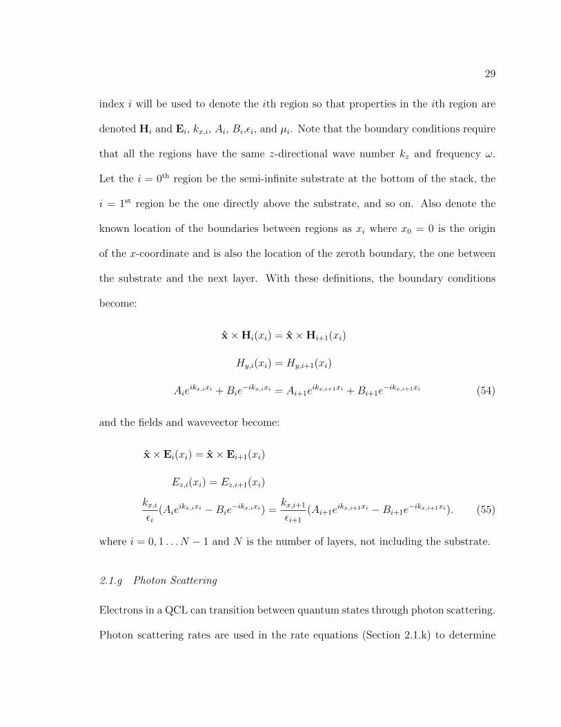
index i will be used to denote the ith region so that properties in the ith region are
denoted Hi and Ei, kx,i, Ai, Bi,εi, and µi. Note that the boundary conditions require
that all the regions have the same z-directional wave number kz and frequency ω.
Let the i = 0th region be the semi-infinite substrate at the bottom of the stack, the
i = 1st region be the one directly above the substrate, and so on. Also denote the
known location of the boundaries between regions as xi where x0 = 0 is the origin
of the x-coordinate and is also the location of the zeroth boundary, the one between
the substrate and the next layer. With these definitions, the boundary conditions
become:
x×Hi(xi) = x×Hi+1(xi)
Hy,i(xi) = Hy,i+1(xi)
Aieikx,ixi +Bie
−ikx,ixi = Ai+1eikx,i+1xi +Bi+1e
−ikx,i+1xi (54)
and the fields and wavevector become:
x× Ei(xi) = x× Ei+1(xi)
Ez,i(xi) = Ez,i+1(xi)
kx,iεi
(Aieikx,ixi −Bie
−ikx,ixi) =kx,i+1
εi+1
(Ai+1eikx,i+1xi −Bi+1e
−ikx,i+1xi). (55)
where i = 0, 1 . . . N − 1 and N is the number of layers, not including the substrate.
2.1.g Photon Scattering
Electrons in a QCL can transition between quantum states through photon scattering.
Photon scattering rates are used in the rate equations (Section 2.1.k) to determine
30
electron and photon populations and, in the end, the laser power (Section 2.1.m).
Photon scattering events include spontaneous photon emission, stimulated photon
emission, and stimulated photon absorption.
The computational model is most complete if there are no assumptions made in
advance as to which transition is the laser transition. This means that the model
calculates the photon scattering rate for all possible transitions. The laser transition
is identified as the one with the most laser power emitted, which is essentially the
one with the highest photon population. The photon population of each transition is
a function of electron population inversion and the photon scattering rate.
General Derivation
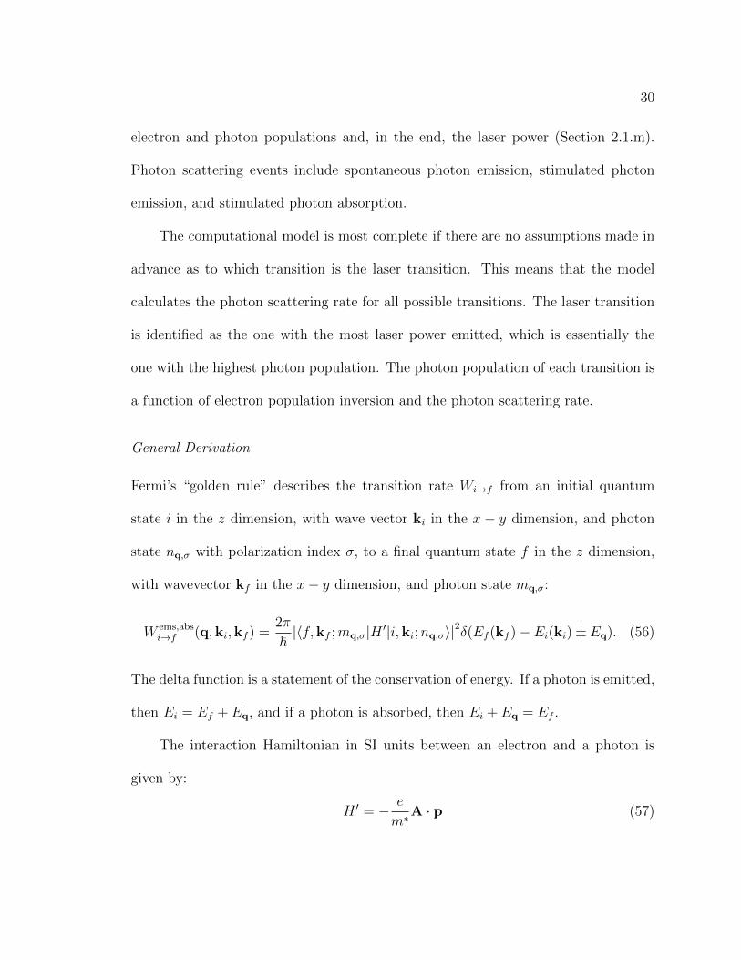
Fermi’s “golden rule” describes the transition rate Wi→f from an initial quantum
state i in the z dimension, with wave vector ki in the x − y dimension, and photon
state nq,σ with polarization index σ, to a final quantum state f in the z dimension,
with wavevector kf in the x− y dimension, and photon state mq,σ:
W ems,absi→f (q,ki,kf ) =
2π
~|〈f,kf ;mq,σ|H ′|i,ki;nq,σ〉|2δ(Ef (kf )− Ei(ki)± Eq). (56)
The delta function is a statement of the conservation of energy. If a photon is emitted,
then Ei = Ef + Eq, and if a photon is absorbed, then Ei + Eq = Ef .
The interaction Hamiltonian in SI units between an electron and a photon is
given by:
H ′ = − e
m∗A · p (57)
31
where A is the electromagnetic vector potential operator describing the photons in-
teracting with the electron, and p is the momentum operator of the electron. The
effective mass is taken from the well material since this is where the electron has the
highest location probability.
In SI units, The Lorentz-Gauge vector potential for a harmonic interaction with
a quantized EM field at a single wave vector q is a sum of creation and annihilation
operators:
A =2∑
σ=1
√~
2εV qc/n
(aq,σεq,σe
iq·r + a†q,σεq,σe−iq·r) (58)
where V is the cavity volume, ε is the dielectric constant, ε is the polarization vector
and q is the wave vector of the photon. Now substitute this expanded Hamiltonian
in Fermi’s “golden rule”:
W ems,absi→f (q,ki,kf ) =
2π
~e2
(m∗)2~
2εV qc/n
(m∗)2(Ef − Ei)2
~2|〈f(z)|z|i(z)〉|2
×
∣∣∣∣∣2∑
σ=1
εσ,z
√nq,σ + 1/2± 1/2
∣∣∣∣∣2
δ(Ef − Ei ± Eq)δkf ,ki. (59)
Summing over all possible final electron momenta and using the Kronecker delta to
ensure conservation of momentum, we find:
W ems,absi→f (q) =
2π
~e2
(m∗)2~
2εV qc/n
(m∗)2(Ef − Ei)2
~2|〈f(z)|z|i(z)〉|2
×
∣∣∣∣∣2∑
σ=1
εσ,z
√nq,σ + 1/2± 1/2
∣∣∣∣∣2
δ(Ef − Ei ± Eq). (60)
By defining some parameters and simplifying the constants, the scattering rate can
also be written as:
W ems,absi→f (q) =
e2hωif4m∗√εrε0V qc
fi→f
∣∣∣∣∣2∑
σ=1
εσ,z
√nq,σ + 1/2± 1/2
∣∣∣∣∣2
δ(Ef − Ei ± Eq) (61)
32
where the oscillator strength is defined as:
fi→f =2m∗ωif
~
∣∣∣∣∫ ψ∗f (z)zψi(z)dz
∣∣∣∣2. (62)
and the resonant frequency is:
ωif =Ei − Ef
~. (63)
The integral matches that found in Smet53 and Harrison54 and is done numerically
using the non-uniform-grid trapezoidal method.
There are two relevant cases that are handled differently: spontaneous photon
emission into all modes, and stimulated photon emission and absorption into a narrow
mode distribution.
Spontaneous Photon Emission into all modes
In this case, Eq. (61) becomes:
W spi→f (q) =
e2hωif4m∗√εrε0V qc
fi→f
∣∣∣∣∣2∑
σ=1
εσ,z
∣∣∣∣∣2
δ(Ef − Ei + Eq). (64)
Summing over all modes in the cavity (assuming an effectively infinite cavity in all
three dimensions) leads to:
W spi→f =
1
(2π/L)3
∫dqW sp
i→f (q)
=1
(2π/L)3
∫dqq2
∫dθ sin θ
∫dφ
e2hωif4m∗√εrε0V qc
fi→f
×
∣∣∣∣∣2∑
σ=1
εσ,z
∣∣∣∣∣2
δ(Ef − Ei + Eq). (65)
33
If the axis is chosen such that ε1 lies in the plane defined by k and q, then ε2,z = 0
and ε1,z = sin θ, which leads to:
W spi→f =
e2nω2if
6πm∗ε0c3fi→f . (66)
This expression is used in the rate equations simply as another scattering mechanism
that effects electron populations. The radiation due to spontaneous emission into
all modes does not contribute to the laser radiation. Note that for typical QCL’s,
the spontaneous photon emission rate into all modes is so small compared to other
scattering mechanisms that it is essentially negligible. However, this calculation is
still included in the computational model because it is easy to implement, runs quickly
and establishes a more complete model.
Stimulated Photon Emission/Absorption into a narrow mode distribution at onepolarization
Starting with the one-mode expression before integrating over all energies, Eq. (61)
becomes:
W sti→f (q) =
e2hωif4m∗√εrε0V qc
fi→fMifδ(Ef − Ei ± Eq). (67)
To mimic reality where the energy levels have finite widths due to their finite lifetimes,
the Dirac delta is replaced with a normalized line shape function in the form of a
Lorentzian (see the appendix of Williams’ thesis52):
W st,bandi→f (q) =
e2ωif4m∗√εrε0V qc
fi→fMifγif (ν) (68)
34
where
γif (ν) =∆νif/2π
(ν − νif )2 + (∆νif/2)2
νif =ωif2π
=Ei − Ef
h(69)
and the full-width half maximum line width of the transition is:
∆νif =1
π
(1
2τi+
1
2τf+
1
T ∗2
). (70)
The parameters τi and τf are the initial and final state total lifetimes and T ∗2 is
the pure dephasing time. The pure dephasing time is a characteristic lifetime that
describes the process of phase randomization that occurs to a collection of oscillators,
as described by Williams.52
The stimulated emission rate must be used in the rate equations in order to
determine the photon populations. The rate equations require a single number for
the transition rate, but the expression above is an entire function. This is solved by
taking the scattering rate at the peak frequency. Setting ν = νif , Eq. (68) becomes:
W st,bandi→f = Mif
e2
2πm∗εV∆νiffi→f (71)
where
fi→f =2m∗ωif
~
∣∣∣∣∫ ψf*(z)zψi(z)dz
∣∣∣∣2∆νif =
1
π
(1
2τi+
1
2τf+
1
T ∗2
). (72)
35
2.1.h Phonon Scattering
Only longitudinal optical (LO) phonon scattering is assumed to be significant in
QCL’s. The phonon spectrum available to a QCL electron for scattering is approx-
imated to be the phonon spectrum of a bulk sample of the material used in the
quantum wells. The assumption is also made that the bulk crystal is dispersionless
such that every LO photon that can be created or destroyed in a transition is at the
frequency ωLO(q) = ωLO(0) regardless of the wavevector q. This is equivalent to a
constant phonon energy of ELO = ~ωLO, which is different for each material, but can
be determined experimentally and found in the literature.
Inside a QCL, the electron is quantized in the z dimension, described by a wave-
function state, and pseudo-free in the x and y dimensions according to the effective
mass model. Scattering between an electron and a phonon is described by the Frohlich
interaction.
General derivation
Fermi’s “golden rule” is written for the transition rate Wi→f from an initial quantized
intersubband state i in the z dimension with wavevector ki in the x − y dimension
and crystal phonon state ni,q to a final intersubband state f in the z dimension with
wavevector kf in the x− y dimension and crystal phonon state nf,q:
W ems,absi→f (ki,kf ) =
2π
~|〈f,kf ;nf,q|H ′|i,ki;ni,q〉|2δ(Ef (kf )− Ei(ki)± ELO). (73)
The delta factor is a statement of the conservation of energy. If a phonon is emitted,
then Ei = Ef + ELO and if a phonon is absorbed, then Ei + ELO = Ef .
36
The interaction Hamiltonian between an electron and a phonon is given by:
H ′ =∑q
[α(q)(eiq·rbq + e−iq·rb†q)
](74)
where b†q and bq are the phonon creation and annihilation operators, respectively.
The interaction strength α(q) is given by the Frohlich representation:
|α(q)|2 =ELO
2
e2
V q2
(1
ε∞− 1
εs
)(75)
where ε∞ and εs are the high and low frequency permittivities, respectively. The
interaction Hamiltonian is a sum of all the possible phonon wavevectors (modes) q.
Although the modes are discreet, the crystal is large enough that the modes are
assumed to be infinitesimally close and the sum is approximated by an integral:
H ′ =L3
(2π)3
∫dqx
∫dqy
∫dqzα(qxi+ qy j + qzk)
×(ei(qxx+qyy+qzz)b(qx i+qy j+qz k) + e−i(qxx+qyy+qzz)b†
(qx i+qy j+qz k)
). (76)
Plugging the Hamiltonian into Fermi’s “golden rule” and moving the integrals
outside of the bra and ket vectors we find:
W ems,absi→f (ki,kf ) =
Le2
~V(nLO + 1/2± 1/2)
ELO
2
(1
ε∞− 1
εs
)×δ(Ef (kf )− Ei(ki)± ELO)
×∫dqz
1
(q2 + q2z)
∣∣〈f(z)|e∓iqzz|i(z)〉∣∣2 . (77)
The transition rate to a quantum state f in the z dimension but any state in the
x− y dimensions is the integral over all possible final states in the x− y dimension:
W ems,absi→f (ki) =
1
(2π/L)2
∫W ems,absi→f (ki,kf )dkf . (78)
37
Applying this sum, and expanding the two-dimensional final wavevector integral into
polar coordinates, the transition rate becomes:
W ems,absi→f (ki) =
1
2
(2m∗
~2
)1
(2π/L)22π
L
(2π)4
L4
L6
(2π)62π
~e2
V(nLO + 1/2± 1/2)
×ELO
2
(1
ε∞− 1
εs
)π
∫ 2π
0
A(q)
qdθ. (79)
The form factor A(q) is the same one that appears in electron-electron scattering
calculations (see Section 2.1.i). To avoid recalculating the same parameters, the form
factors are calculated in advance, before the electron-electron scattering or phonon
scattering calculations. The form factor depends only on the wavefunctions and the
transverse interaction wavenumber q. The model’s runtime is improved significantly
by pre-calculating the form factor outside of the other integrals to form a look-up
table in q. When the phonon scattering integrals are calculated and specific form
factor values are needed for certain q values, they are interpolated from the look-up
table.
After simplifying the constants, the final expression is:
W ems,absi→f (ki) =
m∗e2ELO
8π~3
(1
ε∞− 1
εs
)(nLO + 1/2± 1/2)
∫ 2π
0
A(q)
qdθ (80)
where
A(q) =
∫dz
∫dz′ψi(z)ψf (z)ψf (z
′)ψi(z′)e−q|z−z
′|
q2 = k2i + k2f − 2kikf cos(θ)
k2f = k2i +2m∗
~2(Ei(0)− Ef (0)∓ ELO) . (81)
38
Averaging over all initial wavevectors in Eq. (80) leads to:
Wi,j→f,g =
∫Lx
2πdki,x
∫ Ly
2πdki,yWi,j→f,g(ki)fi(ki)∫
Lx
2πdki,x
∫ Ly
2πdki,yfi(ki)
. (82)
Final Expression
Apply the average of Eq. (82) to get the final expression:
W ems,absi,j→f,g =
m∗e2ELO
8π~3
(1
ε∞− 1
εs
)(nLO + 1/2± 1/2)
∫dkikifi(ki)
∫ 2π
0dθA(q)
q∫dkikifi(ki)
(83)
where
A(q) =
∫dz
∫dz′ψi(z)ψf (z)ψf (z
′)ψi(z′)e−q|z−z
′|
q2 = k2i + k2f − 2kikf cos(θ)
k2f = k2i +2m∗
~2(Ei(0)− Ef (0)∓ ELO) . (84)
The LO phonon energy ELO is taken to be a constant of the material. The phonon
occupation number nLO is taken to be its bulk material value, which is given by
Bose-Einstein statistics to be:
nLO =1
eELO/kT − 1. (85)
These equations match those found in Smet53 and Harrison.54 The integrands are
evaluated computationally as described in Section 2.2.i.
2.1.i Electron-Electron Scattering
Scattering will first be derived without screening. The details of the screening deriva-
tion can be found in Section 2.1.j. Also, the electron-electron exchange interaction will
39
not be discussed here as there are many explanations available in the literature.55–57
The exchange effect was not included in the QCL computational model for this work
but will be included in future versions.
The eigenstate of an electron in the unperturbed Hamiltonian of a QCL (neglect-
ing the Bloch envelope function) is projected into coordinate space:
〈r|ψ〉 = 〈x|ψx〉〈y|ψy〉〈z|ψz〉 =1√Lxeikxx
1√Lyeikyyψn(z) (86)
where Lx and Ly are the lengths of the crystal in the dimension perpendicular to
the growth dimension z and are needed to normalize the effectively free-electron
components of the wave function. The bound-state z-component wavefunctions ψn are
found by numerically solving the one-dimensional Schrodinger equation (Section 2.2.e)
and the Poisson equation (Section 2.2.c) and are understood to be already normalized.
In the most general form, electron-electron scattering in a QCL involves the inter-
action of an electron in an initial quantum state i in the z dimension and wavevector
ki in the x and y dimensions with an electron in state j with wavevector kj so that
they end up, respectively, in states f and g and with wavevectors kf and kg. In the
x and y dimensions, the electron is considered pseudo-free within the effective mass
approximation for bulk semiconductor materials. In these dimensions, the material
is considered to be a bulk volume of the well material.
Variable Definitions
It is worthwhile to anticipate some aspects of the formal derivation and make some
variable definitions in advance. This will simplify the mathematics later on as well
40
as bring the notation in line early on with the literature.
Initially there are four independent, two-dimensional wavevectors: ki, kj, kf
and kg. Because the electrons are pseudo-free in the x-y plane, which is the same
plane in which all these wavevectors lie, the law of conservation of momentum holds
and removes both components of kg as independent variables. In addition, the law of
conservation of energy applies to the whole three-dimensional interaction and removes
kf as an independent variable. The remaining components (ki, θki , kj, θkj and θkf )
are independent and any intermediate variables should be functions of these.
The transition wavevector is defined as q = ki − kf , which leads to:
q =√k2i + k2f − 2kikf cos(θki − θkf ). (87)
The dot product of ki and kj is written as:
k2u = kikj cos(θki − θkj). (88)
This quantity is negative and therefore ku is complex valued. The transition energy
wavenumber g0, which can also be complex, is defined as:
g20 =4m∗
~2[Ei(0) + Ej(0)− Ef (0)− Eg(0)]. (89)
The sum of the initial wavevectors dotted by the unit vector kf is defined as:
ks = ki cos(θki − θkf ) + kj cos(θkj − θkf ). (90)
The initial relative wavevector is defined as g = kj − ki (it is also referred to as kij).
41
Written in terms of magnitude and phase, this wavevector is expressed as:
g =√k2j + k2i − 2k2u
tan θg =kj sin θkj − ki sin θkikj cos θkj − ki cos θki
. (91)
Similarly, the final relative wavevector is defined as g′ = kg − kf (it is also referred
to as kfg). Written in terms of magnitude and phase, the wavevector becomes:
g′ =√k2g + k2f − 2kgkf cos(θkg − θkf )
tan θg′ =kg sin θkg − kf sin θkfkg cos θkg − kf cos θkf
. (92)
Finally, the relative angle θ between the initial and final relative wavevectors is defined
as θ = θg − θg′ . All of the above definitions lead to the energy difference relation:
g2 − g′2 = k2i + k2j − k2f − k2g − 2k2u + 2kfkg cos(θkf − θkg). (93)
Conservation of energy (Ei + Ej = Ef + Eg) is now applied and used to fur-
ther simplify the variables defined above. Expanding the energy into x, y, and z
components yields:
Ei(0) +~2k2i2m∗
+ Ej(0) +~2k2j2m∗
= Ef (0) +~2k2f2m∗
+ Eg(0) +~2k2g2m∗
(94)
and using the energy wavenumber from Eq. (89), the energy conservation condition
reduces to:
1
2g20 + k2i + k2j = k2f + k2g . (95)
The dependence on kg is removed using the conservation of momentum to obtain:
g20 − 4k2f − 4k2u + 4kfks = 0. (96)
42
There are two ways to solve Eq. (96): using kf directly or using g′, which depends on
kf . Both methods are shown and implemented below as a check that no errors have
been made.
Solving Eq. (96) for kf leads to:
kf =1
2ks ±
1
2
√k2s + g20 − 4k2u. (97)
Note that there are two possible solutions in this equation and sometimes both are
valid, so each possibility must be calculated and summed together.
Alternatively, a solution to Eq. (96) can be found for g′. This is done by first
transforming all variables into g and g′. The last three terms in Eq. (96) are equal to
(g2 − g′2):
g20 + g2 − g′2 = 0. (98)
This leads to the intuitive statement that the transition energy equals the energy
difference. Solving for g′ leads to the result:
g′ =√g20 + g2. (99)
General Derivation of the Scattering Rate for one ki
Now that the preliminary definitions have been made a formal derivation can now be
done. The conservation laws will appear automatically and will be applied as they
appear. All of the variable definitions and relations found in the previous section will
be used directly here without much need of further comment.
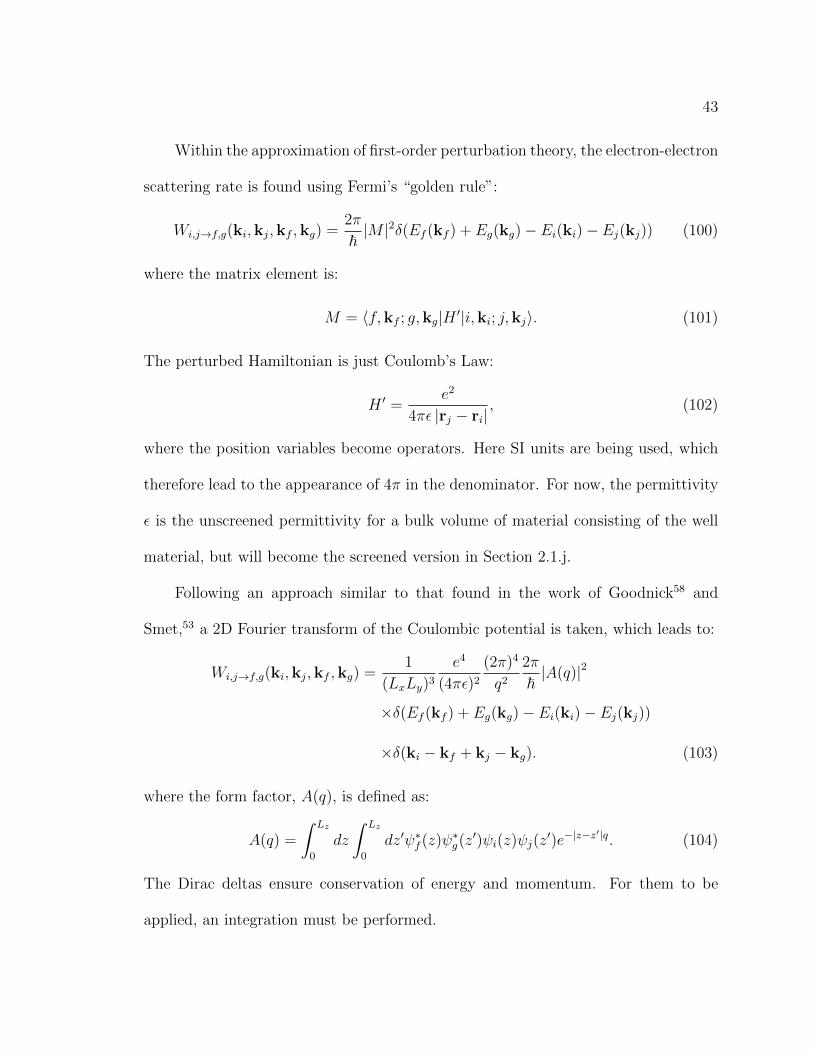
43
Within the approximation of first-order perturbation theory, the electron-electron
scattering rate is found using Fermi’s “golden rule”:
Wi,j→f,g(ki,kj,kf ,kg) =2π
~|M |2δ(Ef (kf ) + Eg(kg)− Ei(ki)− Ej(kj)) (100)
where the matrix element is:
M = 〈f,kf ; g,kg|H ′|i,ki; j,kj〉. (101)
The perturbed Hamiltonian is just Coulomb’s Law:
H ′ =e2
4πε |rj − ri|, (102)
where the position variables become operators. Here SI units are being used, which
therefore lead to the appearance of 4π in the denominator. For now, the permittivity
ε is the unscreened permittivity for a bulk volume of material consisting of the well
material, but will become the screened version in Section 2.1.j.
Following an approach similar to that found in the work of Goodnick58 and
Smet,53 a 2D Fourier transform of the Coulombic potential is taken, which leads to:
Wi,j→f,g(ki,kj,kf ,kg) =1
(LxLy)3e4
(4πε)2(2π)4
q22π
~|A(q)|2
×δ(Ef (kf ) + Eg(kg)− Ei(ki)− Ej(kj))
×δ(ki − kf + kj − kg). (103)
where the form factor, A(q), is defined as:
A(q) =
∫ Lz
0
dz
∫ Lz
0
dz′ψ∗f (z)ψ∗g(z′)ψi(z)ψj(z
′)e−|z−z′|q. (104)
The Dirac deltas ensure conservation of energy and momentum. For them to be
applied, an integration must be performed.
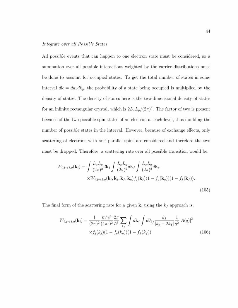
44
Integrate over all Possible States
All possible events that can happen to one electron state must be considered, so a
summation over all possible interactions weighted by the carrier distributions must
be done to account for occupied states. To get the total number of states in some
interval dk = dkxdky, the probability of a state being occupied is multiplied by the
density of states. The density of states here is the two-dimensional density of states
for an infinite rectangular crystal, which is 2LxLy/(2π)2. The factor of two is present
because of the two possible spin states of an electron at each level, thus doubling the
number of possible states in the interval. However, because of exchange effects, only
scattering of electrons with anti-parallel spins are considered and therefore the two
must be dropped. Therefore, a scattering rate over all possible transition would be:
Wi,j→f,g(ki) =
∫LxLy(2π)2
dkj
∫LxLy(2π)2
dkf
∫LxLy(2π)2
dkg
×Wi,j→f,g(ki,kj,kf ,kg)fj(kj)(1− fg(kg))(1− ff (kf )).
(105)
The final form of the scattering rate for a given ki using the kf approach is:
Wi,j→f,g(ki) =1
(2π)2m∗e4
(4πε)22π
~3∑kf
∫dkj
∫dθkf
kf|ks − 2kf |
1
q2|A(q)|2
×fj(kj)(1− fg(kg))(1− ff (kf )) (106)
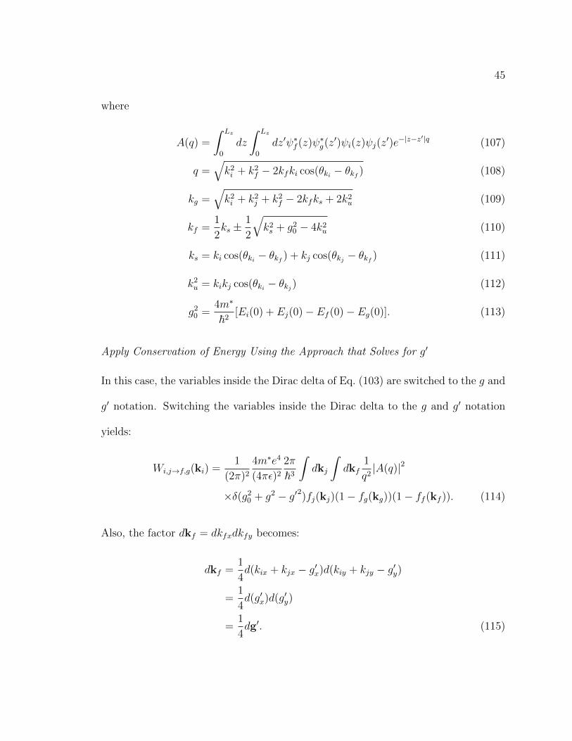
45
where
A(q) =
∫ Lz
0
dz
∫ Lz
0
dz′ψ∗f (z)ψ∗g(z′)ψi(z)ψj(z
′)e−|z−z′|q (107)
q =√k2i + k2f − 2kfki cos(θki − θkf ) (108)
kg =√k2i + k2j + k2f − 2kfks + 2k2u (109)
kf =1
2ks ±
1
2
√k2s + g20 − 4k2u (110)
ks = ki cos(θki − θkf ) + kj cos(θkj − θkf ) (111)
k2u = kikj cos(θki − θkj) (112)
g20 =4m∗
~2[Ei(0) + Ej(0)− Ef (0)− Eg(0)]. (113)
Apply Conservation of Energy Using the Approach that Solves for g′
In this case, the variables inside the Dirac delta of Eq. (103) are switched to the g and
g′ notation. Switching the variables inside the Dirac delta to the g and g′ notation
yields:
Wi,j→f,g(ki) =1
(2π)24m∗e4
(4πε)22π
~3
∫dkj
∫dkf
1
q2|A(q)|2
×δ(g20 + g2 − g′2)fj(kj)(1− fg(kg))(1− ff (kf )). (114)
Also, the factor dkf = dkfxdkfy becomes:
dkf =1
4d(kix + kjx − g′x)d(kiy + kjy − g′y)
=1
4d(g′x)d(g′y)
=1
4dg′. (115)
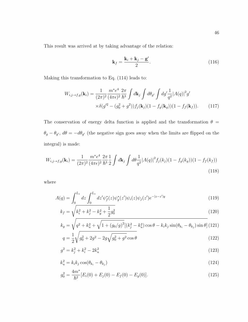
46
This result was arrived at by taking advantage of the relation:
kf =ki + kj − g′
2. (116)
Making this transformation to Eq. (114) leads to:
Wi,j→f,g(ki) =1
(2π)2m∗e4
(4πε)22π
~3
∫dkj
∫dθg′
∫dg′
1
q2|A(q)|2g′
×δ(g′2 − (g20 + g2))fj(kj)(1− fg(kg))(1− ff (kf )). (117)
The conservation of energy delta function is applied and the transformation θ =
θg − θg′ , dθ = −dθg′ (the negative sign goes away when the limits are flipped on the
integral) is made:
Wi,j→f,g(ki) =1
(2π)2m∗e4
(4πε)22π
~31
2
∫dkj
∫dθ
1
q2|A(q)|2fj(kj)(1− fg(kg))(1− ff (kf ))
(118)
where
A(q) =
∫ Lz
0
dz
∫ Lz
0
dz′ψ∗f (z)ψ∗g(z′)ψi(z)ψj(z
′)e−|z−z′|q (119)
kf =
√k2i + k2j − k2g +
1
2g20 (120)
kg =
√q2 + k2u +
√1 + (g0/g)2[(k2j − k2u) cos θ − kikj sin(θki − θkj) sin θ] (121)
q =1
2
√g20 + 2g2 − 2g
√g20 + g2 cos θ (122)
g2 = k2j + k2i − 2k2u (123)
k2u = kikj cos(θki − θkj) (124)
g20 =4m∗
~2[Ei(0) + Ej(0)− Ef (0)− Eg(0)]. (125)
47
This form agrees with that of Goodnick58 and Smet53 when errors in these works are
corrected according to Moskova’s suggestions.55
Scattering Rate Averaged Over ki
The actual wavevector ki of the specific electron of interest is not known, so it must
be averaged over a typical distribution of ki to get an average scattering rate. This is
done by summing up all the scattering rates for all the different states and dividing
by the number of states. As before, the density of occupied states in an interval dki
is the density of states at this value times the probability of occupation, which is the
Fermi function:
Wi,j→f,g =
∫ LxLy
(2π)2dkiWi,j→f,g(ki)fi(ki)∫ LxLy
(2π)2dkifi(ki)
. (126)
Canceling terms and expanding the integral into polar coordinates leads to:
Wi,j→f,g =
∫dk i∫kidθkiWi,j→f,g(ki)fi(ki)∫dk i∫kidθkifi(ki)
. (127)
2.1.j Electron-Electron Screening
The scattering of one electron with one other electron has already been derived in
Section 2.1.i. While screening involves a multi-electron interaction, the multi-electron
Hamiltonian is too complicated to be solved and is therefore approximated. If it is
assumed that two electrons scatter in the absence of any other charged particles, then
the previous treatment still applies. If it is assumed that all the other electrons are
not negligible, but are far enough way that they behave semi-classically as a sea of
electrons that exert a net influence, then screening must be taken into account.
48
The presence of other electrons tends to weaken the interaction between two elec-
trons and therefore the effect is described as screening. Classically, this macroscopic
screening effect in matter is handled by replacing the permittivity of free space with
a permittivity value that is representative of the material. Some level of screening
was already incorporated in Section 2.1.i since the material’s permittivity was used.
However, that permittivity is for a bulk volume of material. In QCL’s, nano-scale
layers of differing materials lead to quantum wells and quantized states for the elec-
trons which do the screening. In order to incorporate a more exact form of screening,
the bulk permittivity should be replaced with a new permittivity that depends on the
quantized states. Once the screened permittivity has been found, it is incorporated
into the innermost integrand of the e-e scattering equation from Eq. (118).
A general expression for the permittivity of a solid is derived using a self-
consistent field (SCF) approach, which has been shown to be equivalent to a random-
phase approximation (RPA) approach by Haug.59
General Screening Expression
By definition, the relative permittivity connects the polarization field P with the total
electric field E inside a material as described by the relation:
P = ε0(εr − 1)E. (128)
Causality dictates that induced polarization fields at different times and places
add together to a total field at a certain time and place. This means that the solution
would be an integral over many time points. Instead, a transformation to frequency
49
space is made, which reduces the polarization dependency to just one wave number
component q:
P(q, t) = εs(εr(ω,q)− 1)E(q, t). (129)
Here, εs is the static permittivity of the material and εr is a relative permittivity
screening constant that represents how the total permittivity deviates from the static
value. Solving for the screening constant leads to:
εr(ω,q) = 1 +P(q, t)
εsE(q, t). (130)
The electric field is expressed in terms of the negative gradient of a total potential V .
Doing this and performing a Fourier transform yields:
E(x, t) = −∇V (x, t)
E(q, t) = −iqV (q, t). (131)
The polarization field is created by the induced charge density ρpol. Using this and
performing a Fourier transform leads to:
∇ ·P(x, t) = −ρpol(x, t)
iq ·P(q, t) = −ρpol(q, t). (132)
Plugging both the electric and polarization field into the permittivity relation of
Eq. (130) yields:
εr(ω,q) = 1− P(q, t)
εsiqV (q, t)
εr(ω,q) = 1 +iq ·P(q, t)
εsq2V (q, t)
εr(ω,q) = 1− 1
εsq2ρpol(q, t)
V (q, t). (133)
50
The classical induced charge density is the sum over the different energy states of the
quantum density matrix:
ρpol(q, t) = − e
L3
∑k
〈k|ρ1|k + q〉. (134)
In order to get the ratio of the density matrix to the potential in terms of quantum
statistical distributions, the Louisville equation and first-order perturbation theory is
applied, which yields:
ρpol(q, t)
V (q, t)=〈k|ρ1|k + q〉V (q, t)
= ef(Ek+q)− f(Ek)
Ek+q − Ek − ~ω. (135)
This ratio is plugged back into Eq. (133):
εr(ω,q) = 1 +e2
εsq2L3
∑k
f(Ek+q)− f(Ek)
Ek+q − Ek − ~ω. (136)
This is the general expression for the relative permittivity in terms of quantum distri-
butions, in SI units. For a two-dimensional system with a quantized third dimension,
and in the static limit, this becomes:
εr(q) = 1 +e2
εsqL2Aiiii(q)
∑k
fi(Ei,k+q)− fi(Ei,k)
Ei,k+q − Ei,k(137)
where Aiiii(q) is the intrasubband form factor for the initial electron state. A polar-
izability function is defined as:
Πii(q) =2
L2
∑k
fi(Ei,k+q)− fi(Ei,k)
Ei,k+q − Ei,k(138)
and the permittivity is rewritten as:
εr(q) = 1 +e2
2εsqΠii(q)Aiiii(q). (139)
51
In reality, an electron is screened by all the electrons in all subbands, not just its own.
Therefore, a sum over all subbands is performed:
εr(q) = 1 +e2
2εsq
∑i
Πii(q)Aiiii(q). (140)
Expanding out the Fermi distributions and energies of Eq. (138), the polarizabil-
ity becomes:
Πii(q) =2
L2
∑k
[1 + exp
(~2|ki+q|2
2m∗ −EF,i
kBT ie
)]−1−[1 + exp
(~2k2i2m∗ −EF,i
kBT ie
)]−1~2|ki+q|2
2m∗− ~2k2i
2m∗
. (141)
Polarizability at Zero Temperature
For the special case of zero temperature, T = 0, this reduces to:
Πii(q, kF,i, T = 0) =m∗
~2π
[1− θ(q − 2kF,i)
√1− (2kF,i/q)2
]. (142)
This polarization function contains the Fermi wavevector, which is defined as:
kF,i =√
2m∗EF,i/~. (143)
This also assumed that the crystal is large enough that the set of quantum states for
the electron becomes a continuous band of states.
Polarizability at Any Temperature
To solve for any temperature, the Fermi functions must be expressed differently.
Starting with the definition of the hyperbolic tangent:
tanhx =ex − e−x
ex + e−x(144)
52
and expanding tanh into its integral form leads to the relationship:
1
1 + ex=
1
2
∫ ∞x/2
dx′
cosh2 x′. (145)
The integral can span all positive numbers if the lower contribution is forced to be
zero using the Heaviside step function (θ(x) = 1 if x > 0, θ(x) = 0 if x < 0):
1
1 + ex=
1
2
∫ ∞0
θ(x′ − x/2)dx′
cosh2 x′. (146)
Using this identity, the general polarizability expression becomes:
Πii(q) =4
(2π)2
∫ ∞0
dk′k′
4kBT ie cosh2(
~2(k′2−k2F,i)
4m∗kBT ie
) [∫ ∞0
dk
∫ 2π
0
kdθ
(1
q2 + 2kq cos(θ)
)× (θ
(k′2 − k2 − q2 − 2kq cos θ
)− θ
(k′2 − k2
))]. (147)
Comparing the factor in brackets to the T = 0 expression, it is seen that they match
except that this factor is a function of the integration variable k′:
Πii(q) =~2
m∗
∫ ∞0
dk′k′Πii(q, k
′, T = 0)
4kBT ie cosh2(
~2(k′2−k2F,i)
4m∗kBT ie
) . (148)
Final Form of Screening
In summary, there is one screening constant used for all subbands and it is found
using the expression:
εr(q) = 1 +∑i
e2
2εsqΠii(q)Aiiii(q) (149)
53
where
Πii(q) =
∫ ∞0
dEΠii(q, E, T = 0)
4kBT ie cosh2(E−EF,i
2kBT ie
)Πii(q, k
′, T = 0) =m∗
~2π
[1− θ(q − 2k′)
√1− 4k′2/q2
]E =
~2k′2
2m∗. (150)
This polarization function has the added benefit of accommodating individual sub-
band temperatures, which allows the results of the electron temperature model (see
Section 2.1.l) to be used. The integral is computed numerically, as described in Sec-
tion 2.2.k.
Comparison with Literature
This derivation is consistent with the general one put forth by Maldague60 and Ando.61
Harrison also derives a form of e-e screening,54 but makes the assumption that
E = EF in the zero-temperature polarizability. He therefore takes the polarizability
out of the integral, so that the integral is evaluated analytically. Harrison finds the
polarizability to be:
Πii(q) =m∗
2~2π(1 + tanh(EF/2kBT ))
[1− θ(q − 2kf )
√1− 4k2f/q
2]
(151)
This form was found to lead to significant errors by our team.
2.1.k Rate Equations
Once all of the scattering rates are known, the rate equations are applied to determine
the level populations as described by Donovan.62 Use of the rate equations assumes
54
that the system is in a state of equilibrium. This means that the total rate at which
electrons transition into a given level is equal to the total rate at which electrons
transition out. The total rate is the the transition rate of one electron times the
number of electrons in the initial state. The rate equations therefore form a series of
coupled equations. In this model, the photon populations are solved self-consistently
with the electron populations. There is a photon population associated with each
possible transition, and a rate equation for each photon population. In order to
attain completeness and accuracy, all possible electron and photon populations in the
three period structure are included in the rate equations.
Definitions and Notation
There are N quantum states in the three repetitions of the QCL core period, spanning
from i = 0 to i = N − 1. The computational model finds the electron population
ni of each level as well as the photon population mij of each possible transition.
At this point in the calculations, the model has already found all transition rates
Wij from level i to level j: electron-photon scattering, electron-electron scattering,
and electron-phonon scattering (see Sections 2.1.g, 2.1.h and 2.1.i). Also known is
the total electron density ntot which is the sum of all the level populations in one
period and remains constant. The model has already found the waveguide loss αw,
the mirror loss αm, the confinement factor Γ, and the photon cavity loss rate W pij at
many frequencies (see Section 2.1.f).
The current cannot be known since it depends on the populations. Therefore,
55
electrons flowing into and out of one period of the QCL must be accounted for by
assuming the structure is periodic and at equilibrium so that all the electrons flowing
out of the period must flow back into the period. The middle of the three numerically
calculated QCL periods is taken to be the most accurate and is the one used. This
raises the dilemma of how to handle wavefunctions and transitions that span several
periods.
One way to accomplish this is to find the center of mass of each wavefunction
and treat the wavefunction as located in the period containing its center of mass. For
the purpose of enforcing periodicity, transitions are considered to happen between
the center-of-mass points of each state. Based on the center-of-mass approach, this
reduces the periodicity problem to four cases:
1. A transition starting in the central period and ending in the central period.
2. A transition starting in the central period and ending in the outer periods and
vice versa. This must be handled by matching up corresponding wavefunctions
in different periods and tying them to the same population variable.
3. A transition starting in one outer period and ending in the other outer pe-
riod. These are two-period transitions and are again handled by matching up
equivalent wavefunctions.
4. A transition starting and ending in the same outer period. These are ignored
as they are redundant to the first case.
56
Derivations
At equilibrium, the sum of all possible transition rates into the level and out of the
level are equal. The sum is done over every type of transition (electron-electron,
electron-phonon, electron-photon) and over every possible combination of initial and
final level in all three periods:
0 =N−1∑j 6=i
Wjinj − niN−1∑j 6=i
Wij +N−1∑j 6=i
W st,1modeji nj − ni
N−1∑j 6=i
W st,1modeij . (152)
The first term in Eq. (152) is the sum over all non-stimulated photon emission
transitions coming into level i. The second term is the sum over all non-stimulated
photon emission transitions leaving level i. The third term is all of the stimulated pho-
ton emission transitions coming into level i. The fourth term is all of the stimulated
photon emission transitions leaving level i.
The stimulated absorption and emission rates are equal, W st,1modeji = W st,1mode
ij ,
leading to:
0 =N−1∑j 6=i
Wjinj − niN−1∑j 6=i
Wij −N−1∑j=0
W st,1modeij (ni − nj) . (153)
The total stimulated emission rate is just the one-mode spontaneous rate times the
total number of photons Mij available to stimulate:
W st,1modeij = MijW
sp,1modeij . (154)
There is a photon numberMij corresponding to every possible transition and each
photon population also has a rate equation to be solved. Because both the stimulated
absorption rate and stimulated emission rate are equal, they are both dependent
57
on the one-mode spontaneous emission rate. This is handled in the computational
model by making the one-mode spontaneous emission matrix symmetric so that Wij =
Wji. Even though spontaneous emission cannot happen for transitions which increase
energy, this is still valid because the one-mode spontaneous emission rates are only
used to determine the stimulated rates, which can both increase and decrease in
energy.
The number of photons in a certain mode in the cavity that are available to
stimulate emission are set equal to the one-mode photon population density mij
times the volume V of the active region:
Mij = mijV. (155)
Inserting this into the Eq. (153) yields:
0 =N−1∑j 6=i
Wjinj − niN−1∑j 6=i
Wij −N−1∑j=0
mijVWsp,1modeij (ni − nj) . (156)
This expression represents a set of N coupled equations. This is solved numerically
by using fixed point iteration (i.e. solve for ni in terms of nj in order to establish iter-
ation equations). Start with an estimated set of populations and apply the iteration
equation repeatedly, treating ni as the next iterated value of the population densities
and nj as the current value:
ni =
∑N−1j 6=i nj
[Wji +mijVW
sp,1modeij
]∑N−1
j 6=i
[Wij +mijVW
sp,1modeij
] . (157)
This equation is repeated iteratively, setting nj = ni after each step, until the
population densities converge to a value. After each iteration, the populations must be
58
normalized so that their sum equals the total average electron density. One of the rate
equations is redundant and the populations are under-specified by the rate equations.
Applying the normalization is required to find a unique solution. The coupled rate
equations could also be solved using matrix inversion techniques. However, fixed-
point iteration was found to be easier to implement, and not significantly slower or
less accurate then matrix techniques.
Periodic boundary conditions, which take into account the total current entering
and leaving a period, are implemented by treating each level of the three period
numerical array of data as independent. Therefore, the rate equations are solved as
if they are independent, and, at the end of each iteration, the population densities
are copied from the levels in the central period to the equivalent levels in the outer
periods. This requires knowing which wavefunctions are equivalent to each other.
Each photon population present also has a rate equation at equilibrium:
0 = VW st,1modeij ni − VW st,1mode
ji nj + VW sp,1modeij ni − VpmijW
pij. (158)
The first term is the total rate at which photons are added to the cavity in mode
ij due to stimulated emission. The second term is the total rate at which photons
are removed from the cavity in mode ij due to stimulated absorption. The third
term is the total rate at which photons are added to the cavity in mode ij due to
spontaneous emission. The fourth term is the rate at which photons are removed due
to the waveguide losses and mirror losses, where W pij is the total photon cavity loss
rate at the frequency corresponding to the ij transition.
59
The photon loss rate is a function of the waveguide loss, mirror loss and group
velocity according to W pij = (αw + αm)vg. These values are pre-calculated in the
waveguide model as a frequency-dependent look-up table (see Section 2.2.g). In these
rate equation calculations, the frequency of the transition is used to look up the pho-
ton cavity loss rate for that photon population. The electrons able to be stimulated
are only in the active region, so that the active region volume V must be multiplied
by the electron population densities to get the total number. However, all photons
can be lost (those in the active region and in the outer waveguide layers) so that the
cavity volume Vp must be used to find the total number of photons lost.
Dividing every term by Vp and recognizing the known confinement factor Γ =
V/Vp:
0 = ΓW st,1modeij ni − ΓW st,1mode
ji nj + ΓW sp,1modeij ni −mijW
pij. (159)
This equation exists for every possible pair of initial electron level i and final electron
level j. The density of photons mij with a frequency and polarization corresponding
to the ij transition is assumed to be in equilibrium.
A photon population corresponds to a pair of levels involved in the transition and
includes both i to j and j to i transitions. In order to avoid redundant calculations,
this equation is only implemented when the initial level is higher in energy than the
final level. The opposite calculation (lower to higher) should not be done because it
gives redundant information (because mij = mji) and requires a different equation.
The computational model simply calculates only down transitions when finding the
photon populations, then copies the populations to the up transition slots for use in
60
future calculations.
Again using W st,1modeij = mijVW
sp,1modeij and W st,1mode
ji = W st,1modeij where V is
the active region volume leads to:
0 = ΓmijVWsp,1modeij (ni − nj) + ΓW sp,1mode
ij ni −mijWpij. (160)
Solving for the photon populations yields:
mij =ni
W pij/(ΓW
sp,1modeij )− V (ni − nj)
. (161)
2.1.l Electron Temperature
All electrons on average can acquire a temperature (Te) different from the lattice
temperature (TL) due to the applied bias and exchanged energy between the elec-
tron subbands and the lattice as described by Troccoli.63 Additionally, each electron
subband can have a different temperature. These differences are vital to the inter-
nal physics of QCL’s since the subband energy distributions are dependent on the
subband temperature. Therefore, the scattering rates, population densities and all
subsequent calculations are also affected by electron temperature. The harmful ef-
fects of temperature on device performance have been studied extensively by Indjin,
Jirauschek and Lever.64–66
The electron temperatures for each subband can be found through a MC proce-
dure, but not from a simple self-consistent model. When self-consistent models are
modified to account for electron heating, typically only an average Te for the entire
conduction band is found as seen in several papers.67–70 However, Monte Carlo (MC)
61
simulations in the literature39,44,71–76 and experimental measurements by Vitiello77,78
have shown that there is considerable variation among subband temperatures, espe-
cially in resonant phonon QCL designs. In order to determine a separate Te for every
subband using the self-consistent model, a multi-subband energy balance condition
must be implemented as proposed by Ikonic and Jovanovic.42,79
A self-consistent energy balance (SCEB) condition which determines the tem-
perature for electron conduction subbands is described below. This additional com-
ponent to the computational model permits the determination of individual electron
subband temperatures. The effects of electron subband heating on carrier transport
within QCL’s can then be assessed. The specific implementation in the model as well
as the associated algorithm is described in Section 2.2.m.
Subband electron temperature
If a lasing QCL is assumed to reach a steady-state condition, as was the case when
considering the electron population densities, then the rate of change of energy for
a subband is assumed to be constant. Therefore, the subband electron temperatures
(T ie) can be determined by a set of energy balance equations as described by Jo-
vanovic.42 This is similar to the average electron temperature equation put forth by
Harrison.67 In the energy balance equations, the potential energy is defined as the
subband energy minimum (or the quantized eigenenergy). The kinetic energy, which
is related to the electron temperature, is defined as any additional energy above that
minimum. Although the average electron temperature equation can be solved using
62
just the electron eigenenergies, a multi-subband equation also requires the electrons’
kinetic energy. An average subband kinetic energy is found by taking advantage of
the fact that in a QCL, electrons are quasi-free in two-dimensions. This permits the
use of the classical result that the average kinetic energy per degree of freedom is
12kBT . Therefore, the average electron kinetic energy in a subband i is:
βi = kBTie (162)
where kB is Boltzmann’s constant.
The multi-subband energy balance condition is met when the rate of energy
lost from transitions out of each subband is equal to the rate of energy gained from
transitions into each subband. For a single particle transition between two states,
i→ f , the rate of change of energy out of subband i is the average kinetic energy of
an electron in subband i (measured from the minimum of subband i) multiplied by
Wif . This energy rate is also multiplied by the population density of the initial state ni
within the balance equations to properly weight each subband energy rate. However
the same single particle transition also affects subband f . From the perspective of
subband f , the rate of change of energy of subband f is the average kinetic energy of
an electron coming into subband f multiplied by Wif . The average kinetic energy of
this particle must be determined using conservation of energy by taking into account
the energy Ei as well as any additional scattering particles (such as phonons), which
also contribute to the energy transition. In general, the energy balance condition for
63
a subband f is:
dEfdt
=∑i
ni〈Ekf 〉Wif − nf
∑i
βfWfi (163)
where 〈Ekf 〉 is the average kinetic energy in subband f as determined using conser-
vation of energy. For transitions involving one electron, the average kinetic energies
are related according to:
〈Ekf 〉 = Ei + βi − Ef + δE (164)
where δE represents the energy of the scattering particle. The single particle scatter-
ing mechanisms included in the computational model were:
δE =
ELO for phonon absorption
−ELO for phonon emission.
(165)
The balance condition for e-e transitions is more complex since not only does it
involve four particle states, but it also has to be determined from a four-dimensional
matrix of scattering events. In this case, the energy transition rate is:
dEe-ef
dt=∑ijg
ni〈Ekf 〉W e-e
ijfg − nf∑gij
βfWe-efgij (166)
where W e-eijfg is the rate for two electrons in the initial states i and j that scatter to
the states f and g, respectively, and:
〈Ekf 〉 = Ei + βi + Ej + βj − Ef − Eg − βg. (167)
Finally, all forms of scattering which contribute to the rate of change of energy
into and out of a subband f must meet the energy balance condition:
dEemf
dt+dEabs
f
dt+dEe-e
f
dt= 0. (168)
64
Since the scattering rates, population densities and kinetic energies in Eq. (168) are
temperature dependent, the temperature of each subband has to be varied until the
balance condition is met for all subbands. This is accomplished using an iterative
procedure with the entire multi-subband SCEB model, as described in Section 2.2.m).
Average electron temperature
Due to it’s simplicity and successful application in mid-infrared QCL’s (see works by
Harrison67 and Spagnolo80), an average electron temperature is often calculated for
the entire device. This has the advantage of considerably reducing the computation
time for an iteration of the computational model; however, potentially valuable in-
formation is lost since there may be considerable variation among subband electron
temperatures. Additionally, Terazzi has suggested that using a single temperature
to describe electron heating can lead to overly pessimistic predictions of laser perfor-
mance.81
The average electron temperature energy balance condition is found by simply
summing the subband energy balance condition of Eq. (168) over all subbands. It is
often rewritten as:
∆ =∑
em,abs,e−e
∑f
∑i
niτif
(Ei − Ef − δE) = 0 (169)
where δE is equal to −ELO for phonon emission (em), +ELO for phonon absorption
(abs), and zero for electron-electron (e-e) scattering.
It should be noted that electron-photon scattering does not have to be considered
in either Eqs. (168) or (169) since the absorption or emission of a photon by an electron
65
negligibly changes its kinetic energy due to conservation of momentum. However, the
indirect effects of photon scattering on energy balance through electron population
alterations are automatically included.
2.1.m Output Power
Finding the laser output power at a certain frequency is the end purpose of the QCL
computational model. The photon population at a certain frequency is found self-
consistently using the rate equations (see Section 2.1.k). With the photon population
known, it is straight-forward to find the output power from the population and the
device characteristics. In theory, the output power only needs to be calculated from
the population at the end of the calculations, after all self-consistent loops have
converged. In practice, it is helpful to the user to have an order-of-magnitude estimate
of the optical power before the loops converge. For this reason, the output power
calculations are placed inside the loops and calculated every time a new photon
population is found. Considering the fact that the output power calculations are
very simple and quick to perform, placing them inside the loops does not incur any
substantial run-time degradation.
The QCL computational model does not ask the user to specify in advance which
transition is the laser transition. Rather, it is the task of the model to determine
the laser transition. In order to do this, the rate equations calculate the photon
populations for all possible transitions. Further, the output powers are calculated for
all possible transitions. The laser transition is then identified as the one with the
66
highest output power.
Large photon populations are likely for transitions with frequencies below 1 THz
in addition to the frequency of interest. However, such laser frequencies do not
occur experimentally. The reason for this is that traditional QCL waveguides do not
support modes at frequencies below 1 THz, as the loss is too high and the confinement
too low. It is therefore imperative for the QCL computational model to properly
calculate the waveguide effects at low frequencies and apply them as part of the photon
population and output power calculations in order to realistically damp down the high
power response of low frequency transitions. Slight inaccuracies in the waveguide
calculations can lead to false predictions of high-power, low-frequency lasing.
Derivation
The laser radiated output power Pout at a certain frequency is the energy emitted per
unit time out of the front facet. The radiated power at a frequency equals the total
number of photons M at that frequency emitted per unit time, times the energy per
photon E:
Pout(ω) = ME = M~ω. (170)
The number of photons of a certain frequency being emitted per unit time out
the front surface of a laser must equal the total number of photons present mtot at
that frequency inside the laser cavity times the rate Wm at which a single electron is
emitted out of the front surface mirror, M = mtotWm, so that:
Pout(ω) = mtotWm~ω. (171)
67
Also, the total number of photons at a frequency equals the volume of the photon
region Vp times the photon population density m, mtot = Vpm, so that:
Pout(ω) = VpmWm~ω. (172)
The volume of the photon cavity is defined as the volume of the active region V
divided by the confinement factor Γ, Vp = V/Γ, so that:
Pout(ω) =V mWm~ω
Γ. (173)
Mirror Effects
One photon can be thought of as bouncing back and forth between the two end
mirrors of the cavity. Every time it hits the front surface mirror, it has a certain
chance of being emitted based on the mirror’s reflectivity. The effects of the mirror
reflectivity are averaged over one round trip of the photon. The rate W at which
a single photon is emitted out the front surface equals the total probability γ2 of a
photon being emitted out of the second mirror during one round trip divided by the
time it takes the photon to traverse one round trip:
Wm =γ2∆t. (174)
The time ∆t it takes to make a round trip is just the distance traveled in one round
trip (twice the length of the cavity l) divided by the velocity v of the light in the
material:
∆t =2l
v=
2ln
c(175)
68
so that:
Wm =γ2c
2ln. (176)
Defining the loss per unit length αM2 due to emission out mirror two as the total loss
γ2 in one round trip divided by the length of one round trip 2l,
αM2 =γ22l
(177)
so that:
Wm = αM2c
n. (178)
The mirror loss αM2 and the effective index of refraction n were found in the waveguide
calculations (in Section 2.1.f).
Final Equation
Plugging in the mirror loss rate into the output power equation yields:
Pout(ω) =V mαM2c~ω
nΓ. (179)
This defines a power spectrum as a function of frequency. Typically there is only
one frequency with non-negligible output power. However, the power is calculated
using this equation for all possible transitions to ensure completeness. Note that the
photon population m, the effective index of refraction n, and the confinement factor
Γ are all frequency dependent and must be calculated separately for each possible
transition. The above equations agrees with similar results from Williams.52
69
Finally, if the total power radiated into all frequencies is desired, a sum is per-
formed over the individual frequencies:
P totout =
∑ω
Pout(ω). (180)
2.2 Numerical Implementation
Computational modeling was established using a set of sequential calculations and
convergence conditions which ensured all electron wavefunctions, eigenenergies, pop-
ulations, lifetimes and temperatures were consistent with one another. This sequence
(called the self-consistent energy balance or SCEB model), which was repeated until
all convergence conditions were met, provided an accurate representation of the lasing
device (see Fig. 1).
The wavefunctions and eigenenergies for three full QCL periods were found using
a solution of the one electron Schrodinger and Poisson equations. Doing so took into
account space charge effects, which have been shown by Jirauschek to significantly
affect model predictions.74 The wavefunctions from the central period were then
copied to the surrounding two periods since they most accurately represented an
infinite cascade structure, as argued by Ikonic.79 The subbands were evenly populated
for the first SCEB iteration; however, all later iterations used the population densities
resulting from the solution of population rate equations.
A waveguide mode solver was used to determine all field coefficients and the
axial wavenumber of the fundamental mode (see Section 2.2.g). A one-dimensional
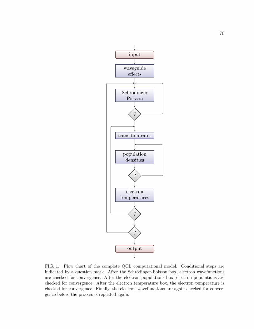
70
FIG. 1. Flow chart of the complete QCL computational model. Conditional steps areindicated by a question mark. After the Schrodinger-Poisson box, electron wavefunctionsare checked for convergence. After the electron populations box, electron populations arechecked for convergence. After the electron temperature box, the electron temperature ischecked for convergence. Finally, the electron wavefunctions are again checked for conver-gence before the process is repeated again.
71
slab waveguide model was used, which coupled the field coefficients with the axial
wavenumber via a transfer-matrix approach, which is described in detail by Baird.82
The total waveguide loss, confinement factor and gain threshold were then found.
Transition rates were calculated using Fermi’s “golden rule” for electron-photon
(e-p), electron-longitudinal-optical phonon (e-LO), and electron-electron (e-e) scat-
tering (see Sections 2.2.h, 2.2.i and 2.2.j, respectively). These rates were averaged
over the in-plane wavevector assuming Fermi-Dirac statistics. All possible transi-
tions within three periods of the active region were found, which included a four-
dimensional matrix of rates to describe all possible e-e scattering events. The effect
of screening on e-e scattering rates was also taken into account (see Section 2.2.k).
A set of iterative rate equations were then solved (see Section 2.2.l) for each
subband in order to modify the subband population densities using the calculated
transition rates as described by Donovan.62 The rate equations took into account
every transition within three periods of the active region which could possibly affect
the subband populations. This was a refinement over rate equation models which
simply used the current density to account for scattering into and out of the lasing
transition as done by Kohler.83 Once the electron and photon population densities
reached convergence, the energy balance condition was applied to determine subband
electron temperatures (see Section 2.2.m). This required calculating scattering rates
and population densities at a number of different electron temperatures, until the
temperature convergence condition was met.
Finally, after the first iteration of the complete multi-subband SCEB model, the
72
electron population densities were checked for convergence by comparing them to the
results of the previous iteration. If the densities differed by more then a predefined
threshold value, the model was repeated, starting with the Schrodinger-Poisson solver,
using the results of the previous iteration to improve the input parameters. If the
populations differed by less than the threshold value on the next iteration of the
model, then the output parameters were determined, such as lasing frequency, power
and current.
2.2.a Non-uniform Location Grid
A quantum cascade laser consists of a stack of nanoscale epitaxial semiconductor
planar layers. The material is uniform and near-infinite in the directions transverse
to crystal growth (the x and y dimensions). As a result, all of the properties in a QCL
depend only on the growth direction (the z dimension). Because the material changes
in the growth direction, all material properties, such as the dielectric constant and
effective mass, are functions of z and cannot be treated as constant. The conduction
band edge, the built-in potential, the electron wavefunctions, and the space charge are
all functions of z. In order to solve the physical equations numerically, every function
of z must be represented as a set of values over a discrete grid of z location points.
Practicality, efficiency, and accuracy dictate that all properties that are functions of
z should be defined across the same grid of points. The model therefore establishes
a location grid data structure before solving any physical equations. The location of
all z points is held fixed through-out the entire QCL computation and all variables
73
are calculated at these z points.
Create Location Grid
Three repeated periods of the core QCL structure are used in the model. While
a typical QCL has over 70 periods, three periods are sufficient for computations if
periodic boundary conditions are enforced. (The potential is not strictly periodic
because there is a net potential drop across one period due to the applied bias. More
accurately, all of the variables are periodic after the bias has been divided out.)
Multiple periods are needed to represent the structure with any reasonable amount
of accuracy since many electron wavefunctions are longer than one period. In order
to enforce periodicity and avoid edge effects, all variables are solved across all three
periods, and then the more accurate values in the central period are copied to the
outer periods.
The location grid starts at z = 0, marking the point where electrons begin
cascading down the structure, and extends to z = 3L, where L is the length of one
period. The positive z direction is the direction of the electrons’ net motion as they
cascade down through the structure.
One option for choosing location grid points is to simply distribute them uni-
formly between the endpoints according to some user-defined density. This option
would allow standard integration techniques such as Simpson’s rule to be used, as
well as simplify the numerical representation of differential equations. However, this
option leads to poor accuracy. The inaccuracy occurs because material layer widths in
74
a QCL are highly non-uniform, and the wavefunctions depend strongly on the layer
widths. Therefore, using a uniform grid of z points would require rounding layer
interface locations to the nearest grid point, significantly altering their widths, and
therefore degrading all subsequent calculations.
An alternative option is used by the present computational model: grid points
are set exactly at the location of every material layer interface. Grid points are then
spread uniformly within each layer according to a density specified by the user. By
using this approach, the grid is very close to uniform, but still preserves the exact
layer widths. Because the grid is non-uniform, the non-uniform trapezoidal method
must be used to perform numerical integrations over z instead of Simpson’s rule.
Also, when expanding differential equations, the step size h of any derivative depends
on the location and is not a constant.
Populate Grid with Material Properties
All of the position-dependent properties that stay constant are calculated at the start
of the computational model. These properties are essentially material properties
that are assumed to behave as in bulk. The band-gap, band alignment, and the
donor ionization density are discussed elsewhere. All other material properties are
calculated at each grid point using a linear model such as:
m = m0 +m1x (181)
Here x is the alloy concentration at the grid point, m0 is the property value when
there is no alloy present, and m1 is the property value change that occurs at a full
75
alloy concentration.
2.2.b Initial Fermi Levels
The first time the individual Fermi levels are calculated (see Section 2.1.e for the
derivation), the populations have not yet been determined. As an initial set of values
from which the model can iteratively converge, all of the populations are set to be
equal and then normalized so that the total of all the populations equals the overall
crystal electron density. This is based on the assumption that the electrons are
uniformly distributed across all of the states as an initial setting.
2.2.c Poisson Equation
The fourth-order Runge-Kutta (RK4) numerical method was used to solve the Poisson
equation (see Section 2.1.b for derivation). This method requires transforming one
second-order differential equation into two coupled first-order differential equations.
Applying this to Poisson’s equation we define:
dΦ(z)
dz=
1
ε(z)Φ2(z) where
dΦ2(z)
dz= −ρ(z). (182)
Boundary Conditions
This method requires knowledge of the initial conditions Φ(z0) and Φ2(z0). Instead,
the boundary conditions Φ(z0) = 0 and Φ(zN) = ∆Vbias are known. The variable
∆Vbias is the external bias voltage applied across the grid of location points (three
periods in the current model). In order to get around this problem, the shooting
76
method is used. This involves guessing some value for Φ2(z0), computing the entire
function corresponding to this value using the methods above, then computing the
error as the difference between the resulting boundary value and the desired boundary
condition. The value of Φ2(z0) is then refined using a binary search method until the
error is minimized.
2.2.d Space Charge Density
The Poisson equation (see Section 2.2.c) depends on the space charge present. How-
ever, charge density is a dynamic quantity in a QCL and special care must be taken
throughout the computational model to ensure that it is properly calculated and im-
plemented. A derivation of the various quantities described below can be found in
Section 2.1.d.
Initial Space Charge Electron Density
The populations are found using the rate equations, but when the model begins, the
rate equations have not yet been applied. An initial space charge density must be
used so that the model has a starting point before it converges to the true solution. In
theory, the choice of initial electron density should be irrelevant to the final solution.
In practice, using an initial electron density that is close to the final solution will
dramatically reduce run-time and will lessen the effects of compounding numerical
error. The model used for the initial space charge electron density is one that assumes
the electrons tend to bunch up behind the largest barrier, but extend backwards
somewhat from this barrier because of thermal smearing. The model therefore carries
77
out the following algorithm:
• Find the space charge donor density ndonor(z).
• Find the location of the thickest barrier in the QCL core structure.
• Set up the initial space charge electron density profile as a decaying exponential
curve nelec(z) = f(z) with a peak at the barrier, extending uphill away from the
barrier (in the opposite direction from the cascading electron motion).
• Scale the electron density profile until the area under its curve matches the area
under the donor density profile curve to ensure the overall total charge of the
QCL is zero, according to:
∫nelec(z)dz =
∫ndonor(z)dz. (183)
• Find the total charge density as the sum of the donor and electron densities,
according to:
ρ(z) = endonor(z)− enelec(z). (184)
• Using this initial charge density, find the built-in potential using the Poisson
equation, add the built-in potential to the conduction band-edge potential to
get the total potential, insert this into Shrodinger’s equations and find the
wavefunctions.
• Refine the initial charge density profile by using the wavefunctions multiplied
78
by the exponential model:
nelec(z) = f(z)
1 period∑i
|ψi(z)|2, (185)
and again scale to proper magnitude.
• The refined initial charge density is then the starting point when the main
iterative loop of the model is begun. For all further iterations, the populations
are found using the rate equations and applied as described in Section 2.1.d.
2.2.e Schrodinger Equation
The fourth-order Runge-Kutta (RK4) method was used to numerically solve the
Schrodinger equation (see Section 2.1.a for a derivation and Section 2.1.c for an expla-
nation of V (z)). First, the single second-order differential equation must be broken
into two first-order differential equations before applying the RK4 method:
dψ(z)
dz= m∗(z)ψ2(z) (186)
dψ2(z)
dz= − 2
~2(E − V (z))ψ(z). (187)
Boundary Conditions
This method requires the initial conditions ψ(z0) and ψ2(z0)to be known. However,
the boundary conditions that are known are ψ(z0) = 0 and ψ(zlast) = 0. Therefore
the initial conditions ψ(z0) = 0 and ψ2(z0) = 1 are used, understanding that the
entire wavefunction will be off by an overall scale factor. This scale factor error goes
away however when the wavefunction is normalized at the end to ensure that there
79
is 100% probability of finding the electron anywhere in its wavefunction. The ac-
tual boundary conditions that should be implemented are pseudo-periodic boundary
conditions because a typical QCL has over 100 repetitions of the same core period
structure. However, periodic boundary conditions are difficult to implement directly
without requiring substantial computational cost. Instead, the Dirichlet boundary
conditions are applied, and solved for the wavefunctions across three periods of the
QCL core structure. After finding all valid wavefunctions, all wavefunctions with a
center of mass that lies in the outer periods are thrown away, and all wavefunctions
with a center of mass in the central period are copied to the outer periods for future
use. This process ensures periodic boundary conditions.
Eigenvalues
These equations depend on the energy E of the electron in its state, but E is not
known beforehand. There are actually several possible solutions to a certain poten-
tial: the eigenstate wavefunctions ψn of the system, each with its own energy En. The
correct eigenenergies En are the ones that yield valid bound wavefunctions; wavefunc-
tions that do not blow up towards infinity outside the wells. Initially, a En must be
guessed, and the corresponding wavefunction must be calculated using the algorithm
listed above. The guess is then iteratively refined for En by minimizing the error in
the wavefunction. Because the wavefunction is supposed to match the boundary con-
dition ψ(zlast) = 0, the actual amplitude squared at the boundary |ψ(zlast)|2 is taken
as the error. By calculating a sweep of possible En values and their corresponding
80
wavefunction errors, an error landscape is generated. The correct energies are the
minima in such an energy landscape. The minima are identified, and then refined
using a binary search method.
Normalization
Electron wave functions should always be normalized before being used in any sub-
sequent calculations. The wave functions should not be magnitude squared unless
explicitly required, as the complex phase of the wavefunction is needed is some subse-
quent calculations. The squared wave functions constitute a probability density, thus
the proper way to normalize each is by integrating.
Defining ψnorm(z) = Aψunnorm(z) and applying the concept that the probability
of being found anywhere is 1 leads to:
1 =
∫ ∞−∞|ψnorm(z)|2dz
1 =
∫ ∞−∞
A2|ψunnorm(z)|2dz
A =1√∫∞
−∞ |ψunnorm(z)|2dz
ψnorm(z) =ψunnorm(z)√∫∞
−∞ |ψunnorm(z)|2dz(188)
The integral is done numerically using the non-uniform-grid trapezoidal method. The
integral cannot be done over infinity, but is instead done over the three periods of
the QCL core structure used in this model. Note that the location points z and
the wavefunctions are defined on a non-uniform grid in order to preserve material
layers widths exactly. Using a non-uniform grid means that traditional numerical
81
integration methods such as Simpson’s rule and the Boole rule cannot be used.
2.2.f Copy Wavefunctions
In order to strictly ensure periodic boundary conditions and periodic wavefunctions,
but still model three full periods of the core structure, the wavefunctions in the central
period are copied to the outer periods and replace the original wavefunctions there.
Even though the wavefunctions typically extend across multiple periods, most of the
wavefunction is contained in one period, and is therefore assigned to that period by
calculating the location of the center of mass of the wavefunction. All wavefunctions
with a center of mass lying outside the central period are discarded, and then all
remaining wavefunctions are copied and shifted left one period, and copied again and
shifted right one period. The wavefunctions are shifted in space by the length of one
period and shifted in energy by the potential energy drop across one period due to
the bias.
Note that when some wavefunctions are copied to the outer periods, part of the
wavefunction’s profile extends into regions not modeled by the three-period grid of
location points and therefore must be discarded. The natural result is that such
wavefunctions are no longer accurately normalized and are also unable to give accu-
rate form factors. Such edge effects are inevitable but have minimal overall effect.
These edge effects are minimized by always keeping only calculations performed in
the central period and copying them to the outer periods for every type of calcula-
tions. Using outer periods keeps the edge effects away from the central period where
82
the meaningful calculations are performed. Additionally, wavefunctions that reside
in the central period still extend into the outer periods.
Calculating Center of Masses
A given wavefunction ψi(z) corresponding to the ith energy level has some spatial
extent. If instead of treating its square as the quantum extent of one electron, it is
treated as the population density of a large ensemble of electrons, then it becomes
the spatially varying electron density of that level. Because the electrons all have the
same mass (neglecting the fact that the effective mass varies from material layer to
layer), the center of mass of the ith state is:
zi,com =
∫|ψi(z)|2zdz∫|ψi(z)|2dz
. (189)
The wavefunctions are properly normalized as soon as they are found, so that the
integral in the denominator is equal to one:
zi,com =
∫|ψi(z)|2zdz. (190)
The integral is done numerically using the non-uniform-grid trapezoidal method. The
integral cannot be done over infinity, but is instead done over the three periods of
the QCL core structure used in this model. Note that the location points z and
the wavefunctions are defined on a non-uniform grid in order to preserve material
layers widths exactly. Using a non-uniform grid means that traditional numerical
integration methods such as Simpson’s rule cannot be used.
Every time new wavefunctions are found using the Schrodinger equation, the
model immediately calculates the center of mass of each wavefunction, assigns it to
83
one of the three periods based on this center of mass, copies the central wavefunctions
to the outer periods, and provides this information for use by later calculations.
Equivalent Levels
After copying wavefunctions to the outer periods, all periods have been forced to
be numerically equivalent. Every wavefunction in an outer period matches exactly
with one in the central period. This information is used later on to optimize the rate
equations as well as the scattering rate calculations. For this reason, all wavefunctions
in the three periods are indexed in order of energy, the lowest energy being state zero.
A list of equivalent wavefunctions according to index number is kept for later use.
In this sense, the wavefunctions are automatically matched because we have forced
them to be matched.
2.2.g Waveguide Numerical Analysis
The equations which were derived in Section 2.1.f require numerical methods in order
to solve them. The problem is to solve for Ai and Bi in each region in terms of the
known permittivities εi, boundary locations xi, frequency ω and the guessed wave
number kz. The wave number kz is guessed and refined until the outermost boundary
conditions are met, that of fields approaching zero at positive and negative infinity
for x.
Add the two boundary condition equations together to eliminate Bi+1 and solve
84
for Ai+1:
Ai+1 =1
2
(1 +
kx,iεi+1
kx,i+1εi
)Aie
i(kx,i−kx,i+1)xi+1
2
(1− kx,iεi+1
kx,i+1εi
)Bie
−i(kx,i+kx,i+1)xi . (191)
Subtract the two equations to eliminate Ai+1 and solve for Bi+1:
Bi+1 =1
2
(1− kx,iεi+1
kx,i+1εi
)Aie
i(kx,i+kx,i+1)xi+1
2
(1 +
kx,iεi+1
kx,i+1εi
)Bie
−i(kx,i−kx,i+1)xi . (192)
This now gives a set of iteration equations. Using a trial kz and because ω, εi, and
µi are known, kx,i is also known using:
kx,i =√εiµiω2 − k2z . (193)
Thus if A0 and B0 are known, all other Ai and Bi are found using these iteration
equations.
Since the bound modes are the modes of interest, the wave must die down to
zero at negative and positive infinity. This leads to the conditions:
• if =(kx,0) > 0, then A0 = 0
• if =(kx,0) < 0, then B0 = 0
• if =(kx,N) < 0, then AN = 0
• if =(kx,N) > 0, then BN = 0
There is an overall normalization constant for the mode that needs to be found
and applied after the problem is solved. This is done by setting the non-zero coefficient
of the zeroth layer equal to one and normalizing it at the end to its proper value.
85
• if =(κ0) < 0, then A0 = 1
• if =(κ0) > 0, then B0 = 1
The system is solved iteratively for the propagation constant kz. First a guess for
kz is made (or a grid of guesses), then the iteration equations are applied to find the
fields everywhere corresponding to this kz. The amount that the coefficients AN and
BN in the last region differ from what they should be as dictated by the boundary
conditions is calculated as the error corresponding to that kz. The right kz is found
by refining its value until the error is minimized. The lowest-order mode is the one of
most importance and it is the one that is found. Note that kz is complex-valued so
that finding the physical modes amounts to finding the minima in a two-dimensional
error landscape.
Final Numerical Recipe
1. Calculate the complex permittivity of each layer using the Drude model (see
Section 2.1.f) and assume non-magnetic material µi = µ0.
2. Sweep across a grid of initial possible values for the real and imaginary part of
the wave vector kz:
(a) For each complex kz value, calculate the complex x-directional wave num-
ber of each waveguide layer using:
kx,i =√εiµiω2 − k2z (194)
86
(b) Set A0 and B0 according to the following rule:
• if =(kx,0) > 0, then A0 = 0 and B0 = 1
• else A0 = 1 and B0 = 0
(c) Calculate all remaining Ai and Bi using:
Ai+1 =1
2
(1 +
kx,iεi+1
kx,i+1εi
)Aie
i(kx,i−kx,i+1)xi
+1
2
(1− kx,iεi+1
kx,i+1εi
)Bie
−i(kx,i+kx,i+1)xi
Bi+1 =1
2
(1− kx,iεi+1
kx,i+1εi
)Aie
i(kx,i+kx,i+1)xi
+1
2
(1 +
kx,iεi+1
kx,i+1εi
)Bie
−i(kx,i−kx,i+1)xi (195)
(d) Find the error as the difference between the calculated AN or BN and the
required AN or BN according to:
• if =(kx,N) < 0, then AN = 0
• else BN = 0
3. Find all mimima in the 2D error landscape as a function of kz. A minima is a
grid point where its error value is lower than the error value of its eight nearest
neighbors.
4. Refine every minimum kz by repeating step 2 for additional guesses and keeping
the ones that give the least error. Use the method of gradient descent. Step
iteratively in the opposite direction of the gradient of the error landscape ac-
cording to: [kz]n+1 = [kz]n− γn∇f([kz]n) where f(kz) is the 2D error landscape
87
as a function of kz. Due to the complexity of the error landscape, the gradient
cannot be solved analytically but the finite difference is used. The step size γn
is optimized by finding the first value that minimizes f([kz]n+1) locally.
5. Choose the kz which corresponds to the lowest-order mode. It is the one with
the lowest value for (kx/kz) in the largest layer.
6. Once the lowest order kz has been identified and refined, use step 2 again to get
the final values for Ai and Bi
7. Using the final values of Ai and Bi calculate all the fields across a fine grid of
x locations using:
Hy,i(x) = Aieikx,ix +Bie
−ikx,ix
Ex,i(x) =kzωεi
(Aieikx,ix +Bie
−ikx,ix)
Ez,i(x) =kx,iωεi
(−Aieikx,ix +Bie−ikx,ix)
|Hi(x)|2 = |Hy,i(x)|2
|Ei(x)|2 = |Ex,i(x)|2 + |Ez,i(x)|2 (196)
8. Calculate the confinement factor for this waveguide structure at this frequency
using the trapezoidal or cubic splines method:
Γ =
∫act. reg.
|Ex,i(x)|2dx∫∞−∞ |Ei(x)|2dx
(197)
9. Calculate the associated parameters:
(a) Waveguide Loss: αw = 2=(kz)
88
(b) Total Cavity Loss: α = αw + αM1 + αM2
(c) Threshold Gain: gth = α/Γ
(d) Velocity: v = ω<(kz)
(e) Effective Index of Refraction: n = cv
(f) Total Cavity Photon loss rate: Wp = αv
(g) Total Cavity Photon lifetime: τp = 1/Wp
10. Repeat Steps 1 through 9 for many possible frequencies in order to generate
look-up tables.
Cutoff Frequency
Upon generating the look-up tables, which essentially establish loss vs. frequency
and confinement factor vs. frequency trend lines, a problem arises. Below a certain
cutoff frequency, electromagnetic modes cannot propagate. In terms of the practical
requirements, the waveguide model should return a confinement factor of zero and
a loss of infinity for these frequencies. However, the waveguide model is designed to
find modes as minima in an error landscape, and cannot find the lack of modes. As
implemented above, the waveguide model will output erroneous values for frequencies
below cutoff, and the rest of the model will use these values as if valid, leading to
widespread error.
The solution is to have the model determine the cutoff frequency and then hard-
set all confinement factors to zero and all losses to infinity below this frequency. Note
89
that if the confinement factor is set to zero, then divide-by-zero errors will occur later
on in the rate equations. In practice, each confinement factor must be set below cutoff
to a very small non-zero number; so small that it is essentially zero. Similarly, the
losses below cutoff cannot be set to infinity in a numerical calculation. Instead each
loss is set equal to a very high number that essentially behaves as infinity.
The cutoff frequency is found by starting at a high frequency on the confinement
factor vs. frequency curve, and asymptotically finding at what frequency the curve
approaches zero confinement.
2.2.h Photon Scattering Implementation
The photon scattering rate into a narrow mode distribution from Eq. (71) is calculated
without the photon number factor. The photon number is then found using the rate
equations. Note that there is great uncertainty in the literature as to what the
pure dephasing time T ∗2 should be,27,41,71 which is used to determine the line width.
The value used and published for mid-infrared QCL’s was found to give poor results
for Terahertz QCL’s. The value of T ∗2 = 15 picoseconds was found to give the best
model predictions for Terahertz QCL’s when compared to experiment and is the value
currently used by the model.
The integral in the oscillator strength of Eq. (72) is done numerically using the
non-uniform-grid trapezoidal method. The integral cannot be done over infinity, but
is instead done over the three periods of the QCL core structure used in this model.
90
2.2.i Phonon Scattering Numerical Implementation
The form factor integrands of Eq. (84) (see Section 2.1.h) are defined over a non-
uniform grid, so their integrals are done using the non-uniform trapezoidal method.
The rest of the integrals in Eq. (83) are defined on a uniform grid, so they are
calculated using Simpson’s rule or the Bode (Boole) rule. The form factor integrals are
performed over the full three periods of the QCL structure. The wavenumber integral
runs from zero to the maximum wavenumber possible. The maximum wavenumber is
the one corresponding to the well height in energy space, because wavenumbers greater
than this are not confined in the quantum well structures and do not contribute to
the process.
2.2.j Electron-Electron Computational Implementation
The two approaches (as discussed at the end of Section 2.1.i) were found to give
similar results with regards to numerical accuracy. The relative wavevector approach
was chosen because it was simpler to implement and is the only one considered in the
rest of this thesis. Also, state-blocking was found to be negligible in terahertz QCL’s
(see Section 4.2). For this reason, the final states are assumed to be empty so that
ff = 0 and fg = 0. Upon dropping state blocking, it was found that nothing else
depends on kf or kg. For this reason, they do not need to be calculated.
Since electron-electron scattering is a four-body interaction, the number of scat-
tering events which have to be calculated scales as N4, where N is the number of
states in a structure. These events include both symmetric types such as 2, 2→ 1, 1
91
(where 2 and 1 represent subbands) and asymmetric types such as 3, 2→ 2, 1. Previ-
ous studies have indicated the importance of these asymmetric scattering events (see
works by Donovan, Kinlser and Lee84–86) and are discussed further in Section 4.2.
The steps which are employed when calculating electron-electron scattering rates
are as follows:
• Calculate the form factor A(q) look-up table for a large set of q points using
the non-uniform trapezoidal method:
A(q) =
∫ Lz
0
dz
∫ Lz
0
dz′ψ∗f (z)ψ∗g(z′)ψi(z)ψj(z
′)e−|z−z′|q. (198)
• Calculate the front constant:
C =1∫
kifi(ki)dk i
m∗e4
64π3ε2~3(199)
• Calculate the energy difference constant:
g20 =4m∗
~2[Ei(0) + Ej(0)− Ef (0)− Eg(0)] (200)
• Calculate the scattering rate by performing the integrals and calling a sub-
routine to calculate the innermost integral. The integrals are calculated over a
uniform grid of points. The user chooses between 10 to 1000 points per integral,
depending on the accuracy desired. Experience has shown that using more than
50 integration points per integral has no discernible effect on the final results
of the entire computational model. The wavenumber integrals are calculated
from a lower limit of zero to an upper limit of kmax, which corresponds to the
92
height of the energy barriers. Any electrons with energies beyond the barrier
height will not be contained in the quantum wells. The angular integrals are
performed over the whole unit circle. Because the integrals are defined over
uniform grids, standard methods such Simpson’s Rule or the Boole (Bode) rule
are used. The scattering rate is in the form:
Wi,j→f,g = C
∫dkikifi(ki)
∫dkjkjfj(kj)
∫dθijU(ki, kj, θij ) (201)
• Calculate the inner integral U by performing the following steps:
1. Calculate the quantity: k2u = kikj cos θij
2. Calculate the quantity: g2 = k2j + k2i − 2k2u (If g = 0 then W = 0 for this
set of integration points)
3. Calculate the quantity: q = 12
√g20 + 2g2 − 2g
√g20 + g2 cos θ (If g20 +g2 ≤ 0
then W = 0 for this set of integration points)
4. Use these quantities to find: U(ki, kj, θij ) =∫dθ∣∣∣A(q)q ∣∣∣2
Additional Computational Optimizations
When including all antisymmetric transitions, calculating the form factor look-up
tables becomes unreasonably time intensive. For instance, a structure with 30 levels
across the three periods will require 304 = 810, 000 look-up tables to cover all possible
interactions of the states i, j to f , g. However, the number of calculations to perform
is reduced if redundant calculations are skipped.
93
Because of the periodic nature of the QCL structure, transitions completely
happening in the first period are identical to those happening solely in the second
period. If every wavefunction is located to either period 1, 2, or 3 based on its
center of mass (period 3 being the lowest in energy), then all redundant calculations
are skipped by applying the following rules. Later on, the whole data structure is
populated by copying the original data to its appropriate redundant locations. The
notation used below is ij → fg so that for instance 11 → 23 means an electron in
period 1 scatters with another electron in period 1 and they end up in periods 2 and
3 respectively.
• Include all 22→ 22 transitions.
• Skip transitions if: i 6= 1 and j 6= 1 and f 6= 1 and g 6= 1.
• Skip all 11→ 11 transitions.
• Skip double period transitions, when |i− f | = 2 or |j − g| = 2.
Scrutiny of the form factor equation reproduced below reveals that there are
several symmetries:
A(q) =
∫ Lz
0
dz
∫ Lz
0
dz′ψ∗f (z)ψ∗g(z′)ψi(z)ψj(z
′)e−|z−z′|q (202)
Aijfg = Afjig = Aigfj = Ajigf = Ajfgi = Agijf = Agfji = Afgij (203)
The way to skip these redundancies computationally is through the following rules.
Skip every transition except when (indexes now refer to subbands):
94
• j ≤ g
• i ≤ j and i ≤ f and i ≤ g
• f ≤ g if i = j.
Note that the data structure must be all filled out in order for later use, so these
rules must be used to copy the unique data to its corresponding redundant locations.
Also note that these symmetries only apply to the form factor and not the entire e-e
scattering rate.
2.2.k Electron-electron screening implementation
In order to take into account screening of the electron-electron interaction, the di-
electric constant ε in Eq. (118) is replaced by a modified form, which is a function of
the transition wavevector q, as described in Section 2.1.j. Since this quantity is no
longer a constant, it must be brought inside the integral which averages over ki before
arriving at Eq. (118). This is accomplished by making a look-up table for values of
q, similar to the one made for the form factor A(q) (see Section 2.2.j). In fact, the
permittivity look-up table uses the form factor look-up table since it is comprised of
not only the polarization function and a 1/q term, but also the intrasubband form
factor term Aiiii(q). Therefore, the inclusion of scattering requires a modified version
of the computational model to calculate the ki average integral.
The actual form of the dielectric function implemented was a modified version
of the single subband screening model. Single subband models only consider the
95
polarization of the electrons in the initial state of the e-e interaction, such as the one
employed by Smet.53 However, the modified form takes into account all subbands
within one period of the QCL active region. Additionally, the modified form of the
model has been shown by Lu and Jirauschek to provide better agreement with the full
screening tensor equation (see Eq. (138) from Section 2.1.j) than the single subband
model.73,74 This modified model is represented as Eq. (149), which was derived at the
end of Section 2.2.k. As done in that section, the temperature-dependent polarization
function of Maldague60 was found in the static limit as in Ando’s paper.61 The
polarization integral of Eq. (150) is computed numerically over a uniform grid using
standard methods such as Simpson’s rule or the Bode (Boole) rule.
2.2.l Rate Equation Implementation
In order to determine the population densities for the electron subband states, a
rate equation approach was implemented. This method determines the populations
through an iterative solution to a set of coupled equations. Each equation has the
form of Eq.(157). However, since these equations are all coupled to one another, the
system of population densities is under-specified so the additional equation:
∑i
ni = N, (204)
must be used, where i represents an electron subband and N represents the total
charge density.
In order to implement iteration equations some initial values for the electron
population densities and photon population densities must be chosen. The closer
96
that the initial values are to the final values, the more quickly the solutions will
converge. For the initial electron densities, all are set equal so that total electron
density is evenly divided among the levels. For the photon populations, an arbitrary
number is chosen that has the right order of magnitude as experimental values, such
as 1018 photons/m3.
The iterative solution of these electron rate equations is as follows:
• Initially set all populations equal to one another based on the total charge
density of the system
• Calculate the populations for each subband using Eq. (157)
• Normalize the populations so that they satisfy Eq. (204)
• Recalculate and normalize the populations using Eqs. (157) and (204)
• Repeat until the populations do not change more than a pre-defined threshold
value between multiple iterations
Together, the photon and electron population equations form another layer of
coupled equations. However, simply applying Eqs. (157) and (161) does not lead to
a converging solution as the parameter space shape is not conducive to convergence.
The solution, however, is forced to converge by taking the previous photon population
values and moving them slowly towards the photon population calculated by the above
equation, instead of setting them outright equal to the photon population calculated
by the above equation. What happens in practice is that through the course of
97
the numerical iterative process, the electron population inversion temporarily goes
higher than it ever would in the real laser. If the equation above is applied blindly,
the photon density will go negative for high population inversions and unphysical
trends will result. In reality, the population inversion asymptotically approaches a
“pinned” value. To handle this numerically, the above equation is applied and if the
photon population goes negative, the previous photon population was too low, so it
is increased in the next iteration. In real QCL’s, the stimulated emission of photons
depletes the upper level enough that it never goes passed the pinned value.
2.2.m Multi-subband SCEB Algorithm
As described in Section 2.1.l, the electron temperatures must be determined to pro-
vide a more accurate description of the dynamics within a QCL. As described in that
section, these temperatures can deviate significantly from the lattice temperature
of the device and can vary between subbands as well. However, previous publica-
tions expressed difficulties associated with generating a set of electron temperatures
reliably using the self-consistent energy balance approach such as in the paper by
Ikonic.79 Therefore, an original algorithm and an associated convergence condition
was developed to determine the electron temperature for each subband, as described
below.
• Initially, the electron temperatures were all assumed to be equal to the lattice
temperature, TL. All calculations were performed (such as the scattering rates
and population densities) based on this assumption. Then, Eq. (168) was cal-
98
culated for each subband. This resulted in an energy transition rate for each
subband, which was typically non-zero.
• Since the magnitude of the energy transition rate was assumed to be an in-
dication of how far the current subband electron temperature was from the
correct temperature, the value of the energy transition was used to generate a
new guess for the subband temperatures. For the first several iterations of this
algorithm, the new temperatures were generated by multiplying each subband
energy transition rate by a constant factor.
• Once a new set of subband temperatures was generated, these temperatures
were used to recalculate the transition rates and subband population densities.
Then, Eq. (168) was calculated for each subband again, which resulted in a new
set of subband energy transition rates. The same factor used in the previous
iteration of the algorithm was used again to generate a new set of temperatures
from the current values of the energy transition rates.
• After several iterations of this algorithm, the data from the previous iterations
were used to generate new temperature estimates more intelligently. Specifically,
the temperatures and energy transition rates for each subband were used to
create a “slope” rather than an arbitrary constant factor:
∆(dEf/dt)
∆Tf. (205)
This slope was multiplied with the current value of the energy transition rate
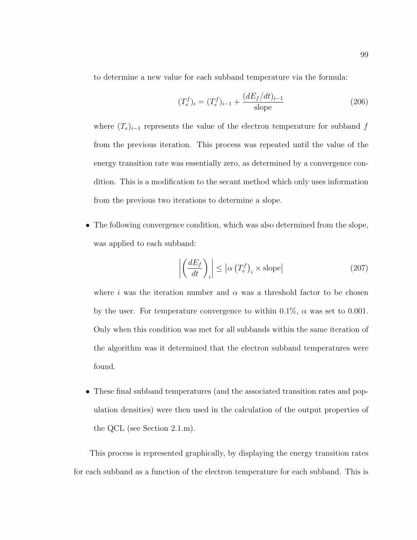
99
to determine a new value for each subband temperature via the formula:
(T fe )i = (T fe )i−1 +(dEf/dt)i−1
slope(206)
where (Te)i−1 represents the value of the electron temperature for subband f
from the previous iteration. This process was repeated until the value of the
energy transition rate was essentially zero, as determined by a convergence con-
dition. This is a modification to the secant method which only uses information
from the previous two iterations to determine a slope.
• The following convergence condition, which was also determined from the slope,
was applied to each subband:∣∣∣∣(dEfdt)i
∣∣∣∣ ≤ ∣∣α (T fe )i × slope∣∣ (207)
where i was the iteration number and α was a threshold factor to be chosen
by the user. For temperature convergence to within 0.1%, α was set to 0.001.
Only when this condition was met for all subbands within the same iteration of
the algorithm was it determined that the electron subband temperatures were
found.
• These final subband temperatures (and the associated transition rates and pop-
ulation densities) were then used in the calculation of the output properties of
the QCL (see Section 2.1.m).
This process is represented graphically, by displaying the energy transition rates
for each subband as a function of the electron temperature for each subband. This is
100
-4
-2
0
2
4
6
40 80 120 160 200 240
ener
gytr
ansi
tion
rate
(×10
12
J/s
)
electron temp. (K)
12345
FIG. 2. The energy transition rates for each subband as a function of electron temperaturefor each subband. The five subbands shown are those from the 1.8 THz Kumar structure.All subband temperatures start at the lattice temperature of 150 K (as indicated by thevertical dashed line) and end when the energy transition rate reaches zero (as indicated bythe horizontal dashed line).
shown in Fig. 2, where the subband energy transition rates are those from a study of
a 1.8 THz QCL designed by Kumar.16
2.2.n Average Electron Temperature Implementation
The previous section discussing the multi-subband electron temperature algorithm
deals with the temperatures for each subband individually. This method required
finding these temperatures after several convergence conditions were met simultane-
ously. This condition is simplified if there is not a need for every subband temperature
to be determined. An average electron temperature is determined, which describes
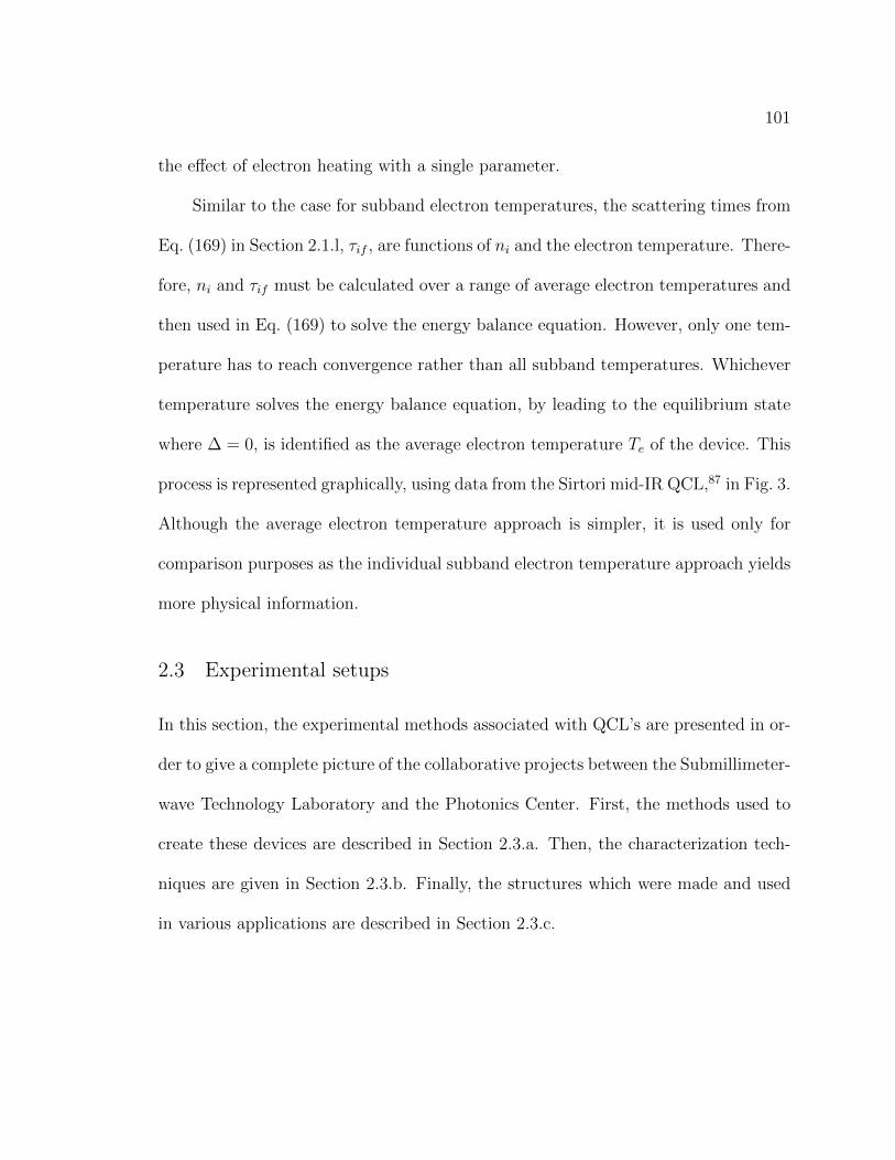
101
the effect of electron heating with a single parameter.
Similar to the case for subband electron temperatures, the scattering times from
Eq. (169) in Section 2.1.l, τif , are functions of ni and the electron temperature. There-
fore, ni and τif must be calculated over a range of average electron temperatures and
then used in Eq. (169) to solve the energy balance equation. However, only one tem-
perature has to reach convergence rather than all subband temperatures. Whichever
temperature solves the energy balance equation, by leading to the equilibrium state
where ∆ = 0, is identified as the average electron temperature Te of the device. This
process is represented graphically, using data from the Sirtori mid-IR QCL,87 in Fig. 3.
Although the average electron temperature approach is simpler, it is used only for
comparison purposes as the individual subband electron temperature approach yields
more physical information.
2.3 Experimental setups
In this section, the experimental methods associated with QCL’s are presented in or-
der to give a complete picture of the collaborative projects between the Submillimeter-
wave Technology Laboratory and the Photonics Center. First, the methods used to
create these devices are described in Section 2.3.a. Then, the characterization tech-
niques are given in Section 2.3.b. Finally, the structures which were made and used
in various applications are described in Section 2.3.c.
102
FIG. 3. Plot of total energy change ∆ as a function of electron temperature for a typicalconfiguration, showing the correct electron temperature as the one at the zero crossing. Inthis case, Te = 83 K. Also shown are the contributions from phonon emission (ph em),phonon absorption (ph abs) and electron-electron scattering (e-e) to the energy balanceequation. These data are calculated for the Sirtori mid-IR structure at a bias voltage of 48kV/cm and at a lattice temperature of 77 K.
2.3.a QCL production methods
As a typical example of how devices are made, run number 238 will be described
from start to finish. This particular wafer was grown using the active region design
of Vitiello.88 More details about this and other designs can be found in Section 2.3.c.
The QCL active regions were grown using molecular beam epitaxy (MBE), a
process by which layers of material are deposited mono-layers at a time until a desired
thickness is reached. To start, a GaAs buffer of 500 nm was grown on top of a Si
substrate, which took approximately 2000 seconds. On top of this, a GaAs bottom
contact layer, which was n+ doped with Si at a concentration of 2×1018 cm−3 was
grown to a thickness of 600 nm. Then a 16 nm thick GaAs layer, n− doped with Si
103
at a concentration of 5×1017 cm−3, was grown. Both of these layers together took
approximately 2400 seconds to grow.
On top of these layers the active region design was grown. This consisted of 90
periods of the design, with each period consisting of 18 layers of varying thickness.
The exact dimension of each layer can be found in Vitiello’s paper.88 The layers
alternated between GaAs and AlGaAs, where the Al alloy concentration was 15%.
Also, two of the GaAs layers were doped using Si to a concentration of 1.6×1016 cm−3.
However, it should be noted that when this laser was completed, it was discovered
that the active region layers were grown 3.5% thicker than the original design.
On top of the active region a GaAs top contact layer, which was n+ doped with
Si at a concentration of 5×1018 cm−3 was grown to a thickness of 80 nm. Finally,
a GaAs cap was grown with n++ doping to a thickness of 3.5 nm. Both of the top
layers together took approximately 320 seconds to grow. The thickness from the top
of the wafer surface to the bottom contact layer was measured to be 11.3 µm.
Fabrication techniques varied slightly between devices and especially between
the two different types of waveguides: semi-insulating surface plasmon (SISP) and
metal-metal (MM). However, all structures discussed in this thesis were made using
SISP waveguides and, as a typical example of this fabrication process, run number
238 will be described.
After cleaning, the first photolithography step began with baking the wafer at
110◦C for five minutes and allowed to cool for five minutes. Photoresist (AZ1512)
was spun at 2000 rpm for 30 seconds and then baked on a hot plate at 95◦C for two
104
minutes and then allowed to cool for five minutes. To form a ridge, the sample was
then developed (AZ327) for 1 minute 55 seconds, and then rinsed in de-ionized (DI)
water and hard baked for five minutes.
Next, the wet etching process consisted of applying H3PO4:H202:H2O (1:2:20) at
170 rpm’s for 26 minutes, which produced an etch depth of 12 µm. For the second
photolithography step, the pre-baking was done as in the first step but the photoresist
(P4620) was spun at 5000 rpm for 30 seconds. After baking at 95◦C for 2 minutes
and cooling for five minutes, the sample was developed for 4 minutes 55 seconds using
AZ400K. The sample was dipped in Chlorobenzene for 15 minutes and blown dry with
N2. It was then developed for 8 minutes using AZ400K, then rinsed in DI and blown
dry with N2 again.
Then, the metal deposition process was begun by dipping into 50% HCl for 15
seconds and then rinsing in DI water and blow drying with N2. E-beam deposition
was then performed with Ni (50 A), Ge (170 A), Au (330 A), Ni (150 A), and then
Au (3000 A). An ultrasonic bath with acetone was then used for lift off for 5 seconds.
After blow drying with N2, the sample was annealed at 425◦C for 150 seconds.
The final step in completing this sample was the packaging process. Thinning
was preformed by first grinding using SiC and then polishing with Alumina. Back
side metal deposition was then done with Ti (150 A) and Au (1000 A). Lastly, the
sample was cleaved to give a ridge length of 3.5 mm using a wafer scriber.
105
2.3.b Device characterization methods
Once the wafer growth and fabrication processes were completed, characterization of
the QCL’s could take place. This was typically done through a series of standard
measurements, (as described in Danylov’s thesis89) such as: the device current versus
voltage (IV ), the output optical power versus current (LI), and the emission spectra.
Lasers were characterized in both pulsed and cw mode and each sample was mounted
on the cold finger of a liquid helium (LHe) dewar. The LHe held the laser temperature
to about 5-20 K when the sample was not driven. The QCL’s were centered on a
1-inch-diameter high-density polyethylene (HDPE) external window of the dewar,
which was approximately 25 mm from the facet of the QCL.
The output power from the devices was measured by a LHe cooled silicon (Si)
bolometer. The windows of the QCL dewar and the bolometer were aligned and posi-
tioned next to each other to minimize any power loss. The bolometer was calibrated
against a Keating photo-acoustic power meter to measure the bolometer responsivity,
which was then used to calculate the output power.
In pulsed mode, lasers were driven with a high power pulse generator (Agilent
8114A) using square wave pulses with a frequency of 30 Hz, and a pulse width of
1 ms. The QCL current and voltage signals were digitized with a data acquisition
board (DAQ) NI 6212. The output voltage of the QCL was recorded by the bolometer
and read by the lock-in amplifier (LIA) SR830. The LIA was triggered with a signal
from the QCL driver. Finally, the bolometer signal was then converted to output
power using the measured bolometer responsivity. The QCL current, voltage, and
106
bolometer signal were recorded and stored on a computer. The IV , LI, and dV/dI
versus I relationships were then determined. Characterization of QCL’s in cw mode
was very similar to that for pulsed mode except for the use of a chopper and the LIA,
which was triggered with pulses from the chopper controller.
Spectra were obtained using a FTIR spectrometer Bruker 66vs with an evacu-
ated spectrometer box. This reduced the effects of atmospheric absorption due to
water vapor. To measure the QCL emission spectra in cw mode, the rapid-scan mod-
ulation regime of the spectrometer was used. In this regime, the translating mirror
was moved continuously over some distance, depending on the resolution, to gener-
ate an interferogram. A fast Fourier transform (FFT) was then performed on the
interferogram to obtain a source spectrum.
To measure the QCL emission spectra in pulsed mode, step-scan modulation of
the spectrometer was used. In this regime, the translating mirror moved in steps,
pausing after each step to record the intensity through a LIA. After a certain number
of steps, the interferogram was collected and then, after performing a FFT, a spectrum
was produced. However, since one high resolution scan took approximately 30 minutes
to complete and there was little gained from recording spectral content in pulsed
mode, spectra were measured mainly in cw mode.
2.3.c Details of grown devices
In the following tables are data which describe some of the growth and fabrication
runs of lasing QCL’s. All of the QCL’s here are of the bound-to-continuum type
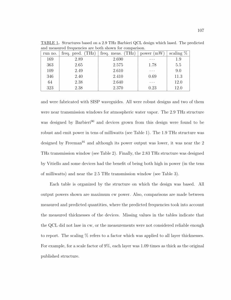
107
TABLE 1. Structures based on a 2.9 THz Barbieri QCL design which lased. The predictedand measured frequencies are both shown for comparison.
run no. freq. pred. (THz) freq. meas. (THz) power (mW) scaling %
169 2.89 2.690 · · · 1.9
363 2.65 2.575 1.78 5.5
109 2.49 2.610 · · · 9.0
346 2.40 2.410 0.69 11.3
64 2.38 2.640 · · · 12.0
323 2.38 2.370 0.23 12.0
and were fabricated with SISP waveguides. All were robust designs and two of them
were near transmission windows for atmospheric water vapor. The 2.9 THz structure
was designed by Barbieri90 and devices grown from this design were found to be
robust and emit power in tens of milliwatts (see Table 1). The 1.9 THz structure was
designed by Freeman91 and although its power output was lower, it was near the 2
THz transmission window (see Table 2). Finally, the 2.83 THz structure was designed
by Vitiello and some devices had the benefit of being both high in power (in the tens
of milliwatts) and near the 2.5 THz transmission window (see Table 3).
Each table is organized by the structure on which the design was based. All
output powers shown are maximum cw power. Also, comparisons are made between
measured and predicted quantities, where the predicted frequencies took into account
the measured thicknesses of the devices. Missing values in the tables indicate that
the QCL did not lase in cw, or the measurements were not considered reliable enough
to report. The scaling % refers to a factor which was applied to all layer thicknesses.
For example, for a scale factor of 9%, each layer was 1.09 times as thick as the original
published structure.
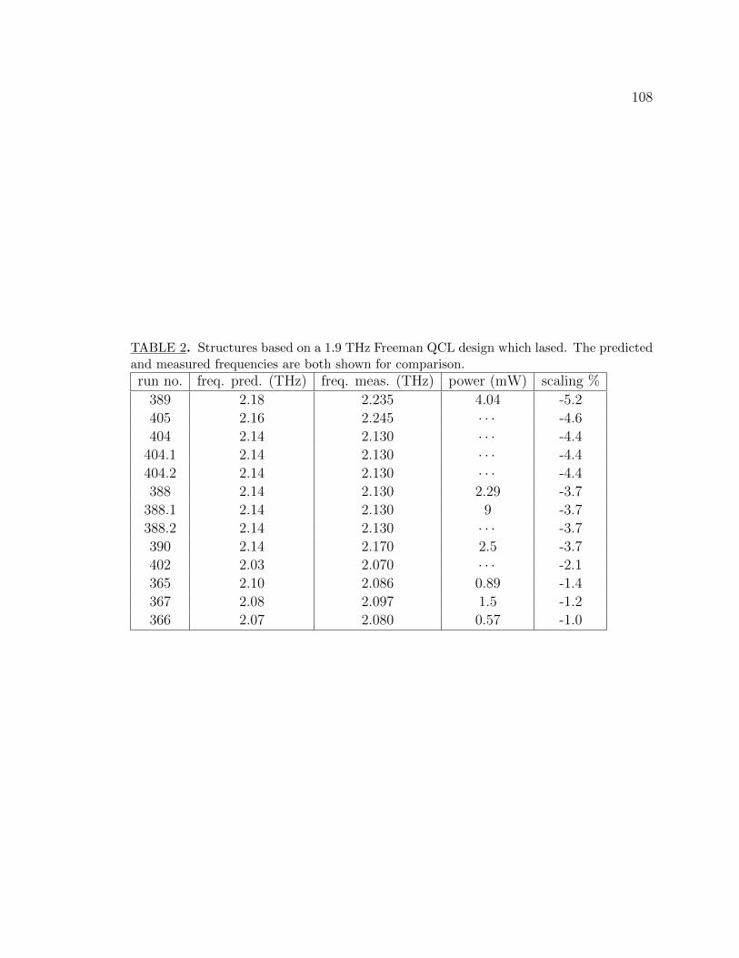
108
TABLE 2. Structures based on a 1.9 THz Freeman QCL design which lased. The predictedand measured frequencies are both shown for comparison.
run no. freq. pred. (THz) freq. meas. (THz) power (mW) scaling %
389 2.18 2.235 4.04 -5.2
405 2.16 2.245 · · · -4.6
404 2.14 2.130 · · · -4.4
404.1 2.14 2.130 · · · -4.4
404.2 2.14 2.130 · · · -4.4
388 2.14 2.130 2.29 -3.7
388.1 2.14 2.130 9 -3.7
388.2 2.14 2.130 · · · -3.7
390 2.14 2.170 2.5 -3.7
402 2.03 2.070 · · · -2.1
365 2.10 2.086 0.89 -1.4
367 2.08 2.097 1.5 -1.2
366 2.07 2.080 0.57 -1.0
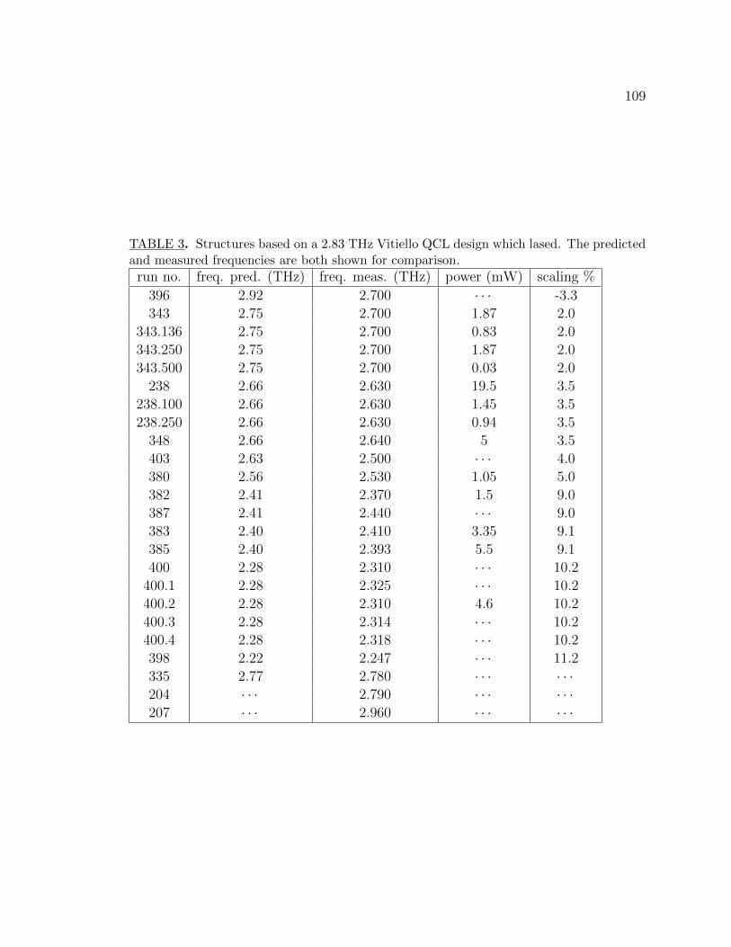
109
TABLE 3. Structures based on a 2.83 THz Vitiello QCL design which lased. The predictedand measured frequencies are both shown for comparison.
run no. freq. pred. (THz) freq. meas. (THz) power (mW) scaling %
396 2.92 2.700 · · · -3.3
343 2.75 2.700 1.87 2.0
343.136 2.75 2.700 0.83 2.0
343.250 2.75 2.700 1.87 2.0
343.500 2.75 2.700 0.03 2.0
238 2.66 2.630 19.5 3.5
238.100 2.66 2.630 1.45 3.5
238.250 2.66 2.630 0.94 3.5
348 2.66 2.640 5 3.5
403 2.63 2.500 · · · 4.0
380 2.56 2.530 1.05 5.0
382 2.41 2.370 1.5 9.0
387 2.41 2.440 · · · 9.0
383 2.40 2.410 3.35 9.1
385 2.40 2.393 5.5 9.1
400 2.28 2.310 · · · 10.2
400.1 2.28 2.325 · · · 10.2
400.2 2.28 2.310 4.6 10.2
400.3 2.28 2.314 · · · 10.2
400.4 2.28 2.318 · · · 10.2
398 2.22 2.247 · · · 11.2
335 2.77 2.780 · · · · · ·204 · · · 2.790 · · · · · ·207 · · · 2.960 · · · · · ·
110
III. RESULTS
The following sections present the results from various studies which either mod-
ified or implemented the computational model. Only background information and
data are given here, as detailed explanations of the implications of these studies are
explained in the Discussion section.
3.1 Average Electron Temperature
As originally published by Harrison,67 the method of finding an average electron
temperature was based on the use of 15 states in 3/2 periods of the QCL active region.
However, this is an odd choice for multiple reasons. First, since this temperature is
an average, by using 3/2 periods, more weight is given to the states which fall into the
extra 1/2 period when the average is calculated. Second, if more of the active region
is included in the QCL computations it is unclear what fraction of the active region
should be used in average Te calculations. Additionally, if only 3/2 periods are used,
it is unclear which combination of electron states should be used to make up those
3/2 periods. In order to resolve these issues, a study was conducted to observe the
effects of using different combinations of states to calculate the electron temperature.
As explained in the following paragraphs, it was found that these calculations were
sensitive to such combinations.
First, an attempt was made to recreate the theoretical results presented by Har-
rison.67 This work studied a mid-IR QCL structure by Sirtori87 referred to in this
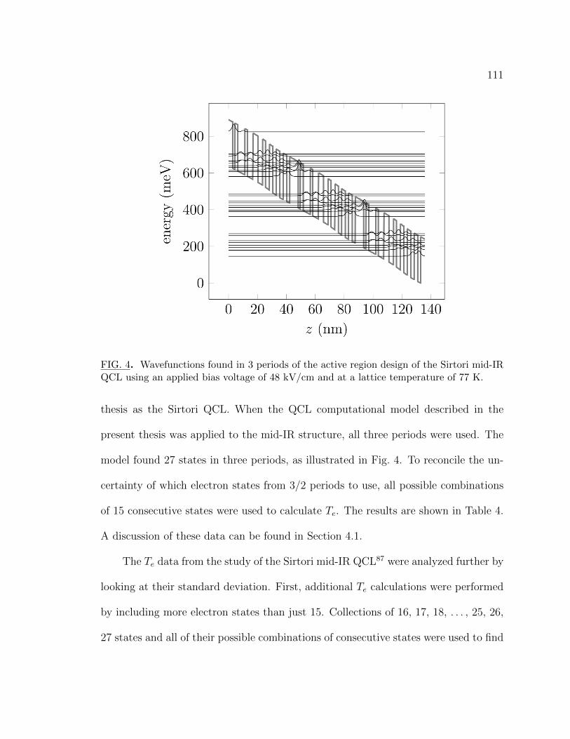
111
FIG. 4. Wavefunctions found in 3 periods of the active region design of the Sirtori mid-IRQCL using an applied bias voltage of 48 kV/cm and at a lattice temperature of 77 K.
thesis as the Sirtori QCL. When the QCL computational model described in the
present thesis was applied to the mid-IR structure, all three periods were used. The
model found 27 states in three periods, as illustrated in Fig. 4. To reconcile the un-
certainty of which electron states from 3/2 periods to use, all possible combinations
of 15 consecutive states were used to calculate Te. The results are shown in Table 4.
A discussion of these data can be found in Section 4.1.
The Te data from the study of the Sirtori mid-IR QCL87 were analyzed further by
looking at their standard deviation. First, additional Te calculations were performed
by including more electron states than just 15. Collections of 16, 17, 18, . . . , 25, 26,
27 states and all of their possible combinations of consecutive states were used to find
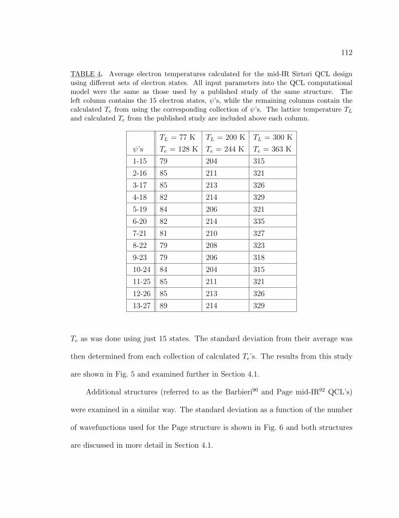
112
TABLE 4. Average electron temperatures calculated for the mid-IR Sirtori QCL designusing different sets of electron states. All input parameters into the QCL computationalmodel were the same as those used by a published study of the same structure. Theleft column contains the 15 electron states, ψ’s, while the remaining columns contain thecalculated Te from using the corresponding collection of ψ’s. The lattice temperature TLand calculated Te from the published study are included above each column.
TL = 77 K TL = 200 K TL = 300 K
ψ’s Te = 128 K Te = 244 K Te = 363 K
1-15 79 204 315
2-16 85 211 321
3-17 85 213 326
4-18 82 214 329
5-19 84 206 321
6-20 82 214 335
7-21 81 210 327
8-22 79 208 323
9-23 79 206 318
10-24 84 204 315
11-25 85 211 321
12-26 85 213 326
13-27 89 214 329
Te as was done using just 15 states. The standard deviation from their average was
then determined from each collection of calculated Te’s. The results from this study
are shown in Fig. 5 and examined further in Section 4.1.
Additional structures (referred to as the Barbieri90 and Page mid-IR92 QCL’s)
were examined in a similar way. The standard deviation as a function of the number
of wavefunctions used for the Page structure is shown in Fig. 6 and both structures
are discussed in more detail in Section 4.1.
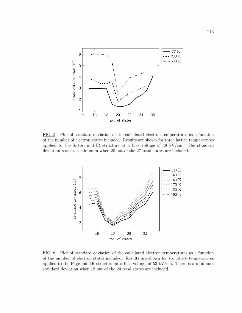
113
FIG. 5. Plot of standard deviation of the calculated electron temperatures as a functionof the number of electron states included. Results are shown for three lattice temperaturesapplied to the Sirtori mid-IR structure at a bias voltage of 48 kV/cm. The standarddeviation reaches a minimum when 20 out of the 27 total states are included.
FIG. 6. Plot of standard deviation of the calculated electron temperatures as a functionof the number of electron states included. Results are shown for six lattice temperaturesapplied to the Page mid-IR structure at a bias voltage of 53 kV/cm. There is a minimumstandard deviation when 18 out of the 24 total states are included.
114
In order to make comparisons with experimental measurements, the Page QCL,92
was studied in more detail. The lattice and electron temperatures of the Page QCL
have been measured experimentally and reported by Spagnolo80 where measurements
were made over a range of electronic power. However, the voltages used were well
below the alignment voltage. Two different heat sink temperatures (TH), 140 K and
243 K, were also used. Comparisons were made between the Te’s calculated using
the 3 period computational model and the reported measurements. Specifically, the
design was simulated using the highest values of electric power quoted in the paper
at both heat sink temperatures. At TH = 140 K, the highest power used was 7 W.
At this point, the measured TL was 190 K and the measured Te was 295 K. When
simulated with the 3 period QCL computational model, the calculated Te was found
to be 192 K. At TH = 243 K, the highest power used was 3 W. At this point the
measured TL was 265 K and the measured Te was 330 K. When simulated, the Te was
found to be 270 K.
The Page structure was also modeled using bias voltages above threshold. A
range of lattice temperatures were used for each bias voltage and the electron tem-
peratures were calculated under these conditions (see Fig. 7). This study is discussed
in Section 4.1.
3.2 The effect of approximations on e-e scattering rates
Electron-electron scattering is an essential transport mechanism for electrons in a
QCL. Therefore, the electron-electron scattering rates must be calculated between all
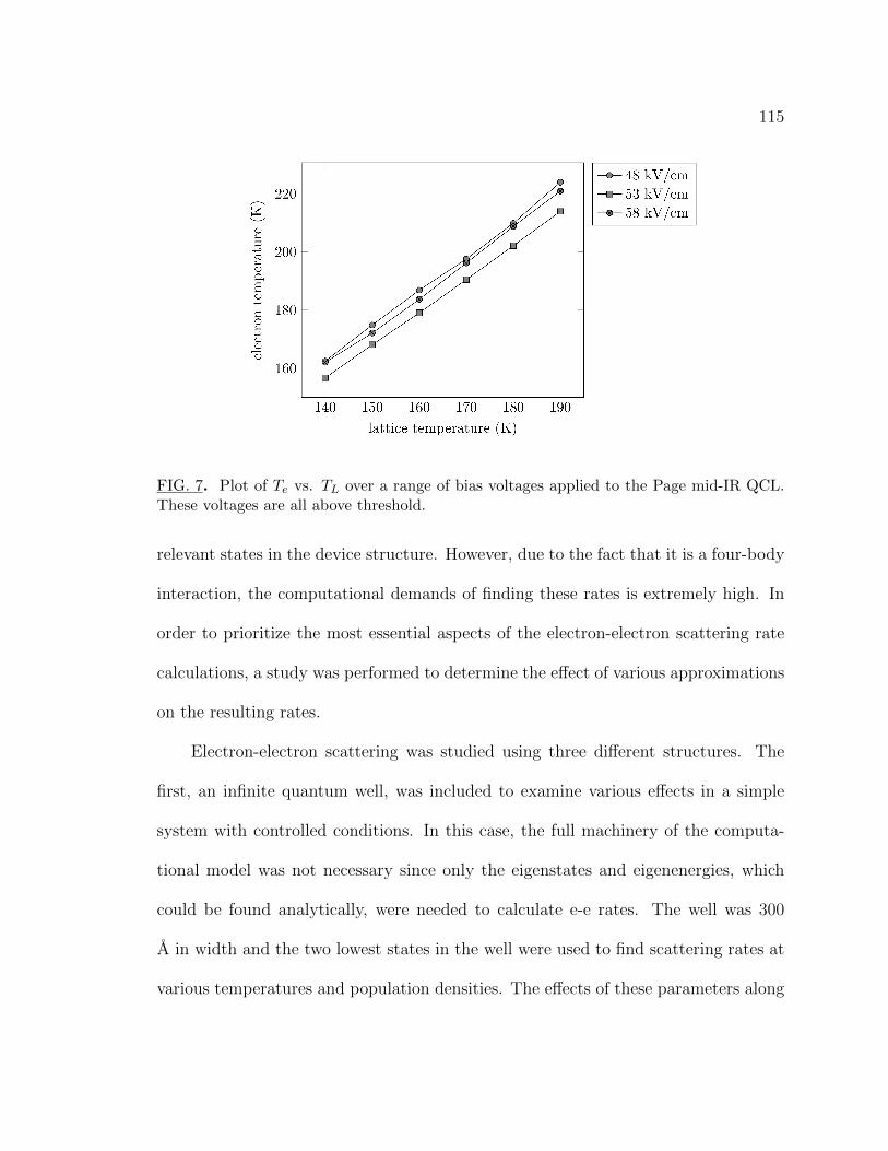
115
FIG. 7. Plot of Te vs. TL over a range of bias voltages applied to the Page mid-IR QCL.These voltages are all above threshold.
relevant states in the device structure. However, due to the fact that it is a four-body
interaction, the computational demands of finding these rates is extremely high. In
order to prioritize the most essential aspects of the electron-electron scattering rate
calculations, a study was performed to determine the effect of various approximations
on the resulting rates.
Electron-electron scattering was studied using three different structures. The
first, an infinite quantum well, was included to examine various effects in a simple
system with controlled conditions. In this case, the full machinery of the computa-
tional model was not necessary since only the eigenstates and eigenenergies, which
could be found analytically, were needed to calculate e-e rates. The well was 300
A in width and the two lowest states in the well were used to find scattering rates at
various temperatures and population densities. The effects of these parameters along
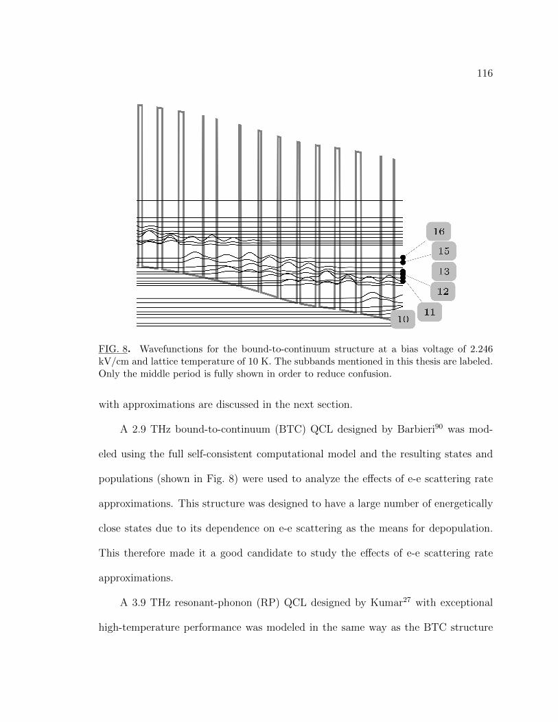
116
FIG. 8. Wavefunctions for the bound-to-continuum structure at a bias voltage of 2.246kV/cm and lattice temperature of 10 K. The subbands mentioned in this thesis are labeled.Only the middle period is fully shown in order to reduce confusion.
with approximations are discussed in the next section.
A 2.9 THz bound-to-continuum (BTC) QCL designed by Barbieri90 was mod-
eled using the full self-consistent computational model and the resulting states and
populations (shown in Fig. 8) were used to analyze the effects of e-e scattering rate
approximations. This structure was designed to have a large number of energetically
close states due to its dependence on e-e scattering as the means for depopulation.
This therefore made it a good candidate to study the effects of e-e scattering rate
approximations.
A 3.9 THz resonant-phonon (RP) QCL designed by Kumar27 with exceptional
high-temperature performance was modeled in the same way as the BTC structure
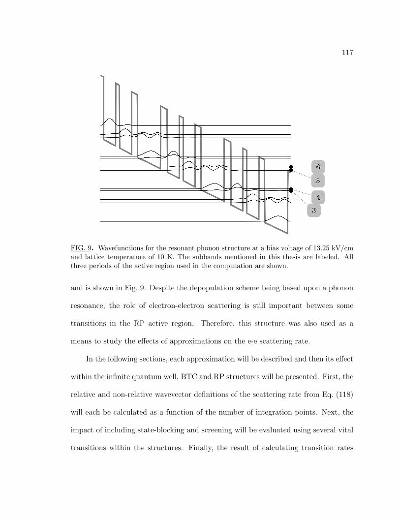
117
FIG. 9. Wavefunctions for the resonant phonon structure at a bias voltage of 13.25 kV/cmand lattice temperature of 10 K. The subbands mentioned in this thesis are labeled. Allthree periods of the active region used in the computation are shown.
and is shown in Fig. 9. Despite the depopulation scheme being based upon a phonon
resonance, the role of electron-electron scattering is still important between some
transitions in the RP active region. Therefore, this structure was also used as a
means to study the effects of approximations on the e-e scattering rate.
In the following sections, each approximation will be described and then its effect
within the infinite quantum well, BTC and RP structures will be presented. First, the
relative and non-relative wavevector definitions of the scattering rate from Eq. (118)
will each be calculated as a function of the number of integration points. Next, the
impact of including state-blocking and screening will be evaluated using several vital
transitions within the structures. Finally, the result of calculating transition rates
118
other than the symmetric type (i, i→ f, f) will be presented.
3.2.a Convergence and integration types
In order to numerically implement the integrals in Eq. (118), the step size for each
integration has to be chosen. The mean scattering rate equations consist of four nested
integrals (not including the sum over states in the denominator and not including the
two integrals in the form factor, which are pre-calculated). Therefore, if the step
size along each integration axis is defined so that there are 100 points, then the total
number of integration points used to find the scattering rate is 1004 = 108. Deciding
whether to use more or less points is a compromise between speed and accuracy and
requires some consideration.
As more points are used, the e-e rate eventually converges to some value. How-
ever, if this convergence can be reached more quickly, then fewer integration points
are necessary to achieve a certain level of accuracy. The behavior of the integrals in
Eq. (118) was studied as a function of the number of integration points to see whether
the non-relative wavevector or the relative wavevector form reached convergence with
fewer points. This was done for the infinite quantum well, the BTC structure and
the RP structure.
The scattering rate as a function of the number of integration points is shown in
Fig. 10 for the infinite quantum well at one particular temperature and population
density. The data are discussed in Section 4.2.
In order to make a general statement about the relative performance of the inte-
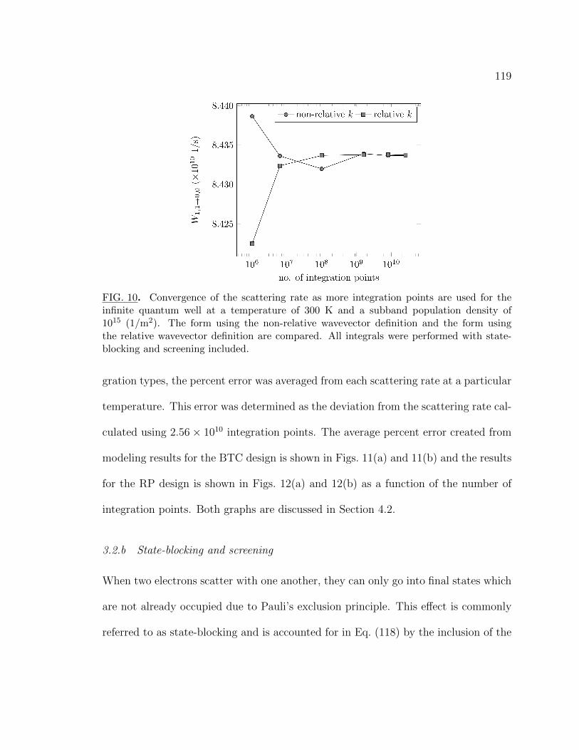
119
FIG. 10. Convergence of the scattering rate as more integration points are used for theinfinite quantum well at a temperature of 300 K and a subband population density of1015 (1/m2). The form using the non-relative wavevector definition and the form usingthe relative wavevector definition are compared. All integrals were performed with state-blocking and screening included.
gration types, the percent error was averaged from each scattering rate at a particular
temperature. This error was determined as the deviation from the scattering rate cal-
culated using 2.56× 10¹⁰ integration points. The average percent error created from
modeling results for the BTC design is shown in Figs. 11(a) and 11(b) and the results
for the RP design is shown in Figs. 12(a) and 12(b) as a function of the number of
integration points. Both graphs are discussed in Section 4.2.
3.2.b State-blocking and screening
When two electrons scatter with one another, they can only go into final states which
are not already occupied due to Pauli’s exclusion principle. This effect is commonly
referred to as state-blocking and is accounted for in Eq. (118) by the inclusion of the
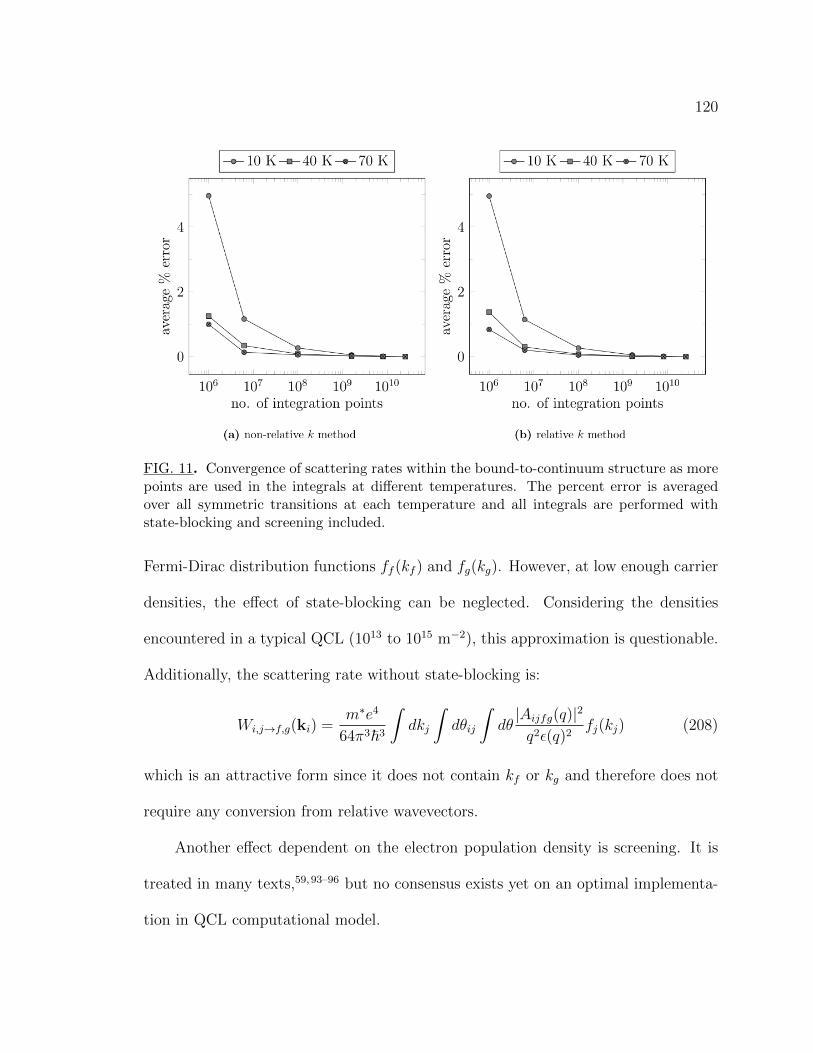
120
FIG. 11. Convergence of scattering rates within the bound-to-continuum structure as morepoints are used in the integrals at different temperatures. The percent error is averagedover all symmetric transitions at each temperature and all integrals are performed withstate-blocking and screening included.
Fermi-Dirac distribution functions ff (kf ) and fg(kg). However, at low enough carrier
densities, the effect of state-blocking can be neglected. Considering the densities
encountered in a typical QCL (1013 to 1015 m−2), this approximation is questionable.
Additionally, the scattering rate without state-blocking is:
Wi,j→f,g(ki) =m∗e4
64π3~3
∫dkj
∫dθij
∫dθ|Aijfg(q)|2
q2ε(q)2fj(kj) (208)
which is an attractive form since it does not contain kf or kg and therefore does not
require any conversion from relative wavevectors.
Another effect dependent on the electron population density is screening. It is
treated in many texts,59,93–96 but no consensus exists yet on an optimal implementa-
tion in QCL computational model.
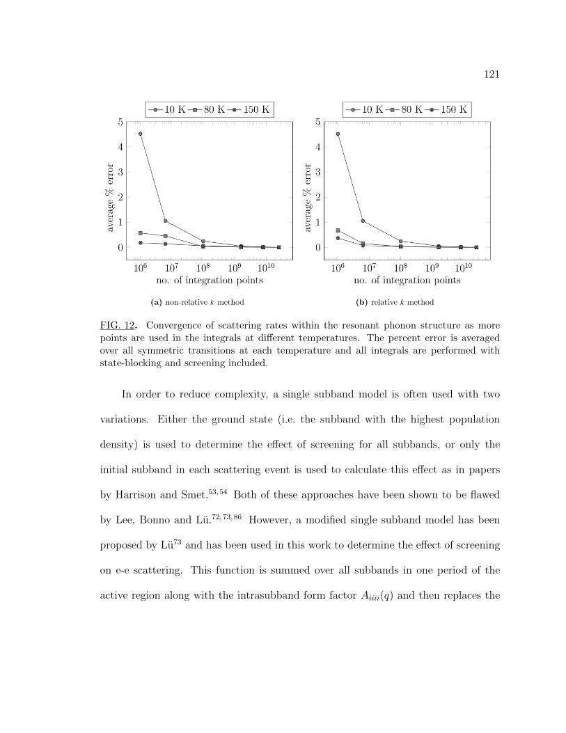
121
FIG. 12. Convergence of scattering rates within the resonant phonon structure as morepoints are used in the integrals at different temperatures. The percent error is averagedover all symmetric transitions at each temperature and all integrals are performed withstate-blocking and screening included.
In order to reduce complexity, a single subband model is often used with two
variations. Either the ground state (i.e. the subband with the highest population
density) is used to determine the effect of screening for all subbands, or only the
initial subband in each scattering event is used to calculate this effect as in papers
by Harrison and Smet.53,54 Both of these approaches have been shown to be flawed
by Lee, Bonno and Lu.72,73,86 However, a modified single subband model has been
proposed by Lu73 and has been used in this work to determine the effect of screening
on e-e scattering. This function is summed over all subbands in one period of the
active region along with the intrasubband form factor Aiiii(q) and then replaces the
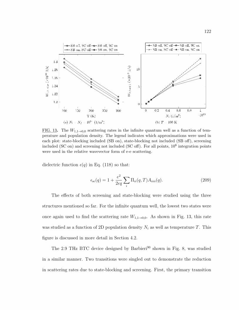
122
FIG. 13. The W1,1→0,0 scattering rates in the infinite quantum well as a function of tem-perature and population density. The legend indicates which approximations were used ineach plot: state-blocking included (SB on), state-blocking not included (SB off), screeningincluded (SC on) and screening not included (SC off). For all points, 106 integration pointswere used in the relative wavevector form of e-e scattering.
dielectric function ε(q) in Eq. (118) so that:
εsc(q) = 1 +e2
2εq
∑i
Πii(q, T )Aiiii(q). (209)
The effects of both screening and state-blocking were studied using the three
structures mentioned so far. For the infinite quantum well, the lowest two states were
once again used to find the scattering rate W1,1→0,0. As shown in Fig. 13, this rate
was studied as a function of 2D population density Ni as well as temperature T . This
figure is discussed in more detail in Section 4.2.
The 2.9 THz BTC device designed by Barbieri90 shown in Fig. 8, was studied
in a similar manner. Two transitions were singled out to demonstrate the reduction
in scattering rates due to state-blocking and screening. First, the primary transition
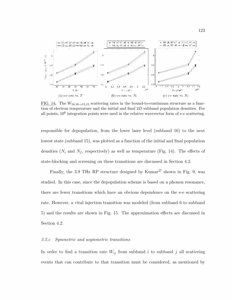
123
FIG. 14. The W16,16→15,15 scattering rates in the bound-to-continuum structure as a func-tion of electron temperature and the initial and final 2D subband population densities. Forall points, 106 integration points were used in the relative wavevector form of e-e scattering.
responsible for depopulation, from the lower laser level (subband 16) to the next
lowest state (subband 15), was plotted as a function of the initial and final population
densities (Ni and Nf , respectively) as well as temperature (Fig. 14). The effects of
state-blocking and screening on these transitions are discussed in Section 4.2.
Finally, the 3.9 THz RP structure designed by Kumar27 shown in Fig. 9, was
studied. In this case, since the depopulation scheme is based on a phonon resonance,
there are fewer transitions which have an obvious dependence on the e-e scattering
rate. However, a vital injection transition was modeled (from subband 6 to subband
5) and the results are shown in Fig. 15. The approximation effects are discussed in
Section 4.2.
3.2.c Symmetric and asymmetric transitions
In order to find a transition rate Wij from subband i to subband j all scattering
events that can contribute to that transition must be considered, as mentioned by
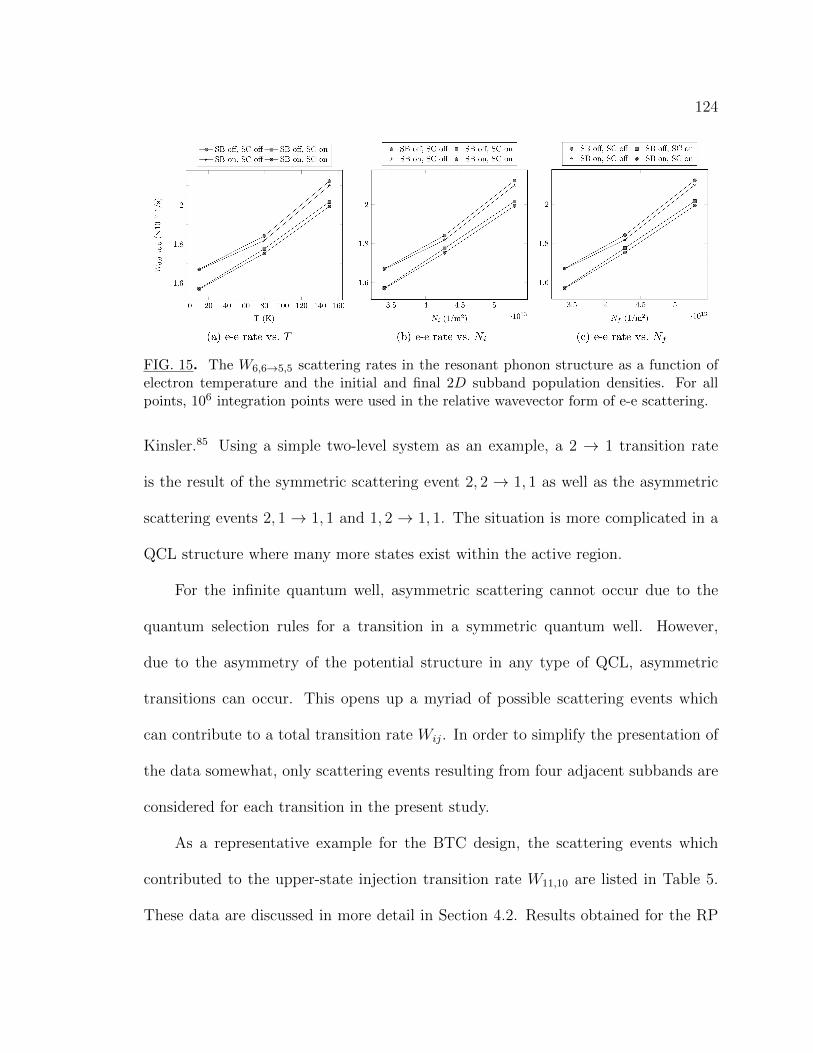
124
FIG. 15. The W6,6→5,5 scattering rates in the resonant phonon structure as a function ofelectron temperature and the initial and final 2D subband population densities. For allpoints, 106 integration points were used in the relative wavevector form of e-e scattering.
Kinsler.85 Using a simple two-level system as an example, a 2 → 1 transition rate
is the result of the symmetric scattering event 2, 2 → 1, 1 as well as the asymmetric
scattering events 2, 1 → 1, 1 and 1, 2 → 1, 1. The situation is more complicated in a
QCL structure where many more states exist within the active region.
For the infinite quantum well, asymmetric scattering cannot occur due to the
quantum selection rules for a transition in a symmetric quantum well. However,
due to the asymmetry of the potential structure in any type of QCL, asymmetric
transitions can occur. This opens up a myriad of possible scattering events which
can contribute to a total transition rate Wij. In order to simplify the presentation of
the data somewhat, only scattering events resulting from four adjacent subbands are
considered for each transition in the present study.
As a representative example for the BTC design, the scattering events which
contributed to the upper-state injection transition rate W11,10 are listed in Table 5.
These data are discussed in more detail in Section 4.2. Results obtained for the RP
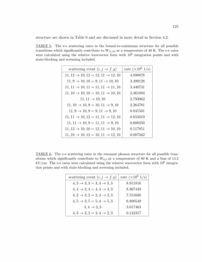
125
structure are shown in Table 6 and are discussed in more detail in Section 4.2.
TABLE 5. The e-e scattering rates in the bound-to-continuum structure for all possibletransitions which significantly contribute to W11,10 at a temperature of 40 K. The e-e rateswere calculated using the relative wavevector form with 106 integration points and withstate-blocking and screening included.
scattering event (i, j → f, g) rate (×109 1/s)
11, 12→ 10, 12 = 12, 11→ 12, 10 4.898878
11, 9→ 10, 10 = 9, 11→ 10, 10 3.499128
11, 11→ 10, 11 = 11, 11→ 11, 10 3.440731
11, 10→ 10, 10 = 10, 11→ 10, 10 3.361894
11, 11→ 10, 10 2.793062
11, 10→ 10, 9 = 10, 11→ 9, 10 2.264781
11, 9→ 10, 9 = 9, 11→ 9, 10 0.841501
11, 11→ 10, 12 = 11, 11→ 12, 10 0.655019
11, 11→ 10, 9 = 11, 11→ 9, 10 0.608250
11, 12→ 10, 10 = 12, 11→ 10, 10 0.117851
11, 10→ 10, 12 = 10, 11→ 12, 10 0.087562
TABLE 6. The e-e scattering rates in the resonant phonon structure for all possible tran-sitions which significantly contribute to W4,3 at a temperature of 80 K and a bias of 14.2kV/cm. The e-e rates were calculated using the relative wavevector form with 106 integra-tion points and with state-blocking and screening included.
scattering event (i, j → f, g) rate (×109 1/s)
4, 3→ 3, 3 = 3, 4→ 3, 3 8.911816
4, 4→ 3, 4 = 4, 4→ 4, 3 8.367449
4, 2→ 3, 2 = 2, 4→ 2, 3 7.551600
4, 5→ 3, 5 = 5, 4→ 5, 3 6.800549
4, 4→ 3, 3 3.017463
4, 3→ 3, 2 = 3, 4→ 2, 3 0.132317
126
3.3 Scaling Studies
In collaboration with the University of Massachusetts Lowell Photonics Center, a
series of structures was studied and successfully grown. These devices needed to op-
erate at specific frequencies in order to minimize the absorption of terahertz radiation
by atmospheric water vapor. These frequencies were attained by scaling pre-existing
structure designs found in the literature by a certain percentage. Structures were
chosen based on their past growth success at the Photonics Center.
One such device was a 1.9 THz QCL designed by Freeman.91 This device was
modeled over a number of scaling percentages in order to determine the proper scaling
factor to apply to the device design in order for it to emit at 1.97 THz. A smooth curve
was generated from this data by applying a spline fit to the modeling data. It should
be noted that these predictions were obtained without energy balance convergence
or population convergence effects included as they had not yet been implemented
at the time this data was generated. Also of note is that the lasing frequency at a
given scale factor depends on the applied bias. The predicted frequencies reported in
these results are for the bias originally published as the one that gave peak power,
scaled appropriately. The structure was then grown at several of these scaling factors.
The resulting devices and their associated measured scaling factors and emission
frequencies are shown in Fig. 16 along with the modeling data. Each experimental
data point in this figure represents a separately grown device. The associated run
number is labeled alongside the corresponding data point. Further information about
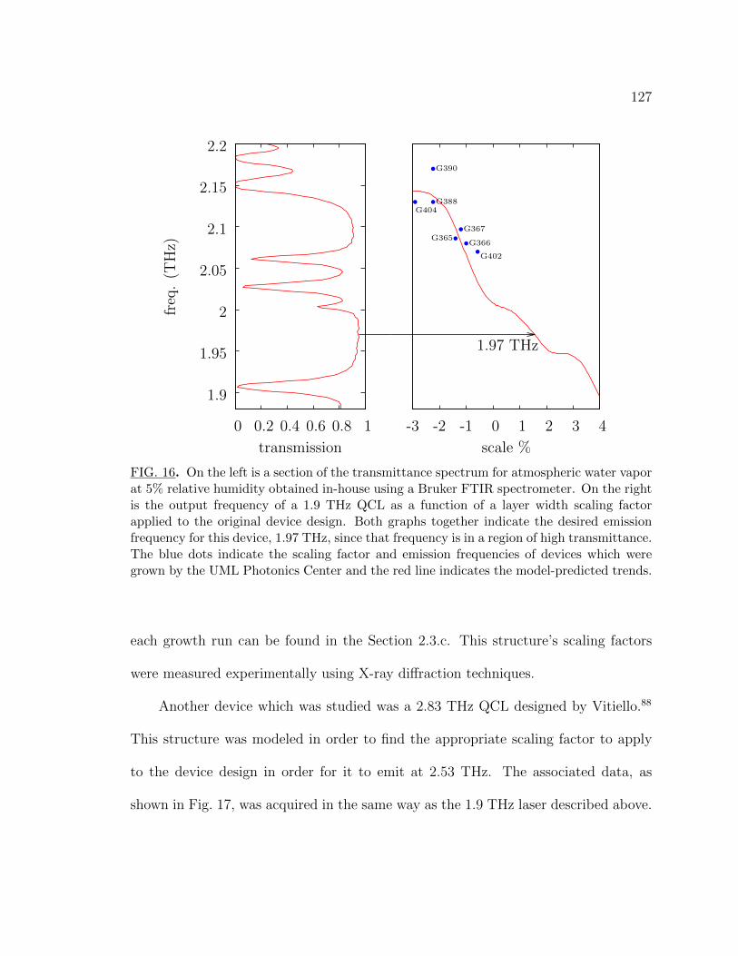
127
1.9
1.95
2
2.05
2.1
2.15
2.2
0 0.2 0.4 0.6 0.8 1
freq
.(T
Hz)
transmission
-3 -2 -1 0 1 2 3 4
scale %
1.97 THz
G404
G390
G388
G367G365
G366
G402
FIG. 16. On the left is a section of the transmittance spectrum for atmospheric water vaporat 5% relative humidity obtained in-house using a Bruker FTIR spectrometer. On the rightis the output frequency of a 1.9 THz QCL as a function of a layer width scaling factorapplied to the original device design. Both graphs together indicate the desired emissionfrequency for this device, 1.97 THz, since that frequency is in a region of high transmittance.The blue dots indicate the scaling factor and emission frequencies of devices which weregrown by the UML Photonics Center and the red line indicates the model-predicted trends.
each growth run can be found in the Section 2.3.c. This structure’s scaling factors
were measured experimentally using X-ray diffraction techniques.
Another device which was studied was a 2.83 THz QCL designed by Vitiello.88
This structure was modeled in order to find the appropriate scaling factor to apply
to the device design in order for it to emit at 2.53 THz. The associated data, as
shown in Fig. 17, was acquired in the same way as the 1.9 THz laser described above.
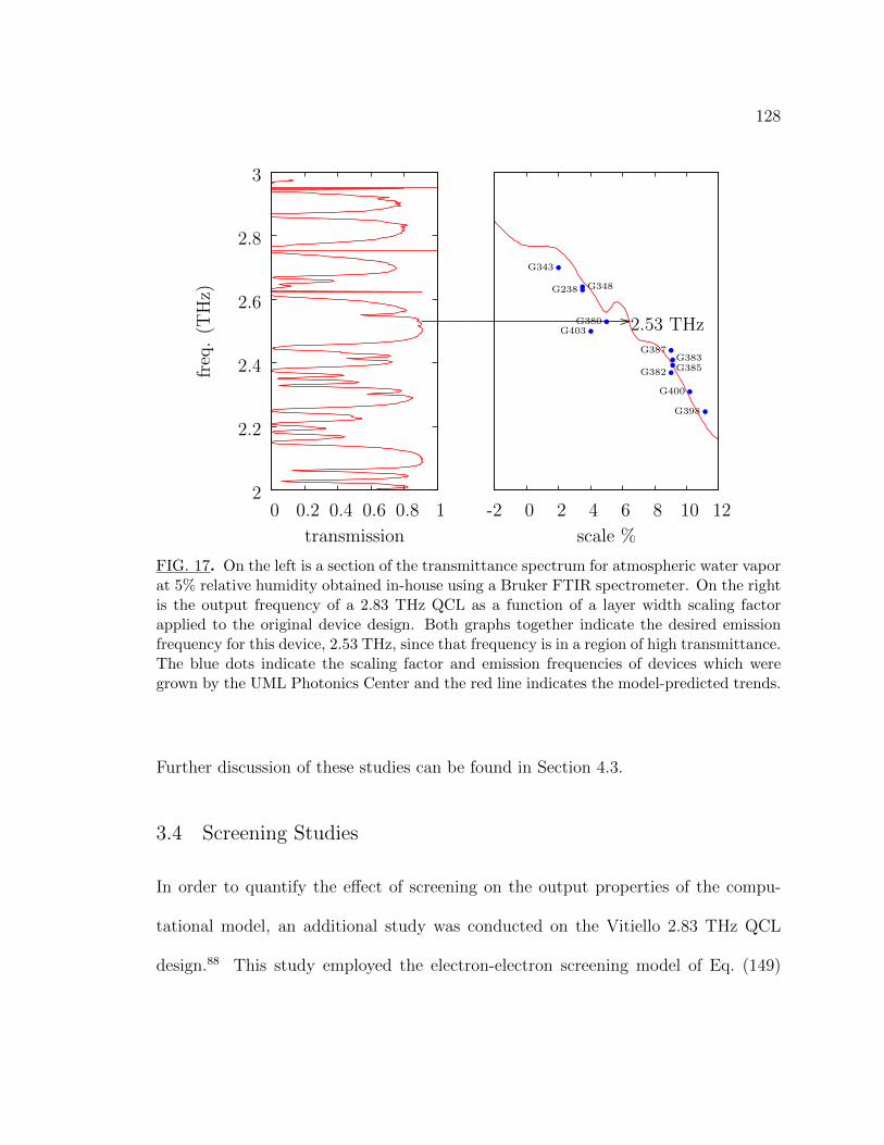
128
2
2.2
2.4
2.6
2.8
3
0 0.2 0.4 0.6 0.8 1
freq
.(T
Hz)
transmission
-2 0 2 4 6 8 10 12
scale %
2.53 THz
G343
G348G238
G403G380
G387
G382
G383G385
G400
G398
FIG. 17. On the left is a section of the transmittance spectrum for atmospheric water vaporat 5% relative humidity obtained in-house using a Bruker FTIR spectrometer. On the rightis the output frequency of a 2.83 THz QCL as a function of a layer width scaling factorapplied to the original device design. Both graphs together indicate the desired emissionfrequency for this device, 2.53 THz, since that frequency is in a region of high transmittance.The blue dots indicate the scaling factor and emission frequencies of devices which weregrown by the UML Photonics Center and the red line indicates the model-predicted trends.
Further discussion of these studies can be found in Section 4.3.
3.4 Screening Studies
In order to quantify the effect of screening on the output properties of the compu-
tational model, an additional study was conducted on the Vitiello 2.83 THz QCL
design.88 This study employed the electron-electron screening model of Eq. (149)
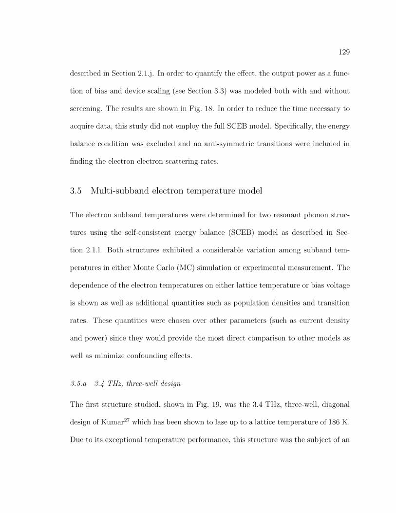
129
described in Section 2.1.j. In order to quantify the effect, the output power as a func-
tion of bias and device scaling (see Section 3.3) was modeled both with and without
screening. The results are shown in Fig. 18. In order to reduce the time necessary to
acquire data, this study did not employ the full SCEB model. Specifically, the energy
balance condition was excluded and no anti-symmetric transitions were included in
finding the electron-electron scattering rates.
3.5 Multi-subband electron temperature model
The electron subband temperatures were determined for two resonant phonon struc-
tures using the self-consistent energy balance (SCEB) model as described in Sec-
tion 2.1.l. Both structures exhibited a considerable variation among subband tem-
peratures in either Monte Carlo (MC) simulation or experimental measurement. The
dependence of the electron temperatures on either lattice temperature or bias voltage
is shown as well as additional quantities such as population densities and transition
rates. These quantities were chosen over other parameters (such as current density
and power) since they would provide the most direct comparison to other models as
well as minimize confounding effects.
3.5.a 3.4 THz, three-well design
The first structure studied, shown in Fig. 19, was the 3.4 THz, three-well, diagonal
design of Kumar27 which has been shown to lase up to a lattice temperature of 186 K.
Due to its exceptional temperature performance, this structure was the subject of an
130
-5-2.50
2.55
7.510
12.5
12
3
0
5
10
15
output power (mW)
scale %
bias (×105 V/m)
-5-2.50
2.55
7.510
12.5
12
3
0
5
10
15
output power (mW)
scale %
bias (×105 V/m)
FIG. 18. The model-predicted output power as a function of bias voltage of a 2.83 THz QCLfor several scaling factors. On the top graph, the power was calculated without screeningincluded in the e-e scattering rates. The bottom graphs shows the calculated power whenscreening is included in the computational model.
exhaustive MC analysis by Han,75 which allowed for a direct comparison of modeling
results from the SCEB model.
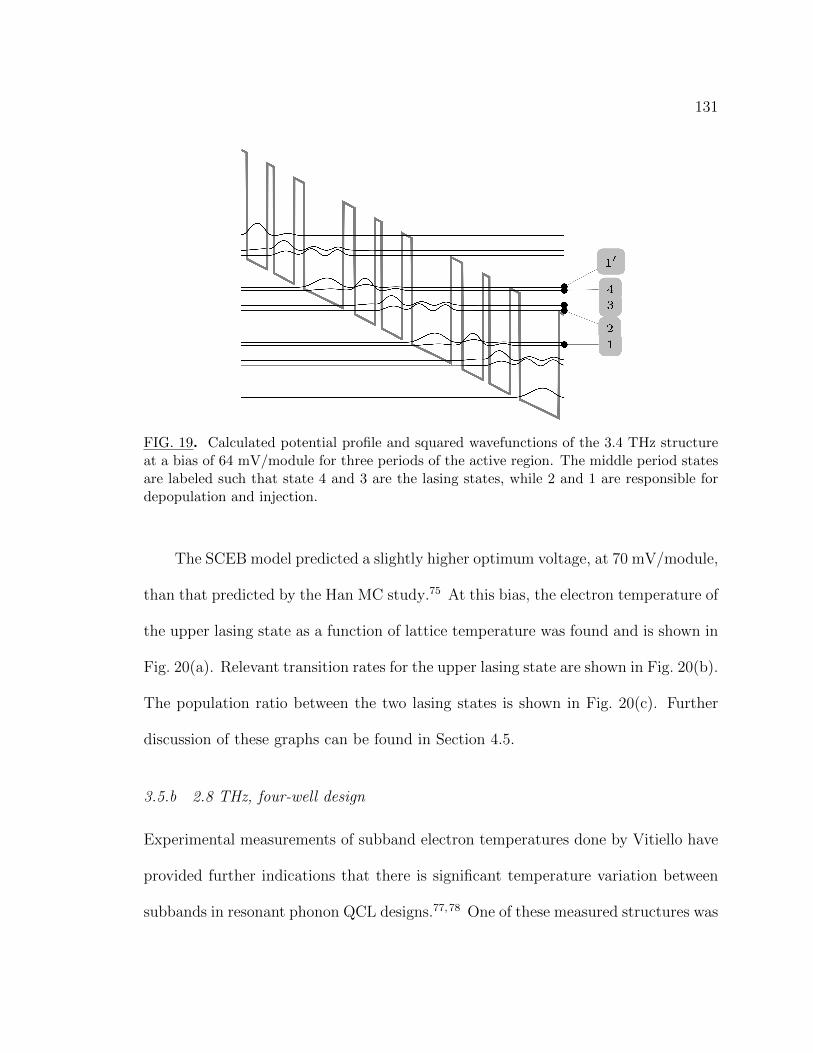
131
FIG. 19. Calculated potential profile and squared wavefunctions of the 3.4 THz structureat a bias of 64 mV/module for three periods of the active region. The middle period statesare labeled such that state 4 and 3 are the lasing states, while 2 and 1 are responsible fordepopulation and injection.
The SCEB model predicted a slightly higher optimum voltage, at 70 mV/module,
than that predicted by the Han MC study.75 At this bias, the electron temperature of
the upper lasing state as a function of lattice temperature was found and is shown in
Fig. 20(a). Relevant transition rates for the upper lasing state are shown in Fig. 20(b).
The population ratio between the two lasing states is shown in Fig. 20(c). Further
discussion of these graphs can be found in Section 4.5.
3.5.b 2.8 THz, four-well design
Experimental measurements of subband electron temperatures done by Vitiello have
provided further indications that there is significant temperature variation between
subbands in resonant phonon QCL designs.77,78 One of these measured structures was
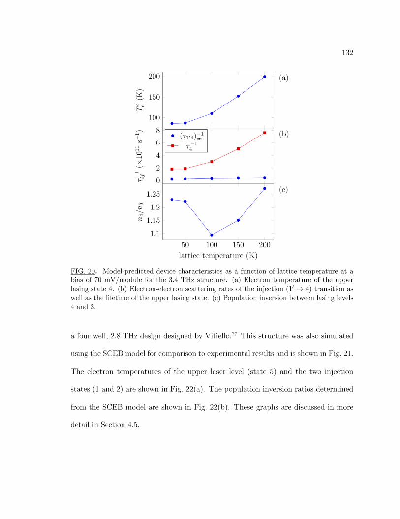
132
FIG. 20. Model-predicted device characteristics as a function of lattice temperature at abias of 70 mV/module for the 3.4 THz structure. (a) Electron temperature of the upperlasing state 4. (b) Electron-electron scattering rates of the injection (1′ → 4) transition aswell as the lifetime of the upper lasing state. (c) Population inversion between lasing levels4 and 3.
a four well, 2.8 THz design designed by Vitiello.77 This structure was also simulated
using the SCEB model for comparison to experimental results and is shown in Fig. 21.
The electron temperatures of the upper laser level (state 5) and the two injection
states (1 and 2) are shown in Fig. 22(a). The population inversion ratios determined
from the SCEB model are shown in Fig. 22(b). These graphs are discussed in more
detail in Section 4.5.
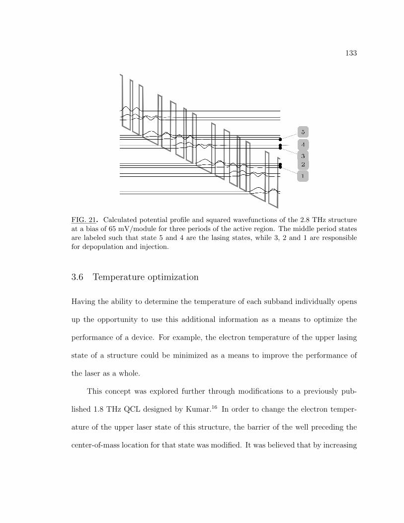
133
FIG. 21. Calculated potential profile and squared wavefunctions of the 2.8 THz structureat a bias of 65 mV/module for three periods of the active region. The middle period statesare labeled such that state 5 and 4 are the lasing states, while 3, 2 and 1 are responsiblefor depopulation and injection.
3.6 Temperature optimization
Having the ability to determine the temperature of each subband individually opens
up the opportunity to use this additional information as a means to optimize the
performance of a device. For example, the electron temperature of the upper lasing
state of a structure could be minimized as a means to improve the performance of
the laser as a whole.
This concept was explored further through modifications to a previously pub-
lished 1.8 THz QCL designed by Kumar.16 In order to change the electron temper-
ature of the upper laser state of this structure, the barrier of the well preceding the
center-of-mass location for that state was modified. It was believed that by increasing
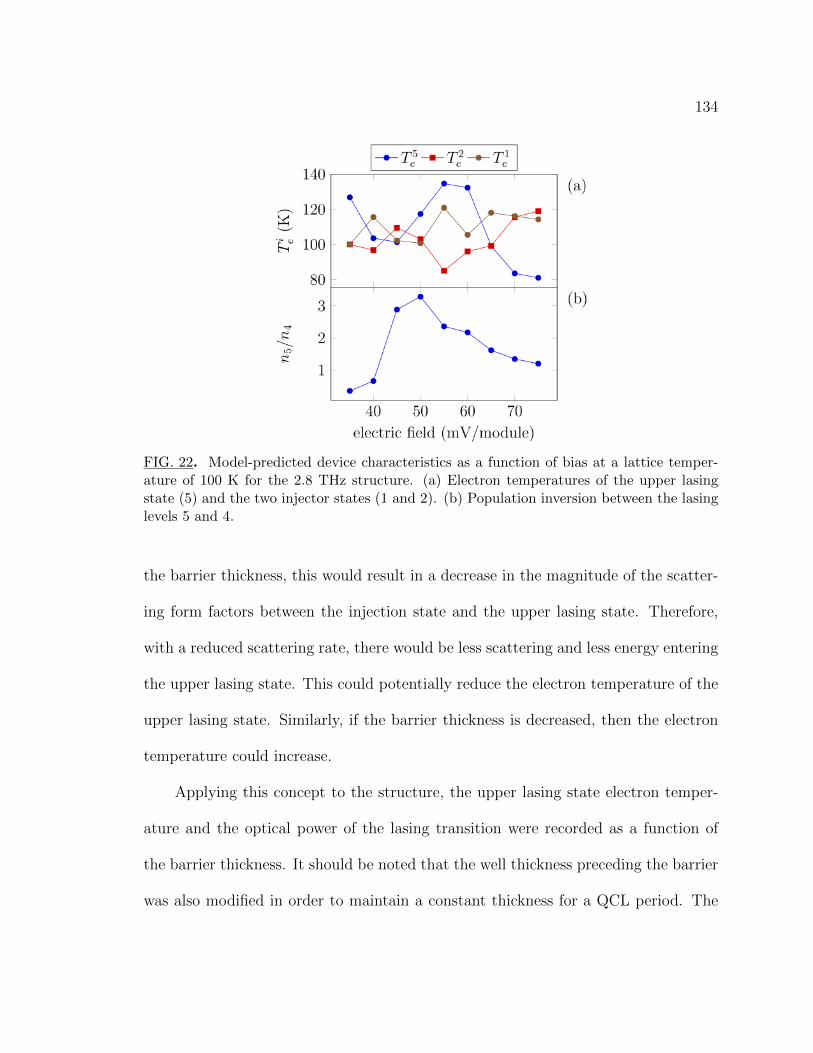
134
FIG. 22. Model-predicted device characteristics as a function of bias at a lattice temper-ature of 100 K for the 2.8 THz structure. (a) Electron temperatures of the upper lasingstate (5) and the two injector states (1 and 2). (b) Population inversion between the lasinglevels 5 and 4.
the barrier thickness, this would result in a decrease in the magnitude of the scatter-
ing form factors between the injection state and the upper lasing state. Therefore,
with a reduced scattering rate, there would be less scattering and less energy entering
the upper lasing state. This could potentially reduce the electron temperature of the
upper lasing state. Similarly, if the barrier thickness is decreased, then the electron
temperature could increase.
Applying this concept to the structure, the upper lasing state electron temper-
ature and the optical power of the lasing transition were recorded as a function of
the barrier thickness. It should be noted that the well thickness preceding the barrier
was also modified in order to maintain a constant thickness for a QCL period. The
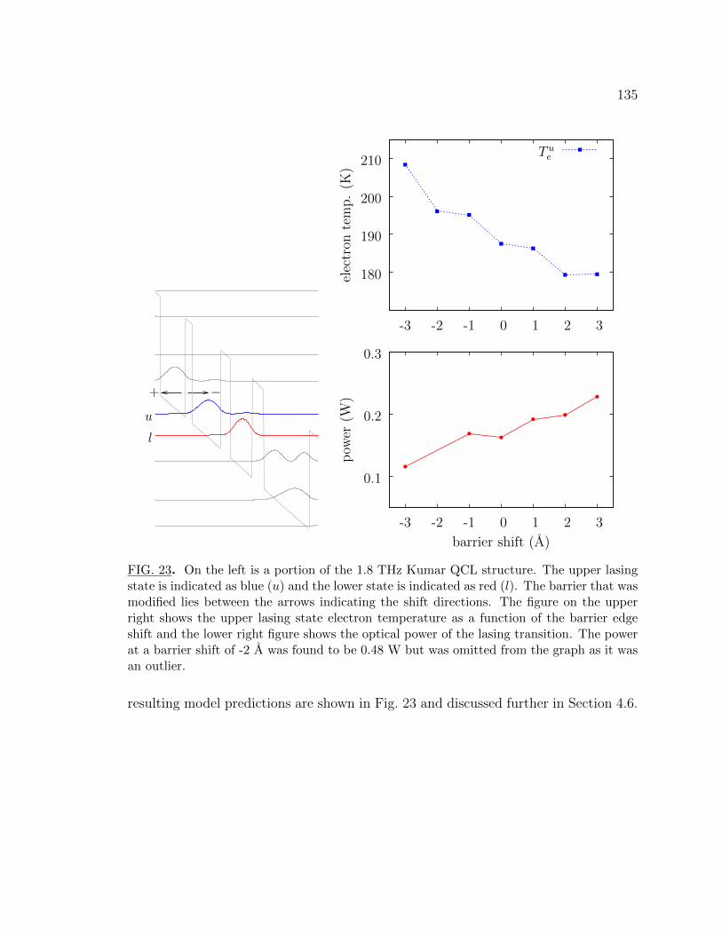
135
+ −
u
l
180
190
200
210
-3 -2 -1 0 1 2 3
elec
tron
tem
p.
(K)
0.1
0.2
0.3
-3 -2 -1 0 1 2 3
pow
er(W
)
barrier shift (A)
T ue
FIG. 23. On the left is a portion of the 1.8 THz Kumar QCL structure. The upper lasingstate is indicated as blue (u) and the lower state is indicated as red (l). The barrier that wasmodified lies between the arrows indicating the shift directions. The figure on the upperright shows the upper lasing state electron temperature as a function of the barrier edgeshift and the lower right figure shows the optical power of the lasing transition. The powerat a barrier shift of -2 A was found to be 0.48 W but was omitted from the graph as it wasan outlier.
resulting model predictions are shown in Fig. 23 and discussed further in Section 4.6.
136
IV. DISCUSSIONS
4.1 Average Electron Temperature
A study of the average electron temperature as a function of the electron states was
described in Section 3.1. The results of that study are shown in Table 4, which shows
a considerable amount of variation among the calculated electron temperatures. This
was expected since, as mentioned in Section 3.1, the average electron temperature
would be weighted differently depending on which states comprise the additional 1/2
period. It should also be noted that all of the Te’s are lower than those calculated
by Harrison.67 This is most likely due to the fact that only symmetric electron-
electron scattering rates were used in this study. However, from these results, it
was concluded that any arbitrary choice of states in the computation will not lead
to the same temperature. A further study of this issue was performed in order to
determine if there is a set of states which produced a minimum deviation among
electron temperature calculations (see Section 3.1).
This optimal choice of states was found by studying the deviation among com-
binations of electron states of various sizes (i.e. consecutive groupings of 15, 16, 17,
. . . electron states). It was anticipated that the deviation would consistently decrease
as more states were included. Surprisingly, there is a clear minimum in standard
deviation when 20 states are used to calculate Te as seen in Fig. 5. This equates
to approximately 3/4 of the total number of states in three periods of the Sirtori
137
structure.87
Other QCL structures were modeled in order to examine the effect of different
electron state combinations on the calculated Te and the amount of deviation ob-
served. Structures designed by Barbieri90 and Page92 were used. Above threshold,
the Page structure exhibited very similar behavior to that of Sirtori’s structure. A
minimum in standard deviation was observed when 18 of the 24 electron states in
three periods were used to calculate Te (see Fig. 6). This corresponds to exactly 3/4
of the total number of states.
The Barbieri structure exhibited similar behavior with regards to which fraction
of electron states provides the lowest amount of deviation among the possible combi-
nations of consecutive states. However, in some cases the deviation was lowest at a
fraction higher than 3/4 of the total number of electron states. It should also be noted
that the mean Te’s that were calculated for the Barbieri structure were lower than
the TL used in the computational model, and so may have had some inaccuracies.
Comparisons between modeling results of the Page structure92 and experimen-
tal measurements by Spagnolo80 of the same device were made. First, devices were
modeled using below-threshold voltages, since these voltages were used in the ex-
perimental measurements. The calculated electron temperatures were smaller than
then the measured values. However, it should be noted that in Spagnolo’s paper,80
an offset value was applied to the measured Te’s to take into account heating by a
probe laser. Taking this offset value into account might have improved the agreement
between the measured Te’s and those simulated using the computational model. Also
138
since the lasers were operating below threshold, the steady-state assumptions of the
SCEB model may not have been applicable.
Finally, the same structure was modeled over a range of bias voltages, some
of which were at or above the threshold condition. These can be found in Fig. 7,
which shows the electron temperature results over a range of bias voltages and lattice
temperatures. In this figure, Te increases linearly with increasing TL. Also, the
calculated Te’s reached higher values compared to the Te’s calculated using below-
threshold conditions.
4.2 The effect of approximations on e-e scattering rates
Three structures (an infinite quantum well, the 2.9 THz Barbieri QCL,90 and the 3.9
THz Kumar QCL27) were studied to determine the effect of various e-e scattering rate
approximations on the calculated rates. First, the relative and non-relative wavevec-
tor definitions of the scattering rate in Eq. (118) were each calculated as a function
of the number of integration points. Then, the impact of including state-blocking
and screening was evaluated using several vital transitions within the structures. Fi-
nally, the importance of calculating transition rates other than the symmetric type
(i, i→ f, f) was examined.
4.2.a Convergence and integration types
The behavior of the integrals in Eq. (118) was studied as a function of the num-
ber of integration points to see whether the non-relative wavevector or the relative
139
wavevector form reached convergence with fewer points.
The scattering rate as a function of the number of integration points is shown in
Fig. 10 for the infinite quantum well at one particular temperature and population
density. The non-relative form seems to have converged before the relative form;
however, this was not always the case at different temperatures and populations.
The situation was equally complex in the modeled QCL structures making it difficult
to reach a conclusion as to the superiority of one form over another in terms of
convergence speed.
In order to make a general statement about the relative performance of the inte-
gration types, the percent error was averaged from each scattering rate at a particular
temperature. The average percent error created from computational modeling of the
Barbieri design is shown in Figs. 11(a) and 11(b) as a function of the number of
integration points. Despite the averaging, neither form consistently converged faster
than the other. This is also the case in the Kumar design as shown in Figs. 12(a) and
12(b). However, both Figs. 11 and 12 have lower percent error at higher numbers of
integration points and indicate that in order to guarantee a percent error of less than
1% at all temperatures, 108 points (or 100 points per integration axis) must be used.
4.2.b State-blocking and screening
The effects of both screening and state-blocking were studied using the three struc-
tures mentioned so far. For the infinite quantum well, the lowest two states were
once again used to find the scattering rate W1,1→0,0. As shown in Fig. 13, this rate
140
was studied as a function of 2D population density Ni as well as temperature T .
As more carriers were present in the well, a reduction of the scattering rates due to
screening and state-blocking became more noticeable, where screening had the most
pronounced impact with an increase in Ni.
The 2.9 THz Barbieri QCL90 was studied in a similar manner. Two transitions
were singled out to demonstrate the reduction in scattering rates due to these effects.
First, the primary transition responsible for depopulation was plotted as a function
of the initial and final population densities (Ni and Nf , respectively) as well as tem-
perature (Fig. 14). Due to the large number of states within each period of the active
region, screening had a noticeable impact and reduced the rates by 10 to 15 percent.
State-blocking reduced the rates by only 1 to 2 percent.
The 3.9 THz Kumar QCL27 was also studied. A vital injection transition was
examined in Fig. 15. Screening was once again significant, reducing the rates by 5 to
10 percent. State-blocking was only noticeable at higher carrier densities and only
reduced the rates by 1 to 2 percent.
4.2.c Symmetric and asymmetric transitions
Results were obtained to study the relative magnitude of symmetric and asymmetric
scattering rates. The scattering events which contributed to the upper-state injection
transition rate W11,10 in the Barbieri structure are listed in Table 5. The symmet-
ric scattering event 11, 11 → 10, 10 is seen to have only the fifth highest rate of
the scattering events included. Scattering events of the type 11,m → 10,m and
141
m, 11→ m, 10, where m is one of the four adjacent subbands, are seen to contribute
significantly to the transition rate W11,10. When all possible scattering events among
the four adjacent subbands are summed, a total transition rate of 4.51× 10¹⁰ (1/s) is
found. This is eight times greater than the transition rate found from just symmetric
scattering events. Therefore, it is essential that scattering events of this type along
with the symmetric one be considered when determining transition rates which will
eventually be used in the rate equations.
Similar results were observed with the RP structure as shown in Table 6, where
the symmetric transition rate (4, 4→ 3, 3) is only the fifth highest rate among those
listed. This transition is also responsible for injection into the upper lasing state
(subband 3). When all possible scattering events are summed, a total transition rate
of 6.97×10¹⁰ (1/s) is found. This is eleven times greater than the symmetric transition
rate and is verified by comparison to Han’s Monte Carlo simulations.75 Once again,
the influence of these additional scattering events must be considered to improve the
accuracy of transition rates.
4.3 Scaling Studies
The scaling studies shown in Figs. 16 and 17 from Section 3.3 indicate the ability of
the QCL computational model to be used as an accurate predictive tool. Not only
was the computational model able to predict a lasing frequency over a broad range of
scaling factors, but the agreement was very good between the predicted and measured
frequencies as well. The RMS value between the modeled and measured data was
142
0.0229 for the Freeman 1.9 THz QCL and 0.0858 for the Vitiello 2.83 THz QCL. This
indicates the potential use of the model to optimize device performance based on other
parameter studies. These results also indicate that, in general, uniformly increasing
the width of a QCL structure a small fraction will lower its lasing frequency without
necessarily destroying the lasing action. Note that the relationship between lasing
frequency and scale factor is non-linear, justifying the complex modeling approach
used in this work.
4.4 Screening Studies
During the course of the device scaling study explained in Section 3.3, the effect of
screening was also analyzed. In Fig. 18 from Section 3.4, the output power as a
function of both scaling factor and bias voltage is shown. The top portion of Fig. 18
shows the power with screening included in the e-e scattering rate calculations and
the bottom portion shows the power when screening is not included.
As discussed in Section 4.2, screening tends to reduce the magnitude of the
electron-electron scattering rates. This appears to lead to a reduction in output
power as seen by the difference in maximum voltages in both figures. Interestingly,
screening does not seem to significantly change the overall power vs. frequency vs. bias
behavior of the QCL beyond uniformly lowering the power.
Additionally, the effect of scaling on the relationship between bias voltage and
power can also be seen. With both screening on and off, a scaling factor which reduces
the size of the device leads to the need for a higher bias voltage to reach optimum
143
power output.
4.5 Multi-subband electron temperature model
The results of applying the multi-subband SCEB model to two QCL structures were
presented in Section 3.5 to illustrate the success of the model in matching other
studies of the same structures.
4.5.a 3.4 THz, three-well design
For this structure, the SCEB model predicted a slightly higher optimum voltage, at 70
mV/module, than that predicted by the MC study of Han.75 At this bias, the electron
temperature of the upper lasing state as a function of lattice temperature was found
and is shown in Fig. 20(a). At lower lattice temperatures, the electron temperature of
the upper lasing state (T 4e ) was significantly higher than TL. But as TL was increased
to 150 K and above, T 4e and TL were roughly equal. This behavior was also seen in the
MC study of this structure by Han,75 but T 4e was several degrees higher than in the
present study. This reduction in temperature was most likely due to a smaller overall
injection rate into the upper lasing state via electron-electron scattering as seen in
Fig. 20(b). Additionally, the predicted lifetime of the upper laser state was much lower
at higher TL due to increased electron-phonon emission. These discrepancies between
the SCEB and MC calculations indicated that the observed differences in electron
temperatures for this structure were most likely due to differences in the calculation
of scattering rates and screening. The reduced population inversion between the two
144
lasing states predicted by the SCEB model and shown in Fig. 20(c) can be explained
using the same arguments.
4.5.b 2.8 THz, four-well design
This structure was also modeled using the SCEB for comparison to experimental
results and is shown in Fig.21. The electron temperatures of the upper laser level
(state 5) and the two injection states (1 and 2) are shown in Fig. 22(a). At 60
mV/module, the SCEB model predicted a temperature difference between the upper
laser state and the two injector states of 25-38%. This is not as large as the almost
100% difference seen experimentally; however, MC simulations have never predicted
temperature variations of that magnitude in resonant phonon QCL designs. The
SCEB temperature variations are very close to that of MC simulations performed by
Callebaut of a similar device,39 which predicted subband temperature variations of
up to 38%. The subband temperatures reported in the MC study were 96, 111, and
102 K for the upper lasing, upper injector, and lower injector state, respectively. The
subband temperatures from the SCEB model were 99, 118, and 99 K for the same
states, which is in good agreement.
The population inversion ratios determined from the SCEB model are shown in
Fig. 22(b) and are nearly identical to the values measured by Vitiello.77 However, the
MC study of Callebaut of the similar structure39 yielded a population inversion ratio of
8 at the alignment voltage, which is considerably higher than that from measurement
or the present SCEB modeling. This higher population density of the upper laser
145
state is most likely due to the higher lifetime of 3.5 ps reported in that study as
compared to the 1.2 ps predicted by the SCEB model. However, the lifetime of the
lower lasing states predicted by the MC study and the present one were identical.
4.6 Temperature optimization
As described in Section 3.6, the barrier thickness of a THz QCL design was modified in
order to observe its effect on the upper lasing state electron temperature and optical
power. As shown in Fig. 23, as the barrier thickness was increased the electron
temperature decreased and the optical power increased. Conversely, a decrease in
barrier thickness resulted in an increase in electron temperature and a decrease in
power.
The observed relationship between optical power and upper state electron tem-
perature could be explained through two effects. First, if the temperature of the upper
lasing state is kept low, that should inhibit the parasitic transition where the upper
lasing state emits a phonon rather than a photon. Additionally, a lower temperature
would prevent electrons in the upper state from escaping quantum confinement and
entering the energy continuum above the conduction band minimum. If both of these
effects are reduced, then the population inversion should increase, which improves
the optical power for the lasing transition.
146
V. CONCLUSIONS
5.1 Average Electron Temperature Calculations
When more than 3/2 periods of a QCL active region are used in the computational
model, different combinations of 15 electron states produced different calculated val-
ues for the average electron temperature (Te). For the case of resonant phonon, mid-IR
designs in the above-threshold condition, the number of electron states which pro-
duced the least amount of variation among calculations of the electron temperature
was found to be 3/4 of the total number of states in a three-period model.
5.2 Electron-electron scattering rate approximations
The convergence of both the non-relative and relative wavevector forms of the scat-
tering rates from Eq. (118) were shown to improve with an increase in the number
of integration points. From this, it was concluded that if an error of less than 1
percent is needed, then 108 integration points (or 100 points per integration axis) are
necessary to calculate a scattering rate. Both forms were shown to lead to near iden-
tical results, so that the choice of which form to use is irrelevant. Within the QCL
structures, the scattering rate was shown to be significantly affected by screening,
with scattering rates reduced by up thirty percent in the Barbieri structure and ten
percent in the Kumar structure. In both devices, state-blocking was shown to only
reduce scattering rates by one to two percent and can therefore typically be omitted
147
from calculations. Finally, the importance of including both symmetric and asymmet-
ric scattering events when finding a transition rate was demonstrated. Asymmetric
scattering events were shown to increase the transition rate by a factor of eight in
the 11, 11→ 10, 10 transition of the Barbieri structure and by factor of eleven in the
4, 4→ 3, 3 transition of the Kumar structure.
5.3 Device scaling
The success of the QCL computational model in predicting the lasing frequency of
devices was discussed in Section 4.3. There was excellent agreement between predicted
and measured frequencies over a range of device scaling factors and frequencies. This
indicates the high accuracy of the model when determining QCL frequencies.
5.4 Electron-electron screening
As discussed in Section 4.4, a screening model was successfully implemented to im-
prove the accuracy of electron-electron scattering rate calculations. This implemen-
tation also affected the predicted power output of modeled devices. Results from
studies of the effects of screening were shown as both a function of bias voltage and
and scaling factor. These indicated that screening tended to decrease the predicted
output power.
148
5.5 Multi-subband energy balance model
A self-consistent model containing a multi-subband energy balance condition was
presented. This model was used to generate subband electron temperatures as well
other output parameters for two resonant phonon QCL designs. Detailed compar-
isons between MC simulations, experimental measurements and the SCEB model
were performed. The SCEB model predicted similar electron temperatures to those
of MC studies. The discrepancies observed in population densities were most likely
due to differences in scattering rate calculations. When applied to a structure mea-
sured experimentally, the SCEB model predicted the upper lasing state to have the
highest subband temperature within the device, which was verified experimentally.
Although the degree of subband temperature variation was not as high as that seen
in experiment, the population inversion did match. These results demonstrate that
the multi-subband energy balance model is an accurate and powerful tool for un-
derstanding electron subband dynamics, as well as for numerically optimizing QCL
designs.
5.6 Temperature optimization
A preliminary study was discussed in Section 4.6 to determine if the electron temper-
ature of the upper lasing state could be controlled through the manipulation of other
device parameters. In this study, the well thickness of a device design was modified
to both increase and decrease the upper lasing state temperature. Additionally, this
149
modification also affected the predicted output power of the device. It was observed
that as the upper lasing state temperature decreased, the output power increased.
150
VI. RECOMMENDATIONS
Future versions of the QCL computational model will include the effects of
electron-impurity and interface roughness scattering, which have been shown to be
significant in some THz QCL studies.43–47 Also, additional approximations that may
contribute to electron-electron scattering rate calculations should be examined fur-
ther, such as the impact of the exchange interaction.55–57
With regards to the energy balance equations, some improvements have been
suggested to the author which may have an impact on the the calculated electron
temperatures. Specifically, there are multiple ways in which the energy transition
rate can be determined, each of which may influence temperature calculations. The
effects of these various forms on the electron temperatures as well as the predicted
QCL output properties should be studied further.
Once the energy balance equations have been fully integrated into the QCL com-
putational code, the electron temperatures could be used as an optimization tool, as
briefly discussed in Section 4.6. As far as the author is aware, this optimization
parameter has never been pursued in the literature, and may provide insight into
increasing high temperature performance of THz QCL’s. Additionally, electron tem-
perature could be used as a figure of merit in an automated optimization process.
For example, a genetic algorithm could be applied to a QCL design using the upper
lasing state temperature as part of a fitness function. Such a procedure could yield
new and practical designs.
151
VII. REFERENCES
[1] P. Siegel, “Terahertz technology,” Microwave Theory and Techniques, IEEETransactions on, vol. 50, pp. 910 – 928, 2002.
[2] W. L. Chan, J. Deibel, and D. M. Mittleman, “Imaging with terahertz radiation,”Reports on Progress in Physics, vol. 70, p. 1325, 2007.
[3] P. Siegel, “Terahertz technology in biology and medicine,” Microwave Theoryand Techniques, IEEE Transactions on, vol. 52, pp. 2438 – 2447, 2004.
[4] H.-T. Chen, R. Kersting, and G. C. Cho, “Terahertz imaging with nanometerresolution,” Applied Physics Letters, vol. 83, pp. 3009 – 3011, 2003.
[5] P. Y. Han, G. C. Cho, and X.-C. Zhang, “Time-domain transillumination ofbiological tissues with terahertz pulses,” Optics Letters, vol. 25, pp. 242 – 244,2000.
[6] K. Humphreys, J. Loughran, M. Gradziel, W. Lanigan, T. Ward, J. Murphy, andC. O’Sullivan, “Medical applications of terahertz imaging: a review of currenttechnology and potential applications in biomedical engineering,” in Engineeringin Medicine and Biology Society, 2004. IEMBS ’04. 26th Annual InternationalConference of the IEEE, vol. 1, pp. 1302 – 1305, 2004.
[7] C. S. Joseph, A. N. Yaroslavsky, J. L. Lagraves, T. M. Goyette, and R. H.Giles, “Dual-frequency continuous-wave terahertz transmission imaging of non-melanoma skin cancers,” vol. 7601, p. 760104, SPIE, 2010.
[8] J. E. Bjarnason, T. L. J. Chan, A. W. M. Lee, M. A. Celis, and E. R. Brown,“Millimeter-wave, terahertz, and mid-infrared transmission through commonclothing,” Applied Physics Letters, vol. 85, pp. 519 – 521, 2004.
[9] J. C. Dickinson, T. M. Goyette, A. J. Gatesman, C. S. Joseph, Z. G. Root,R. H. Giles, J. Waldman, and W. E. Nixon, “Terahertz imaging of subjects withconcealed weapons,” vol. 6212, p. 62120Q, SPIE, 2006.
[10] B. B. Hu and M. C. Nuss, “Imaging with terahertz waves,” Optics Letters, vol. 20,pp. 1716 – 1718, 1995.
[11] D. Mittleman, M. Gupta, R. Neelamani, R. Baraniuk, J. Rudd, and M. Koch,“Recent advances in terahertz imaging,” Applied Physics B: Lasers and Optics,vol. 68, pp. 1085 – 1094, 1999.
152
[12] K. Kawase, Y. Ogawa, Y. Watanabe, and H. Inoue, “Non-destructive terahertzimaging of illicit drugs using spectral fingerprints,” Optics Express, vol. 11,pp. 2549 – 2554, 2003.
[13] E. J. Slingerland, M. K. Vallon, E. G. E. Jahngen, R. H. Giles, and T. M.Goyette, “Terahertz absorption spectra of highly energetic chemicals,” vol. 7671,p. 76710A, SPIE, 2010.
[14] A. Hirata, T. Kosugi, H. Takahashi, R. Yamaguchi, F. Nakajima, T. Furuta,H. Ito, H. Sugahara, Y. Sato, and T. Nagatsuma, “120-GHz-band millimeter-wave photonic wireless link for 10-Gb/s data transmission,” Microwave Theoryand Techniques, IEEE Transactions on, vol. 54, pp. 1937 – 1944, 2006.
[15] N. Krumbholz, K. Gerlach, F. Rutz, M. Koch, R. Piesiewicz, T. Kurner, andD. Mittleman, “Omnidirectional terahertz mirrors: A key element for futureterahertz communication systems,” Applied Physics Letters, vol. 88, p. 202905,2006.
[16] S. Kumar, C. W. I. Chan, Q. Hu, and J. L. Reno, “A 1.8-THz quantum cascadelaser operating significantly above the temperature of ~ω/kB,” Nature Physics,vol. 7, pp. 166 – 171, 2011.
[17] B. S. Williams, “Terahertz quantum-cascade lasers,” Nature Photonics, vol. 1,pp. 517 – 525, 2007.
[18] D. Woolard, R. Brown, M. Pepper, and M. Kemp, “Terahertz frequency sensingand imaging: A time of reckoning future applications?,” Proceedings of the IEEE,vol. 93, pp. 1722 – 1743, 2005.
[19] I. Mehdi, G. Chattopadhyay, E. Schlecht, J. Ward, J. Gill, F. Maiwald, andA. Maestrini, “Terahertz multiplier circuits,” in Microwave Symposium Digest,2006. IEEE MTT-S International, pp. 341 – 344, 2006.
[20] A. Maestrini, J. Ward, J. Gill, H. Javadi, E. Schlecht, G. Chattopadhyay, F. Mai-wald, N. Erickson, and I. Mehdi, “A 1.7-1.9 THz local oscillator source,” Mi-crowave and Wireless Components Letters, IEEE, vol. 14, no. 6, no. 6, pp. 253– 255, 2004.
[21] M. Tonouchi, “Cutting-edge terahertz technology,” Nature Photonics, vol. 1,pp. 97 – 105, 2007.
[22] B. Ferguson and X.-C. Zhang, “Materials for terahertz science and technology,”Nature Materials, vol. 1, pp. 26 – 33, 2002.
153
[23] R. F. Kazarinov and R. A. Suris, “Possibility of the amplification of electromag-netic waves in a semiconductor with a superlattice,” Soviet Physics - Semicon-ductors, vol. 5, pp. 707 – 709, 1971.
[24] J. Faist, F. Capasso, D. L. Sivco, C. Sirtori, A. L. Hutchinson, and A. Y. Cho,“Quantum cascade laser,” Science, vol. 264, pp. 553 – 556, 1994.
[25] R. Kohler, A. Tredicucci, F. Beltram, H. E. Beere, E. H. Linfield, A. G.Davies, D. A. Ritchie, R. C. Iotti, and F. Rossi, “Terahertz semiconductor-heterostructure laser,” Nature, vol. 417, pp. 156 – 159, 2002.
[26] B. S. Williams, S. Kumar, Q. Hu, and J. L. Reno, “High-power terahertzquantum-cascade lasers,” Electronics Letters, vol. 42, pp. 89 – 91, 2006.
[27] S. Kumar, Q. Hu, and J. L. Reno, “186 K operation of terahertz quantum-cascaded lasers based on a diagonal design,” Applied Physics Letters, vol. 94,p. 131105, 2009.
[28] C. Walther, M. Fischer, G. Scalari, R. Terazzi, N. Hoyler, and J. Faist, “Quantumcascade lasers operating from 1.2 to 1.6 THz,” Applied Physics Letters, vol. 91,p. 131122, 2007.
[29] P. Harrison and R. Kelsall, “The relative importance of electron-electron andelectron-phonon scattering in terahertz quantum cascade lasers,” Solid-StateElectronics, vol. 42, pp. 1449 – 1451, 1998.
[30] D. Indjin, Z. Ikonic, V. D. Jovanovic, N. Vukmirovic, P. Harrison, and R. W. Kel-sall, “Relationship between carrier dynamics and temperature in terahertz quan-tum cascade structures: simulation of GaAs/AlGaAs, SiGe/Si and GaN/AlGaNdevices,” Semiconductor Science and Technology, vol. 20, pp. S237 – S245, 2005.
[31] R. C. Iotti and F. Rossi, “Carrier thermalization versus phonon-assisted relax-ation in quantum-cascade lasers: A Monte Carlo approach,” Applied PhysicsLetters, vol. 78, p. 2902, 2001.
[32] X. Gao, D. Botez, and I. Knezevic, “χ-valley leakage in GaAs-based midinfraredquantum cascade lasers: A Monte Carlo study,” Journal of Applied Physics,vol. 101, p. 063101, 2007.
[33] S. M. Goodnick and P. Lugli, “Effect of electron-electron scattering on nonequi-librium transport in quantum-well systems,” Physical Review B, vol. 37, pp. 2578– 2588, 1988.
154
[34] S.-C. Lee and A. Wacker, “Nonequilibrium greens function theory for transportand gain properties of quantum cascade structures,” Physical Review B, vol. 66,p. 245314, 2002.
[35] R. Lake, G. Klimeck, R. C. Bowen, and D. Jovanovic, “Single and multibandmodeling of quantum electron transport through layered semiconductor devices,”Journal of Applied Physics, vol. 81, pp. 7845 – 7869, 1997.
[36] T. Schmielau and J. M. F. Pereira, “Nonequilibrium many body theory for quan-tum transport in terahertz quantum cascade lasers,” Applied Physics Letters,vol. 95, no. 23, no. 23, p. 231111, 2009.
[37] T. Kubis, C. Yeh, P. Vogl, A. Benz, G. Fasching, and C. Deutsch, “Theory ofnonequilibrium quantum transport and energy dissipation in terahertz quantumcascade lasers,” Physical Review B, vol. 79, p. 195323, 2009.
[38] H. Yasuda, T. Kubis, P. Vogl, N. Sekine, I. Hosako, and K. Hirakawa, “Nonequi-librium green’s function calculation for four-level scheme terahertz quantum cas-cade lasers,” Applied Physics Letters, vol. 94, p. 151109, 2009.
[39] H. Callebaut, S. Kumar, B. S. Williams, Q. Hu, and J. L. Reno, “Analysisof transport properties of terahertz quantum cascade lasers,” Applied PhysicsLetters, vol. 83, p. 207, 2003.
[40] S. Kumar and Q. Hu, “Coherence of resonant-tunneling transport in terahertzquantum-cascade lasers,” Physical Review B, vol. 80, p. 245316, 2009.
[41] G. Beji, Z. Ikonic, C. A. Evans, D. Indjin, and P. Harrison, “Coherent transportdescription of the dual-wavelength ambipolar terahertz quantum cascade laser,”Journal of Applied Physics, vol. 109, p. 013111, 2011.
[42] V. D. Jovanovic, S. Hufling, D. Indjin, N. Vukmirovic, Z. I. P. Harrison,J. P. Reithmaier, and A. Forchel, “Influence of doping on electron dynamicsin GaAs/AlGaAs quantum cascade lasers,” Journal of Applied Physics, vol. 99,p. 103106, 2006.
[43] K. Hess, “Impurity and phonon scattering in layered structures,” Applied PhysicsLetters, vol. 35, pp. 484–486, 1979.
[44] H. Callebaut, S. Kumar, B. S. Williams, Q. Hu, and J. L. Reno, “Importance ofelectron-impurity scattering for electron transport in terahertz quantum-cascadelasers,” Applied Physics Letters, vol. 84, p. 645, 2004.
155
[45] R. Nelander and A. Wacker, “Temperature dependence and screening models inquantum cascade structures,” Journal of Applied Physics, vol. 106, p. 063115,2009.
[46] S. Tsujino, A. Borak, E. Muller, M. Scheinert, C. V. Falub, H. Sigg, D. Grutz-macher, M. Giovannini, and J. Faist, “Interface-roughness-induced broadeningof intersubband electroluminescence in p-SiGe and n-GaInAs/AlInAs quantum-cascade structures,” Applied Physics Letters, vol. 86, p. 062113, 2005.
[47] T. Kubis and G. Klimeck, “Rough interfaces in THz quantum cascade lasers,” inComputational Electronics (IWCE), 2010 14th International Workshop on, pp. 1– 4, 2010.
[48] C. G. Van de Walle, “Band lineups and deformation potentials in the model-solidtheory,” Physical Review B, vol. 39, pp. 1871 – 1883, 1989.
[49] I. Vurgaftman, J. R. Meyer, and L. R. Ram-Mohan, “Band parameters for III–Vcompound semiconductors and their alloys,” Journal of Applied Physics, vol. 89,pp. 5815 – 5875, 2001.
[50] P. Kinsler, P. Harrison, and R. W. Kelsall, “Intersubband terahertz lasers usingfour-level asymmetric quantum wells,” Journal of Applied Physics, vol. 85, pp. 23– 28, 1999.
[51] S.-C. Lee and I. Galbraith, “Multisubband nonequilibrium electron-electron scat-tering in semiconductor quantum wells,” Physical Review B, vol. 55, pp. R16025– R16028, 1997.
[52] B. S. Williams, Terahertz quantum cascade lasers. PhD thesis, MassachusettsInstitute of Technology, 2003.
[53] J. H. Smet, C. G. Fonstad, and Q. Hu, “Intrawell and interwell intersubbandtransitions in multiple quantum wells for far-infrared sources,” Journal of AppliedPhysics, vol. 79, pp. 9305 – 9320, 1996.
[54] P. Harrison, Quantum Wells, Wires and Dots. Hoboken, New Jersey: Wiley,second ed., 2005.
[55] A. Moskova and M. Mosko, “Exchange carrier-carrier scattering of photo-excitedspin-polarized in GaAs quantum wells: Monte Carlo study,” Physical Review B,vol. 49, pp. 7443 – 7452, 1994.
[56] M. Mosko, A. Moskova, and V. Cambel, “Carrier-carrier scattering in photoex-cited intrinsic GaAs quantum wells and its effect on femtosecond plasma ther-malization,” Physical Review B, vol. 51, pp. 16860 – 16866, 1995.
156
[57] S.-C. Lee and I. Galbraith, “Influence of exchange scattering and dynamic screen-ing on electron-electron scattering rates in semiconductor quantum wells,” Phys-ical Review B, vol. 62, pp. 15327 – 15330, 2000.
[58] S. M. Goodnick and P. Lugli, “Subpicosecond dynamics of electron injection intoGaAs/AlGaAs quantum wells,” Applied Physics Letters, vol. 51, p. 584, 1987.
[59] H. Haug and S. W. Koch, Quantum Theory of the Optical and ElectronicPropeties of Semiconductors. New Jersey: World Scientific, fourth ed., 2004.
[60] P. F. Maldague, “Many-body corrections to the polarizability of the two-dimensional electron gas,” Surface Science, vol. 73, pp. 296 – 302, 1978.
[61] T. Ando, A. B. Fowler, and F. Stern, “Electronic properties of two-dimensionalsystems,” Reviews of Modern Physics, vol. 54, p. 437, 1982.
[62] K. Donovan, P. Harrison, and R. W. Kelsall, “Self-consistent solutions tothe intersubband rate equations in quantum cascade lasers: Analysis of aGaAs/AlxGa1−xAs device,” Journal of Applied Physics, vol. 89, pp. 3084 – 3090,2001.
[63] M. Troccoli, G. Scamarcio, V. Spagnolo, A. Tredicucci, C. Gmachl, F. Capasso,D. L. Sivco, A. Y. Cho, and M. Striccoli, “Electronic distribution in superlatticequantum cascade lasers,” Applied Physics Letters, vol. 77, pp. 1088 – 1090, 2000.
[64] D. Indjin, P. Harrison, R. W. Kelsall, and Z. Ikonic, “Mechanisms of temperatureperformance degradation in terahertz quantum-cascade lasers,” Applied PhysicsLetters, vol. 82, pp. 1347 – 1349, 2003.
[65] C. Jirauschek and P. Lugli, “Limiting factors for high temperature operation ofTHz quantum cascade lasers,” Physica Status Solidi (c), vol. 5, pp. 221 – 224,2008.
[66] L. Lever, A. Valavanis, C. A. Evans, Z. Ikonic, and R. W. Kelsall, “The impor-tance of electron temperature in silicon-based terahertz quantum cascade lasers,”Applied Physics Letters, vol. 95, p. 131103, 2009.
[67] P.Harrison, D. Indjin, and R. W. Kelsall, “Electron temperature and mechanismsof hot carrier generation in quantum cascade lasers,” Journal of Applied Physics,vol. 92, p. 6921, 2002.
[68] D. Indjin, P. Harrison, R. Kelsall, and Z. Ikonic, “Self-consistent scattering modelof carrier dynamics in GaAs/AlGaAs terahertz quantum-cascade lasers,” Pho-tonics Technology Letters, IEEE, vol. 15, pp. 15 – 17, 2003.
157
[69] J. M. Tavish, D. Indjin, and P. Harrison, “Aspects of the internal physics ofInGaAs/InAlAs quantum cascade lasers,” Journal of Applied Physics, vol. 99,p. 114505, 2006.
[70] P. Harrison, D. Indjin, V. D. Jovanovic, A. Mircetic, Z. Ikonic, R. W. Kelsall,J. McTavish, I. Savic, N. Vukmirovic, and V. Milanovic, “A physical model ofquantum cascade lasers: Application to GaAs, GaN and SiGe devices,” PhysicaStatus Solidi (a), vol. 202, pp. 980 – 986, 2005.
[71] H. Callebaut and Q. Hu, “Importance of coherence for electron transport interahertz quantum cascade lasers,” Journal of Applied Physics, vol. 98, p. 104505,2005.
[72] O. Bonno, J.-L. Thobel, and F. Dessenne, “2.9 THz quantum cascade lasersoperating up to 70 K in continuous wave,” Journal of Applied Physics, vol. 97,p. 043702, 2005.
[73] J. T. Lu and J. C. Cao, “Coulomb scattering in the Monte Carlo simulation ofterahertz quantum-cascade lasers,” Applied Physics Letters, vol. 89, p. 211115,2006.
[74] C. Jirauschek, A. Matyas, and P. Lugli, “Modeling bound-to-continuum terahertzquantum cascade lasers: The role of Coulomb interactions,” Journal of AppliedPhysics, vol. 107, p. 013104, 2010.
[75] Y. J. Han and J. C. Cao, “Monte Carlo simulation of carrier dynamics in tera-hertz quantum cascade lasers,” Journal of Applied Physics, vol. 108, p. 093111,2010.
[76] R. C. Iotti, F. Rossi, M. S. Vitiello, G. Scamarcio, L. Mahler, and A. Tredicucci,“Impact of nonequilibrium phonons on the electron dynamics in terahertz quan-tum cascade lasers,” Applied Physics Letters, vol. 97, p. 033110, 2010.
[77] M. S. Vitiello, G. Scamarcio, V. Spagnolo, B. S. Williams, S. Kumar, Q. Hu,and J. L. Reno, “Measurement of subband electronic temperatures and popula-tion inversion in THz quantum-cascade lasers,” Applied Physics Letters, vol. 86,p. 111115, 2005.
[78] M. S. Vitiello, G. Scamarcio, V. Spagnolo, C. Worrall, H. E. Beere, D. A. Ritchie,C. Sirtori, J. Alton, and S. Barbieri, “Subband electronic temperatures andelectron-lattice energy relaxation in terahertz quantum cascade lasers with dif-ferent conduction band offsets,” Applied Physics Letters, vol. 89, p. 131114, 2006.
158
[79] Z. Ikonic, P. Harrison, and R. W. Kelsall, “Self-consistent energy balance simu-lations of hole dynamics in SiGe/Si THz quantum cascade structures,” Journalof Applied Physics, vol. 96, p. 6803, 2004.
[80] V. Spagnolo, G. Scamarcio, H. Page, and C. Sirtori, “Simultaneous measure-ment of the electronic and lattice temperatures in GaAs/Al0.45Ga0.55As quantum-cascade lasers: Influence on the optical performance,” Applied Physics Letters,vol. 84, pp. 3690 – 3692, 2004.
[81] R. Terazzi and J. Faist, “A density matrix model of transport and radiation inquantum cascade lasers,” New Journal of Physics, vol. 12, p. 033045, 2010.
[82] C. Baird, B. Crompton, P. Slingerland, R. Giles, and W. E. Nixon, “Optimiza-tion of semi-insulating surface-plasmon waveguides within terahertz QCL’s usingcomputational models,” Proc. SPIE, vol. 7671, p. 767109, 2010.
[83] R. Kohler, A. Tredicucci, F. Beltram, H. E. Beere, E. H. Linfield, A. G. Davies,D. A. Ritchie, S. S. Dhillon, and C. Sirtori, “High-performance continuous-waveoperation of superlattice terahertz quantum-cascade lasers,” Applied Physics Let-ters, vol. 82, pp. 1518 – 1520, 2003.
[84] K. Donovan, P. Harrison, and R. W. Kelsall, “Stark ladders as tunable far-infrared emitters,” Journal of Applied Physics, vol. 84, pp. 5175 – 5179, 1998.
[85] P. Kinsler, P. Harrison, and R. W. Kelsall, “Intersubband electron-electron scat-tering in asymmetric quantum wells designed for far-infrared emission,” PhysicalReview B, vol. 58, pp. 4771 – 4778, 1998.
[86] S.-C. Lee and I. Galbraith, “Intersubband and intrasubband electronic scatteringrates in semiconductor quantum wells,” Physical Review B, vol. 59, pp. 15796 –15805, 1999.
[87] C. Sirtori, P. Kruck, S. Barbieri, P. Collot, J. Nagle, M. Beck, J. Faist, andU. Oesterle, “GaAs/AlxGa1−xAs quantum cascade lasers,” Applied Physics Let-ters, vol. 73, pp. 3486–3488, 1998.
[88] M. S. Vitiello, G. Scamarcio, V. Spagnolo, S. S. Dhillon, and C. Sirtori, “Ter-ahertz quantum cascade lasers with large wall-plug efficiency,” Applied PhysicsLetters, vol. 90, p. 191115, 2007.
[89] A. Danylov, Frequency Stabilization, Tuning, and Spatial Mode Control of Ter-ahertz Quantum Cascade Lasers for Coherent Transceiver Applications. PhDthesis, University of Massachusetts Lowell, 2010.
159
[90] S. Barbieri, J. Alton, H. E. Beere, J. Fowler, E. H. Linfield, and D. A. Ritchie,“2.9 THz quantum cascade lasers operating up to 70 K in continuous wave,”Applied Physics Letters, vol. 85, pp. 1674 – 1676, 2004.
[91] J. R. Freeman, J. Madeo, A. Brewer, S. Dhillon, O. P. Marshall, N. Jukam,D. Oustinov, J. Tignon, H. E. Beere, and D. A. Ritchie, “Dual wavelength emis-sion from a terahertz quantum cascade laser,” Applied Physics Letters, vol. 96,p. 051120, 2010.
[92] H. Page, C. Becker, A. Robertson, G. Glastre, V. Ortiz, and C. Sirtori, “300 Koperation of a GaAs-based quantum-cascade laser at λ ≈ 9 µm,” Applied PhysicsLetters, vol. 78, pp. 3529–3531, 2001.
[93] N. W. Ashcroft and N. D. Mermin, Solid State Physics. U. S.: Brooks/Cole,1976.
[94] B. K. Ridley, Quantum Processes in Semiconductors. New York: Oxford SciencePublictions, fourth ed., 1999.
[95] F. T. Vasko and O. E. Raichev, Quantum Kinetic Theory and Applications:Electrons, Photons, Phonons. New York: Springer, 2005.
[96] M. Dressel and G. Gruner, Electrodynamics of Solids: Optical Properties of Elec-trons in Matter. New York: Cambridge University Press, 2002.
160
VIII. BIOGRAPHY
Philip Slingerland graduated from Ithaca College in May 2004 with a Bachelor of
Arts degree in physics and a minor in mathematics. He then went to work for a civil
engineering consulting and testing company in Acton, Massachusetts for two years.
He then pursued his graduate education in physics at the University of Massachusetts
Lowell. His research focused on the optimization of terahertz quantum cascade lasers.
After acquiring his PhD, he will work as an analyst for Metron Scientific Solutions in
Reston, Virginia.