temperature-dependent thermal conductivity of … · temperature-dependent thermal conductivity of...
TRANSCRIPT

M. Asheghi
M. N. Touzelbaev
K. E. Goodson
[email protected] Mechanical Engineering Department,
Stanford University, Stanford, CA 94305-3030
Y. K. Leung
S. S. Wong
Electrical Engineering Department, Stanford University,
Stanford, CA 94305-3030
Temperature-Dependent Thermal Conductivity of Single-Crystal Silicon Layers in SOI Substrates Self heating diminishes the reliability of silicon-on-insulator (SOI) transistors, particularly those that must withstand electrostatic discharge (ESD) pulses. This problem is alleviated by lateral thermal conduction in the silicon device layer, whose thermal conductivity is not known. The present work develops a technique for measuring this property and provides data for layers in wafers fabricated using bond-and-etch-back (BESOI) technology. The room-temperature thermal conductivity data decrease with decreasing layer thickness, ds, to a value nearly 40 percent less than that of bulk silicon for ds = 0.42 \xm. The agreement of the data with the predictions of phonon transport analysis between 20 and 300 K strongly indicates that phonon scattering on layer boundaries is responsible for a large part of the reduction. The reduction is also due in part to concentrations of imperfections larger than those in bulk samples. The data show that the buried oxide in BESOI wafers has a thermal conductivity that is nearly equal to that of bulk fused quartz. The present work will lead to more accurate thermal simulations of SOI transistors and cantilever MEMS structures.
1 Introduction Silicon-on-insulator (SOI) circuits promise advantages in
speed and processing expense compared to circuits made from bulk silicon (e.g., Peters, 1993). The buried silicon-dioxide layer in SOI circuits has a very low thermal conductivity, which results in a large thermal resistance between the device and the chip packaging. This is a major problem for transistors that experience brief pulses of heating, such as ESD protection devices (e.g., Amerasekera et al , 1992), for which the temperature rise is dominated by conduction within micrometers of active regions. Lateral conduction parallel to the plane of the wafer in the silicon device layer can strongly reduce the temperature rise in active regions, such as the transistor channel (Good-son et al., 1995). However, this effect cannot be accurately predicted at present because the thermal conductivity of the device layer is not known. The lateral thermal conductivity of the silicon layer in SOI substrates is also important for the design of many MicroElectroMechanical Systems (MEMS) which use single-crystal silicon cantilevers that are etched from SOI substrates. One example is the cantilever of Chui et al. (1996), which uses heat pulses to make sub-micrometer pits in PMMA for high-density data storage.
Heat conduction in silicon is dominated by phonon transport, even in the presence of large concentrations of free charge carriers. The device-layer thermal conductivity is reduced compared to that of bulk silicon due to scattering mechanisms in the layer that are not present in the bulk material, such as those depicted in Fig. 1. Phonon-boundary scattering is particularly important at low temperatures, where the mean free path would otherwise become arbitrarily large. While phonon-boundary interactions govern the thermal conductivity of any silicon sample at low enough temperatures, the reduction is more severe and extends to higher temperatures for thin layers than for bulk samples. Also important is phonon scattering on imperfections, which exist in larger concentrations in SOI substrates than in
Contributed by the Heat Transfer Division for publication in the JOURNAL OF HEAT TRANSFER and presented at the 1996 ASME IMECE. Manuscript received by the Heat Transfer Division August 21, 1996; revision received September 23, 1997; Keywords: Conduction; Measurement Techniques; Thermophysical Properties. Associate Technical Editor: A. S. Lavine.
bulk material. The higher concentrations result from steps in the wafer fabrication process, such as SIMOX implantation (e.g., Cellar and White, 1992) and the epitaxial growth process of BESOI wafers (Maszara, 1991). While the impact of these imperfections on electrical transport has been studied, there has been little progress on modeling or measuring their impact on heat transport. Finally, the impurities and additional free carriers in doped semiconducting regions impede heat transport compared to that in bulk intrinsic silicon (Goodson and Cooper, 1995). There are data available for the thermal conductivity of bulk doped samples (Touloukian et al., 1970a) which show a strong reduction for impurity concentrations greater than about 5 X 1019 cm - 3 , but it is not clear if the bulk data are appropriate for layers doped using thin-film implantation and diffusion techniques.
Previous work (Paul et al., 1993, 1994; Von Arx and Baltes, 1992; Von Arx et al , 1995; Mastrangelo and Miiller, 1988; Tai et al., 1988) measured the lateral thermal conductivity of doped polysilicon layers. These authors reported a reduction of up to 80 percent compared to the conductivity of bulk intrinsic silicon. While it is not clear which of the mechanisms shown in Fig. 1 is responsible for the reduction in the polysilicon layers for which data are available, it is likely that the grain boundaries are responsible for a fraction of the reduction. It would therefore be inappropriate to assume that the thermal conductivity of the crystalline layers in SOI substrates can be determined using the existing data for poly crystalline samples.
Very few data are available for the thermal conductivity of single-crystal silicon samples with submillimeter dimensions. Savvides and Goldsmid (1973) measured the thermal conductivity of pure and neutron-irradiated crystalline silicon with dimensions comparable to 20, 40, 60, and 100 p,m at temperatures of 200 and 300 K. They did not observe a size effect on the thermal conductivity even for the thinnest pure silicon specimen at 200 K. Yu et al. (1996) measured the thermal diffusivity of a 4 fim thick, free-standing silicon film at room temperature and observed no significant reduction in the thermal diffusivity compared to that of bulk samples. However, a recent study reported a two orders of magnitude reduction in the thermal conductivity of a 0.15 //m thick silicon layer made using SIMOX technology at temperatures between 330 and 380 K
30 / Vol. 120, FEBRUARY 1998 Copyright © 1998 by ASME Transactions of the ASME
Downloaded 21 Nov 2008 to 171.64.49.29. Redistribution subject to ASME license or copyright; see http://www.asme.org/terms/Terms_Use.cfm

PHONON- PHONON- PHONON- PHONON-BOUNDARY IMPERFECTION IMPURITY ELECTRON SCATTERING SCATTERING SCATTERING SCATTERING
yfV IMPERFECTION PHONON
PHONON
IMPERFECTION PHONON PHONON
„..,,.,„., IMPURITY • PHONON A T n M „ c r T n n „
ds
Fig. 1 Phonon scattering mechanisms which reduce the thermal conductivity of SOI device layers compared to that of bulk intrinsic silicon. The thermal conductivity of silicon is dominated by phonon transport.
(Zheng et al , 1996). These data motivate the present study, which provides a systematic measurement of the thermal conductivities of single-crystal silicon layers of thickness comparable to and less than one micrometer. The resulting data are of practical relevance for SOI devices and are of fundamental interest because of the information they provide about phonon free paths in the bulk material.
This work develops a technique for measuring the lateral thermal conductivity of SOI device layers. The technique has the advantage that it uses doping and photolithography techniques that are compatible with CMOS technology, such that it can be directly integrated onto an SOI wafer for parallel device and thermal-property characterization. The measurements yield the vertical thermal resistance of the buried silicon dioxide as well as the lateral thermal conductivity of the silicon device layer using two separate structures. This manuscript reports data for BESOI silicon layers of thickness between 0.4 and 1.6 /jm at temperatures between 20 and 300 K. The range of thicknesses and temperatures aids with the determination of the relative importance of the phonon-boundary scattering mechanism. The data provided here assist with the study of self heating in thin-film SOI transistors. They are also important for the design of the large variety of microscopic thermal sensors and actuators that are made from SOI substrates. From a more fundamental viewpoint, study of the thermal conductivity in thin crystalline silicon films provides an opportunity to more directly determine the spectrum of phonon mean free paths in this material, by means of the conductivity reduction due to phonon boundary
scattering. The potential for such fundamental study is particularly large in SOI wafers, whose device layers resemble the bulk material in purity and microstructural quality.
2 Experimental Structures and Procedure Figure 2 shows a cross-sectional schematic and an electron
micrograph of the experimental structure used to measure the lateral thermal conductivity of the SOI device layer. The wafers in the present study are fabricated using BESOI technology, in which ap+ epitaxial layer doped with about 1020 boron atoms ever3 serves as the etch stop. The device layer is grown on the etch-stop layer and is doped with less than 1015 boron atoms cm"3 due to the residual boron in the chamber. After the bonding, the silicon substrate is etched with a KOH/isopropyl alcohol solution which stops at the p+ layer. The p+ layer is then removed using a 1:3:8 solution of 49 percent HF, 70 percent HN03 , and 98 percent CH3COOH. This solution selectively etches the p + region and stops at the undoped layer. The moderately doped bridge, which is used here as a heater for the thermal conductivity measurements, is fabricated using a 50 keV implantation of BF2+ with dosage 5 X 1015 cm"2 and a subsequent 30 minute anneal at 1220 K. Two sets of structures are used in the present study, distinguished by the die from which they are fabricated. Data reported here over the temperature range of 20 to 300 K are obtained from die no. 1 with silicon device layer thicknesses ds = 0.42, 0.83, and 1.6 p,m and buried oxide thickness d0 = 3 /xm. Data are obtained from die no. 2 at room temperature, with silicon device layer thicknesses ds = 0.42, 0.72, and 1.42 /jm. The dies are attached within a 68-pin leadless chip carrier device package, wire bonded, and mounted on the chip-carrier assembly of an open-circuit MTD-160 cryogenic test system. The cryogenic system thermometer has an accuracy of ±0.5 K from 10 K to 100 K and 1 percent from 100 to 350 K.
During the measurement heat is generated by electrical current sustained in a doped region within the silicon device layer, yielding a temperature rise in the layer that decays rapidly with increasing x. The temperatures at two locations above the device layer are detected using electrical-resistance thermometry in the patterned aluminum bridges A and B, shown in Fig. 2(a) . The lengths of the bridges in the direction normal to Fig. 2(a) are 1100 pm. The electrical current in the aluminum bridges is kept
N o m e n c l a t u r e
Cv = phonon-specific heat per unit volume, J irT3 K"'
d„ = thickness of buried silicon-dioxide layer, m
ds = thickness of silicon device layer, m F = mean free path reduction ratio due
to boundary scattering, Eq. (5) hP = Planck's constant divided by 27r =
1.055 x 10 34 J s k = thermal conductivity, W m~' K"1
kB = Boltzmann constant = 1.38 X 10"23 J K"1
k„ = normal thermal conductivity of buried silicon-dioxide layer, W m"' K- '
ks = lateral thermal conductivity of silicon device layer, W m"1 K"1
LH = healing length along SOI device layer, (dsd„ksl k„)U2, m
M = atomic mass of the host atom, kg n = concentration of point defects, m~3
p = specular reflection coefficient, Eq. (6)
P' = heater power per unit length, W m"'
T = temperature, K TA = temperature at x = xA, K TB = temperature at x = xB, K T0 = temperature at the silicon sub
strate/silicon dioxide interface V = volume of host atom, m3
vs = phonon velocity, m s_1
x = separation from center of the bridge, m
xA = location of the aluminum bridge A, m
x„ = location of the aluminum bridge B, m
x0 = fitting parameter for approximation to analytical solution, Eq. ( l ) , m
x^ = dimensionless phonon frequency 6 = dimensionless parameter = dj
Aw) AM = mass difference between the im
purity and the host atom, kg
77 = mean surface roughness, m ,a; X. = phonon wavelength, m
ANB = phonon mean free path in the absence of boundary scattering, m
8 = angle of incidence, rad © = Debye temperature, K T = phonon relaxation time, s
TD = phonon relaxation time due to defects, s
TD.BULK = phonon relaxation time due to intrinsic defects, s
TD,soi = phonon relaxation time due to defects introduced during fabrication process, s
TNB = phonon relaxation time in the absence of boundary scattering, s
TV = phonon relaxation time due to Umklapp processes, s
UJ = phonon angular frequency, rad 0 - 1
Journal of Heat Transfer FEBRUARY 1998, Vol. 120/31
Downloaded 21 Nov 2008 to 171.64.49.29. Redistribution subject to ASME license or copyright; see http://www.asme.org/terms/Terms_Use.cfm

Fig. 2 Cross sectional diagram (a) and electron micrograph (fa) of the experimental structure used to measure the lateral thermal conductivity of the SOI silicon device layer. To achieve a small uncertainty, the separations xA and xB need to be somewhat less than the thermal healing length in the device, LH = (dBdJkJkoyn. The present study uses xA = 5 and xB = 10 fim.
very small to ensure negligible Joule heating. Convective and radiative heat loss from the surfaces of the aluminum bridges is negligible (Goodson et al., 1995), which causes the bridge temperatures to be nearly equal to those of the silicon overlayer at x = xA and x = xB.
Thermal conduction in the experimental structure is modeled most rigorously in the present work using an analytical solution to the steady-state two-dimensional heat conduction equation in the silicon device layer, the underlying silicon dioxide layer, and the silicon substrate. The two-dimensional analysis can be
very well approximated using a closed-form solution to the one-dimensional heat conduction equation in the je-direction along the device layer if three conditions are met. The first condition is that the temperature variation in the silicon substrate just beneath the buried oxide is small compared to that within the silicon device layer, which allows the use of an isothermal boundary condition at the bottom interface of the buried silicon dioxide. The more rigorous two-dimensional analysis is used to show that this condition is satisfied in the present work. The temperature variation at this interface, within a 100 pm width centered below the heater, is less than 0.1 percent of that between the silicon heater and the substrate for measurements performed within the temperature range of 20 K to 300 K. The second condition is that the temperature variation in the silicon device layer normal to the substrate at any position x is negligible compared to that in the buried silicon dioxide layer. This condition is satisfied when the thermal resistance for conduction normal to the silicon is much less than that for conduction normal to the underlying oxide, which requires (djks)/(d0/k0) <S 1. The length d0 is the oxide thickness, and k0 and ks are the thermal conductivities of the silicon dioxide and the silicon layers, respectively. This condition is satisfied in the present work, for which this ratio is always smaller than 0.002. The third condition is that the lateral conduction in the silicon dioxide is negligible compared to that within the silicon device layer, which is satisfied given a small ratio of the lateral conductances (d0k„/dsks) < 1- The value of this ratio in the present work is always less than 0.08. Since each of these conditions is satisfied, a one-dimensional solution to the thermal-conduction equation in the x direction along the device layer is appropriate. The thermal healing length in the device layer, LH = (dsd0kjk„)U2, is defined here as the characteristic lateral lengthscale of the temperature decay to the substrate temperature within the device layer. For 2 fim < x < LH, the temperature rise predicted using the more rigorous two-dimensional heat conduction analysis is approximated within 1.5 percent by
2 ^k0dsks \ LH J '
where P' is the heater power per unit length and T0 is the substrate temperature beneath the experimental structure. The length x0 is a parameter between 0.4 and 0.6 //m which is used to match the temperature distribution from Eq. (1) to the exact solution of the one-dimensional heat conduction equation that includes the 2 //m wide heated region. The 1.5 percent difference between Eq. (1) and the more rigorous solution to the two-dimensional heat equation is neglected here because it is much smaller than the experimental uncertainty resulting from other factors. When the width of the aluminum bridge is much smaller than the healing length, which is satisfied in the present study, the temperature rises in the two aluminum bridges are approximately equal to those in the silicon overlayer at locations x = xA and x = xB. The thermal resistance of the buried silicon dioxide is obtained independently, as described in the following paragraph. Knowledge of this resistance leaves only T0 and ks
as unknowns in Eq. (1). The two equations which are needed to extract the unknowns ks and T0 are derived using Eq. (1) with T(xA) = TA and T(xB) = TB, where TA and TB are the temperatures measured by the two metal bridges. The lateral thermal conductivity of the silicon device layer is calculated by solving these two equations simultaneously.
The buried oxide thermal conductivity, k0, is measured on the same die using the structure shown in Fig. 3. Steady-state Joule heating and thermometry are performed using a 40 /im wide doped silicon bridge. Thermometry is also performed in two lightly doped silicon thermometers, each of 2 /«n width, which experience negligible Joule heating. The substrate temperature beneath the heater is calculated from the temperature
32 / Vol. 120, FEBRUARY 1998 Transactions of the ASME
Downloaded 21 Nov 2008 to 171.64.49.29. Redistribution subject to ASME license or copyright; see http://www.asme.org/terms/Terms_Use.cfm

Fig. 3 Experimental structure for measuring the vertical thermal conductivity of the buried silicon dioxide.
measured in the two narrow thermometers. The silicon-dioxide thermal conductivity is calculated from the heater power per unit area normal to the substrate and the temperature drop between the heater and the substrate. The major improvement of this technique compared to that of Goodson et al. (1993), who used aluminum bridges for the heating and thermometry, is the fabrication of doped heaters and thermometers directly within the silicon device layer. This causes the geometry and materials of the conduction problem to more closely resemble those in a SOI transistor than in the previous work. But there are two problems associated with the use of the lightly doped silicon thermometers. At temperatures below 50 K the strongly diminished concentration of thermally excited carriers causes the bridge electrical resistance to exceed 6 MCI, which is too large to be handled using common voltage sources. Another problem is that lightly doped silicon has a relatively small temperature derivative of the electrical resistance between 190 K and 250 K, where the sign of the derivative actually changes, yielding a very low sensitivity. This introduces relatively large uncertainties in the measurement of the buried-silicon dioxide thermal resistance in this temperature range. This shortcoming of the doped thermistors for T < 50 K and 190 K < T < 250 K was not a major problem because all of the data in the other ranges of temperature agree quite closely with that of bulk fused quartz. For this reason the thermal conductivity of fused quartz is used to extract the silicon thermal conductivity in the ranges of temperature where the oxide structure is ineffective.
The relative uncertainties of the measured values of ks are near 21 percent at room temperature. At very low temperatures the uncertainty of the measured values of ks is as large as 25 percent due to the uncertainty in the thermal conductivity of the 3 //m thick buried oxide. The important contributors to the uncertainty are the lack of precise knowledge of the width of the doped heater, the thickness of the silicon layer, and the distance between the doped and metal bridges.
3 Model for the Thermal Conductivity of Thin Silicon Films
The thermal conductivity of the silicon layers is predicted using an approximate solution to the phonon Boltzmann transport equation in the relaxation time approximation together with the Debye model for phonon specific heat. This approach was developed by Callaway (1959) and refined for silicon by Holland (1963), who used a more detailed description of the phonon dispersion relations in this material to better capture the temperature dependence of thermal conductivity. The present work modifies the model of Holland (1963) to account for the increase in the scattering rate due to the small separation be
tween the layer boundaries. The conductivity reduction due to phonon-boundary scattering is calculated independently for each differential step in the phonon frequency spectrum using the solution to the Boltzmann equation. The model of Holland (1963) is a refinement of the general expression for the phonon thermal conductivity (e.g., Berman, 1976), as follows:
n@/T
k = \v] CyTdx^, (2) Jo
where xu = hpujlkBT is the nondimensional phonon frequency, kB = 1.38 X 10 ~23 J KT1 is the Boltzmann constant, hP = 1.602 X 10 ~34 J s is Planck's constant divided by 2TT, Cv is the phonon-specific heat per unit volume and nondimensional frequency, u, is the phonon group velocity, & is the Debye temperature of the solid, and r is the phonon relaxation time. Holland (1963) separated the conductivity into three integrals of the form of Eq. (2) that account for longitudinal, low-frequency transverse, and high-frequency transverse phonons. The three contributions to the conductivity modeled by Holland (1963) differ in the value of the sound velocity and the dependence of the relaxation time on nondimensional frequency and temperature. The present work uses the model of Holland (1963), including all of the parameters that govern the relaxation time, with an important modification that accounts for the reduction of the relaxation time due to phonon-boundary scattering. The relaxation time is reduced using
T(W, T, ds, p) = TNB{U>, T)F[ -—/' „s ,p) , (3) \ANB(ui, T) J
where ds is the film thickness and TNB(UI, T) is the relaxation time in the absence of phonon-boundary scattering. The boundary scattering reduction factor F depends on the ratio of the layer thickness, ds, and the phonon mean free path, ANB(u, T) - VSTNB(UJ, T), as well as the specular reflection coefficient p . If the remaining scattering mechanisms are independent, which is a valid assumption as long as the responsible scattering centers are distributed homogeneously in the layer, then the scattering rate in the absence of boundary scattering is
TNB = To' + Ty\ (4)
The scattering rates T/31 and r^1 are due to phonon scattering on defects and other phonons, respectively, and are taken from the manuscript of Holland (1963). Equation (3) uses the exact solution to the Boltzmann equation for the mean-free path reduction along a thin free standing layer (Sondheimer, 1952):
F(6,p)
3 ( 1 - P ) r / I _ l \ ^ ^ ^ 26 J, V3 t5) 1 -pexp(-St) ' { '
where the reduced thickness is 8 = ds/ANB. The heat transport along a thin layer is influenced by that of adjacent layers if the interface is not totally diffuse. The importance of this effect for the Si02-Si-Si02 multilayer system studied here is estimated using the model of Chen (1997) for this phenomenon. The results for diffuse and specular interfaces differ by less than 5 percent at temperatures below 30 K, where the probability of specular reflection from the interface becomes appreciable. The error is estimated to be less than 1 percent at temperatures above 30 K. Equation (5) is used for comparison with the data obtained here because it is considerably easier to implement and the error in the predictions is well below the uncertainty of the measurements.
Diffuse reflection is caused by the interference of phonon wavepackets reflected by an interface that has a characteristic roughness comparable to or larger than the phonon wavelength. The fraction of phonons reflected diffusely therefore depends
Journal of Heat Transfer FEBRUARY 1998, Vol. 1 2 0 / 3 3
Downloaded 21 Nov 2008 to 171.64.49.29. Redistribution subject to ASME license or copyright; see http://www.asme.org/terms/Terms_Use.cfm
strongly on the surface roughness and on the wavelength of the phonons under consideration. The specular reflection coefficient can be very approximately estimated from the characteristic dimension of surface roughness, 77, and the wavelength, \ , using (Berman et al., 1955)
p(\, 77) = exp -I671-V
(6)
This expression is strictly valid only for phonons whose path before striking the surface is normal to the surface. To estimate the error due to the use of Eq. (6) for all angles of incidence, it is helpful to refer to research on the interaction of electromagnetic waves with surfaces. The light scattered by a rough surface contains information on the surface roughness. Statistical information about the deviation perpendicular to the surface is contained in the amplitude density function, and the behavior of the surface in the lateral direction is presented by the autocorrelation function (Marx and Vorburger, 1989). The autocorrelation function can be represented by an exponential function which approximates the degree of phase incoherence at some distance above the surface. The argument of the exponential function in Eq. (6) is the square of the phase change of the phonons incident at the peak and the bottom of an asperity. The height distribution is usually assumed to be Gaussian about the mean value, with width specified using the root-mean-squared height deviation, 77. The fraction of phonons that are specularly reflected decreases rapidly with increasing 77, and is far less than unity when this lengthscale is equal to the phonon wavelength X. Equation (6) treats both incident and scattered waves as if they are normal to the surface and it has been successfully used (e.g., Ziman 1960, Chen and Tien, 1993) to correlate P, 77, and X. But a rigorous model that accounts for other angles of incidence and reflection seems to be more appropriate (Ziman, 1960). Beckmann and Spizzichino (1963) derived
p(k, 77, 6) = exp 167rV
(cos ey (7)
where 8 is the angle of incidence with respect to the normal. Equation (7) is in a good agreement with the experimental results for stainless steel specimens with 77 = 0.064 - 0.4 /jm and 6 « 7i73 (Marx and Vorburger, 1989). Equation (7) can be incorporated into the solution of the Boltzmann equation for the mean-free path reduction along a thin layer and integrated over all angles of incidence. The specular reflection coefficient for the large angle of incidence predicted by Eq. (7) is greater, by far, than those predicted by Eq. (6) for the same 77 and X. This causes the predicted thermal conductivity of silicon layers to increase more rapidly with decreasing temperature than predictions using Eq. (6) . But this difference is due primarily to the differences between the Eqs. (6) and (7) for large angles of incidence, where the assumptions used to derive Eq. (7) (Beckmann and Spizzichino, 1963) are not satisfied. For this reason the present work uses Eq. (6) and cautions the reader that the impact of specular reflection can only be approximately considered due to the lack of a theory that is appropriate for all angles of incidence. The integral in Eq. (2) is over the nondimensional phonon frequency such that each differential step accounts for phonons with different wavelengths, X = 2nvJiF/(,xJcBT).
To estimate the effect of additional scattering sites in the silicon device layer not present in the bulk material, the scattering rate in Eq. (4) can be augmented using
TD TD.BULK + TD,soi (8)
The relaxation time rDBULK is that for bulk crystals provided by Holland (1963). The relaxation time rDiSOi is the relaxation time on additional imperfections present in SOI device layers.
It is not clear which type of imperfections will be most important in silicon device layers, although dislocations, stacking faults, and point defects are expected to be the most important. To illustrate the impact of additional imperfections, the present manuscript uses the approximate formula for the phonon scattering rate on point defects (e.g., Berman, 1976),
nV2AM2
4irv3M2 (9)
where n is the volumetric concentration of the point defects, M is the atomic mass of the host atom, and V is its lattice volume. The mass difference introduced by the imperfection compared to that of the host atom is AM. The present work assumes the strongest scattering for a given concentration (AM/M = 1), which simulates the presence of a vacancy. The effect of additional scattering sites in the silicon device layer based on Eqs. (8) and (9) is used only in the final figure presented in this manuscript.
4 Results and Discussion
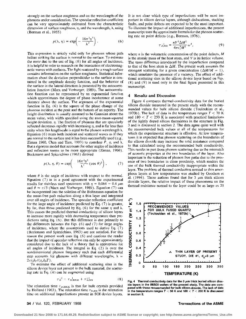
Figure 4 compares thermal-conductivity data for the buried silicon dioxide measured in the present study with the recommended values for bulk silicon dioxide (Touloukian et al., 1970b). The lack of data in the temperature ranges T < 70 K and 180 < T < 250 K is associated with practical limitations of the lightly doped silicon thermistors in the structure in Fig. 3 and is discussed in section 2. The data agree quite well with the recommended bulk values at all of the temperatures for which the experimental structure is effective. At low temperatures it is expected that phonon scattering on the boundaries of the silicon dioxide may increase the total resistance compared to that calculated using the recommended bulk conductivity. This results in part from phonon scattering due to the mismatch of acoustic properties at the two boundaries of the layer. Also important is the reduction of phonon free paths due to the presence of two boundaries in close proximity, which renders the use of the bulk thermal conductivity inappropriate within the layer. The problem of thermal conduction normal to thin amorphous layers at low temperatures was studied by Goodson et al. (1994). These authors found that for 3 lira thick silicon dioxide layers, the relative impact of these phenomena on the thermal resistance normal to the layer could be as large as 20
X 1.6
E 1.4
t 1.2
t 1 > 1
t-O 0.8 3 O Z 0.6 O O 0.4 _l < 2 0.2 oc m T U
I I 11 I I I I 11 I I I I I I I 11 I 1 1 1 • RECOMMENDED VALUES - FOR BULK FUSED QUARTZ
(Touloukian et al., 1970b)
I 1 1 1 iTl 1
THIN LAYER OF PRESENT •
STUDY, DIE # 1 , dQ=3 urn
• ' J_i_i_
I- 0 50 100 150 200 250 300 350
TEMPERATURE (K)
Fig. 4 Thermal conductivity data for the 3 jum thick buried silicon dioxide layers in the BESOI wafers of the present study. The data are compared with those recommended for bulk silicon dioxide. The lack of data in the temperature ranges T < 50 K and 180 < T < 250 K is discussed in section 2.
34 / Vol. 120, FEBRUARY 1998 Transactions of the ASME
Downloaded 21 Nov 2008 to 171.64.49.29. Redistribution subject to ASME license or copyright; see http://www.asme.org/terms/Terms_Use.cfm

and even 50 percent at temperatures 45 K and 20 K, respectively. These reductions in the effective oxide conductivity are treated as sources of uncertainty in the present work, and therefore augment the uncertainty in the extracted thermal conductivity of the silicon device layer. While the relative effect on the oxide resistance is quite large at 20 K, the contribution to relative uncertainty in the silicon conductivity at that temperature is considerably smaller, less than 24 percent. But the large uncertainty in the oxide resistance at the lowest temperatures contributes significantly to the uncertainty in the temperature of the structure during the measurement, and therefore influences the width of temperature error bars in subsequent plots.
Figure 5 shows thermal-conductivity data for the silicon device layers as a function of temperature. The maximum in the conductivity occurs near 70 K and separates the low-temperature region, where scattering is dominated by imperfections and surfaces, from the high temperature region, where phonon-phonon scattering is dominant. A portion of the recommended thermal conductivity curve for bulk silicon is provided for reference (Touloukian et al., 1970a). The recommended bulk conductivity reaches a much higher maximum, 5500 W m"1 K - 1
at the temperature of 30 K. The thermal conductivities of the silicon device layers are significantly lower than the values recommended for bulk samples due to the much stronger reduction of phonon mean free path by boundary scattering. The data clearly show that this effect is more prominent for thinner layers. The figure also shows the predictions calculated using the theory developed in Section 3. It must be emphasized that the predictions are not the result of fitting to the data, but rather are a prediction based only on the theory of Holland (1963) and the modification to account for boundary scattering. The only adjustable parameter is the roughness of the boundaries r\, which was estimated to be between 2 to 10 A for BESOI wafers (Maszara, 1991). The predicted thermal conductivity curves are plotted for r\ = 5 and 10 A. Increasing r] beyond 10 A has a negligible effect on the predicted thermal conductivity at temperatures down to 20 K, indicating that the use of r\ = 10 A effectively models completely diffuse scattering. The fraction of the phonons that are specularly reflected increases as the surface roughness dimension decreases, thus diminishing the impact of boundary scattering on the thermal conductivity. The effect of surface roughness is more significant at lower temperatures where the population of the long wavelength phonons increases. In this figure no additional scattering due to fabrication-related imperfections is introduced. Figure 5 shows that
100 TEMPERATURE (K)
4 0 0
PREDICTIONS BOUNDARY SCATTERING
BOUNDARY SCATTERING
2x1 017 VACANCIES cm"3
• Yu et al. (1996) A Zheng et al. (1996) A Savvides & Goldsmind (1973)
0.1 1 SILICON LAYER THICKNESS,
1 0 d (urn)
50
Fig. 5 Thermal conductivities of the silicon device layers with thicknesses 0.42, 0.83, and 1.6 /urn. The data are compared with the predictions of the phonon-boundary scattering analysis.
Fig. 6 Room-temperature thermal conductivity data for silicon layers as a function of their thickness. Also plotted are conductivity predictions that account for phonon-boundary scattering and phonon scattering on vacancies.
the data agree well with predictions for the 1.6 fxm thick silicon overlayer over the entire temperature range. The poorer agreement for the 0.42 fxm and 0.83 /im thick silicon layers may be due to the higher concentrations of imperfections associated with epitaxial silicon growth in these layers. BESOI device layers contain a large concentration of dislocations and stacking faults collected near the former interface with the heavily doped etch stop layer (Maszara, 1991). These imperfections may more strongly reduce the conductivity of thinner layers. The importance of scattering on these imperfections is nearly impossible to assess without more detailed information about the types of defects and the variation of their concentrations within layers.
Figure 6 shows the measured lateral thermal conductivities of silicon layers as a function of thickness near room temperature. The impact of phonon-boundary scattering is predicted using the theory described in section 3 and plotted as a solid line in the same graph. Previous experimental data for a 20 /um thick silicon specimen (Savvides and Goldsmid, 1973) and a 4 fim thick free-standing silicon film (Yu et al , 1996) are consistent with the predictions. However, the lateral thermal conductivity measured in a 0.15 fxm thick SIMOX device layer at temperatures between 330 and 380 K (Zheng et al., 1996) shows nearly two orders of magnitude reduction compared to the bulk value and is far below the predictions of the phonon-boundary scattering model. This disparity could be explained by a high concentration of lattice imperfections in the sample of Zheng et al. (1996) or by uncertainty in the measurements of the layer thickness or the thermal conductivity.
The lateral thermal conductivities measured in the BESOI device layers of the present study are consistent with the phonon-boundary scattering predictions. For the thickest layers the reduction is small and not experimentally significant, suggesting a microstructure and purity that closely resemble those in bulk crystals. This shows that thermal simulations of SOI transistors with device layers thicker than about 1.5 fim should use the thermal conductivity of bulk silicon. However, the bulk conductivity overpredicts the data for the thinnest silicon overlayer by nearly 40 percent, indicating a potential for a large error in device simulations. The reduction is significant even considering the experimental uncertainty and may be due to any of the mechanisms shown in Fig. 1. A strong reduction due to impurities is unlikely because the boron concentration in the device layer is below that at which the thermal conductivity of bulk crystals is reduced by scattering on impurities (Goodson and Cooper, 1995). While boundary scattering analysis yields predictions consistent with the data in Figs. 5 and 6, a more con-
Journal of Heat Transfer FEBRUARY 1998, Vol. 1 2 0 / 3 5
Downloaded 21 Nov 2008 to 171.64.49.29. Redistribution subject to ASME license or copyright; see http://www.asme.org/terms/Terms_Use.cfm

vincing confirmation of this model near room temperature will require data for thinner layers. The predominant additional imperfection in BESOI silicon device layers may be dislocations. Dislocations due to the epitaxial growth process are assumed to account for the observed warping of the device layer across a wafer (Ma et al., 1991) and provide a potential explanation for the difference in the thermal conductivity values obtained for samples on dies nos. 1 and 2. A study involving BESOI layers of thickness 0.1 /xm and below would be particularly helpful since the predicted relative conductivity reduction will exceed 60 percent. Data for such layers would not resolve the situation, however, because it would be difficult to ensure that the concentration of fabrication-related imperfections is the same in the layers of different thicknesses. Figure 6 includes a very approximate prediction of the effect of evenly distributed fabrication-related imperfections, which is based on Eqs. (8) and (9). A concentration of 2 X 10 " cnT3 vacancies can reduce the thermal conductivity by more than 10 percent.
5 Conclusions
The data provided in this manuscript are of practical importance for SOI technology and for MEMS that are made using SOI wafers. The data are needed most urgently for thermal simulation of SOI transistors that must withstand the temperature rise during ESD pulses. The impact of this study is greatest for silicon device layers thinner than about 0.5 fim, for which the relative reduction in the conductivity due to phonon-bound-ary scattering exceeds 40 percent. The reduction for SOI technologies with very thin device layers is more dramatic, as shown in Fig. 6. It must be noted that the temperature rise in active regions cooled by lateral conduction in the silicon actually scales with the inverse of the square root of the silicon thermal conductivity (Goodson and Cooper, 1995), such that the relative change in the temperature rise will be less than the relative reduction in the thermal conductivity.
The data and analysis documented here are also of considerable fundamental importance because they can be used to extract the phonon mean free path in silicon for shorter phonon wavelengths than has been possible previously. The Boltzmann equation solution used here relates the impact of boundary scattering on heat transport by phonons of a given wavelength to the ratio of the free path to the layer thickness. Since SOI wafers provide silicon layers that approach bulk silicon in purity and micro-structural perfection, the data provide the opportunity to determine the wavelengths of phonons that have free paths comparable to the layer thickness. The agreement of the predictions with the data provides an important confirmation of the free paths obtained by means of the conductivity integrals of Holland (1963).
Acknowledgments
The authors are warmly appreciative of the research group of J. D. Plummer for the use of the cryogenic stage. M. Asheghi appreciates the help of H. Khalkhali of University of Dayton with finite-element simulations of the temperature distribution in the experimental structure. This work was sponsored by the Semiconductor Research Corporation under contracts 97-SJ-461 and 96-PJ-357. K.E.G. appreciates support from the Office of Naval Research Young Investigator Program and the National Science Foundation through the CAREER Program and grant CTS-9622178.
References Amerasekera, A., Van Abeelen, W., Van Roozendaal, L., Hannemann, M.,
and Schofield, P., 1992, "ESD Failure Modes: Characteristics Mechanisms, and Process Influences," IEEE Trans. Electron Devices, Vol. 39, pp. 430-436.
Beckmann, P., and Spizzichino, A., 1963, The Scattering of Electromagnetic Waves from Rough Surfaces, Pergamon Press Inc., New York, pp. 29, 81.
Berman, R., 1976, Thermal Conduction in Solids, Oxford University Press, Oxford, United Kingdom, pp. 23, 73-75.
Berman, R., Foster, E. L., and Ziman, J, M., 1955, "Thermal Conduction in Artificial Sapphire Crystals at Low Temperatures," Proc. Roy. Soc. A, Vol. 231, pp. 130-144.
Callaway, J., 1959, "Model for Lattice Thermal Conductivity at Low Temperatures," Phys. Rev., Vol. 113, pp. 1046-1051.
Cellar, G. K., and White, A. E., 1992, "Buried Oxide and Silicide Formation by High-Dose Implantation in Silicon," MRS Bulletin, Vol. 17, No. 6, pp. 4 0 -46.
Chen, G., 1997, "The Size and Interface Effects on the Thermal Conductivity of Superlattices and Periodic Thin-Film Structures,'' ASME JOURNAL OF HEAT TRANSFER, Vol. 119, pp. 220-229.
Chen, G., and Tien, C. L„ 1993, "Thermal Conductivities of Quantum Well Structures," Journal of Thermophysics and Heat Transfer, Vol. 7, No. 2, pp. 311-318.
Chui, B. W., Stowe, T. D., Kenny, T. W„ Mamin, H.J., Terris, B.D., and Rugar, D., 1996, "Low-Stiffness Silicon Cantilevers for Thermal Writing and Piezoresistive Readback with the Atomic Force Microscope," Applied Physics Letters, Vol. 69, pp. 2767-2769.
Goodson, K. E., and Cooper, P. T., 1995,' 'The Effect of High-Energy Electrons on Lattice Conduction in Semiconductor Devices," Proceedings of the Symposium on Thermal Science and Engineering in Honor of Chancellor Chang-Lin Tien, R. Buckius, ed., Office of Printing Services, University of Illinois at Urbana-Champaign, pp. 153-159.
Goodson, K. E., Flik, M. I., Su, L. T„ and Antoniadis, D. A., 1993, "Annealing Temperature Dependence of Thermal Conductivity of CVD Silicon-Dioxide Layers," IEEE Electron Device Letters, Vol. 14, pp. 490-492.
Goodson, K. E„ Flik, M. I., Su, L. T., and Antoniadis, D. A., 1994, "Prediction and Measurement of the Thermal Conductivity of Amorphous Dielectric Layers," ASME JOURNAL OF HEAT TRANSFER, Vol. 116, pp. 317-324.
Goodson, K. E„ Flik, M. I., Su, L. T., and Antoniadis, D. A., 1995, "Prediction and Measurement of Temperature Fields in Silicon-on-Insulator Electronic Circuits," ASME JOURNAL OF HEAT TRANSFER, Vol. 117, pp. 574-581.
Holland, M. G., 1963, "Analysis of Lattice Thermal Conductivity," Phys. Rev., Vol. 132, No. 6, pp. 2461-2471.
Ma, D. I„ Campisi, J. G., Qadri, S. B., and Peckerar, M. C , 1991, "Characterization of Silicon on Insulator Substrates Using Reflection Mode Double-Crystal X-ray Topography," Thin Solid Films, Vol. 206, pp. 27-33.
Marx, E., and Vorburger, T. V., 1989, "Direct and Inverse Problems for Light Scattered by Rough Surfaces," Applied Optics, Vol. 29, No. 25, pp. 3613-3626.
Mastrangelo, C. H., and Miiller, R. S., 1988, "Thermal Diffusivity of Heavily Doped Low Pressure Chemical Vapor Deposited Polycrystalline Silicon Films," Sensors and Materials, Vol. 3, pp. 133-141.
Maszara, W. P., 1991, "Silicon-On-Insulator by Wafer Bonding: A Review," J. Electrochem. Soc, Vol. 138, No. 1, pp. 341-347.
Paul, O.M., Korvink, J., and Baltes, H., 1993, "Thermal Conductivity of CMOS Materials for the Optimization of Microsensors," Journal of Micromecha-nics and Microengineering, Vol. 3, No. 3, pp. 110-12.
Paul, O. M., Korvink, J., and Baltes, H., 1994, "Determination of the Thermal Conductivity of CMOS IC Polysilicon," Sensors and Actuators A (Physical), Vol. A41, No. 1-3, pp. 161-164.
Peters, L., 1993, "SOI Takes Over Where Silicon Leaves Off," Semiconductor International, Vol. 16, pp. 48-51 .
Savvides, N., and Goldsmid, H. J., 1973, "The Effect of Boundary Scattering on the High-Temperature Thermal Conductivity of Silicon," J. Phys. C: Solid State Phys., Vol. 6, pp. 1701-1708.
Sondheimer, E. H., 1952, "The Mean Free Path of Electrons in Metals," Adv. Phys., Vol. 1, pp. 1-42.
Tai, Y. C , Mastrangelo, C. H., and Mtlller, R. S., 1988, "Thermal Diffusivity of Heavily Doped Low-Pressure Chemical Vapor Deposited Polycrystalline Silicon Films," J. Appl. Phys., Vol. 63, pp. 1442-1447.
Touloukian, Y. S., Powell, R. W., Ho, C. Y„ and Klemens, P. G„ 1970a, "Thermal Conductivity of Metallic Elements and Alloys,'' Thermophysical Properties of Matter, Vol. 1, New York: IFI/Plenum, p. 333, 339.
Touloukian, Y. S., Powell, R. W., Ho, C. Y„ and Klemens, P. G., 1970b, "Thermal Conductivity of Nonmetallic Solids," from Thermophysical Properties of Matter, Vol. 2, IFI/Plenum, New York, p. 193.
Von Arx, M„ and Baltes, H., 1992, "A Microstructure for Measurement of Thermal Conductivity of Polysilicon Thin Films," Journal of Microelectromecha-nical Systems, Vol. 1, No. 4, pp. 193-6.
Von Arx, M„ Paul, O. M„ and Baltes, H„ 1995, "Determination of the Heat Capacity of CMOS Layers for Optimal CMOS Sensor Design," Sensors and Actuators A (Physical), Vol. A47, No. 1-3, pp. 428-31.
Yu, X. Y., Zhang, L., and Chen, G„ 1996, "Thermal-Wave Measurement of Thin-Film Thermal Diffusivity with Different Laser Beam Configurations," Rev. Sci. Instrum., Vol. 67, No. 6, pp. 2312-2316.
Zheng, X. Y„ Li, S., Chen, M„ and Wang, K. L„ 1996, "Giant Reduction in Lateral Thermal Conductivity of Thin Nitride/Silicon/Oxide Membrane Measured with a Micro Thermal Bridge," Proc. Int. Mech. Eng. Congress and Exp., C. T. Avedisian et al„ eds., ASME, New York, pp. 93-98.
Ziman, J. M., 1960, Electrons and Phonons, Oxford University Press, Oxford, United Kingdom, pp. 456-460.
36 / Vol. 120, FEBRUARY 1998 Transactions of the ASME
Downloaded 21 Nov 2008 to 171.64.49.29. Redistribution subject to ASME license or copyright; see http://www.asme.org/terms/Terms_Use.cfm