tcad design of tunnel fet structures and extraction of ... design of tunnel fet structures and...
TRANSCRIPT
International Journal of Science and Research (IJSR) ISSN (Online): 2319-7064
Index Copernicus Value (2013): 6.14 | Impact Factor (2013): 4.438
Volume 4 Issue 7, July 2015
www.ijsr.net Licensed Under Creative Commons Attribution CC BY
TCAD Design of Tunnel FET Structures and
Extraction of Electrical Characteristics
Ashwin S Raj1, Sreejith S
2, Sajeshkumar U
3
1, 2, 3VLSI & Embedded Systems Lab, Govt. College of Engineering Kannur, Mangattuparamba, Kerala 670563, India
Abstract: Silicon dioxide (SiO2) or silica is a metal oxide which comes under fourth group. The properties of SiO2 includes high
thermal stability, good abrasion resistance and good electrical insulation. It is the most commonly used dielectrics in semi- conductor arena. Hafnium oxide (HfO2) comes under the group of high-k dielectrics. This inorganic compound, which is also known as hafnia acts as a replacement for conventional silicon dioxide dielectric layers. In this paper, we have simulated TFET structures with hafnia and silica as dielectric materials. A considerable increase in capacitance, of around 58%, was obtained when we c h a n g e d the dielectric material from silica to hafnia. The dimensions of dielectric layer was kept constant during the simulations. The gaussian doping distribution is very much similar to real doping profiles and is simple in structure. So we adopted gaussian doping profile for source and drain doping. The simulations results showed that TFET structures with SiO2 dielectric layer exhibited better transfer
characteristics than TFET structures with HfO2 dielectric layer.
Keywords: Tunnel FETs, Gaussian doping, Subthreshold swing, Sentaurus TCAD
1. Introduction The scaling down of conventional MOSFET [1] becomes more difficult beyond the range of 30nm. The Ion/Ioff
ratio of conventional MOSFET [5] [6] is reduced by scaling down, due to the physical limitations of the device. Also, manufacturing of MOSFETs which can be switched off, becomes more difficult. Direct quantum mechanical tunneling occurs when the channel length approaches 10nm and makes t h e switching off impossible. Tunnel FETs [2], the next generation of MOSFETs are based on the concept of using tunneling instead of avoiding tunneling. Tunneling helps TFETs to achieve a subthreshold swing below 60 mv/dec. Conventional MOSFETs are limited by Maxwell-Boltzmann tail of carriers defined b y :
(1)
where εi is the energy of ith
level, Ni is the no of carriers in
the set of states with energy εi, gi is the degenerancy of
energy level i, µ is the chemical potential, k is the boltz-
mann’s constant and T is the absolute temperature. Hence the
conventional MOSFETs exhibits a subthreshold swing above
60 mv/dec. Conventional MOSFETs and TFETs are similar
in structure, but the doping of source and drain terminals
are different for these devices. Source and drain terminals of
conventional MOSFETs are doped of same type, while the
source and drain terminals of TFETs are doped of opposite
type.
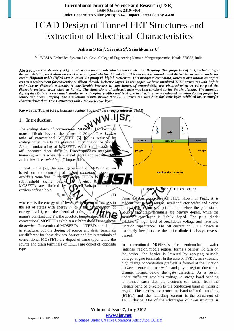
Figure 1: Basic TFET structure
From the basic structure of TFET shown in Fig.1, it is
evident that p-type source, semiconductor wafer and n-type
drain together forms a p-i-n diode below the gate stack.
Source and drain terminals are heavily doped, while the
semiconductor layer is lightly doped. The p-i-n diode
exhibits a high level of breakdown voltage and have low
junction capacitance. The off current of TFET device is
extremely low, because the p-i-n diode is always reverse
biased.
In conventional MOSFETs, the semiconductor wafer
(intrinsic region/middle region) forms a barrier. To turn on
the device, the barrier is lowered by applying suitable
voltage at gate terminals. In the case of TFETs, an extremely
high charge concentration gradient is formed at the junction
between semiconductor wafer and p-type region, due to the
channel formed below the gate dielectric. As a result,
under sufficient gate bias voltage, a strong band bending
is formed such that the electrons can tunnel from the
valence band of p-region to the conduction band of intrinsic
region. This process is termed as band-to-band tunneling
(BTBT) and the tunneling current is the on-current of
TFET device. One of the advantages of p-i-n structure is
Paper ID: SUB156931 2447
International Journal of Science and Research (IJSR) ISSN (Online): 2319-7064
Index Copernicus Value (2013): 6.14 | Impact Factor (2013): 4.438
Volume 4 Issue 7, July 2015
www.ijsr.net Licensed Under Creative Commons Attribution CC BY
that, it exhibits highest diffusion barrier that can be
achieved through degenerate doping. Due to this property,
the scaling down of TFETs are very much easier than that
of conventional MOSFETs.
2. Subthreshold Swing and ON Current of
TFETs
Drain to source saturation current or on current (Ion) of
TFETs [3] [4] are given b y :
(2)
where µn is the electron surface mobility of the channel, Cox
is the dielectric capacitance, W is the channel width, L is the
channel length, Vgs is the maximum value of applied gate-
to-source voltage, Vth is the threshold voltage and λ is the
channel length modulation coefficient.
If channel length modulation coefficient equals zero,
equation (2) can be rewritten as f o l l o w s :
(3)
Subthreshold swing/subthreshold slope can be defined as the
gate voltage required to change drain to source current by
one decade. It can be determined as the inverse of slope
of the log Ids vs Vgs curve, in the subthreshold exponential
r e g i o n , as shown in Fig. 2.
Figure 2: Subthreshold swing
A theoretical approximation of subthreshold swing is given
below:
(4)
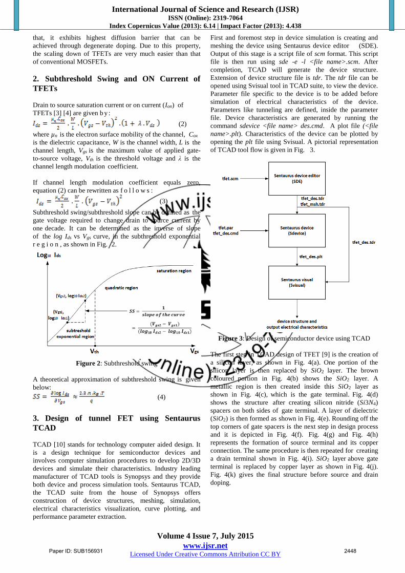
3. Design of tunnel FET using Sentaurus
TCAD
TCAD [10] stands for technology computer aided design. It
is a design technique for semiconductor devices and
involves computer simulation procedures to develop 2D/3D
devices and simulate their characteristics. Industry leading
manufacturer of TCAD tools is Synopsys and they provide
both device and process simulation tools. Sentaurus TCAD,
the TCAD suite from the house of Synopsys offers
construction of device structures, meshing, simulation,
electrical characteristics visualization, curve plotting, and
performance parameter extraction.
First and foremost step in device simulation is creating and
meshing the device using Sentaurus device editor (SDE).
Output of this stage is a script file of scm format. This script
file is then run using sde -e -l <file name>.scm. After
completion, TCAD will generate the device structure.
Extension of device structure file is tdr. The tdr file can be
opened using Svisual tool in TCAD suite, to view the device.
Parameter file specific to the device is to be added before
simulation of electrical characteristics of the device.
Parameters like tunneling are defined, inside the parameter
file. Device characteristics are generated by running the
command sdevice <file name> des.cmd. A plot file (<file
name>.plt). Characteristics of the device can be plotted by
opening the plt file using Svisual. A pictorial representation
of TCAD tool flow is given in Fig. 3.
Figure 3: Design of semiconductor device using TCAD
The first step in TCAD design of TFET [9] is the creation of
a silicon layer, as shown in Fig. 4(a). One portion of the
silicon layer is then replaced by SiO2 layer. The brown
coloured portion in Fig. 4(b) shows the SiO2 layer. A
metallic region is then created inside this SiO2 layer as
shown in Fig. 4(c), which is the gate terminal. Fig. 4(d)
shows the structure after creating silicon nitride (Si3N4)
spacers on both sides of gate terminal. A layer of dielectric
(SiO2) is then formed as shown in Fig. 4(e). Rounding off the
top corners of gate spacers is the next step in design process
and it is depicted in Fig. 4(f). Fig. 4(g) and Fig. 4(h)
represents the formation of source terminal and its copper
connection. The same procedure is then repeated for creating
a drain terminal shown in Fig. 4(i). SiO2 layer above gate
terminal is replaced by copper layer as shown in Fig. 4(j).
Fig. 4(k) gives the final structure before source and drain
doping.
Paper ID: SUB156931 2448

International Journal of Science and Research (IJSR) ISSN (Online): 2319-7064
Index Copernicus Value (2013): 6.14 | Impact Factor (2013): 4.438
Volume 4 Issue 7, July 2015
www.ijsr.net Licensed Under Creative Commons Attribution CC BY
Figure 4: Design steps of tunnel FET
4. Gaussian Doping
The structure of 2D Gaussian doping functions are simple
and is very much similar to real doping profiles. Gaussian
doping profile [11] is defined by these parameters: peak
doping (N ), lateral peak position (x0), horizontal peak
position (y0), lateral peak length (∆x), lateral standard
deviation (σx) and horizontal standard deviation (σy ).
The 2D Gaussian doping distribution is the superimposition
of Gaussian doping distributions along x and y directions and
a constant background doping. The governing equations
for Gaussian doping along x and y directions are given
below:
(5)
(6)
Fig. 5 and Fig. 6 shows typical Gaussian doping
distribution curves. The parameters are assumed as
f o l l o w s :
• N = 10/cm3
• x0 = 0 units
• y0 = 0 units
• σx = 0.4 units
• σy = 0.4 units
Figure 5: Gaussian doping along x-direction
Figure 6: Gaussian doping along y-direction
5. Tunnel FET Simulation
A tunnel FET with dimensions as described below was
designed as a 2D device using Sentaurus TCAD. Simulated
structure of TFET is shown in Fig. 7.
Figure 7: Simulated TFET structure
Total device length: 0.23 µm
Total device height: 2.237 µm
Source doping: 3 ×10²⁰ per cm3
Drain doping: 3 ×10²⁰ per cm3
Substrate doping: 1 ×10¹³ per cm3
Gaussian doping depth: 0.01
Gaussian doping factor: 0.8
The SiO2 dielectric layer was then replaced by hafnium
dioxide (HfO2) layer of same dimensions in order to
increase the capacitance. Simulations was then repeated for
the TFET structure with HfO2 as dielectric layer. The
simulation results are shown in Fig. 9. For the TFET
structure with HfO2 as dielectric, a Gaussian doping
thickness of 0.01 was found to be the optimized parameter.
For this gaussian doping thickness, an Ion of 0.18 nA, Ioff of
0.014 pA, threshold voltage of 0.9 V was obtained. The
curve exhibited a SS of 46 mv/dec.
Paper ID: SUB156931 2449

International Journal of Science and Research (IJSR) ISSN (Online): 2319-7064
Index Copernicus Value (2013): 6.14 | Impact Factor (2013): 4.438
Volume 4 Issue 7, July 2015
www.ijsr.net Licensed Under Creative Commons Attribution CC BY
Figure 7: Transfer characteristics with SiO2 as dielectric
Figure 9: Transfer characteristics with HfO2 as dielectric
6. STBFET Simulation Basic Sandwich tunnel barrier FET (STBFET) structure is
shown in Fig. 10.
Figure 10: Basic STBFET structure
The modified structure of TFET, sandwich tunnel barrier
FET (STBFET) [8] was designed as a scaled down version
of TFET. The overall size of STBFET is low when compared
to that of TFET. STBFET consists of a source region
sandwiched in between two drain regions. The device
parameters are given below. TCAD simulated structure of
STBFET is shown in Fig. 11.
Total device length: 0.23 µm
Total device height: 0.119 µm
Source doping: 2 ×10²⁰ per cm3
Drain doping: 5 ×10¹⁹ per cm3
Substrate doping: 1 ×10¹³ per cm3
Gaussian doping depth: 0.01
Gaussian doping factor: 0.8
Dielectric: SiO2
Transfer characteristics of STBFET is shown in Fig.
10. Fig. 11 gives the log plot for SS calculation of STBEFT.
There was no variation in transfer characteristics when
Gaussian doping depth of STBFET was varied. A very high
ON current (1.4 µA) was obtained for STBFET when
compared to that of planar TFET. Simulated values of
electrical characteristics of STBFET are shown below.
ON current (ION ): 1.4 µA
OFF current (IOF F ): 7.0 pA
Threshold voltage (Vth): 0.76 V
Subthreshold swing (SS): 36 mv/dec
Figure 10: Transfer characteristics of STBFET
Figure 11: Log plot for SS calculation of STBFET
STBFET offered a very much low SS of 36 mv/dec com-
pared to 42 mv/dec SS of TFET. This implies that, turn
ON time of STBFET is less than that of TFET. A very
Paper ID: SUB156931 2450

International Journal of Science and Research (IJSR) ISSN (Online): 2319-7064
Index Copernicus Value (2013): 6.14 | Impact Factor (2013): 4.438
Volume 4 Issue 7, July 2015
www.ijsr.net Licensed Under Creative Commons Attribution CC BY
high ON current obtained for STBFET shows that it is a
promising candidate in the FET arena .
7. Conclusion
With the dimensions of dielectric layer remaining the same,
the silicon dioxide seems to be a better dielectric than
hafnium dioxide. At an increased capacitance level, the
simulated results of Hf O2 shows fluctuations, although the
device is expected to deliver better ON current as per the
drain current equation. A smooth transition was observed in
the case of TFET structures with SiO2 as dielectric. The
optimized Gaussian doping depth for TFET with SiO2 as
dielectric is 0.0005 and for TFET with HfO2 dielectric layer,
the optimized value is 0.01. Compared to the peak ON
current value of 0.18 nA obtained by using HfO2 as
dielectric, a greater value of 4.8 nA was obtained when using
SiO2 as dielectric. An increase in capacitance thus resulted
in degradation of ON current of the device. The STBFET,
have much higher ION –to–IOF F ratio com- pared with the
MOSFETs and traditional TFETs. Due to the specific
device topology employed in STBFET, the device shows
several distinct advantages. The tunneling current in this
device scales with the gate area, instead of gate width
leading to high ION . IOF F , is essentially dependent on spacer
thickness and is very low. STBFET have an excellent output
current saturation
References
[1] J.P. Collinge, “Finfets and other multigate transistors”,
Springer, 2007. [2] Mathias Born, “Vertical Gate Controlled Tunnel
Transistors in Si and SiGe”, Cuvillier Verlag, 2007.
[3] Joachim N. Burghartz, “Guide to State of the Art
Electron Devices”, John Wiley & Sons, 2013. [4] Simon Deleonibus, “Intelligent Integrated Systems:
Devices, Technologies, and Architectures”, CRC
Press, 2014. [5] Narain D. Arora, “MOSFET Models for VLSI Circuit
Simulation: Theory and Practice”, Springer Science
& Business Media, 2012. [6] R. M. Warner, B. L. Grung, “MOSFET Theory and
Design”, Oxford University Press, 1999.
[7] Pei- Yu Wang and Bing- Yue Tsui, “Epitaxial
tunnel layer structure for p-channel tunnel FET
improvement”, IEEE transactions on electronic devices.
Vol. 60, Issue 12, December 2013. [8] Ram Asra and Mayank Srivastava, “A tunnel FET for
VDD scaling below 0.6 V with a CMOS-comparable
performance”, IEEE transactions on electronic devices.
Vol. 58, Issue 7, July 2011.
[9] Boucart. K and Ionescu. A.M, “Double-gate tunnel FET
with high-k gate dielectric”, IEEE transactions on
electronic devices. Vol. 54, Issue 7, July 2007. [10] Sentaurus TCAD manual [online]. Available:
http://www.synopsys.com/tools/tcad/capsulemodule/sent
aurus_ds.pdf [11] Michael Stockinger, Optimization of ultra low power
CMOS transistors [online].Available:
http://www.iue.tuwien.ac.at/phd/stockinger/node24.html
Author Profile
Ashwin S Raj is a PG student at the Department of
Electronics and Communication Engineering, Govt.
College of Engineering, Kannur. He received his B.
Tech degree with Electrical and Electronics
Engineering specialization from Calicut University in
2013.
Sreejith. S is an Assistant Professor at the De-partment
of Electronics and Communication En-gineering, Govt.
College of Engineering, Kannur. He received his B.
Tech degree in Electronics and Communication
Engineering from Calicut University in 1997 and his
M. Tech degree in VLSI design from NIT Surathkal in 2014.
Sajeshkumar. U is an Assistant Professor at the
Department of Electronics and Communication En-
gineering, Govt. College of Engineering, Kannur. He
received his B. Tech degree in Electronics and
Communication Engineering from Calicut University
in 2001 and his M. Tech degree NIT Calicut in 2010.
Paper ID: SUB156931 2451