synchronous design flow for globally asynchronous · pdf fileglobally asynchronous locally...
TRANSCRIPT
Proceedings of the 10th WSEAS International Conference on CIRCUITS, Vouliagmeni, Athens, Greece, July 10-12, 2006 (pp64-69)
Synchronous Design Flow for
Globally Asynchronous Locally Synchronous Systems
JONAS CARLSSON, KENT PALMKVIST, and LARS WANHAMMAR
Department of Electrical Engineering
Linköping University
SE-581 83 Linköping
SWEDEN
http://www.es.isy.liu.se/
Abstract: – In this paper, we introduce an efficient design flow for Globally Asynchronous Locally
Synchronous systems, which can be used by designers without prior knowledge of asynchronous circuits. The
design flow starts with a high-level description model of the system in Simulink and ends with a hardware
implementation in an FPGA or a standard-cell ASIC. We have developed a tool in MATLAB, so that the
designer easily can include asynchronous logic in a conventional synchronous design flow. The proposed
design flow is currently used for implementing the physical layer for a wireless LAN.
Key-Words: – GALS, Design flow, Asynchronous, FPGA, Simulink
1 Introduction
The scaling of the process geometries of CMOS
allows the designer to include more and more func-
tionality on the chip. However, this causes problems
since signals on adjacent wires interact due to cross
coupling and the wire delay increases for global
wires [1]. The interconnect effects makes it prob-
lematic to transfer information over long distances
in one clock period. By dividing a system into
smaller modules with up to 50 000 gates in each
module, the local interconnect problem is
alleviated [2]. By partitioning the system into
module with their own private clock domain and use
a robust communication scheme between modules,
it is possible to reduce the design effort of the global
clock (e.g., mesochronous clocking scheme). It is
also possible to remove the global clock and use an
asynchronous communication scheme between
locally clocked domains [3], called Globally Asyn-
chronous Locally Synchronous (GALS) scheme.
We use an asynchronous wrapper to separate the
synchronous modules into timing independent clock
domains. This results in a synchronous module that
can be modified without affecting the rest of the
system. This allows design groups to work concur-
rently and independently on different synchronous
modules. Furthermore, it supports reuse of synchro-
nous modules and IP blocks.
Asynchronous circuits are in general more chal-
lenging to design than synchronous circuits. A
synchronous circuit is timed by the system clock and
it does not matter if glitches occur in the synchro-
nous circuit as long as the glitch is not sampled by
the receiving register. A glitch in an asynchronous
circuit may be fatal, depending on the used scheme.
Asynchronous design flows are also lacking the
multitude of design tools that exists in a synchro-
nous design flow. An overview of asynchronous
design methodologies is given by S. Hauck in [4].
We advocate that the most important benefit of
the GALS based approach is the increased design
efficiency, which is obtained by the inherent divide-
and-conquer method. In this work, we have devel-
oped a design flow for GALS systems that can be
used by a designer who have no prior knowledge of
how to design asynchronous circuits.
Our tool written in MATLAB targets Altera's
Stratix II FPGA, but it can be extended to work with
ASICs and other FPGAs. The used asynchronous
handshake port in this work, have previously been
tested in an Xilinx Virtex II FPGA [5]. In this paper,
we have focused on FPGA, because of the short
turn-around-time. However, the principle of the
design flow used for FPGA or ASIC is the same.
The paper is organized as follows: Section 2
gives an overview of GALS, Section 3 shortly
describes the used design for the design flow and
Section 4 describes the design flow used for imple-
menting a GALS system.
2 Globally AsynchronousLocally Synchronous Systems
In this paper, we refer to GALS as a digital system
partitioned into modules with their private clock

Proceedings of the 10th WSEAS International Conference on CIRCUITS, Vouliagmeni, Athens, Greece, July 10-12, 2006 (pp64-69)
domains with unrelated clock frequencies. Each
clock domain is locally synchronous and may
locally generate its own clock signal using a local
oscillator. An asynchronous communication scheme
is used to communicate between clock domains. To
handle the asynchronous communication between
units, an asynchronous wrapper is added around
each synchronous module. The asynchronous
wrapper can be equipped with functions, such as a
local clock, communication ports, tunable voltage
supply, level-shifters, testing circuits, and FIFOs [6].
In Fig. 1, a generic asynchronous wrapper with a
synchronous module is illustrated.
In a GALS system, advantages are found in that
both asynchronous and synchronous techniques can
be mixed. The synchronous modules are designed
using conventional synchronous design tools. The
communication scheme between different clock
domains uses an asynchronous communication
scheme, which have the advantage that the transmit-
ting and the receiving module does not have to know
exactly when data will be transferred. The hand-
shake scheme acts as a rendezvous for the trans-
mitter and the receiver units.
GALS have been used in several ASIC imple-
mentations. F.K. Gürkaynak et al. [7] implemented a
GALS bus chip and M. Krstic et al. [8] implemented
a baseband processor for wireless LAN. The design
used in our work is similar to the design used in [8],
with the difference that we use a design flow from a
high-level description down to an implementation in
an FPGA, which is further described in Section 4.
F.K. Gürkaynak et al. [7] has developed a tool called
moduleassembler that helps to automate the design
flow for GALS in an ASIC design. However, the
local clock generation is still handled outside this
tool and the designer still have to have knowledge
about asynchronous ports and how different ports
can be combined.
3 IEEE 802.11a
We have used the standard IEEE 802.11a [9] as an
example for the design flow. IEEE 802.11a specifies
the physical layer of a wireless LAN. The standard
is based on Orthogonal Frequency Division Multi-
plexing (OFDM) and supports different data rates
from 6 Mbit/s up to a maximum of 54 Mbit/s (raw
bit rate). The physical layer includes channel
encoding/decoding, modulation/demodulation and
synchronization.
For the development of the design flow for a
GALS system, we have selected IEEE 802.11a for
the principles of data rate changes.
3.1 Implementation aspectsFigure 2 shows the block diagram of an IEEE
802.11a transmitter. For a specific bit rate (i.e., 6
Mbit/s to 54 Mbit/s), the rate of the data flowing
between computation blocks is different. This must
be handled by the state machine in the transmitter so
that a computation block does not run out of data.
The computation blocks in Fig. 2 have been
partitioned into different clock domains, which are
represented by dotted boxes. An asynchronous
wrapper is used to handle the asynchronous commu-
nication between domains. Blocks that communicate
through an asynchronous communication channel
(e.g., the convolution encoder and the interleaver)
can use simplified state machines, because the
communication channel will automatically handle
the data flow between these blocks. With help of the
asynchronous wrapper, the state machine in the
interleaver does not have to consider whether the
convolution encoder can send data. The wrapper for
the interleaver stops the local clock until the convo-
lution encoder sends data.
It is relatively easy to handle the data rate differ-
ences in a synchronous implementation of IEEE
802.11a. However, for a more complicated system,
GALS has an advantage in that neither the sending
synchronous module nor the receiving synchronous
module have to know if the other domain is ready to
receive or send data.
4 Design Flow
The GALS design flow is shown in Fig. 3. We have
omitted the iterative loops that exist between
different phases in the design flow to reduce the
number of edges in the figure.
The IEEE 802.11a PHY is modeled in Simulink
and the implementation is targeting an Altera
Stratix II FPGA [10]. We have chosen Simulink/
MATLAB from MathWorks [11], to model the
system and to generate the asynchronous wrapper.
Fig. 1: Asynchronous wrapper with a synchronous module.
Vdd gen.Clk gen.
DATAi
ACKi
DATAi+1
ACKi+1
TEST BUS
RATE REQUIREMENTi
Synchronousmodule
BIST

Proceedings of the 10th WSEAS International Conference on CIRCUITS, Vouliagmeni, Athens, Greece, July 10-12, 2006 (pp64-69)
4.1 System DesignSimulink is a model design and simulation tool for
model-based designs, which is integrated with
MATLAB. It is easy to build a system model using
predefined functions from MATLAB or blocks from
Simulink. A top-down design approach can be used
in Simulink to create several models of the design.
Starting with a high-level description model of the
system that defines the behavior of the system, we
add more implementation aspects to the model as it
gets closer to the HDL phase, and we end with a bit
true model.
As a starting point for our Simulink model, we
used a demonstration model supplied with Simulink,
which have some similarities with the IEEE 802.11a
standard. This model has been developed so that it
supports the physical layer for IEEE 802.11a. Our
last model in Simulink is a bit true model, which
uses bit true MATLAB models of the FFT and IFFT
from Altera. The final Simulink model will be used
as a reference model in the rest of the implementa-
tion phase to generate test data and reference data.
4.1.1 Clock domain partition
In the HDL phase in Fig. 3, computation blocks are
divided into different clock domains. The decision
on how to partitioning the system into clock
domains can be obtained in Simulink. A starting
point to divide a system into clock domains is to
merge blocks with high intercommunication rates in
the same clock domain and separate blocks with low
intercommunication rates into different clock
domains. Blocks, which have a variable data rate, as
mentioned in Section 3.1, can be divided into sepa-
rated clock domains to let the asynchronous wrapper
handle the data flow.
4.2 Asynchronous Wrapper GenerationSo far, the GALS design flow is the same as the
synchronous design flow. The difference is the HDL
phase in which the design includes the asynchronous
wrappers to handle the asynchronous communica-
tion between clock domains.
Most synchronous designers have no or little
knowledge of how to design a functional asynchro-
nous wrapper. Therefore, we have developed a tool
in MATLAB that generates the necessary compo-
nents for the asynchronous wrapper so that a
designer can use GALS without designing any asyn-
chronous circuits. The tool in MATLAB generates
the following components:
• Behavioral model for asynchronous wrappers
to be used in the HDL phase.
• Verilog Quartus Mapping file (.vqm) that
describes the logic circuitry used in the
asynchronous wrapper in terms of D flip-flops
and lookup tables.
• Quartus Setting File (.qsf) contains the
constrains to the place and route tool, on how
the logic is relatively placed in the
asynchronous wrapper.
• A second .qsf file for each asynchronous
channel used, that sets up constraints for the
timing analysis in the place and route tool.
The asynchronous wrappers are skipped in the
synthesis phase of the design flow. Hence, there are
no files generated for the synthesis part of the design
flow.
Fig. 2: IEEE 802.11a transmitter, divided into four clock domains.
ConvolutionencoderScrambler Interleaver
Pilots
Longpreamble
Modulationmapping
IFFTCyclicprefix
Windowing
Shortpreamble
Fig. 3: The design flow.
Asynchronous wrappergeneration
MATLAB
GALS System
HDL
Place & Route
Quartus II
Synthesis
Precision RTL
System Design
Simulink
Modelsim
Simulation
FPGA
Stratix II
Timing Analyser
Power Analyser
B
ehavior
Quartu
sSettin
g
Verilo
gQuartu
sMapping
Proceedings of the 10th WSEAS International Conference on CIRCUITS, Vouliagmeni, Athens, Greece, July 10-12, 2006 (pp64-69)
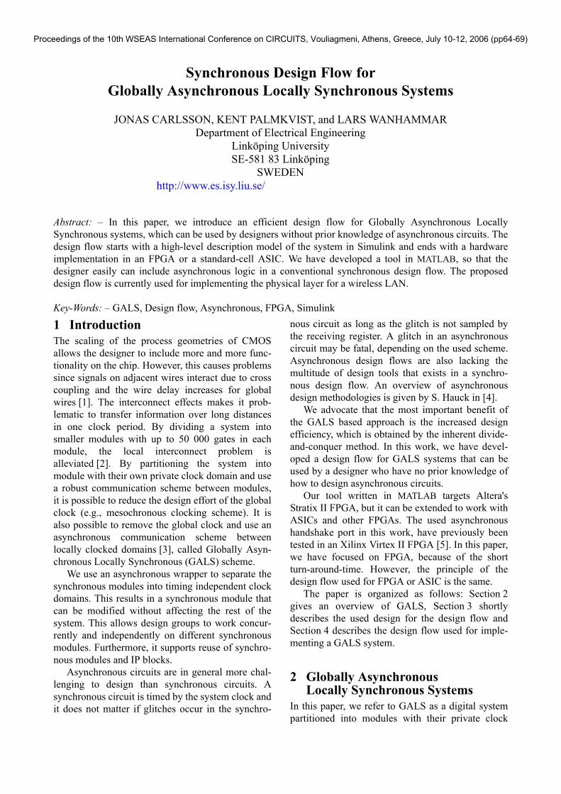
4.3 Asynchronous ChannelBetween each communicating unit, there is an asyn-
chronous communication channel. The channel typi-
cally consists of an active port and a passive port,
where one is a data input port and the other is a data
output port.
The tool in MATLAB, by default, generates active
output ports, passive input ports and dual-rail
signaling for the asynchronous wrapper. The default
asynchronous communication channel is shown in
Fig. 4. The designer only has to specify the size of
the data bus and the number of inverters in the local
ring oscillator. Hence, the designer does not have to
consider the details in the asynchronous handshake
circuits.
Designers who have knowledge in asynchronous
handshake schemes have the opportunity to select
between single-rail/dual-rail and active/passive
input/output ports respectively. Single-rail and dual-
rail signaling is further described in Section 4.7.
4.4 Asynchronous Wrapper
In Fig. 5, a simple asynchronous wrapper is illus-
trated. The wrapper has one input port and one
output port and internally a local clock. The designer
does not need to understand the internal circuits of a
wrapper, only how it is used by the synchronous
module to send and receive data to and from other
synchronous modules. Our asynchronous communi-
cation ports receive or transmit data each time an
enable signal (Enx) makes a high-to-low or low-to-
high transition [12]. This is the only signal that has
to be handled by the synchronous module to transfer
data between clock domains using the asynchronous
wrapper. The wrapper handles the communication to
other domains in a safe way that do not introduce
problems with metastability, which otherwise is a
problem when communication between clock
domains with different clock frequencies [13]. The
asynchronous wrapper stops the local clock when
data is to be sent or received, and the local clock is
started again when all data has been sent or received.
An example of communication between two
synchronous modules using the communication
channel shown in Fig. 4 is shown in Fig. 6. Both
modules transfer data the first two clock cycles. In
dual-rail signaling, d.t and d.f represents one and
zero data, respectively.
4.5 HDLThe translation to HDL code is currently done
manually, but a Simulink-to-VHDL converter [14]
can be used to translate from a Simulink model to a
HDL model.
There are FPGA vendor specific tools in
Simulink, which can be used to implement the
design in an FPGA using Simulink, such as DSP
Builder from Altera [10] and System Generator
from Xilinx [15]. Both these tools generate HDL
code using special blocksets in Simulink that are
specific to the vendors FPGAs. In our case, we want
to include asynchronous wrappers into the design,
which can be complicated using the design flow of
these tools because of the asynchronous circuits.
However, it may be possible to implement parts of
the synchronous design using these tools.
In the HDL phase, the design is described as a
GALS system. The design has been divided into
clock domains and has asynchronous communica-
tion between clock domains using the generated
asynchronous wrappers. With help of the behavior
description of the asynchronous wrappers and asyn-
Fig. 4: Asynchronous communication channel.
EnB1Ack
Data
EnA2
Activeport
Passiveport
Communicationchannel
ClkA ClkB
Clockdomain A
Clockdomain B
Fig. 5: An example of an asynchronous wrapper.
Fig. 6: Communication between two synchronous modules.
Clk
En2En1 Ack2
Data2Data1
Ack1
SynchronousModule
AsynchronousWrapper
Port 1 Port 2
ClkA
ClkB
EnA2
EnB1
d.t
Ack
d.f
Proceedings of the 10th WSEAS International Conference on CIRCUITS, Vouliagmeni, Athens, Greece, July 10-12, 2006 (pp64-69)
chronous communication channels, the designer can
focus on the implementation of the synchronous
modules.
4.6 Synthesis
Synthesis is only performed on the synchronous part
of the design and each synchronous module is
synthesized individually. In general, conventional
synchronous synthesis tool does not handle asyn-
chronous circuits correctly. However, it is possible
to use attributes in the HDL code to keep the
synthesis tool from modifying the asynchronous
circuitry, e.g., attributes such as dont_touch or
preserve_signal.
All asynchronous communication ports have a
clocked register to store data coming in or going out
of the communication port. These registers have to
be accounted for in the synthesis when setting up the
timing constraints. These registers guarantee that the
data are stable when transferred through the channel
or read by the synchronous module, respectively.
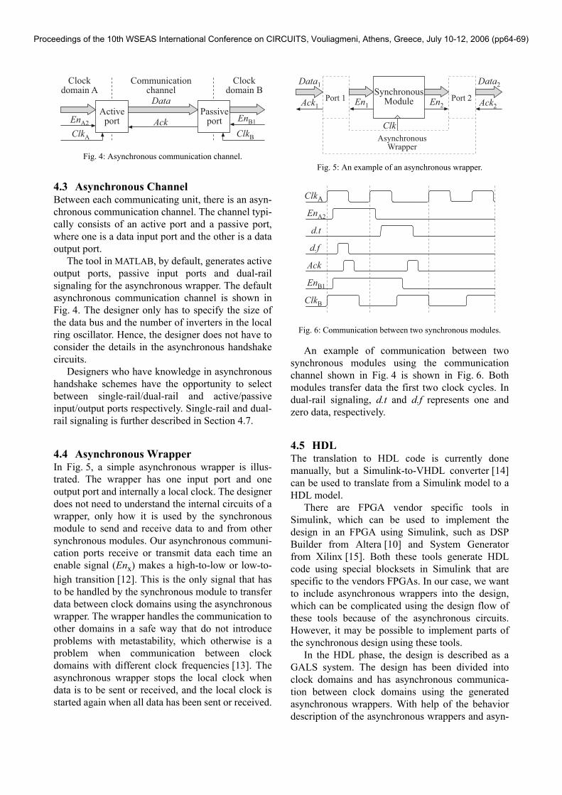
4.7 Place and Route
The logic description of the asynchronous wrappers
is included together with the placement and timing
information in the place and route tool.
The logic for the asynchronous wrappers have
fixed relative placement and the place and route tool
only has to place the asynchronous wrapper blocks
and route the signals used by the asynchronous
wrapper.
For a synchronous signal, there is a timing
window, in which the signal must arrive at its desti-
nation, this sets constrains on how long a signal can
be routed. In the case of the asynchronous communi-
cation channel and single-rail (shown in Fig. 7), this
timing window is a relative window. The data is
bundled with the handshake signals (shown in
Fig. 7(b)) so that it is only important when both data
and handshake reach its destination. The four-phase
handshake protocol for single-rail is shown in
Fig. 7(b). The asynchronous ports are designed so
that the data starts to propagate through the commu-
nication channel at the same time as the enable
signal (En) propagates from the synchronous
module towards the asynchronous port. This lowers
the probability to have problem with the timing in
the asynchronous communication channel.
An alternative to single-rail is dual-rail (shown in
Fig. 8). Each data here occupies two wires and
complete detection is used in the receiver to detect
when data has arrived. Figure 8(b) shows the
transfer of a single data bit, d.t signals when data is
one and d.f signals when data is zero. Figure 8(c)
shows the four-phase handshake for dual-rail, first a
zero is sent and then a one. Because one of d.t or d.f
always signals data, these two signals can be used to
detect data completion [4].
Dual-rail introduces more overhead compared to
single-rail because of the completion detection. A
larger bus will give a large logic overhead and slow
down the communication because of delay in the
completion detection logic. On the other hand, there
are no timing problems with the bus routing in the
asynchronous communication channel because all
data must arrive before the completion detection
signals that the data has been received. Because the
dual-rail does not have timing problem with the bus
routing, dual-rail has been selected as default
communication scheme in the channel.
4.8 Limits of the Asynchronous WrapperThe current version of the asynchronous port that is
generated by the tool in MATLAB, cannot prioritize
between two communication channels, e.g., if one of
the channels consumes data faster than the other
channel. The communications between modules are
using static scheduling, so that it is not possible for
(a) Single-rail. (b) Four-phase single-rail handshake protocol.
Fig. 7: Communication using single-rail.
(a) Dual-rail. (b) One dual-rail data bit.
(c) Four-phase dual-railhandshake protocol.
Fig. 8: Communication using dual-rail.
Req
Ack
Data
nReq
Ack
DataData
Ack
Data
2n
Ack
d.f
d.t
d.f
Ack
d.t
�0� �1�

Proceedings of the 10th WSEAS International Conference on CIRCUITS, Vouliagmeni, Athens, Greece, July 10-12, 2006 (pp64-69)
the synchronous module to detect when data is avail-
able on another communication channel.
By extending the ports, it is possible to get a first
come first served functionality [12], which allows
the synchronous module to prioritize between
communication channels. It also allows use of
dynamic scheduling so the synchronous module can
get status information of the communication chan-
nels.
5 Result
A tool has been developed to be able to use asyn-
chronous circuits in a synchronous design flow. A
GALS system using part of the IEEE 802.11a trans-
mitter, have been implemented using the proposed
design flow. The GALS system consisted of four
clock domains, each with asynchronous wrappers
generated by the tool in MATLAB. The implementa-
tion has successfully been tested in a Stratix II
FPGA.
6 Conclusion
This paper has introduced a design flow for GALS
systems using standard synchronous design tools. A
designer without prior knowledge in asynchronous
circuits can design a GALS system using our design
flow. This is possible by automatically generate the
required components. Two versions of the asynchro-
nous wrapper are created, one behavior version used
for simulation and a second version used in the place
and route tool. The tool described in this paper focus
on implementing a GALS system in an FPGA, but
the tool can easily be extended to also include imple-
mentation in a standard-cell ASIC. The asynchro-
nous wrappers currently only allow static scheduling
but can be extended to handle dynamic scheduling.
References:
[1] R. Ho, K. W. Mai, and M. A. Horowitz, “The
future of wires,” Proc. of the IEEE, vol. 89, no.
4, Apr. 2001, pp. 490–504.
[2] D. Sylvester and K. Keutzer, “Getting to the
bottom of deep submicron,” Proc. of the IEEE/
ACM Int. Conf. on Computer-Aided Design,
San Jose, California, USA, Nov. 8–12 1998,
pp. 203–211.
[3] D. M. Chapiro, Globally–Asynchronous
Locally–Synchronous systems, Ph.D. diss.,
Stanford University, Stanford, California, USA,
Oct. 1984.
[4] S. Hauck, “Asynchronous design methodolo-
gies: An overview,” Proc. of the IEEE, vol. 83,
no. 1, Jan. 1995, pp. 69–93.
[5] J. Carlsson, K. Palmkvist, and L. Wanhammar,
“GALS port implementation in FPGA,” Proc.
of National Conf. Radio Science, Linköping,
Sweden, June 2005
[6] T. Njølstad, O. Tjore, K. Svarstad, L.
Lundheim, T.Ø. Vedal, J. Typpö, T. Ramstad,
L. Wanhammar, E.J. Aas, and H. Danielsen, “A
socket interface for GALS using locally
dynamic voltage scaling for rate-adaptive
energy saving,” Proc. of 14th Annual IEEE Int.
ASIC/SOC Conf., Arlington, Virginia, USA,
Sept. 12–15 2001, pp. 110–116.
[7] F. K. Gürkaynak, S. Oetiker, T. Villiger, N.
Felber, H. Kaeslin, and W. Fichtner, “On the
GALS design methodology of ETH Zurich,”
Proc. of Formal Methods For Globally
Asynchronous Locally Synchronous (GALS)
Architecture, Pisa, Italy, Sept. 13 2003, pp 32–
41.
[8] M. Krstic, E. Grass, and C. Stahl, “Request-
driven GALS technique for wireless communi-
cation system,” Proc. of 11th IEEE Int. Symp.
on Asynchronous Circuits and Systems, New
York, New York, USA, Mar. 2005, pp. 76–85.
[9] Part 11: Wireless LAN Medium Access Control
(MAC) and Physical Layer (PHY)
specifications: high-speed physical layer in the
5 GHz band, IEEE Std. 802.11a, 1999.
[10]Altera, http://www.altera.com (2006, Feb.)
[11]Mathworks, http://www.mathworks.com(2006, Feb.)
[12] J. Carlsson, Studies on Asynchronous Commu-
nication Ports for GALS Systems, Linköping
Studies in Science and Technology, Lic. Thesis
no. 1163, Linköping University, Linköping,
Sweden, June 2005.
[13]R. Ginosar, “Fourteen ways to fool your
synchronizer,” Proc. of ninth Int. Symp. on
Async. Circuits and Systems, Vancouver,
British Colombia, Canada, May 2003, pp. 89–
96.
[14]A. Krukowski and I. Kale, “Simulink/Matlab-
to-VHDL route for full-custom/FPGA rapid
prototyping of DSP algorithms,” Proc. of
MATLAB DSP Conf., Tampere, Finland, Nov.
1999.
[15]Xilinx, http://www.xilinx.com (2006, Feb.)