synchronous buck-boost converter - imp
TRANSCRIPT
IEEE TRANSACTIONS ON POWER ELECTRONICS, VOL. 19, NO. 2, MARCH 2004 443
A Low Voltage, Dynamic, Noninverting,Synchronous Buck-Boost Converter
for Portable ApplicationsBiranchinath Sahu, Student Member, IEEE, and Gabriel A. Rincón-Mora, Senior Member, IEEE
Abstract—With the increasing use of low voltage portable de-vices and growing requirements of functionalities embedded intosuch devices, efficient power management techniques are neededfor longer battery life. Given the highly variable nature of bat-teries (e.g., 2.7–4.2 V for Li-ion), systems often require supply volt-ages to be both higher and lower than the battery voltage (e.g.,power amplifier for CDMA applications), while supplying signifi-cant current, which is most efficiently generated by a noninvertingbuck-boost switching converter. In this paper, the design and ex-perimental results of a new dynamic, noninverting, synchronousbuck-boost converter for low voltage, portable applications is re-ported. The converter’s output voltage is dynamically adjustable(on-the-fly) from 0.4 to 4.0 V, while capable of supplying a max-imum load current of 0.65 A from an input supply of 2.4–3.4 V.The worst-case response time of the converter for a 0.4 to 4 V stepchange in its output voltage (corresponding to a 0.2 to 2 V step atits reference input) is less than 300 sec and to a load-current stepof 0 to 0.5 A is within 200 sec, yielding only a transient error of40 mV in the output voltage. This paper also presents a nonmathe-matical, intuitive analysis of the time-averaged, small-signal modelof a noninverting buck-boost converter.
Index Terms—Dynamic converter, noninverting buck-boost con-verter, time-averaged modeling.
I. INTRODUCTION
CURRENT trends in consumer electronics demand pro-gressively lower supply voltages due to the unprecedented
growth and use of wireless appliances. Portable devices, suchas laptop computers and personal communication devicesrequire ultra low-power circuitry to enable longer batteryoperation. The key to reducing power consumption whilemaintaining computational throughput and quality of service isto use such systems at the lowest possible supply voltage. Theterminal voltage of the battery used in portable applications(e.g., NiMH, NiCd, and Li-ion) varies considerably dependingon the state of their charging condition. For example, a singleNiMH battery cell is fully charged to 1.8 V but it drops to0.9 V before fully discharged [1]. Therefore, systems designedfor a nominal supply voltage (say, 1.5 V with a single NiMH
Manuscript received January 27, 2003; revised August 22, 2003. Thiswork was supported by the National Semiconductor Corporation throughthe Yamacraw Research Initiative at the Georgia Institute of Technology.Recommended by Associate Editor C. A. Canessin.
The authors are with the Analog Integrated Circuits Laboratory, GeorgiaTech Analog Consortium, School of Electrical and Computer Engi-neering, Georgia Institute of Technology, Atlanta, GA 30332 USA (e-mail:[email protected]; [email protected]).
Digital Object Identifier 10.1109/TPEL.2003.823196
battery cell) require a converter capable of both stepping-upand stepping-down the battery voltage.
While both buck (step-down) and boost (step-up) convertersare widely used in power management circuits, little attentionhas been given to integrated buck-boost converters for portableapplications. Inverting buck-boost converters and Cuk con-verters [2] are capable of converting supply voltages to bothhigher and lower voltages, but the polarity of the output voltageis opposite to the supply voltage. While these converters aresuitable to generate the required noninverting buck-boostvoltage with the battery terminals interchanged (i.e., positiveterminal connected to ground and negative terminal connectedto the converter input supply), the same battery cannot be usedto supply power for other subsystems in a system-on-chip(SOC) environment, thereby finding limited application.Isolated converter topologies such as Flyback converters [2],[3], are not suitable for low voltage, portable applicationsbecause they use a transformer, which increases the boardspace and overall weight of the devices, not to mention costand poor efficiency. Alternatively, a boost converter followedby a linear regulator [4] can be used for generating higherand lower voltages from a single supply. However, linearregulators are considerably less efficient and not suitable forapplications where load current is high and battery lifetimeis critical. Therefore, the only two plausible topologies leftfor generating a voltage higher and lower than the supplyare: (a) noninverting buck-boost converter [2], [5], which isessentially achieved by cascading a buck with a boost converter,and (b) single-ended primary-inductance converter (SEPIC)[2]. The trend in portable applications is to use the topologiesthat incorporate less number of external components and movecloser to cost effective SOC designs. Because SEPIC uses twoinductors and two capacitors to transform energy from thebattery to the load, the single-inductor, noninverting buck-boostconverter, irrespective of its complexity, is clearly the mostsuitable topology for a portable, cost-effective, low-powerenvironment. The ability to work over a wide range of inputvoltage to generate both higher and lower voltages whilesupplying high current makes this topology an attractive choice[6]. While the reported design in [5] is claimed to be the powerindustry’s first buck-boost dc/dc converter [7], it’s ability torespond to dynamically adaptive reference control signal hasnot been reported. Furthermore, the minimum output voltageof the converter is 2.5 V, which is not suitable for applicationsrequiring lower supply voltages.
0885-8993/04$20.00 © 2004 IEEE
444 IEEE TRANSACTIONS ON POWER ELECTRONICS, VOL. 19, NO. 2, MARCH 2004
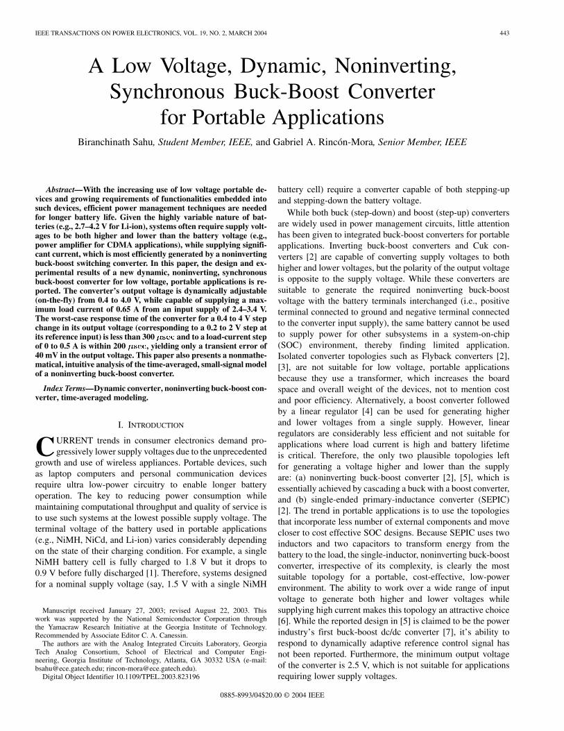
Fig. 1. Block diagram of a linear power amplifier system with dynamic supply.
An application where noninverting buck-boost convertersare in high demand is dynamically adaptive supplies forefficient, linear power amplifiers (PAs) in radio frequency(RF) transceivers used for communicating with base stations inportable wireless devices [8]. To prolong battery life, the powerefficiency of the PA is improved by dynamically changing thesupply voltage and current, on-demand. An efficient linear PAscheme with a dynamic buck-boost converter supply voltageis shown in Fig. 1. The buck-boost converter, dependingon a reference control signal adjusts the supply voltage tothe PA. To implement closed-loop power control in moderncommunication systems [9], based on its distance from thebase station, the transmitter adjusts the strength of the RFsignal at the antenna. Since the gain of the PA is constantfor the entire output power range, depending on the input RFpower, which is also representative of the power handled bythe PA, the reference control signal of the buck-boost converteris generated—a detailed description of this scheme is foundin [8]. Since the transmitted power is adjusted in real time,a dynamically adaptive buck-boost converter is required, thedesign and implementation of which is the subject of this paper.Other applications, such as MPEG-4 codecs [10] and dynamicvoltage scaling (DVS) processors [11] require variable supplyvoltages, depending on the workload, to enable longer batteryoperation in portable devices.
The paper is organized as follows. The single-inductor, non-inverting synchronous buck-boost converter is discussed andits key waveforms are presented in Section II. In Section III,an intuitive, nonmathematical explanation of the time-averagedsmall-signal model of the power stage of the buck-boostconverter is discussed. Analysis for different loading conditionsand design considerations, including stability and frequencycompensation, of a voltage-mode buck-boost converter arepresented. Analytical expressions for critical power loss mech-anisms in the converter are highlighted. Section IV describesthe details of the hardware design and implementation of theexperimental prototype converter. In Section V, results of theprototype converter and discussions are offered. Finally, thepaper is concluded in Section VI.
II. BACKGROUND
A noninverting buck-boost converter is essentially a cas-cade combination of a buck converter followed by a boostconverter, where a single inductor-capacitor is used for both[2], [6]. For low voltage implementations, the efficiency ofthe converter is improved by replacing the rectifier diodeswith switches, which results in a synchronous converter
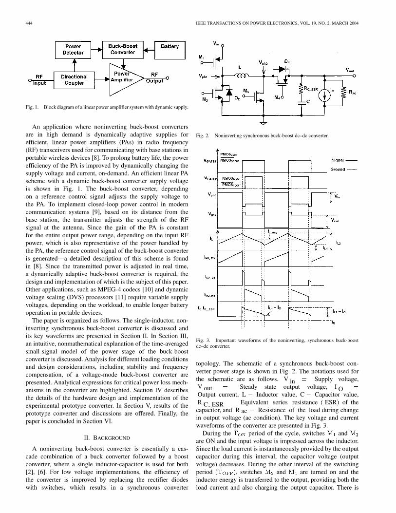
Fig. 2. Noninverting synchronous buck-boost dc–dc converter.
Fig. 3. Important waveforms of the noninverting, synchronous buck-boostdc–dc converter.
topology. The schematic of a synchronous buck-boost con-verter power stage is shown in Fig. 2. The notations used forthe schematic are as follows. V in Supply voltage,V out Steady state output voltage, I OOutput current, L Inductor value, C Capacitor value,R C ESR Equivalent series resistance ESR of thecapacitor, and R ac Resistance of the load during changein output voltage (ac condition). The key voltage and currentwaveforms of the converter are presented in Fig. 3.
During the period of the cycle, switches andare ON and the input voltage is impressed across the inductor.Since the load current is instantaneously provided by the outputcapacitor during this interval, the capacitor voltage (outputvoltage) decreases. During the other interval of the switchingperiod , switches and are turned on and theinductor energy is transferred to the output, providing both theload current and also charging the output capacitor. There is
SAHU AND RINCÓN-MORA: LOW VOLTAGE, DYNAMIC, NONINVERTING, SYNCHRONOUS BUCK-BOOST CONVERTER 445
a time delay (known as dead-time) between turning off ,and turning on , to prevent shoot-through current.
During this period, the inductor current flows through bodydiodes and , from transistors and , respectively.The duty cycle (D) of the converter is given by
(1)
where T is the switching time period of the converter.Since the node is connected to for DT time over a
period of T, the average voltage . Similarly,the average node voltage of can be given by
. Under steady-state operating condition,the inductor can be treated as short, and the average voltage of
and are equal
(2)
For the duty cycle of 0.5, the output voltage is equal to the inputvoltage. When duty cycle is less than 0.5, the output voltage islower than the input (buck mode), and for duty cycle greater than0.5, the output voltage is higher than the input (boost mode).
For low output voltages below the threshold voltage ofthe PMOS ( in the schematic), the transistor never turnsON, leaving only the diode as the switch resulting inasynchronous operation of the converter, which is inefficientbecause of the large voltage drop across the body diode. Atransmission gate, which is a parallel combination of a PMOSand a NMOS with complimentary logic inputs to their gates,can be used in place of PMOS boost transistor to operatethe converter in synchronous mode. For output voltages belowthe threshold voltage of PMOS, the NMOS acts as switch, andfor higher output voltages, NMOS turns-off while PMOS actas a switch. For intermediate output voltages, both PMOS andNMOS of the transmission gate remain ON to share the currentduring the switching interval in which the inductor is connectedto the output.
III. SYSTEM DESIGN CONSIDERATIONS
A. Time-Averaged Small-Signal Model Intuitive Explanation
Feedback control system is employed in dc–dc converters toregulate the output voltage, regardless of the changes in inputvoltage or loading conditions. To design the feedback controlloop of dc–dc switching regulators, an equivalent small-signalmodel of the power stage is required that is valid for low fre-quency perturbation of the duty cycle. To model the power stageof converters, techniques such as state-space averaging and cir-cuit averaging [2], [12] have been used extensively. However,the derivation is mathematically complex and difficult to relateto intuitive operation. In this section, a time-averaged model fora synchronous buck-boost converter power stage is explainedintuitively with precise one-to-one mapping with the operationof the circuit.
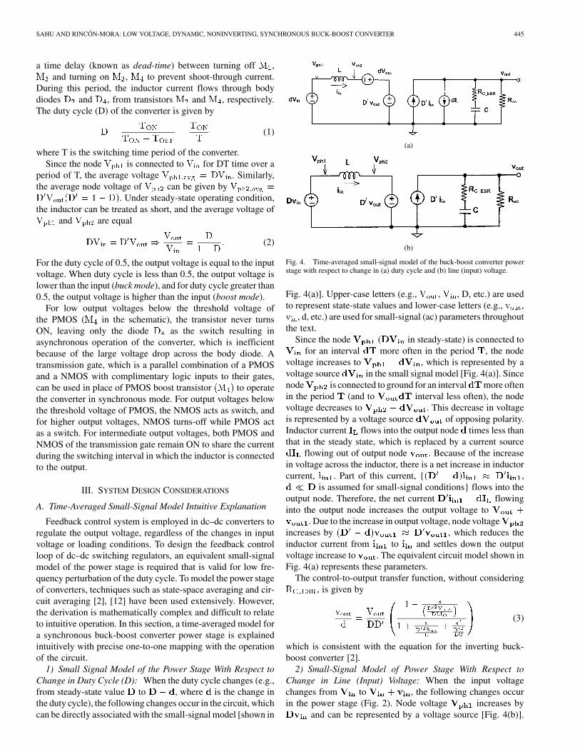
1) Small Signal Model of the Power Stage With Respect toChange in Duty Cycle (D): When the duty cycle changes (e.g.,from steady-state value to , where is the change inthe duty cycle), the following changes occur in the circuit, whichcan be directly associated with the small-signal model [shown in
(a)
(b)
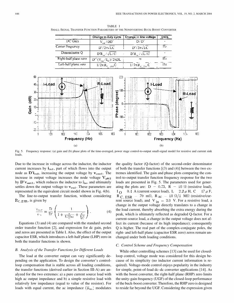
Fig. 4. Time-averaged small-signal model of the buck-boost converter powerstage with respect to change in (a) duty cycle and (b) line (input) voltage.
Fig. 4(a)]. Upper-case letters (e.g., , , D, etc.) are usedto represent state-state values and lower-case letters (e.g., ,
, d, etc.) are used for small-signal (ac) parameters throughoutthe text.
Since the node ( in steady-state) is connected tofor an interval more often in the period , the node
voltage increases to , which is represented by avoltage source in the small signal model [Fig. 4(a)]. Sincenode is connected to ground for an interval more oftenin the period (and to interval less often), the nodevoltage decreases to . This decrease in voltageis represented by a voltage source of opposing polarity.Inductor current flows into the output node times less thanthat in the steady state, which is replaced by a current source
flowing out of output node . Because of the increasein voltage across the inductor, there is a net increase in inductorcurrent, . Part of this current, { ,
is assumed for small-signal conditions} flows into theoutput node. Therefore, the net current flowinginto the output node increases the output voltage to
. Due to the increase in output voltage, node voltageincreases by , which reduces theinductor current from to and settles down the outputvoltage increase to . The equivalent circuit model shown inFig. 4(a) represents these parameters.
The control-to-output transfer function, without considering, is given by
(3)
which is consistent with the equation for the inverting buck-boost converter [2].
2) Small-Signal Model of Power Stage With Respect toChange in Line (Input) Voltage: When the input voltagechanges from to , the following changes occurin the power stage (Fig. 2). Node voltage increases by
and can be represented by a voltage source [Fig. 4(b)].
446 IEEE TRANSACTIONS ON POWER ELECTRONICS, VOL. 19, NO. 2, MARCH 2004
TABLE ISMALL-SIGNAL TRANSFER FUNCTION PARAMETERS OF THE NONINVERTING BUCK-BOOST CONVERTER
(a) (b)
Fig. 5. Frequency response: (a) gain and (b) phase plots of the time-averaged, power stage control-to-output small-signal model for resistive and current sinkloads.
Due to the increase in voltage across the inductor, the inductorcurrent increases by , part of which flows into the outputnode as , increasing the output voltage by . Theincrease in output voltage increases the node voltageby , which reduces the inductor to , and ultimatelysettles down the output voltage to . These parameters arerepresented in the equivalent circuit model shown in Fig. 4(b).
The line-to-output transfer function, without considering, is given by
(4)
Equations (3) and (4) are compared with the standard secondorder transfer function [2], and expression for dc gain, polesand zeros are presented in Table I. Also, the effect of the outputcapacitor ESR, which introduces a left-half plane (LHP) zero inboth the transfer functions is shown.
B. Analysis of the Transfer Functions for Different Loads
The load at the converter output can vary significantly de-pending on the application. To design the converter’s control-loop compensation that is stable across all loading conditions,the transfer functions (derived earlier in Section III-A) are an-alyzed for the two extremes: a) a pure current source load withhigh ac output impedance and b) a simple resistive load withrelatively low impedance (equal to value of the resistor). Forloads with equal current, the ac impedance modulates
the quality factor (Q-factor) of the second-order denominatorof both the transfer functions [(3) and (4)] between the two ex-tremes identified. The gain and phase plots comparing the con-trol-to-output transfer function frequency response for the twoloads are presented in Fig. 5. The parameters used for gener-ating the plots are: D , R (resistive load),I O A (current source load), L H, C F,R C ESR m , R ac M (resistive/cur-rent source load), and V in V. For a resistive load, achange in the output voltage directly translates to a change inthe load current, thereby absorbing the extra energy during thepeak, which is ultimately reflected as degraded Q-factor. For acurrent-source load, a change in the output voltage does not af-fect its current (because of its high impedance); consequentlyQ is higher. The real part of the complex-conjugate poles, theright- and left-half plane (capacitor ESR zero) zeros remain un-changed under both loading conditions.
C. Control Scheme and Frequency Compensation
While other controlling schemes [13] can be used for closed-loop control, voltage mode was considered for this design be-cause of its simplicity (no inductor current information is re-quired). Voltage-mode control enjoys popularity in the industryfor simple, point-of-load dc–dc converter applications [14]. Aswith the boost converter, the right-half plane (RHP) zero limitsthe unity-gain frequency (UGF) of the closed-loop performanceof the buck-boost converter. Therefore, the RHP zero is designedto reside far beyond the UGF. Considering the expression given
SAHU AND RINCÓN-MORA: LOW VOLTAGE, DYNAMIC, NONINVERTING, SYNCHRONOUS BUCK-BOOST CONVERTER 447
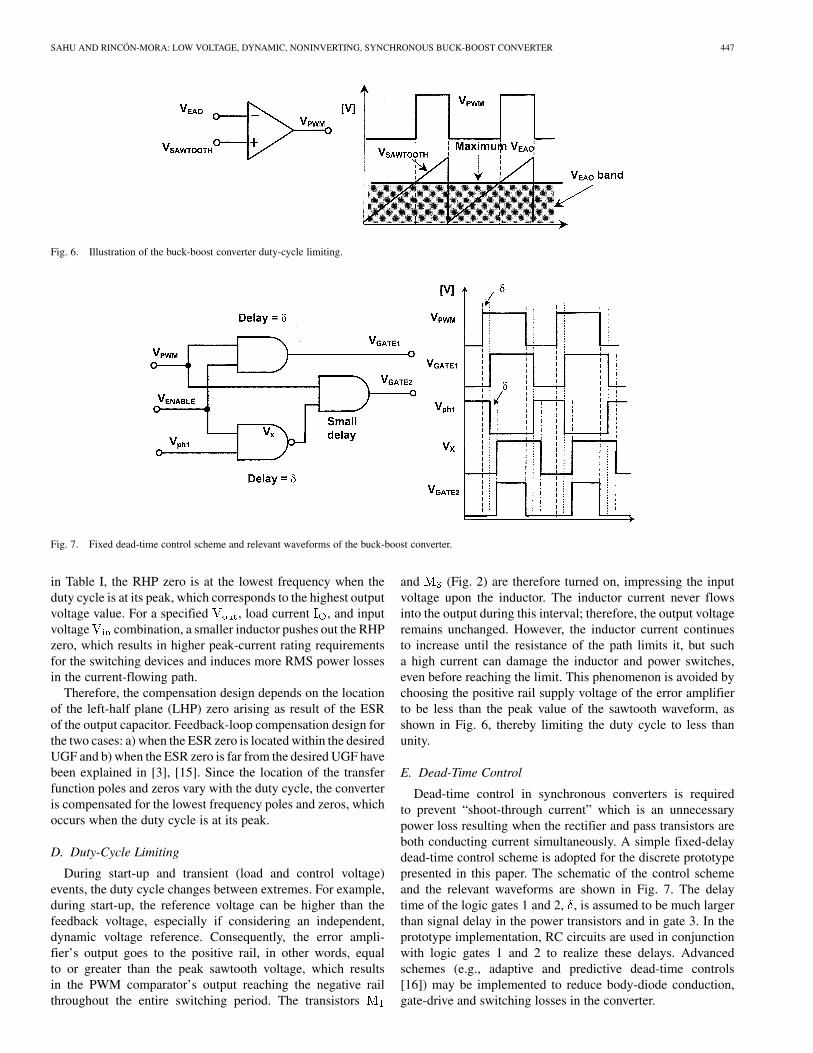
Fig. 6. Illustration of the buck-boost converter duty-cycle limiting.
Fig. 7. Fixed dead-time control scheme and relevant waveforms of the buck-boost converter.
in Table I, the RHP zero is at the lowest frequency when theduty cycle is at its peak, which corresponds to the highest outputvoltage value. For a specified , load current , and inputvoltage combination, a smaller inductor pushes out the RHPzero, which results in higher peak-current rating requirementsfor the switching devices and induces more RMS power lossesin the current-flowing path.
Therefore, the compensation design depends on the locationof the left-half plane (LHP) zero arising as result of the ESRof the output capacitor. Feedback-loop compensation design forthe two cases: a) when the ESR zero is located within the desiredUGF and b) when the ESR zero is far from the desired UGF havebeen explained in [3], [15]. Since the location of the transferfunction poles and zeros vary with the duty cycle, the converteris compensated for the lowest frequency poles and zeros, whichoccurs when the duty cycle is at its peak.
D. Duty-Cycle Limiting
During start-up and transient (load and control voltage)events, the duty cycle changes between extremes. For example,during start-up, the reference voltage can be higher than thefeedback voltage, especially if considering an independent,dynamic voltage reference. Consequently, the error ampli-fier’s output goes to the positive rail, in other words, equalto or greater than the peak sawtooth voltage, which resultsin the PWM comparator’s output reaching the negative railthroughout the entire switching period. The transistors
and (Fig. 2) are therefore turned on, impressing the inputvoltage upon the inductor. The inductor current never flowsinto the output during this interval; therefore, the output voltageremains unchanged. However, the inductor current continuesto increase until the resistance of the path limits it, but sucha high current can damage the inductor and power switches,even before reaching the limit. This phenomenon is avoided bychoosing the positive rail supply voltage of the error amplifierto be less than the peak value of the sawtooth waveform, asshown in Fig. 6, thereby limiting the duty cycle to less thanunity.
E. Dead-Time Control
Dead-time control in synchronous converters is requiredto prevent “shoot-through current” which is an unnecessarypower loss resulting when the rectifier and pass transistors areboth conducting current simultaneously. A simple fixed-delaydead-time control scheme is adopted for the discrete prototypepresented in this paper. The schematic of the control schemeand the relevant waveforms are shown in Fig. 7. The delaytime of the logic gates 1 and 2, , is assumed to be much largerthan signal delay in the power transistors and in gate 3. In theprototype implementation, RC circuits are used in conjunctionwith logic gates 1 and 2 to realize these delays. Advancedschemes (e.g., adaptive and predictive dead-time controls[16]) may be implemented to reduce body-diode conduction,gate-drive and switching losses in the converter.
448 IEEE TRANSACTIONS ON POWER ELECTRONICS, VOL. 19, NO. 2, MARCH 2004
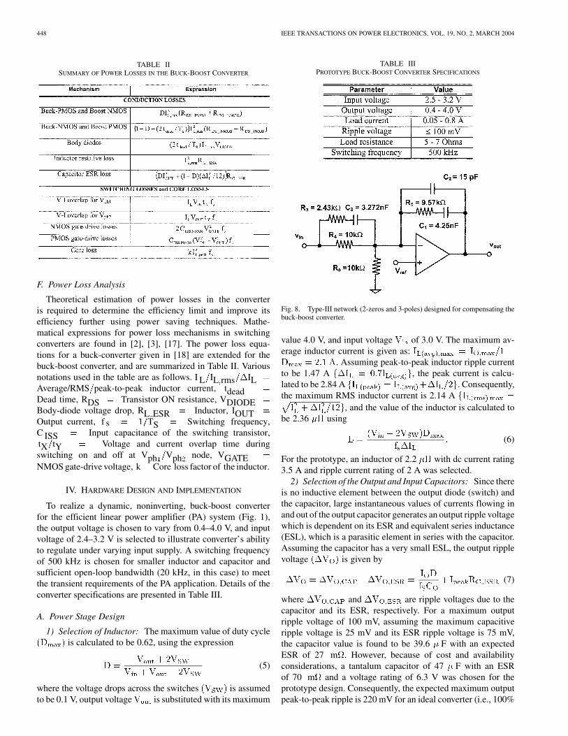
TABLE IISUMMARY OF POWER LOSSES IN THE BUCK-BOOST CONVERTER
F. Power Loss Analysis
Theoretical estimation of power losses in the converteris required to determine the efficiency limit and improve itsefficiency further using power saving techniques. Mathe-matical expressions for power loss mechanisms in switchingconverters are found in [2], [3], [17]. The power loss equa-tions for a buck-converter given in [18] are extended for thebuck-boost converter, and are summarized in Table II. Variousnotations used in the table are as follows. I L IL rms ILAverage/RMS peak-to-peak inductor current, tdeadDead time, RDS Transistor ON resistance, VDIODEBody-diode voltage drop, RL ESR Inductor, IOUTOutput current, f s TS Switching frequency,C ISS Input capacitance of the switching transistor,tX tY Voltage and current overlap time duringswitching on and off at Vph Vph node, VGATENMOS gate-drive voltage, k Core loss factor of the inductor.
IV. HARDWARE DESIGN AND IMPLEMENTATION
To realize a dynamic, noninverting, buck-boost converterfor the efficient linear power amplifier (PA) system (Fig. 1),the output voltage is chosen to vary from 0.4–4.0 V, and inputvoltage of 2.4–3.2 V is selected to illustrate converter’s abilityto regulate under varying input supply. A switching frequencyof 500 kHz is chosen for smaller inductor and capacitor andsufficient open-loop bandwidth (20 kHz, in this case) to meetthe transient requirements of the PA application. Details of theconverter specifications are presented in Table III.
A. Power Stage Design
1) Selection of Inductor: The maximum value of duty cycleis calculated to be 0.62, using the expression
(5)
where the voltage drops across the switches is assumedto be 0.1 V, output voltage is substituted with its maximum
TABLE IIIPROTOTYPE BUCK-BOOST CONVERTER SPECIFICATIONS
Fig. 8. Type-III network (2-zeros and 3-poles) designed for compensating thebuck-boost converter.
value 4.0 V, and input voltage of 3.0 V. The maximum av-erage inductor current is given as:
. Assuming peak-to-peak inductor ripple currentto be 1.47 A , the peak current is calcu-lated to be 2.84 A . Consequently,the maximum RMS inductor current is 2.14 A
, and the value of the inductor is calculated tobe 2.36 using
(6)
For the prototype, an inductor of 2.2 with dc current rating3.5 A and ripple current rating of 2 A was selected.
2) Selection of the Output and Input Capacitors: Since thereis no inductive element between the output diode (switch) andthe capacitor, large instantaneous values of currents flowing inand out of the output capacitor generates an output ripple voltagewhich is dependent on its ESR and equivalent series inductance(ESL), which is a parasitic element in series with the capacitor.Assuming the capacitor has a very small ESL, the output ripplevoltage is given by
(7)
where and are ripple voltages due to thecapacitor and its ESR, respectively. For a maximum outputripple voltage of 100 mV, assuming the maximum capacitiveripple voltage is 25 mV and its ESR ripple voltage is 75 mV,the capacitor value is found to be 39.6 F with an expectedESR of 27 m . However, because of cost and availabilityconsiderations, a tantalum capacitor of 47 F with an ESRof 70 m and a voltage rating of 6.3 V was chosen for theprototype design. Consequently, the expected maximum outputpeak-to-peak ripple is 220 mV for an ideal converter (i.e., 100%
SAHU AND RINCÓN-MORA: LOW VOLTAGE, DYNAMIC, NONINVERTING, SYNCHRONOUS BUCK-BOOST CONVERTER 449
(a) (b)
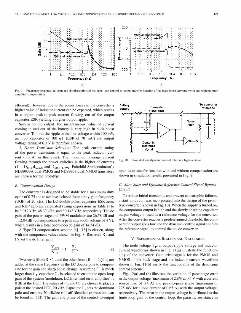
Fig. 9. Frequency response: (a) gain and (b) phase plots of the open-loop control-to-output transfer function of the buck-boost converter with and without erroramplifier compensation.
efficient). However, due to the power losses in the converter ahigher value of inductor current can be expected, which resultsin a higher peak-to-peak current flowing out of the outputcapacitor ESR yielding a higher output ripple.
Similar to the output, the instantaneous value of currentcoming in and out of the battery is very high in buck-boostconverter. To limit the ripple in the line voltage within 100 mV,an input capacitor of 100 F (ESR of 70 m ) and outputvoltage rating of 6.3 V is therefore chosen.
3) Power Transistor Selection: The peak current ratingof the power transistors is equal to the peak inductor cur-rent (3.0 A, in this case). The maximum average currentflowing through the power switches is the higher of currents
and . Fairchild Semiconductor’sNDS9933A dual-PMOS and NDS9958 dual-NMOS transistorsare chosen for the prototype.
B. Compensation Design
The converter is designed to be stable for a maximum dutycycle of 0.75 and to achieve a closed-loop, unity-gain frequency(UGF) of 20 kHz. The LC-double poles, capacitor-ESR zero,and RHP zero are calculated (using expressions in Table I) tobe 3.912 kHz, 48.37 kHz, and 30.143 kHz, respectively. The dcgain of the power stage and PWM modulator are 26.58 dB and
12.04 dB (corresponding to a peak saw tooth voltage of 4 V),which results in a total open-loop dc gain of 14.54 dB.
A Type-III compensation scheme [4], [15] is chosen, alongwith the component values shown in Fig. 8. Resistors and
set the dc filter gain
(8)
Two zeros [from , and the other from ] areadded at the same frequency as the LC double pole to compen-sate for the gain and sharp phase change. Assuming is muchlarger than , capacitor is selected to ensure the open-loopgain of the system (modulator, LC filter, and error amplifier) is0 dB at the UGF. The values of and are chosen to place apole at the desired UGF, 20 kHz. Capacitor sets the dominantpole and ensures 20 dB/dec roll-off (detailed expressions canbe found in [15]). The gain and phase of the control-to-output
Fig. 10. Slow start and dynamic control reference bypass circuit.
open-loop transfer function with and without compensation areshown in simulation results presented in Fig. 9.
C. Slow-Start and Dynamic Reference Control Signal BypassCircuit
To reduce initial transients, and prevent catastrophic failures,a start-up circuit was incorporated into the design of the proto-type converter (shown in Fig. 10). When the supply is turned on,the comparator output is high and the slowly charging capacitoroutput voltage is used as a reference voltage for the converter.After the converter reaches a predetermined threshold, the com-parator output goes low and the dynamic control signal enablesthe reference signal to control the dc–dc converter.
V. EXPERIMENTAL RESULTS AND DISCUSSIONS
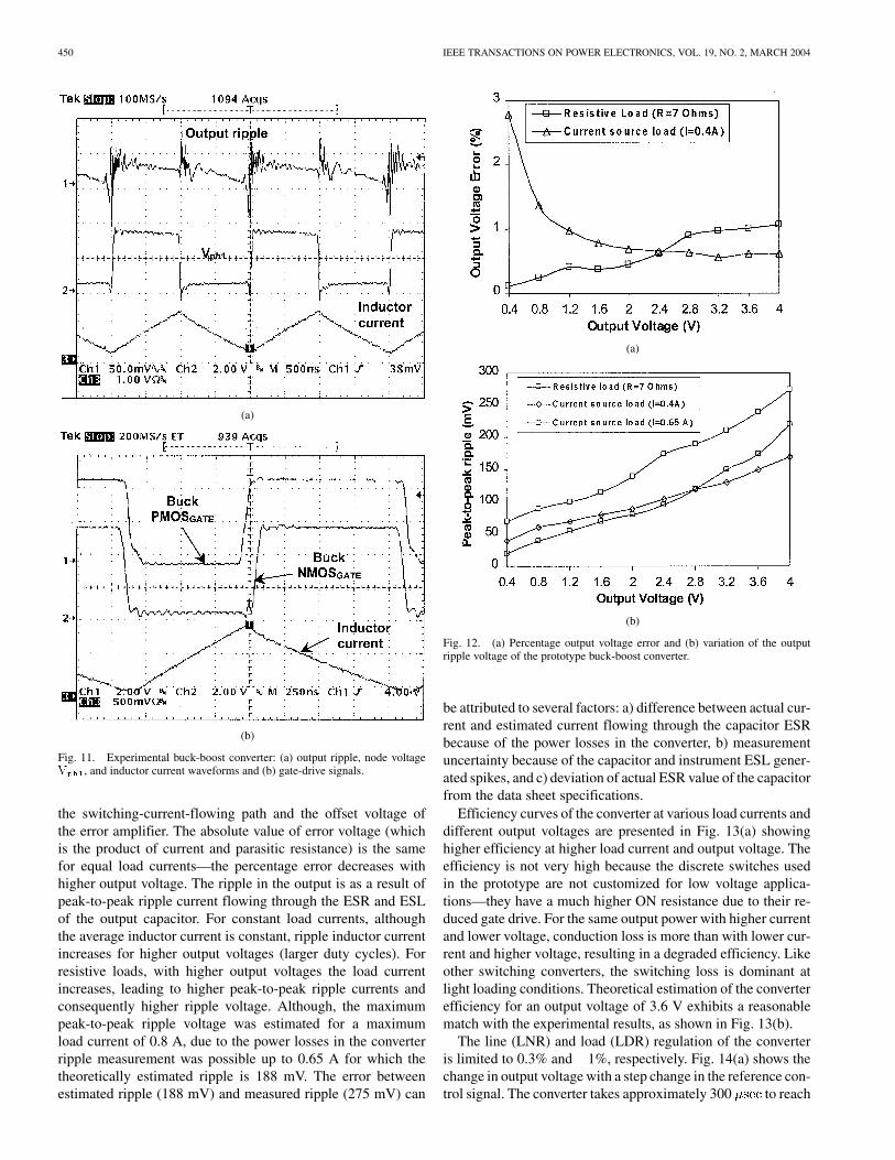
The node voltage , output ripple voltage and inductorcurrent waveforms shown in Fig. 11(a) illustrate the function-ality of the converter. Gate-drive signals for the PMOS andNMOS of the buck stage and the inductor current waveformshown in Fig. 11(b) verify the functionality of the dead-timecontrol scheme.
Fig. 12(a) and (b) illustrate the variation of percentage errorin the output voltage (maximum of 2.8% at 0.4 V with a currentsource load of 0.4 A) and peak-to-peak ripple (maximum of275 mV for a load current of 0.65 A) with the output voltage,respectively. The error in the output voltage is attributed to thefinite loop gain of the control loop, the parasitic resistance in
450 IEEE TRANSACTIONS ON POWER ELECTRONICS, VOL. 19, NO. 2, MARCH 2004
(a)
(b)
Fig. 11. Experimental buck-boost converter: (a) output ripple, node voltageV , and inductor current waveforms and (b) gate-drive signals.
the switching-current-flowing path and the offset voltage ofthe error amplifier. The absolute value of error voltage (whichis the product of current and parasitic resistance) is the samefor equal load currents—the percentage error decreases withhigher output voltage. The ripple in the output is as a result ofpeak-to-peak ripple current flowing through the ESR and ESLof the output capacitor. For constant load currents, althoughthe average inductor current is constant, ripple inductor currentincreases for higher output voltages (larger duty cycles). Forresistive loads, with higher output voltages the load currentincreases, leading to higher peak-to-peak ripple currents andconsequently higher ripple voltage. Although, the maximumpeak-to-peak ripple voltage was estimated for a maximumload current of 0.8 A, due to the power losses in the converterripple measurement was possible up to 0.65 A for which thetheoretically estimated ripple is 188 mV. The error betweenestimated ripple (188 mV) and measured ripple (275 mV) can
(a)
(b)
Fig. 12. (a) Percentage output voltage error and (b) variation of the outputripple voltage of the prototype buck-boost converter.
be attributed to several factors: a) difference between actual cur-rent and estimated current flowing through the capacitor ESRbecause of the power losses in the converter, b) measurementuncertainty because of the capacitor and instrument ESL gener-ated spikes, and c) deviation of actual ESR value of the capacitorfrom the data sheet specifications.
Efficiency curves of the converter at various load currents anddifferent output voltages are presented in Fig. 13(a) showinghigher efficiency at higher load current and output voltage. Theefficiency is not very high because the discrete switches usedin the prototype are not customized for low voltage applica-tions—they have a much higher ON resistance due to their re-duced gate drive. For the same output power with higher currentand lower voltage, conduction loss is more than with lower cur-rent and higher voltage, resulting in a degraded efficiency. Likeother switching converters, the switching loss is dominant atlight loading conditions. Theoretical estimation of the converterefficiency for an output voltage of 3.6 V exhibits a reasonablematch with the experimental results, as shown in Fig. 13(b).
The line (LNR) and load (LDR) regulation of the converteris limited to 0.3% and 1%, respectively. Fig. 14(a) shows thechange in output voltage with a step change in the reference con-trol signal. The converter takes approximately 300 to reach
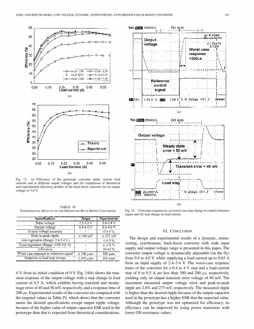
SAHU AND RINCÓN-MORA: LOW VOLTAGE, DYNAMIC, NONINVERTING, SYNCHRONOUS BUCK-BOOST CONVERTER 451
(a)
(b)
Fig. 13. (a) Efficiency of the prototype converter under various loadcurrents and at different output voltages and (b) comparison of theoreticaland experimental efficiency profiles of the buck-boost converter for an outputvoltage of 3.6 V.
TABLE IVEXPERIMENTAL RESULTS OF THE PROTOTYPE BUCK-BOOST CONVERTER
4 V, from its initial condition of 0 V. Fig. 14(b) shows the tran-sient response of the output voltage with a step change in loadcurrent of 0.5 A, which exhibits having transient and steady-stage error of 40 and 50 mV, respectively, and a response time of200 . Experimental results of the converter are compared withthe targeted values in Table IV, which shows that the convertermeets the desired specifications except output ripple voltage,because of the higher value of output capacitor ESR used in theprototype than that is expected from theoretical considerations.
(a)
(b)
Fig. 14. Converter response to: (a) worst-case step change in control referencesignal and (b) step change in load current.
VI. CONCLUSION
The design and experimental results of a dynamic, nonin-verting, synchronous, buck-boost converter with wide inputsupply and output voltage range is presented in this paper. Theconverter output voltage is dynamically adjustable (on the fly)from 0.4 to 4.0 V, while supplying a load current up to 0.65 Afrom an input supply of 2.4–3.4 V. The worst-case responsetimes of the converter for a 0.4 to 4 V step and a load-currentstep of 0 to 0.5 A are less than 300 and 200 , respectively,yielding only an output transient error voltage of 40 mV. Themaximum measured output voltage error and peak-to-peakripple are 2.8% and 275 mV, respectively. The measured rippleis higher than the desired ripple because of the output capacitorused in the prototype has a higher ESR that the expected value.Although the prototype was not optimized for efficiency, itsefficiency can be improved by using power transistors withlower ON-resistance values.

452 IEEE TRANSACTIONS ON POWER ELECTRONICS, VOL. 19, NO. 2, MARCH 2004
An intuitive derivation of the time-averaged model of thepower stage of the converter is also discussed, which reveals thecharacteristics of the system under extreme, worst-case loadingconditions from pure current source to a pure resistive load. Apure current source load (infinite output impedance) shows ahigher Q at the resonant LC poles frequency. Overall, with theincreasing use of battery-operated portable devices, to run thesystems at their peak performance levels (even when the batteryis close to fully discharged), noninverting buck-boost convertersplay a pivotal role in the next generation power management cir-cuits, especially as it pertains to SOC implementations.
REFERENCES
[1] C. Simpson. (2003) Characteristics of Rechargeable Batteries. Na-tional.com. [Online]. Available: http://www.national.com/appinfo/power/files/fv.pdf.
[2] R. W. Erickson, Fundamentals of Power Electronics, 1st ed. NewYork: Chapman and Hall, 1997.
[3] A. Pressman, Switching Power Supply Design, 2nd ed. New York: Mc-Graw-Hill, 1998.
[4] (2003) Maxim Semiconductors’ Application Note. [Online] http://www.maxim-ic.com/appnotes.cfm/appnote_number/312
[5] “Design Applications Notes,” Tech. Rep., Linear Technology, Oct. 2001.[6] R. Lenk, Practical Design of Power Supplies. New York: McGraw-
Hill, 1998.[7] LTC3440: The power industries first buck-boost dc/dc converter. Tech.
Rep., Linear Technology. [Online]. Available: http://www.soanar.com.au/newsandinfo.cfm?newsid=232&archive=1
[8] B. Sahu and G. A. Rincón-Mora, “A high-efficiency, linear RF poweramplifier with a power-tracking, dynamically adaptive buck-boostsupply,” IEEE Trans. Microwave Theory Tech., to be published.
[9] S. C. Yang, CDMA RF Systems Engineering. Norwood, MA: ArtechHouse, 1999.
[10] F. Ichiba, K. Suzuki, S. Mita, T. Kuroda, and T. Furuyama, “Variablesupply-voltage scheme with 95% efficiency DC-DC converter forMPEG-4 codec,” in Proc. Int. Symp. Low Power Electron., 1999, pp.54–59.
[11] A. Sinha and A. Chandrakasan, “Dynamic power management in wire-less sensor networks,” IEEE Design Test Comput., vol. 18, pp. 62–74,Mar./Apr. 2001.
[12] Y. Lee, Computer-Aided Analysis and Design of Switch-Mode PowerSupplies. New York: Mercel-Dekker, Inc., 1993.
[13] G. A. Rincón-Mora, “Self-oscillating hysteretic V-mode DC-DC con-trollers: from the ground up,” in Proc. IEEE Power Electron. Spec. Conf.(PESC) Tutorial, 2001.
[14] B. Shaffer, “Internal compensation—Boon or Bane,” in Proc. PowerSupply Design Sem. (SEM 1300), 2000.
[15] Texas Instruments, “Designing With the TL5001 PWM Controller,” Ap-plicat. Rep. SLVA034A, Texas Instruments, 1995.
[16] B. Lynch and K. Hesse, “Under the hood of low-voltage dc/dc con-verters,” in Proc. Power Supply Design Seminar (SEM 1500), 2002.
[17] L. Balogh, “Design and application guide for high speed MOSFET gatedrive circuits,” in Proc. Power Supply Design Seminar (SEM 1400),2001.
[18] G. A. Rincón-Mora, “Integrated dc–dc converters: a topologicaljourney,” in Proc. Midwest Symp. Circuits Syst (MWCAS’02) Tutorial,2002.
Biranchinath Sahu (S’01) was born in Nodhana,Orissa, India. He received the B.E. degree (withhighest honors) from the University College of Engi-neering, Burla, India, in 1997 and the M.Tech. degreefrom the Indian Institute of Technology, Kanpur,India, in 1999, both in electrical engineering, andis currently pursuing the Ph.D. degree in the Schoolof Electrical and Computer Engineering, GeorgiaInstitute of Technology, Atlanta.
His research interests are in the area of mixed-signal circuits and system design, more specifically,
integrated power management, and design of energy-efficient, linear RF poweramplifiers for battery-powered, portable applications. During Summer 2001, hewas an Intern at Analog Devices, Inc., Wilmington, MA, working on the de-sign and simulation of delta-sigma converters for GSM wireless applications.He was a full-time member of the Microelectronics Group, Lucent Technolo-gies, Inc. (now Agere Systems, Inc.), India, in 2000, where he had worked onthe development of reduced-order modeling and simulation tools for high-speedinterconnects and RF circuits.
Gabriel A. Rincón-Mora (S’91–M’97–SM’01)was born in Caracas, Venezuela. He received theB.S.E.E. degree (with high honors) from FloridaInternational University, Miami, in 1992 and theM.S.E.E. and Ph.D. degrees in electrical engineeringfrom the Georgia Institute of Technology (GeorgiaTech), Atlanta, in 1994 and 1996, respectively.
In 1994, he started working with Texas Instru-ments as a Design Engineer, eventually becominga Senior IC Designer, Design Team Leader, andMember of Group Technical Staff. In 1999, he
was appointed Adjunct Professor for the School of Electrical and ComputerEngineering, Georgia Tech. He is presently a full-time member of the facultyat Georgia Tech and the Director of the Georgia Tech Analog Consortium.His research is on analog and mixed-signal integrated circuit design and,more specifically, on low voltage, low power consumption, low/high outputpower, high efficiency, system-on-chip solutions for power management andother analog system applications, in portable battery-powered and nonportableelectronic equipment. His work has focused on the research, design, anddevelopment of device physics, circuits, and systems, in different flavors ofBipolar, CMOS, and BiCMOS process technologies. He has numerous patentsas well as publications in the field. He also teaches short courses, seminar, andtutorial on the subject of integrated power management. He authored VoltageReferences: From Diodes to Precision High-Order Bandgap Circuits (NewYork: Wiley, 2001).
Dr. Rincón-Mora received the “National Hispanic in Technology Award”from the Society of Professional Hispanic Engineers, was inducted into the“Council of Outstanding Young Engineering Alumni” by Georgia Tech,received the “Charles E. Perry Visionary Award” from Florida InternationalUniversity, received a “Commendation Certificate” from the LieutenantGovernor of California, and is listed in Marquis’ Who’s Who in America. Heis a member of Tau Beta Pi, Eta Kappa Nu, Phi Kappa Phi, and the Society ofHispanic Professional Engineers.