switched-capacitor bandpass delta-sigma a/d …€¦ · page 1 of 27 switched-capacitor bandpass...
TRANSCRIPT
Switched-Capacitor Bandpass Delta-Sigma A/D Modulation at 10.7MHz
Frank W. Singor and W. Martin Snelgrove*
Department of Electrical and Computer Engineering, University of Toronto, Toronto, Canada M5S 1A4* Department of Electronics, Carleton University, Ottawa, Canada K1S 5B6
ABSTRACT
Two second-order bandpass delta-sigma A/D modulators have been implemented in a BiC-
MOS process [1] to demonstrate the feasibility of converting a 10.7 MHz radio IF signal to digital
form. The circuits, based on switched-capacitor biquads, demonstrated 57dB SNR in a 200 kHz
bandwidth when clocked at , dissipating 60mW from a 5V supply.
I. INTRODUCTION
There is broad industrial interest in A/D conversion at the intermediate-frequency (IF) stage of a
radio, because that allows digital channel-select filtering, gain control and demodulation. The
robustness of the digital circuitry gives manufacturing advantages and allows the use of sophisti-
cated algorithms, which are especially useful with digitally coded transmissions and where multi-
ple transmission standards are in use. Because this is a new application area for A/D conversion
the system-level trade-offs needed to specify the converters are still a matter of debate. This work
contributes by demonstrating experimentally that it is feasible to make a fully monolithic con-
verter with the bandwidth required for a per-channel GSM radio or several channels of IS-54 [2]
and enough dynamic range to simplify gain-control and adjacent-channel rejection. It also sug-
gests a preferred clocking scheme for high speeds.
We extrapolate from the experimental part to suggest that it is practical to build a converter able to
cover an entire band for narrowband personal communications basestations or the
that covers all of the North American cellular standards from IS-95 to AMPS, and with
enough dynamic range to do all channel selection and gain control functions on the digital side.
For telephony there are two distinct variants of the radio design problem — one for base stations
and the other for the terminals. For example, the base station is expected to handle several chan-
nels, while the terminal generally operates only on a single channel; on the other hand power con-
straints are tighter in the terminal. The converter we demonstrate is aimed at a single channel of
GSM telephony and has low enough power for a terminal, and the wider-band converters we
extrapolate to are intended for base stations.
The A/D conversion required can be done at baseband on quadrature channels (using a “zero-IF”
receiver), but (for the multi-channel problem) that requires precision matching and (for both base
0.8µ
42.8MHz
1MHz
1.25MHz
Page 1 of 27
stations and terminals) is susceptible to a variety of DC instabilities and electromagnetic compati-
bility problems. Alternately a bandpass signal can be directly converted either with a conventional
or noise-shaped converter. Noise-shaped (or ) converters, which we demonstrate here, consist
of a filter and comparator in a feedback loop as in Fig. 1, and are oversampled. (that is, sampled
well above the Nyquist rate for the bandwidth required). The type of filter used in the loop is a key
determinant of the performance possible.
II. PRIOR ART
Monolithic bandpass delta-sigma modulators have been reported [3][4][5] with centre frequencies
of 455kHz, 2MHz, and 50MHz, and with bandwidths of 10kHz, 30kHz and respectively
and resolutions of nine to fourteen bits. These bandwidths are suitable for broadcast and voice
AM, IS-54 cellular telephony and GSM telephony respectively. Another device obtained a
SNR performance with a centre frequency [6] and bandwidth using off-chip
inductors as resonators.
Using oversampling with wideband signals necessarily implies fast clocking, so there is a ques-
tion as to how wideband a monolithic realization can be. Brandt and Wooley showed that a 1MHz
bandwidth is possible in the lowpass case with a MASH architecture [7], and Song demonstrated
switched-capacitor (switched-C) bandpass filtering at 10.7MHz [8]. This work demonstrates in a
second-order modulator prototype that a 10.7MHz bandcentre is possible, with 57dB SNR perfor-
mance in a 200kHz band.
When channel-select filtering is to be performed after A/D conversion in a radio system it is of
prime importance to have high linearity, or else strong interferers may intermodulate in the con-
verter and mask the desired signal. This study focuses on switched-C technology because it is
proven for high resolution and linearity at baseband and because it is a monolithic technology
capable of delivering precision analog performance. Inductor- [6][9][10] or transconductor-based
[5] technologies can be expected to dominate at very high speeds, but are more difficult in that
they involve off-chip components or tuning; their linearity is also compromised by “intersymbol
interference” effects in the pulse feedback used as well as in the loop filter. Switched-C should be
expected to dominate up to some upper bandwidth limit, and this work helps estimate that limit.
This paper presents and compares (experimentally) two different types of second-order switched-
C bandpass modulators. The two structures both use fully differential BiCMOS op-amps with
continuous-time common-mode feedback, but employ different clock phasings to experiment
∆Σ
200kHz
55dB
6.5MHz 200kHz
∆Σ
Page 2 of 27
with trade-offs between active and passive sensitivities.
This paper is concerned with A/D modulation. To make a complete A/D converter decimation is
also required. Brandt and Wooley have recently shown that this can be done at low power for a
similar set of specifications: with 11.3MHz data and a 3V power supply they consumed only
6.5mW. [11] Extrapolating to our higher data rate suggests that 30mW should be sufficient.
II. MODULATOR DESIGN
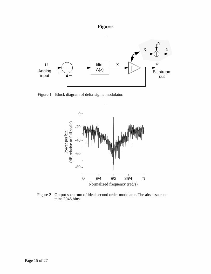
The basic one-bit modulator consists of a quantizer and a loop filter as shown in Fig. 1 [12]. Tra-
ditionally the filter block would just be an integrator resulting in a first-order lowpass modula-
tor. By choosing the loop filter [3][10][13] we can shape the noise away from any frequency band
desired. Modelling the quantizer by a linear white noise source, (shaded area in Fig. 1) we can
derive a noise transfer function and a signal transfer function . In terms of the loop-
filter gain 1 they are
...(eq.1)
and
...(eq.2)
and the overall output is a superposition of shaped noise and signal
...(eq.3)
For high-order filters or spectrally rich inputs the quantization noise is approximately white, [14]
so a deep notch in makes for a good signal-to-noise ratio in a narrow band.
For a simple second-order BP modulator with a centre frequency at one-quarter of the sam-
pling frequency
...(eq.4)
the filter response is given by giving noise gain
and signal gain . The output spectrum of the resulting ideal modulator with an
1. A quantizer also has a signal-dependent equivalent gain, which we have included in .
∆Σ
Hn z( ) Hu z( )
A z( )
A z( )
Hn z( ) 11 A z( )+-------------------=
Hu z( ) A z( )1 A z( )+-------------------=
Y Hn z( )N Hu z( )U+=
Hn
∆Σ
f o
f s
4-----=
A z( ) 1– z2
1+( )⁄= Hn z( ) z2
1+( ) z2⁄=
Hu z( ) 1 z2⁄–=
Page 3 of 27
input sine wave at midband is shown in Fig. 2. For the simulation a small random dither was
added to the input (in practical designs thermal noise is sometimes exploited to do this) to whiten
the quantizer noise and remove tones.
This particular loop filter, which is the one we implemented, has a precise mathematical relation-
ship to the well-understood first-order lowpass modulator: a change of variable [15]
...(eq.5)
gives
...(eq.6)
The mathematical properties of the first-order lowpass prototype delta-sigma converter using
are fairly well understood, including a simple stability guarantee and properties of the limit
cycles. These properties carry over to a bandpass version designed according to (eq. 5), with the
square term in the substitution giving the bandpass modulator the behaviour of two interleaved
first-order converters, each of them “highpass” because of the negative sign in (eq. 5).
This transformation gives our circuit the noise-shaping behaviour of a first-order lowpass con-
verter, with improvement in SNR for each octave of oversampling. It is also the one that
guarantees the stability of Longo’s fourth-order circuit [4] and gives it shaping.
FILTER STRUCTURE
There are many filter structures implementing a given , and with an ideal realization of the
filter all of them would give modulators with identical behaviour. In the presence of errors in
capacitor ratios and of finite gain and bandwidth in op-amps, though, they behave differently. The
most important effect is that the positions of the filter poles are affected in different ways by these
errors: if filter poles are at the wrong frequency (wrong angle, in the -plane) then the noise notch
(see Fig. 2) will not be properly centered, and if they move off the unit circle (wrong magnitude
of the complex pole, in the -plane) then the notch will be shallower. Fig. 3 plots effects of pole
position on overall SNR. It is also known that the effects of poles moving inside the unit circle are
subtly worse than those of moving slightly outside [16][17][18] because an “over-stable” filter
allows “deadbands” where limit cycles persist, and this can cause intermodulation distortion.
The “lossless discrete integrator” (LDI) loop of Fig. 4 has its poles at the zeros of , where
is the loop gain. The numerator of is , and the equal coefficients
∆Σ
z z2–=
A z( ) 1 z 1–( )⁄=
A z( )
9dB
15dB/octave
A z( )
z
z
1 L z( )–
L z( ) 1 L– z( ) z2 2 R+( )z– 1+
Page 4 of 27
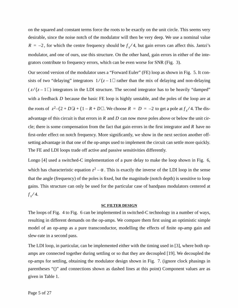
on the squared and constant terms force the roots to be exactly on the unit circle. This seems very
desirable, since the noise notch of the modulator will then be very deep. We use a nominal value
, for which the centre frequency should be , but gain errors can affect this. Jantzi’s
modulator, and one of ours, use this structure. On the other hand, gain errors in either of the inte-
grators contribute to frequency errors, which can be even worse for SNR (Fig. 3).
Our second version of the modulator uses a “Forward Euler” (FE) loop as shown in Fig. 5. It con-
sists of two “delaying” integrators rather than the mix of delaying and non-delaying
( ) integrators in the LDI structure. The second integrator has to be heavily “damped”
with a feedback because the basic FE loop is highly unstable, and the poles of the loop are at
the roots of . We choose to get a pole at . The dis-
advantage of this circuit is that errors in and can now move poles above or below the unit cir-
cle; there is some compensation from the fact that gain errors in the first integrator and have no
first-order effect on notch frequency. More significantly, we show in the next section another off-
setting advantage in that one of the op-amps used to implement the circuit can settle more quickly.
The FE and LDI loops trade off active and passive sensitivities differently.
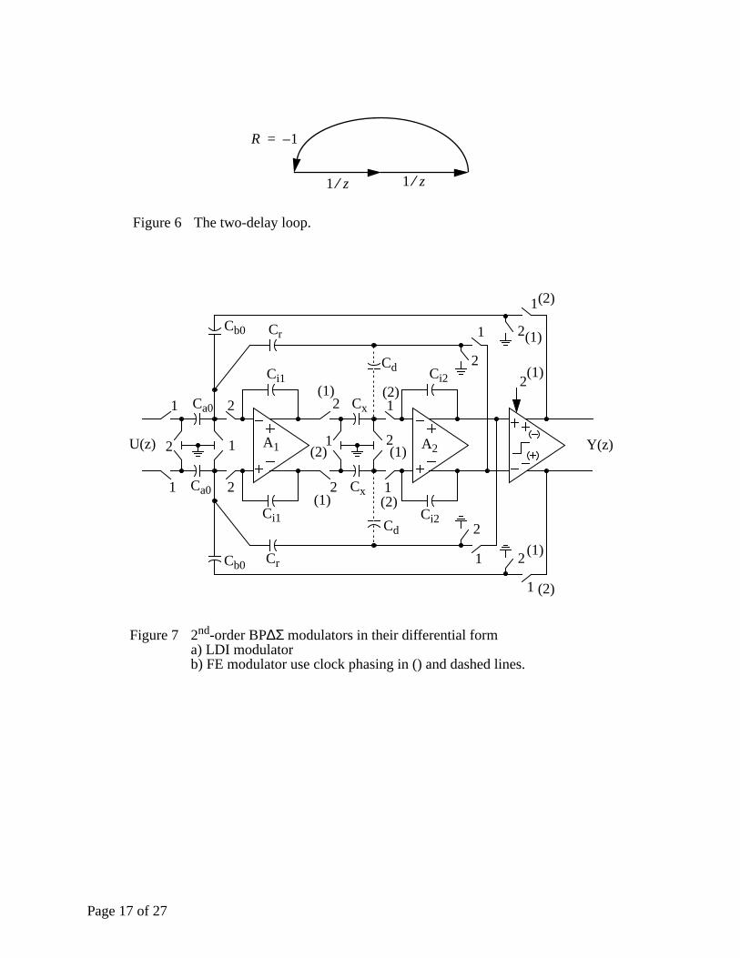
Longo [4] used a switched-C implementation of a pure delay to make the loop shown in Fig. 6,
which has characteristic equation . This is exactly the inverse of the LDI loop in the sense
that the angle (frequency) of the poles is fixed, but the magnitude (notch depth) is sensitive to loop
gains. This structure can only be used for the particular case of bandpass modulators centered at
.
SC FILTER DESIGN
The loops of Fig. 4 to Fig. 6 can be implemented in switched-C technology in a number of ways,
resulting in different demands on the op-amps. We compare them first using an optimistic simple
model of an op-amp as a pure transconductor, modelling the effects of finite op-amp gain and
slew-rate in a second pass.
The LDI loop, in particular, can be implemented either with the timing used in [3], where both op-
amps are connected together during settling or so that they are decoupled [19]. We decoupled the
op-amps for settling, obtaining the modulator design shown in Fig. 7. (ignore clock phasings in
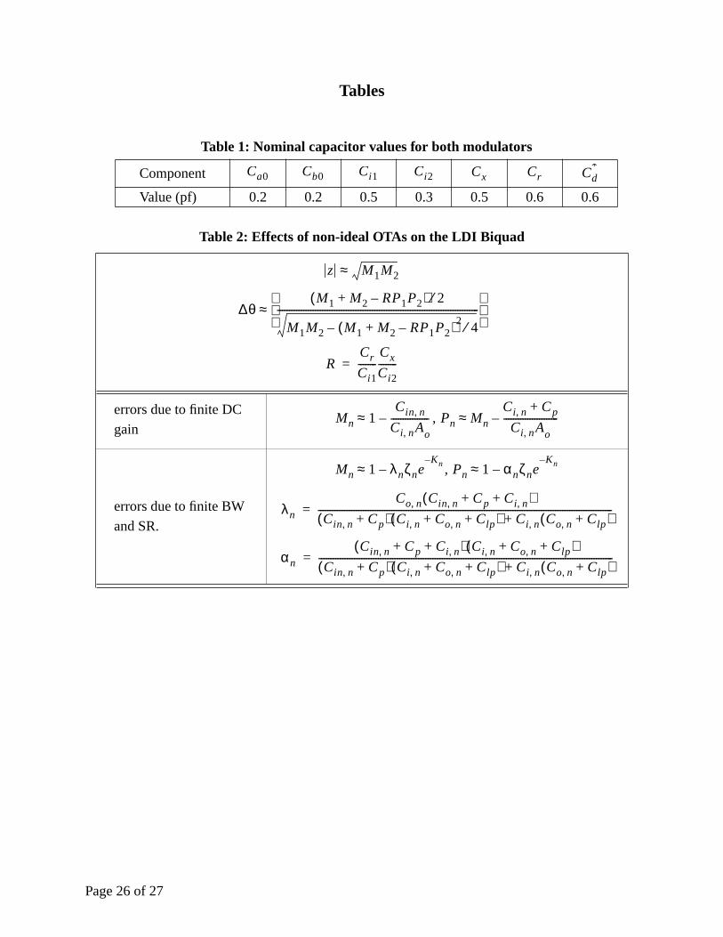
parentheses “()” and connections shown as dashed lines at this point) Component values are as
given in Table 1.
R 2–= f s 4⁄
1 z 1–( )⁄
z z 1–( )⁄
D
z2 2 D+( )– z 1 R– D+( )+ R D 2–= = f s 4⁄
R D
R
z2 α–
f s 4⁄
Page 5 of 27
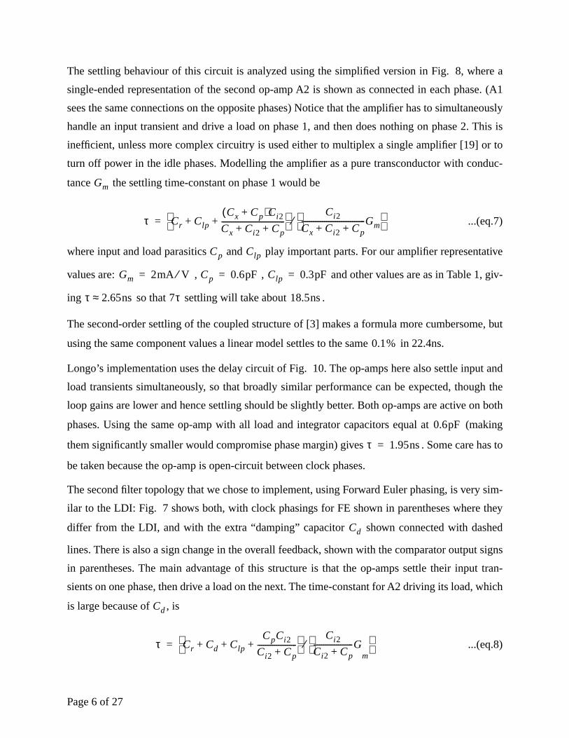
The settling behaviour of this circuit is analyzed using the simplified version in Fig. 8, where a
single-ended representation of the second op-amp A2 is shown as connected in each phase. (A1
sees the same connections on the opposite phases) Notice that the amplifier has to simultaneously
handle an input transient and drive a load on phase 1, and then does nothing on phase 2. This is
inefficient, unless more complex circuitry is used either to multiplex a single amplifier [19] or to
turn off power in the idle phases. Modelling the amplifier as a pure transconductor with conduc-
tance the settling time-constant on phase 1 would be
...(eq.7)
where input and load parasitics and play important parts. For our amplifier representative
values are: , , and other values are as in Table 1, giv-
ing so that settling will take about .
The second-order settling of the coupled structure of [3] makes a formula more cumbersome, but
using the same component values a linear model settles to the same in 22.4ns.
Longo’s implementation uses the delay circuit of Fig. 10. The op-amps here also settle input and
load transients simultaneously, so that broadly similar performance can be expected, though the
loop gains are lower and hence settling should be slightly better. Both op-amps are active on both
phases. Using the same op-amp with all load and integrator capacitors equal at (making
them significantly smaller would compromise phase margin) gives . Some care has to
be taken because the op-amp is open-circuit between clock phases.
The second filter topology that we chose to implement, using Forward Euler phasing, is very sim-
ilar to the LDI: Fig. 7 shows both, with clock phasings for FE shown in parentheses where they
differ from the LDI, and with the extra “damping” capacitor shown connected with dashed
lines. There is also a sign change in the overall feedback, shown with the comparator output signs
in parentheses. The main advantage of this structure is that the op-amps settle their input tran-
sients on one phase, then drive a load on the next. The time-constant for A2 driving its load, which
is large because of , is
...(eq.8)
Gm
τ Cr Clp
Cx Cp+( )Ci2
Cx Ci2 Cp+ +----------------------------------+ +
Ci2
Cx Ci2 Cp+ +----------------------------------Gm
⁄=
Cp Clp
Gm 2mA V⁄= Cp 0.6pF= Clp 0.3pF=
τ 2.65ns≈ 7τ 18.5ns
0.1%
0.6pF
τ 1.95ns=
Cd
Cd
τ Cr Cd Clp
CpCi2
Ci2 Cp+---------------------+ + +
Ci2
Ci2 Cp+---------------------G
m ⁄=
Page 6 of 27
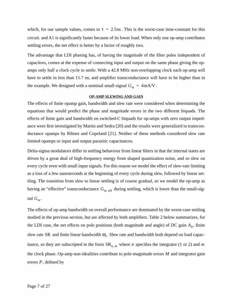
which, for our sample values, comes to . This is the worst-case time-constant for this
circuit. and A1 is significantly faster because of its lower load. When only one op-amp contributes
settling errors, the net effect is better by a factor of roughly two.
The advantage that LDI phasing has, of having the magnitude of the filter poles independent of
capacitors, comes at the expense of connecting input and output on the same phase giving the op-
amps only half a clock cycle to settle. With a 42.8 MHz non-overlapping clock each op-amp will
have to settle in less than 11.7 ns, and amplifier transconductance will have to be higher than in
the example. We designed with a nominal small-signal .
OP-AMP SLEWING AND GAIN
The effects of finite opamp gain, bandwidth and slew rate were considered when determining the
equations that would predict the phase and magnitude errors in the two different biquads. The
effects of finite gain and bandwidth on switched-C biquads for op-amps with zero output imped-
ance were first investigated by Martin and Sedra [20] and the results were generalized to transcon-
ductance opamps by Ribner and Copeland [21]. Neither of these methods considered slew rate
limited opamps or input and output parasitic capacitances.
Delta-sigma modulators differ in settling behaviour from linear filters in that the internal states are
driven by a great deal of high-frequency energy from shaped quantization noise, and so slew on
every cycle even with small input signals. For this reason we model the effect of slew-rate limiting
as a loss of a few nanoseconds at the beginning of every cycle during slew, followed by linear set-
tling. The transition from slew to linear settling is of course gradual, so we model the op-amp as
having an “effective” transconductance during settling, which is lower than the small-sig-
nal .
The effects of op-amp bandwidth on overall performance are dominated by the worst-case settling
studied in the previous section, but are affected by both amplifiers. Table 2 below summarizes, for
the LDI case, the net effects on pole positions (both magnitude and angle) of DC gain , finite
slew rate and finite linear bandwidth . Slew rate and bandwidth both depend on load capac-
itance, so they are subscripted in the form where specifies the integrator (1 or 2) and
the clock phase. Op-amp non-idealities contribute to pole-magnitude errors and integrator gain
errors , defined by
τ 2.5ns=
Gm 4mA/V=
Gm eff,
Gm
A0
SR ωt
SRn m, n m
M
P
Page 7 of 27
...(eq.9)
In the ideal integrator . Errors in the individual integrators then produce magnitude
and angle errors in the overall poles according to the formula in the first row of the table. Notice
that the gain does not affect , as we know for LDI. The second row of the table shows how
finite gain affects and , while the third row shows the effects of slew rate and bandwidth
(via ).
Auxiliary terms used in modelling bandwidth effects are
...(eq.10)
...(eq.11)
...(eq.12)
...(eq.13)
is a scaling factor for the slew rate errors; is the expected step size for slewing, which we
take to be the reference voltage for the A/D; is the number of time-constants of linear settling
available after penalizing for slew and the “non-overlap” time ; is the linear settling time con-
stant; represents all the capacitors connected to the input of the opamp, not including the
input parasitic; is the integrating capacitor; is the parasitic capacitance at the input of the
opamp; is the parasitic capacitance at the output of the op-amp and is the total capacitive
load on the op-amp output, including parasitics and the feedback network. In the tables refers
to all the capacitors which are connected from the output of the opamp to ground, not including
the output parasitic.
The errors for the FE biquad are given in Table 3 in a similar fashion.
OP-AMP AND COMPARATOR CIRCUITS
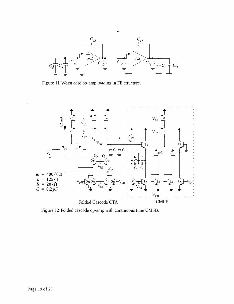
A fully differential folded cascode opamp with continuous time common mode feedback was
designed in the BiCMOS process (Fig. 12). An infinite input impedance was required for
the switched-C filters to avoid charge leakage, so we used MOS inputs. PMOS devices were used
so that the much faster NPN bipolar devices could be used as the cascoding devices that set the
Vo z( )
Vi z( )------------
Cin Ci⁄( )P
z M–--------------------------=
M P 1= =
R z
Mn Pn
Gm eff,
ωt Gm eff, CL⁄=
τ Cin Cp Ci+ +( ) Ciωt( )⁄=
ζ τ SR( ) Vstep⁄=
K 1 τ⁄( ) 12 f s--------
Vstep
SR-----------– τ tol–+
=
ζ Vstep
K
tol τ
Cin
Ci Cp
Clp CL
Co
0.8µm
Page 8 of 27
second pole to roughly its . The simulated parameters for the folded cascode opamp are given in
Table 4.
An NMOS-NPN (non-folded) cascode has the potential for even faster operation, or for better
power efficiency, but is more sensitive to bias errors. We chose to leave it for a later revision, and
are fabricating a prototype.
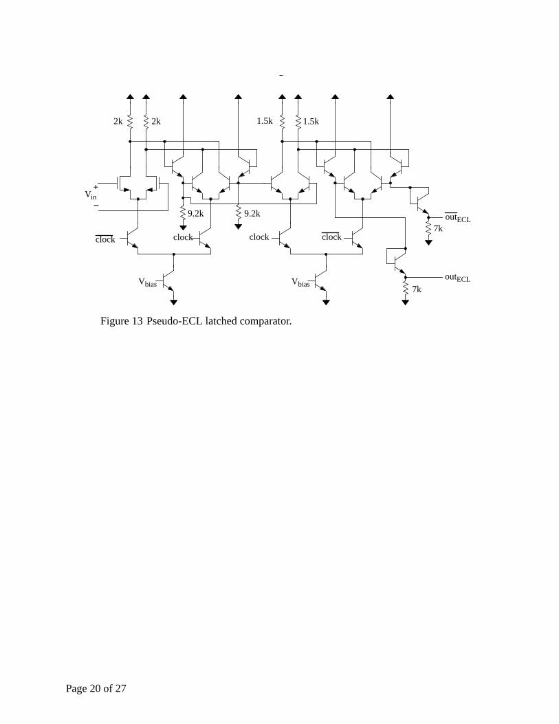
The comparator (Fig. 13) was a version of an existing part [22] modified by replacing bipolar
inputs with NMOS devices so as not to load amplifier A2 at DC. (which would reduce its gain and
settling accuracy) It has approximately eight-bit accuracy at 200 MHz, which is sufficient for our
modulators, since circuits are known to be tolerant of comparator offsets and hysteresis. It
consumes 10mW.
The overall circuit consumes 60mW (experimentally). In a time-division multiple-access receiver
application where it need only be active of the time the average power would be under
10mW.
EXPERIMENTAL RESULTS
Fig. 14 is a photomicrograph showing both the FE (labelled “SigDel2ph” on the layout in refer-
ence to the two-phase delay around the loop) and LDI (SigDelLDI) BP∆Σ modulators. Test struc-
tures were also fabricated for an individual op-amp and a switched-C settling test circuit. The op-
amp tested alone showed a DC gain of , and the settling tester responded to a differ-
ential step with a 10% to 90% rise-time of ; that included approximately of slewing.
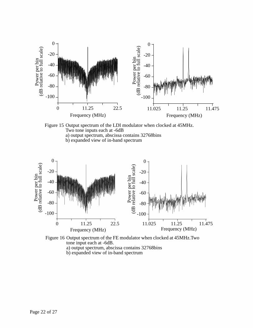
A typical output spectrum, one for the LDI BP∆Σ modulator when clocked at 45 MHz, is shown
in Fig. 15a. It broadly matches the simulated spectrum in shape (with a fatter noise band attribut-
able to the larger variance expected from using a larger number of bins), but has significant tone
power well out of band at about and of the clock frequency. The FE modulator produces
a very similar spectrum, as shown in Fig. 16a.
Fig. 15b and Fig. 16b are expanded in-band plots measuring in-band SNR and intermodulation
distortion for the two modulators. Two input tones, each 6dB below the saturation level, were
applied in-band. (this was also the case for Fig. 15a and Fig. 16a, but the two tones are too close
to distinguish on that scale) Clock and input frequency generators were asynchronous, so the
input tones are not confined to a single FFT bin, and there is also sideband power from both fre-
quency sources. Note that the spectra in these experiments are obtained digitally, rather than (as is
f t
∆Σ
1 8⁄
55dB 1.6V
3.3ns 1.2ns
1 8⁄ 3 8⁄
Page 9 of 27
commonly done) simply by running the digital stream into an analog spectrum analyzer. The latter
technique can be misleading because it hides the effects of clock jitter.
In-band noise is evaluated by averaging noise power over the band of interest. The noise compo-
nents are averaged over FFT bins of bandwidth . Intermodulation
products are below the noise for the LDI case but peaks are clearly visible in the FE case (Fig.
16b) at about . The third-order intercept point is thus relative to the saturation
level for the FE case, and somewhat higher for the LDI.
The in-band spectra slope to the left, which shows that the notch is slightly low, and we attribute
this partly to capacitor ratio errors and partly to finite DC gain and incomplete settling. The prob-
lem is much more evident for the LDI case, which we would expect from our settling analysis.
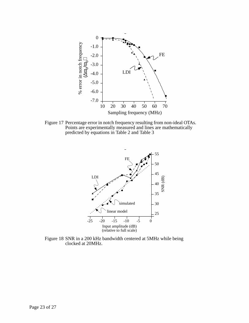
In order to separate the effects of DC errors and incomplete settling, bit streams were obtained for
both modulators at several different clock frequencies. A Hanning-windowed 65536 point. FFT
was performed on the bit streams and the notch frequency was determined to give the points plot-
ted in Fig. 17. Assuming that the gain from the test op-amp applied to the modulators, a
+0.3% error in the capacitor ratio Cd/Ci2 and +0.2% error in the capacitor ratio Cr/Ci1 were esti-
mated to be the capacitor ratio mismatches, resulting in a small frequency error even at low clock
rates. These mismatches are quite plausible given the small unit capacitor value we are using. The
plot shows that settling is essentially complete below about 30MHz and that the FE structure is
still good to 1% at the 42.8MHz clock needed for a 10.7MHz IF.
Signal levels were varied at a constant clock frequency of 20MHz, where settling is complete,
producing the plot of SNR against signal level shown as Fig. 18. There is a large deviation from
the straight-line behaviour predicted by the linear model and by simulations: this is similar to the
characteristic already known for first-order lowpass ∆Σ modulators in the presence of a small off-
set, and which should be expected for second-order bandpass. It suggests that tones tend to be out-
of-band at low input levels, making for anomalously good SNR.
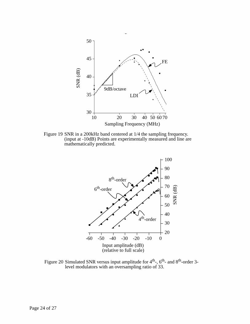
Fig. 19 summarizes the effect of changing clock rate on SNR in a given bandwidth. At low clock
rates there is insufficient oversampling to get good SNR, and when the clock rate exceeds about
the notch frequency drifts off-centre and reduces SNR again. The measurements were
made with the signal 10dB below saturation (where Fig. 18 shows that we only have about 45dB
of SNR) The best SNR is obtained for the FE structure near the nominal 42.8MHz, and is about
47dB relative to the -10dB input signal, giving a peak SNR of 57dB relative to the modulator’s
22.5MHz 32768⁄ 686Hz≈
60dB– +28dB
55dB
40MHz
Page 10 of 27
saturation level. The curve shows experimental SNR together with the mathematical model of
Table 2 and Table 3. The mathematical fit is not nearly as good as for Fig. 17 because SNR mea-
surements are affected by non-ideal tone behaviour whereas notch frequencies are set accurately
by the behaviour of the linear filter.
OBTAINING A 1MHZ BANDWIDTH
As mentioned in the Introduction, some base-station applications need bandwidths of about
1.2MHz. Pushing the technology of this paper to 80MHz clocking (as simulation suggests may be
possible) would give an oversampling ratio of , which is quite low. The
high linearity requirements of digital radio may be a problem for the multi-bit or MASH
approaches that tend to be used at low oversampling rates, but digital correction to the 20-bit level
has recently been demonstrated for a three-state feedback A/D [23]. On the assumption that this is
possible for bandpass conversion, and designing a noise transfer function according to the method
of [3] with split notches and a conservative 5dB of out-of-band gain, Fig. 20 shows the SNR per-
formance that can be expected for modulators of order four, six and eight. Although an eighth-
order modulator sounds very aggressive, recall that it has the dynamics of a fourth-order lowpass
converter, of which examples are in commercial use.
CONCLUSIONS
Switched-capacitor bandpass technology appears to be practical for A/D conversion of radio
IF signals at , although a production version of the chip would need an improved op-
amp (particularly to improve slew rate, and also to reduce power consumption) to get the perfor-
mance margin needed to cover process and temperature variation. We have initial simulations
showing that an op-amp almost twice as fast should be possible in the same process, using a sim-
ple rather than folded cascode, and a test version is in fabrication.
A second-order modulator gives a 57dB SNR in a 200kHz bandwidth when clocked at the nomi-
nal , but shows pronounced non-ideal noise behaviour. Using a fourth-order structure
(shown to work at lower clock rates in [3] and [4]) with the high-speed technology demonstrated
here should give improved bandwidth and SNR, which in turn should give more margin and flexi-
bility to the system designer. A bandwidth of about 1MHz seems attainable with present technol-
ogy, and at high order would benefit from the use of a three-level quantizer.
Forward-Euler switch phasing gives a significant speed advantage over LDI, and its sensitivity to
ratio errors does not appear to seriously degrade SNR. High-order quantizers with high relative
40MHz 1.2MHz⁄ 33.3=
∆Σ
10.7MHz
42.8MHz
Page 11 of 27
bandwidths tend to be less sensitive to magnitude errors in the poles, so the FE structure should
work even better there. A structure like that of [4][24] may have even better speed, but was not
compared on the same process as the LDI and FE circuits. At high clock rates it is more important
to design switched-C circuits for rapid amplifier settling than for low passive sensitivities.
ACKNOWLEDGMENTS
Fabrication of the chip was provided by Northern Telecom, and design and partial financial sup-
port by Bell Northern Research. The remaining financial support came from the Micronet pro-
gram and from an OCRI/NSERC Industrial Research Chair. Test jigs were designed by Luc
Lussier, and much of the testing and debugging done by Theodore Varelas.
REFERENCES
[1] R. Hadaway, et al, “A Sub-micron BiCMOS Technology for Telecommunications,” J. ofMicroelectronic Engineering, vol. 15, pp. 513-516, 1991.
[2] Jack M. Holtzman and David J. Goodman, “Wireless Communications: Future Directions,”Kluwer 1993.
[3] S. A. Jantzi, W. M. Snelgrove, and P. F. Ferguson Jr., “A fourth order bandpass sigma-deltamodulator,” IEEE J. Solid-State Circuits, vol. 28, pp. 282-291, pp. 282-291, March 1993.
[4] Lorenzo Longo and Bor-Rong Hong, “A 15b 30kHz Bandpass Sigma-Delta Modulator,”ISSCC-93 Digest pp. 226-227.
[5] O. Shoaei and M. Snelgrove, “Optimal (Bandpass) Continuous-Time Sigma - Delta Modula-tor,” Proc. ISCAS 94, London, Eng., v. 5 pp. 489-492 May 30-June 2 1994.
[6] G. Troster, et al., “An interpolative bandpass converter on a 1.2 sum BiCMOS analog/digitalarray,” IEEE J. Solid-State Circuits, vol. 28, no. 4, pp. 471-477, April 1993.
[7] B.P. Brandt and B.W. Wooley, “A 50MHz multibit sigma-delta modulator for 12-bit 2MHz A/D conversion,” IEEE J. Solid State Circuits, v. 26 #12 pp. 1746-1756, Dec. 1991.
[8] B.S. Song, “A 10.7MHz switched-capacitor bandpass filter,” IEEE J. Solid State Circuits, v.24 #4 pp. 320-334, April 1989.
[9] P.H. Gailus, W.J. Turney, F.R. Yester Jr., “Method and Arrangement for a Sigma Delta Con-verter for Bandpass Signals”, U.S. Patent no. 4,857,928, filed Jan. 28 1988, issued Aug. 151989.
[10] A.M. Thurston, T.H. Pearce and H.J. Hawksford, “Bandpass Implementation of the SigmaDelta A/D Conversion Technique,” IEE Int’l Conf. on Analogue to Digital and Digital to Ana-logue Conversion, Swansea, pp. 81-86 Sept. 1991.
[11] B.P. Brandt and B.A. Wooley, “A Low-Power, Area-Efficient Digital Filter for Decimationand Interpolation,” IEEE J. Solid State Circuits, v. 29 #6 pp. 679-687 June 1994.
[12] Inose and Yasuda, “A unity bit coding method by negative feedback,” Proceedings of theIEEE, vol. 51, pp. 1524-1535, Nov. 1963.
[13] R. Schreier and M. Snelgrove, “Bandpass Sigma-Delta Modulation”, Electron. Lett., v. 25,#23, pp. 1560-1561, Nov. 1989.
[14] W. Chou and R. M. Gray, “Dithering and its effects on sigma-delta and multi-stage sigma-delta modulation,” IEEE Proc. ISCAS’90, pp. 368-371, May 1990.
[15] S. R. Norsworthy, R. Schreier and G.C. Temes, eds., “Delta-Sigma Data Converters,” IEEEPress, to appear.
[16] O. Feely and L.O. Chua, “The Effect of Integrator Leak in Sigma-Delta Modulation,” IEEE
Page 12 of 27
Trans. Circuits Syst., v. 38, #11, pp. 1293-1305, Nov. 1991[17] S.R. Norsworthy, I.G. Post, H.S. Fetterman, “A 14-bit 80-kHz sigma-delta A/D converter:
modeling, design, and performance evaluations,” IEEE J. Solid-State Circuits, vol. SC-24, pp.256-266, April 1989.
[18] R. Schreier, “Noise-shaped coding,” Ph.D. Thesis, University of Toronto, Toronto, 1991.[19] F. Montecchi, “Time-shared Switched-capacitor filters insensitive to parasitic effects,” IEEE
Trans. Circuits Sys, v. CAS-31, pp. 349-353, April 1984.[20] K. Martin and A. S. Sedra, “Effects of the op amp finite gain and bandwidth on the perfor-
mance of switched-capacitor filters,” IEEE Trans. on Circuits and Systems, vol. cas-28, no. 8,pp. 822-829, August 1981.
[21] D. Ribner and M. Copeland, “Biquad alternatives for high frequency switch-capacitor fil-ters,” IEEE J. Solid-State Circuits, vol. 20, no. 6, pp. 1085-1095, December 1985.
[22] J. R. Long, “High frequency integrated circuit design in BiCMOS for monolithic timingrecovery,” M.Eng. Thesis, Carleton University, Ottawa, Canada, 1992.
[23] Charles D. Thompson and Salvador R. Bernardas, “A Digitally-Corrected 20b Delta-SigmaModulator,” 1994 ISSCC Digest, San Francisco, pp. 194-195 Feb. 1994.
[24] S.H. Lewis, H.S. Fetterman, G.F. Gross, Jr., R. Ramachandran and T.R. Viswanathan, “A 10-b 20Msample/s Analog-to-Digital Converter,” IEEE Journal of Solid State Circuits, vol. 27, #3,pp. 351-358, March 1992
Page 13 of 27
Figure Captions
Figure 1: Block diagram of delta-sigma modulator.
Figure 2: Output spectrum of ideal second order modulator. The abscissa contains 2048 bins.
Figure 3: Linear model prediction of SNR for a 2nd-order modulator which has errors in the mag-nitude and angle of its filter pole. (input at -6dB)
Figure 4: The LDI loop, where pole magnitude is capacitor-insensitive
Figure 5: The Forward-Euler loop.
Figure 6: The two-delay loop.
Figure 7: 2nd-order BP∆Σ modulators in their differential form a) LDI modulator b) FE modulatoruse clock phasing in () and dashed lines.
Figure 8: Op-amp loading in our LDI structure which has op-amps settling in parallel rather thanseries
Figure 9: Op-amp loading in Jantzi structure.
Figure 10: Unit delay circuit used in Longo’s structure.
Figure 11: Worst case op-amp loading in FE structure.
Figure 12: Folded cascode op-amp with continuous time CMFB.
Figure 13: Pseudo-ECL latched comparator.
Figure 14: Photomicrograph of test chip a) Folded cascode opamp b) Switched-C unity gain con-figuration c) Forward Euler BPDS modulator d) LDI BPDS modulator
Figure 15: Output spectrum of the LDI modulator when clocked at 45MHz. Two tone inputs eachat -6dB a) output spectrum, abscissa contains 32768bins b) expanded view of in-bandspectrum
Figure 16: Output spectrum of the FE modulator when clocked at 45MHz.Two tone input each at-6dB. a) output spectrum, abscissa contains 32768bins b) expanded view of in-bandspectrum
Figure 17: Percentage error in notch frequency resulting from non-ideal OTAs. Points are experi-mentally measured and lines are mathematically predicted by equations in Table 2 andTable 3
Figure 18: SNR in a 200 kHz bandwidth centered at 5MHz while being clocked at 20MHz.
Figure 19: SNR in a 200kHz band centered at 1/4 the sampling frequency. (input at -10dB) Pointsare experimentally measured and line are mathematically predicted.
Figure 20: Simulated SNR versus input amplitude for 4th-, 6th- and 8th-order 3-level modulatorswith an oversampling ratio of 33.
Page 14 of 27
Figures
filter
Bit streamout
Analog input
N
Y
YXU
X
A(z)
Figure 1 Block diagram of delta-sigma modulator.
0
-20
-40
-60
-80
0 π/4 π/2 3π/4 πNormalized frequency (rad/s)
Pow
er p
er b
in(d
B r
elat
ive
to f
ull s
cale
)
Figure 2 Output spectrum of ideal second order modulator. The abscissa con-tains 2048 bins.
Page 15 of 27
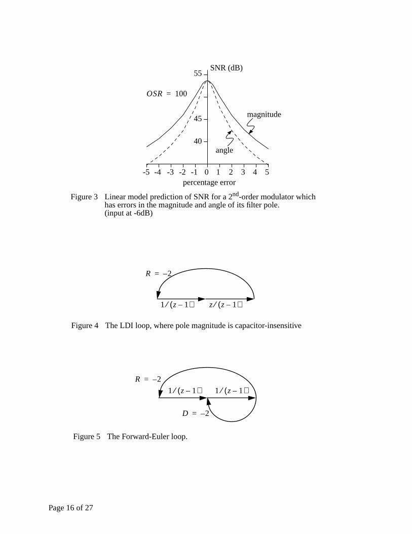
-5 -4 -3 -2 -1 0 1 2 3 4 5
SNR (dB)
percentage error
magnitude
angle
55
45
40
OSR 100=
Figure 3 Linear model prediction of SNR for a 2nd-order modulator which has errors in the magnitude and angle of its filter pole.(input at -6dB)
1 z 1–( )⁄ z z 1–( )⁄
R 2–=
Figure 4 The LDI loop, where pole magnitude is capacitor-insensitive
1 z 1–( )⁄ 1 z 1–( )⁄R 2–=
Figure 5 The Forward-Euler loop.
D 2–=
Page 16 of 27
1 z⁄ 1 z⁄
R 1–=
Figure 6 The two-delay loop.
(2)21
(1)2
(1)2 12
2
1
Ci1
Ci1
A1 A2
Cr
Cd
Cb0
1
1
2
Ca0
Ca0
CrCb0
Cd
Ci2
Ci2
Cx
Cx
Y(z)U(z)
(2)
1(2)
(1)
2(1)
1 (2)
1
2
2(1)
2(1)
1(2)
1
2
Figure 7 2nd-order BP∆Σ modulators in their differential forma) LDI modulatorb) FE modulator use clock phasing in () and dashed lines.
Page 17 of 27
Figure 8 Op-amp loading in our LDI structure which has op-amps set-tling in parallel rather than series
Ci2
CxCr
Cp Clp
A2
Ci2
Cp Clp
A2
Phase 1 Phase 2
Cx
Ci2
Cp Clp Cp Clp
Ci1
Figure 9 Op-amp loading in Jantzi structure.
A1 A2
Cr
C2
C1 C3
Cp Clp
C4
ViNext stage
A
1
2
2 2
2
2
1 1
1
1
2
2
1
1
Figure 10 Unit delay circuit used in Longo’s structure.
Page 18 of 27
Ci2
Cx Cr
Cp Clp
A2
Ci2
Cp Clp
A2
Cd
Figure 11 Worst case op-amp loading in FE structure.
Cd
Vb4 Vb4
Vin
Vout
Vb3
Vb2
Vb1
VcmVcm
CL
Vcm
Vb4
R R
C C
Vb1
Vb2
CL
2x 2x2x 2x
2x2x
1x1x 1x 1x 1x
1x
1x 1x
1.2
mA
CMFB
2aa a
aa2a
a
a
Folded Cascode OTA
Q1Q2m/2 m/2
P2
Figure 12 Folded cascode op-amp with continuous time CMFB.
a 125 1⁄=R 20kΩ=C 0.2 pF=
m m
m 400 0.8⁄=
Page 19 of 27
VbiasVbias
clockclock
2k
clock
9.2k 9.2k
1.5k1.5k
7k
7k
Vin+
_
outECL
outECL
clock
Figure 13 Pseudo-ECL latched comparator.
2k
Page 20 of 27
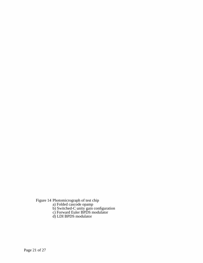
Figure 14 Photomicrograph of test chipa) Folded cascode opampb) Switched-C unity gain configurationc) Forward Euler BPDS modulatord) LDI BPDS modulator
Page 21 of 27
0
-20
-40
-60
-80
-100
0
-20
-40
-60
-80
-100
0 11.25 22.5 11.2511.025 11.475Frequency (MHz)
Pow
er p
er b
in
(dB
rel
ativ
e to
ful
l sca
le)
Frequency (MHz)
Pow
er p
er b
in(d
B r
elat
ive
to f
ull s
cale
)
Figure 15 Output spectrum of the LDI modulator when clocked at 45MHz. Two tone inputs each at -6dBa) output spectrum, abscissa contains 32768binsb) expanded view of in-band spectrum
0
-20
-40
-60
-80
-100
0 11.25 22.5
0
-20
-40
-60
-80
-100
11.2511.025 11.475Frequency (MHz) Frequency (MHz)
Pow
er p
er b
in(d
B r
elat
ive
to f
ull s
cale
)
Pow
er p
er b
in(d
B r
elat
ive
to f
ull s
cale
)
Figure 16 Output spectrum of the FE modulator when clocked at 45MHz.Two tone input each at -6dB.a) output spectrum, abscissa contains 32768binsb) expanded view of in-band spectrum
Page 22 of 27
Sampling frequency (MHz)
% e
rror
in n
otch
fre
quen
cy(∆
ωο/
ωο)
0
-1.0
-2.0
-3.0
-4.0
-5.0
-6.0
-7.010 20 30 40 50 60 70
LDI
FE
Figure 17 Percentage error in notch frequency resulting from non-ideal OTAs. Points are experimentally measured and lines are mathematically predicted by equations in Table 2 and Table 3
55
50
45
40
35
30
25
0-5-10-15-20-25
SNR
(dB
)
Input amplitude (dB)(relative to full scale)
linear model
simulated
FE
LDI
Figure 18 SNR in a 200 kHz bandwidth centered at 5MHz while being clocked at 20MHz.
Page 23 of 27
FE
LDI
10 20 30 40 50 60 70
50
45
40
35
30
Sampling Frequency (MHz)
SNR
(dB
)
9dB/octave
Figure 19 SNR in a 200kHz band centered at 1/4 the sampling frequency. (input at -10dB) Points are experimentally measured and line are mathematically predicted.
100
90
80
70
60
50
40
30
200-10-20-30-40-50-60
Input amplitude (dB)(relative to full scale)
SNR
(dB
)
4th-order
6th-order
8th-order
Figure 20 Simulated SNR versus input amplitude for 4th-, 6th- and 8th-order 3-level modulators with an oversampling ratio of 33.
Page 24 of 27

Tables
Table 1: Nominal capacitor values for both modulators
Table 2: Effects of non-ideal OTAs on the LDI Biquad
Table 3: Effects of non-ideal op-amps on the FE biquad
Table 4: Simulated Performance of the Folded Cascode Amplifier
Page 25 of 27
Tables
Table 1: Nominal capacitor values for both modulators
Component
Value (pf) 0.2 0.2 0.5 0.3 0.5 0.6 0.6
Table 2: Effects of non-ideal OTAs on the LDI Biquad
errors due to finite DC
gain,
errors due to finite BW
and SR.
,
Ca0 Cb0 Ci1 Ci2 Cx Cr Cd*
z M1M2≈
∆θM1 M2 RP1P2–+( ) 2⁄
M1M2 M1 M2 RP1P2–+( )24⁄–
-------------------------------------------------------------------------------------
≈
RCr
Ci1--------
Cx
Ci2--------=
Mn 1Cin n,
Ci n, Ao
----------------–≈ Pn Mn
Ci n, Cp+
Ci n, Ao
-----------------------–≈
Mn 1 λnζneKn–
–≈ Pn 1 αnζneKn–
–≈
λn
Co n, Cin n, Cp Ci n,+ +( )Cin n, Cp+( ) Ci n, Co n, Clp+ +( ) Ci n, Co n, Clp+( )+
----------------------------------------------------------------------------------------------------------------------------=
αn
Cin n, Cp Ci n,+ +( ) Ci n, Co n, Clp++( )Cin n, Cp+( ) Ci n, Co n, Clp++( ) Ci n, Co n, Clp+( )+
----------------------------------------------------------------------------------------------------------------------------=
Page 26 of 27
Table 3: Effects of non-ideal op-amps on the FE biquad
,
errors due to finite DC
gain,
errors due to finite BW
and SR.
Table 4: Simulated Performance of the Folded Cascode Amplifier
Parameter Value
DC gain 57dB
Unity-gain frequency 500MHz
Phase-margin 75o
Settling time to 0.1% 9.0ns
Slew-rate 1000V/µs
Differential output range 5.2V
Power consumption 26mW
measurements for a 1pF load capacitor
z M1M2 RP1P2 DP2M1–+≈
∆θM1 M2 DP2–+( ) 2⁄
z2
M1 M2 RP2–+( )24⁄–
----------------------------------------------------------------------
≈
RCr
Ci1--------
Cx
Ci2--------= D
Cd
Ci2--------=
Mn 1Cin n,
Ci n, Ao
----------------–≈ Pn Mn
Ci n, Cp+
Ci n, Ao
-----------------------–≈
Mn 1 λnζn 2, eKn 2,–
–≈
Pn 1 αnζn 1, eKn 1,–
–( ) 1 λnζn 2, eKn 2,–
–( )≈
λn
Co n,Co n, Clp Ci n, Cp Ci n, Cp+( )⁄+ +---------------------------------------------------------------------------------=
αn
Cin n, Cp Ci n,+ +
Cin n, Cp Ci n, Clp Ci n, Clp+( )⁄+ +-----------------------------------------------------------------------------------=
Page 27 of 27