supra-hierarchical nano-structured organic thin …supra-hierarchical nano-structured organic thin...
TRANSCRIPT
Supra-hierarchical nano-structured organic thin film solar cell
Institute of Advanced EnergyKyoto University
Susumu Yoshikawa
3rd Japan-German Bilateral Workshop on Molecular Electronics
21-23, Jan., 2009, 烏丸 Kyoto Hotel, Japan
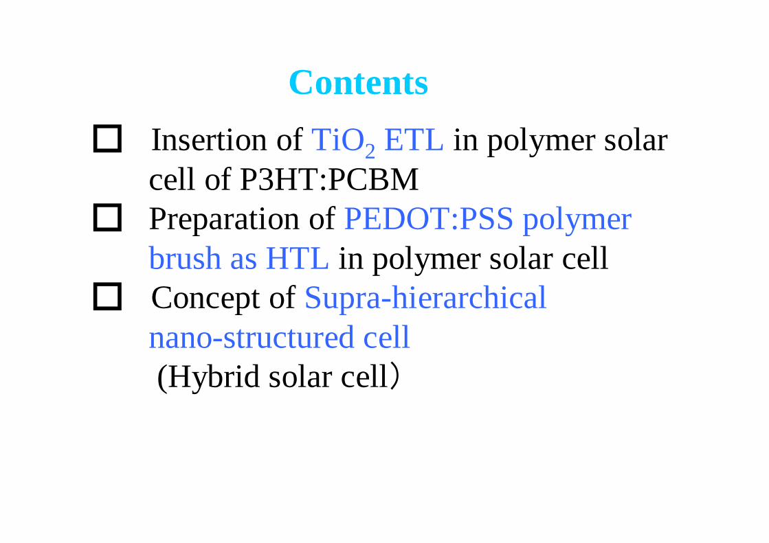
Contents□ Insertion of TiO2 ETL in polymer solar
cell of P3HT:PCBM □ Preparation of PEDOT:PSS polymer
brush as HTL in polymer solar cell□ Concept of Supra-hierarchical
nano-structured cell(Hybrid solar cell)
ITO
Glass
Al
V
Heterojunction(Tang Cell)
ITO
Glass
Al
n-type semiconductor
p-type semiconductor
V
Bulk heterojunction(Sariciftci Cell)with C60
Metal
Glass
Al
V
Schottky junction(Calvin Cell)
organic semi-conductor
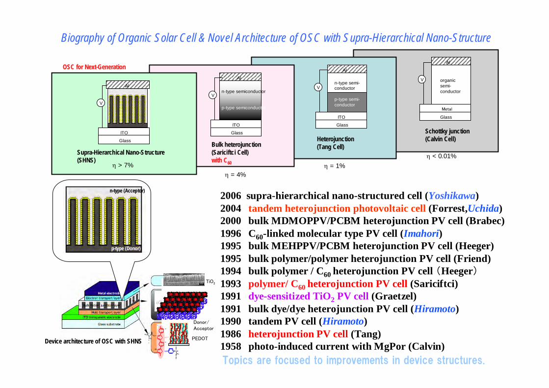
Biography of Organic Solar Cell & Novel Architecture of OSC with Supra-Hierarchical Nano-Structure
Supra-Hierarchical Nano-Structure (SHNS)
Glass
V
Al
CCH2
H 3C CO
OS
S
S
S
CHCH 2
O3S
Device architecture of OSC with SHNS
n-type (Acceptor)
p-type (Donor)
2006 supra-hierarchical nano-structured cell (Yoshikawa)2004 tandem heterojunction photovoltaic cell (Forrest,Uchida)2000 bulk MDMOPPV/PCBM heterojunction PV cell (Brabec)1996 C60-linked molecular type PV cell (Imahori)1995 bulk MEHPPV/PCBM heterojunction PV cell (Heeger)1995 bulk polymer/polymer heterojunction PV cell (Friend)1994 bulk polymer / C60 heterojunction PV cell (Heeger)1993 polymer/ C60 heterojunction PV cell (Sariciftci)1991 dye-sensitized TiO2 PV cell (Graetzel)1991 bulk dye/dye heterojunction PV cell (Hiramoto)1990 tandem PV cell (Hiramoto)1986 heterojunction PV cell (Tang)1958 photo-induced current with MgPor (Calvin)
η < 0.01%η = 1%
η = 4%η > 7%
TiO2
Donor/Acceptor
PEDOT
ITO
OSC for Next-Generation
n-type semi-conductor
p-type semi-conductor
Topics are focused to improvements in device structures.
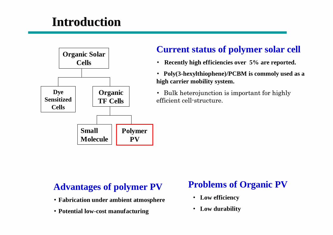
IntroductionIntroduction
Organic Solar Cells
Dye Sensitized
Cells
Organic TF Cells
Small Molecule
Polymer PV
Advantages of polymer PV・ Fabrication under ambient atmosphere
・ Potential low-cost manufacturing
Problems of Organic PV・ Low efficiency
・ Low durability
Current status of polymer solar cell ・ Recently high efficiencies over 5% are reported.
・ Poly(3-hexylthiophene)/PCBM is commoly used as a high carrier mobility system.
・ Bulk heterojunction is important for highly efficient cell-structure.
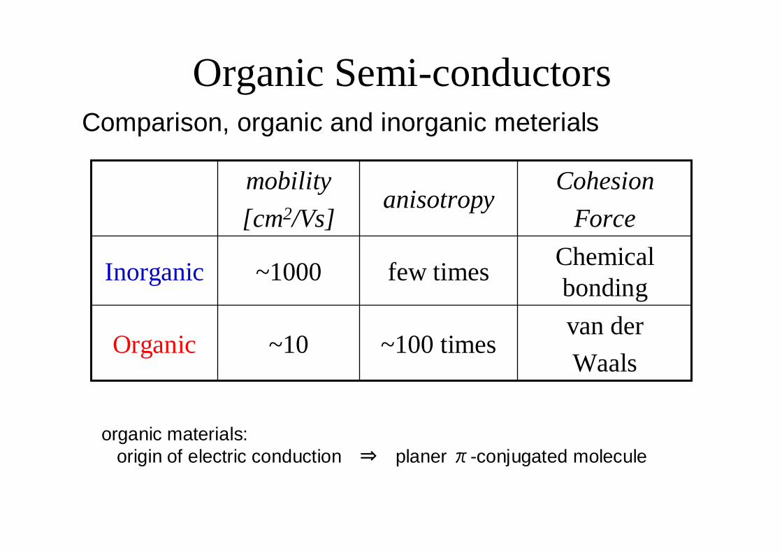
Organic Semi-conductorsComparison, organic and inorganic meterials
~100 times
few times
anisotropy
van derWaals
~10Organic
Chemical bonding~1000Inorganic
CohesionForce
mobility[cm2/Vs]
organic materials:origin of electric conduction ⇒ planer π-conjugated molecule
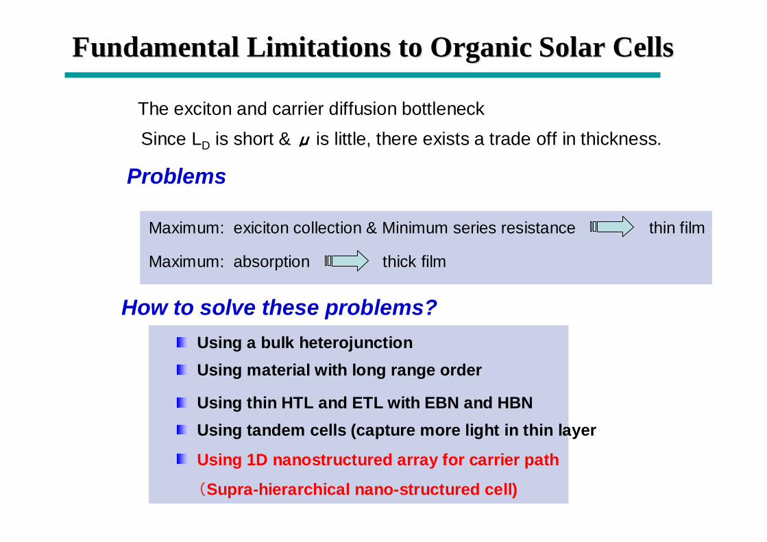
Fundamental Limitations to Organic Solar Cells Fundamental Limitations to Organic Solar Cells
The exciton and carrier diffusion bottleneckSince LD is short & μ is little, there exists a trade off in thickness.
Maximum: exiciton collection & Minimum series resistance thin film
Maximum: absorption thick film
How to solve these problems?Using a bulk heterojunction
Using tandem cells (capture more light in thin layer
Using 1D nanostructured array for carrier path
(Supra-hierarchical nano-structured cell)
Using material with long range order
Using thin HTL and ETL with EBN and HBN
Problems
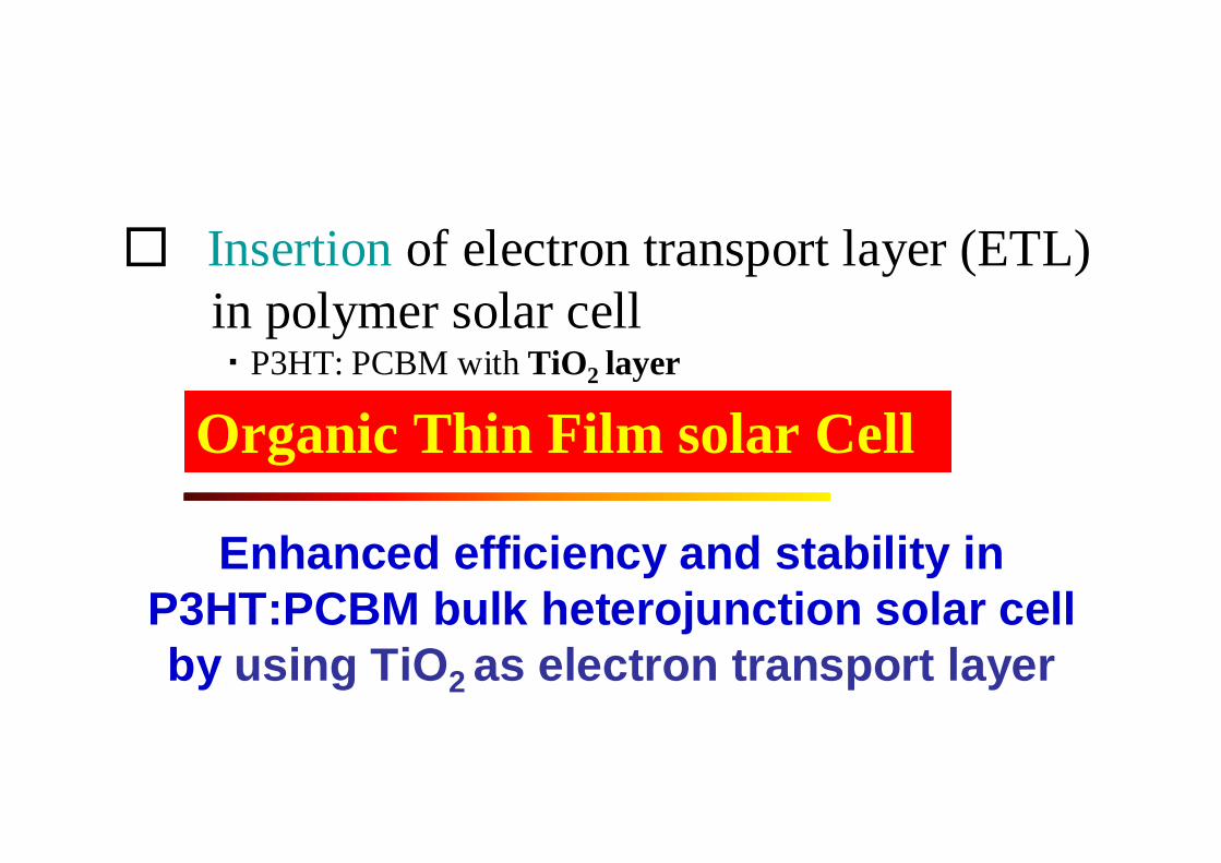
Enhanced efficiency and stability in P3HT:PCBM bulk heterojunction solar cell by using TiO2 as electron transport layer
Organic Thin Film solar Cell
□ Insertion of electron transport layer (ETL) in polymer solar cell・ P3HT: PCBM with TiO2 layer
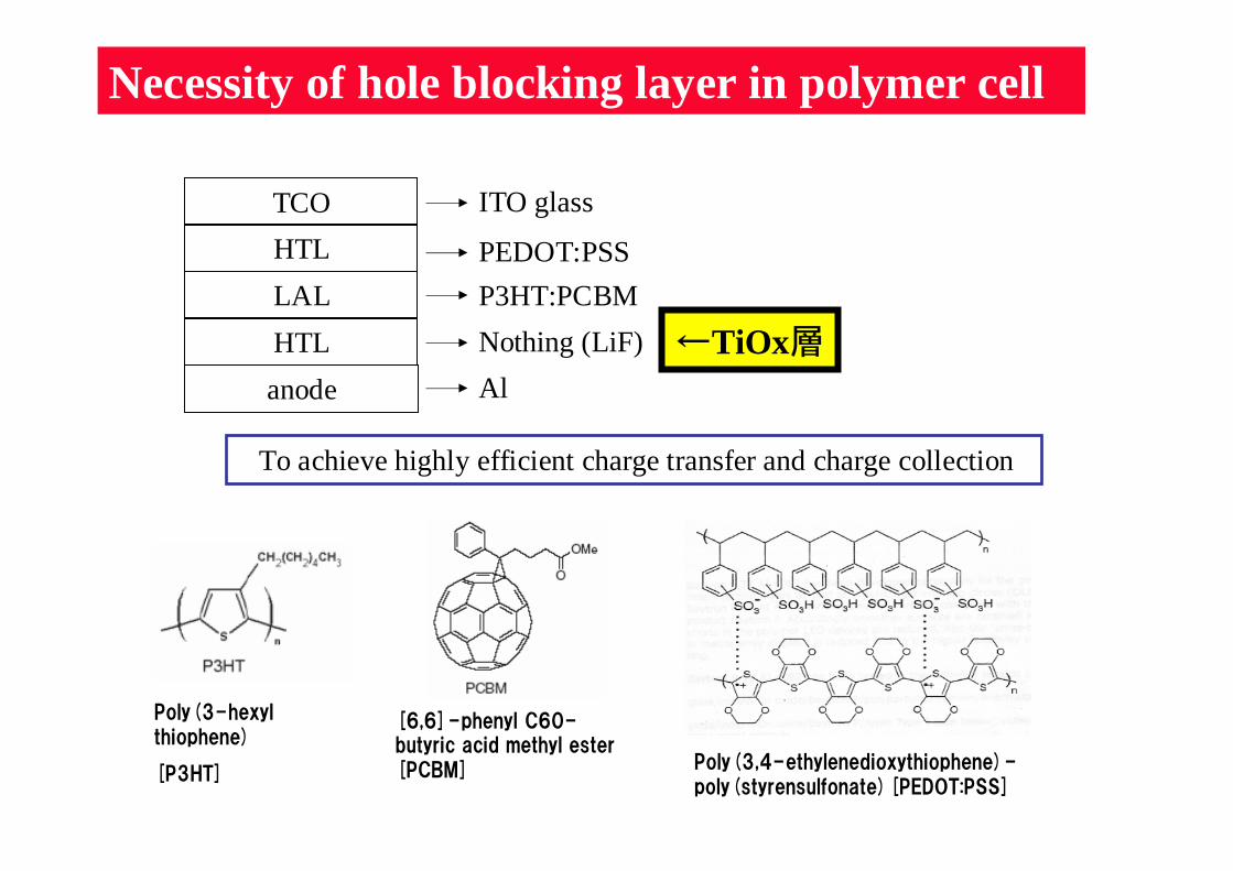
Necessity of hole blocking layer in polymer cell
ITO glassTCOHTLLAL
anodeHTL
PEDOT:PSSP3HT:PCBM
AlNothing (LiF)
To achieve highly efficient charge transfer and charge collection
Poly(3,4-ethylenedioxythiophene)-poly(styrensulfonate)[PEDOT:PSS]
[6,6]-phenyl C60-butyric acid methyl ester [PCBM]
Poly(3-hexyl thiophene)
[P3HT]
←TiOx層
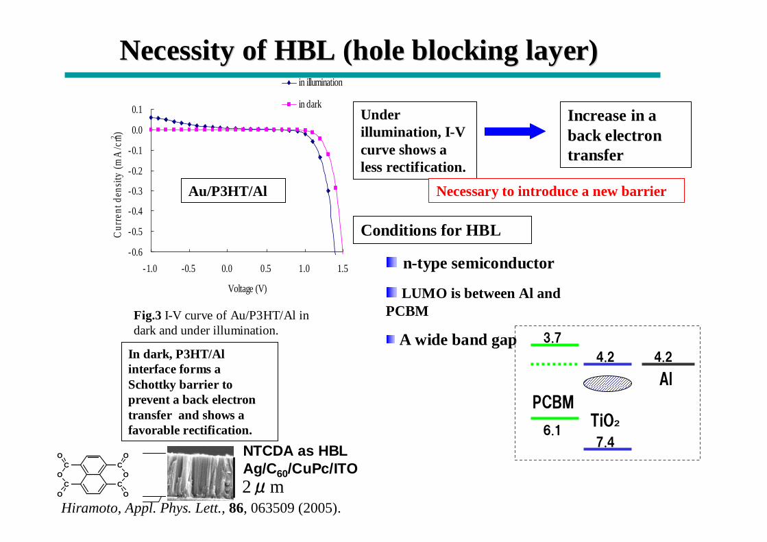
Conditions for HBL
n-type semiconductor
LUMO is between Al and PCBM
A wide band gap4.24.2
7.4
3.7
6.1
Al
TiO₂PCBM
-0.6
-0.5
-0.4
-0.3
-0.2
-0.1
0.0
0.1
-1.0 -0.5 0.0 0.5 1.0 1.5
Voltage (V)
Cur
rent
den
sity
(mA
/cm2 )
in illumination
in darkUnder illumination, I-V curve shows a less rectification.
Increase in a back electron transfer
Au/P3HT/Al
In dark, P3HT/Al interface forms a Schottky barrier to prevent a back electron transfer and shows a favorable rectification.
Necessary to introduce a new barrier
Fig.3 I-V curve of Au/P3HT/Al in dark and under illumination.
Necessity of HBL (hole blocking layer)Necessity of HBL (hole blocking layer)
CO
C
CO
C
O
O
O
O
NTCDA as HBLAg/C60/CuPc/ITO2μm
Hiramoto, Appl. Phys. Lett., 86, 063509 (2005).
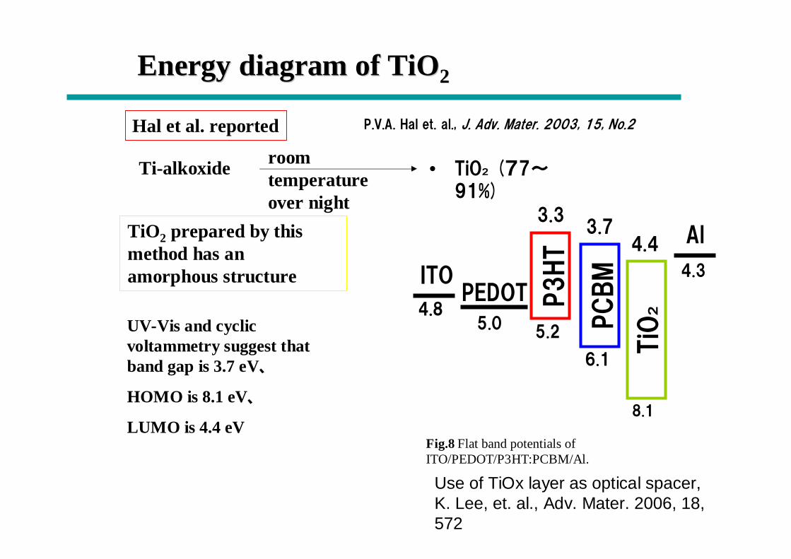
Hal et al. reported
Ti-alkoxide room temperature over night
• TiO₂ (77~91%)
UV-Vis and cyclic voltammetry suggest that band gap is 3.7 eV、
HOMO is 8.1 eV、
LUMO is 4.4 eV
ITO
4.8PEDOT
5.0
P3HT
5.2
3.3
PCBM
6.1
3.7 Al
4.3
TiO
₂
4.4
8.1
TiO2 prepared by this method has an amorphous structure
Fig.8 Flat band potentials of ITO/PEDOT/P3HT:PCBM/Al.
Energy diagram of TiOEnergy diagram of TiO2 2
P.V.A. Hal et. al., J. Adv. Mater. 2003, 15, No.2
Use of TiOx layer as optical spacer,K. Lee, et. al., Adv. Mater. 2006, 18, 572
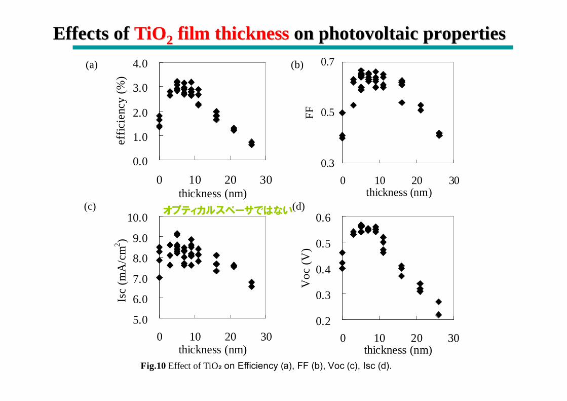
Fig.10 Effect of TiO₂ on Efficiency (a), FF (b), Voc (c), Isc (d).
(a) (b)
(c) (d)
Effects of Effects of TiOTiO22 film thicknessfilm thickness on photovoltaic propertieson photovoltaic properties
0.0
1.0
2.0
3.0
4.0
0 10 20 30thickness (nm)
effic
ienc
y (%
)
0.3
0.5
0.7
0 10 20 30thickness (nm)
FF0.2
0.3
0.4
0.5
0.6
0 10 20 30thickness (nm)
Voc
(V)
5.0
6.0
7.0
8.0
9.0
10.0
0 10 20 30thickness (nm)
Isc
(mA
/cm
2 )
オプティカルスペーサではない
s
T
oc
T
prev
psj R
VV
VRjR
RjV
≈=∂∂
=
exp10
+
+
pps
T
ssc
T
prev
psV RRR
VRj
VRj
RR
jV
≈≈−
=∂∂
= +
+
+
)exp(10
100100max ×⋅⋅
=×=light
scoc
light PFFJV
PP
η
scocscoc JVJV
JVPFF
⋅⋅
=⋅
= maxmaxmax
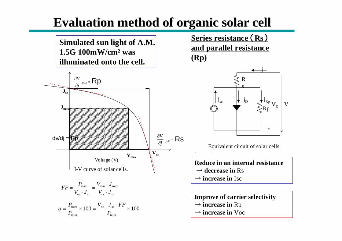
I-V curve of solar cells.
Simulated sun light of A.M. 1.5G 100mW/cm² was illuminated onto the cell.
Voltage (V)Vmax
Voc
Jmax
Jsc
Rs
jsc
j
jD VVD
jRp
Equivalent circuit of solar cells.
Series resistance (Rs)and parallel resistance (Rp)
Evaluation method of organic solar cellEvaluation method of organic solar cell
Rp
dv/dj = Rp
Rp
Rs
Reduce in an internal resistance → decrease in Rs→ increase in Isc
Improve of carrier selectivity → increase in Rp→ increase in Voc
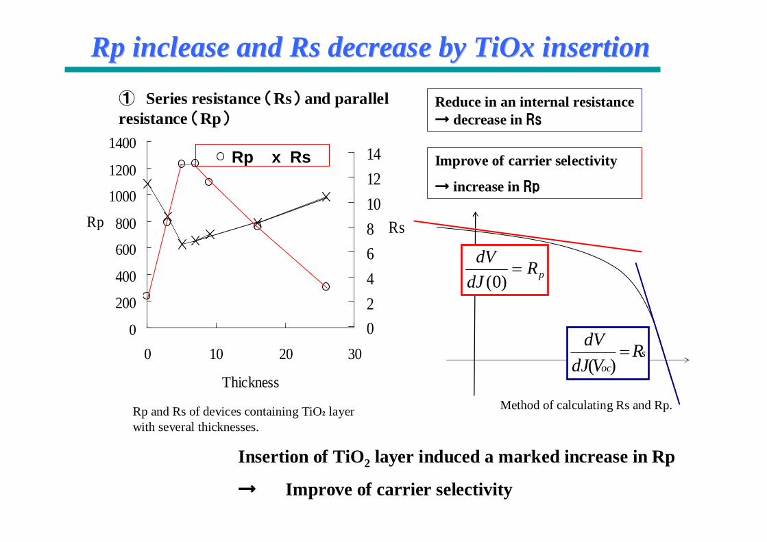
Improve of carrier selectivity
→ increase in Rp
Reduce in an internal resistance → decrease in Rs
Insertion of TiO2 layer induced a marked increase in Rp
→ Improve of carrier selectivity
① Series resistance (Rs) and parallel resistance (Rp)
Rp and Rs of devices containing TiO₂ layer with several thicknesses.
soc
RVdJ
dV=
)(
pRdJ
dV=
)0(
Method of calculating Rs and Rp.
RpRp incleaseinclease and and RsRs decrease by decrease by TiOxTiOx insertioninsertion
Rp x Rs
0
200
400
600
800
1000
1200
1400
0 10 20 30
Thickness
Rp
02468101214
Rs
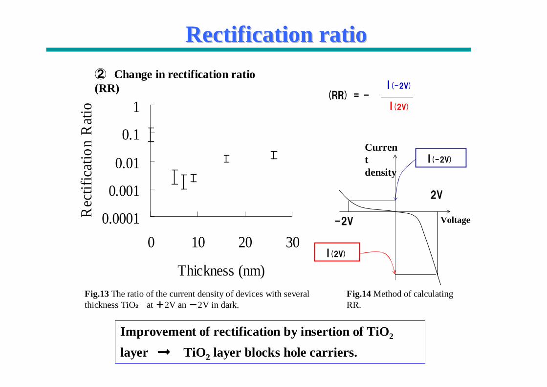
2V
-2V Voltage
Current density
I(-2V)
I(2V)
(RR) = -I(-2V)
I(2V)
Improvement of rectification by insertion of TiO2
layer → TiO2 layer blocks hole carriers.
② Change in rectification ratio (RR)
Fig.13 The ratio of the current density of devices with several thickness TiO₂ at +2V an -2V in dark.
0.0001
0.001
0.01
0.1
1
0 10 20 30
Thickness (nm)
Rec
tific
atio
n R
atio
Fig.14 Method of calculating RR.
Rectification ratioRectification ratio
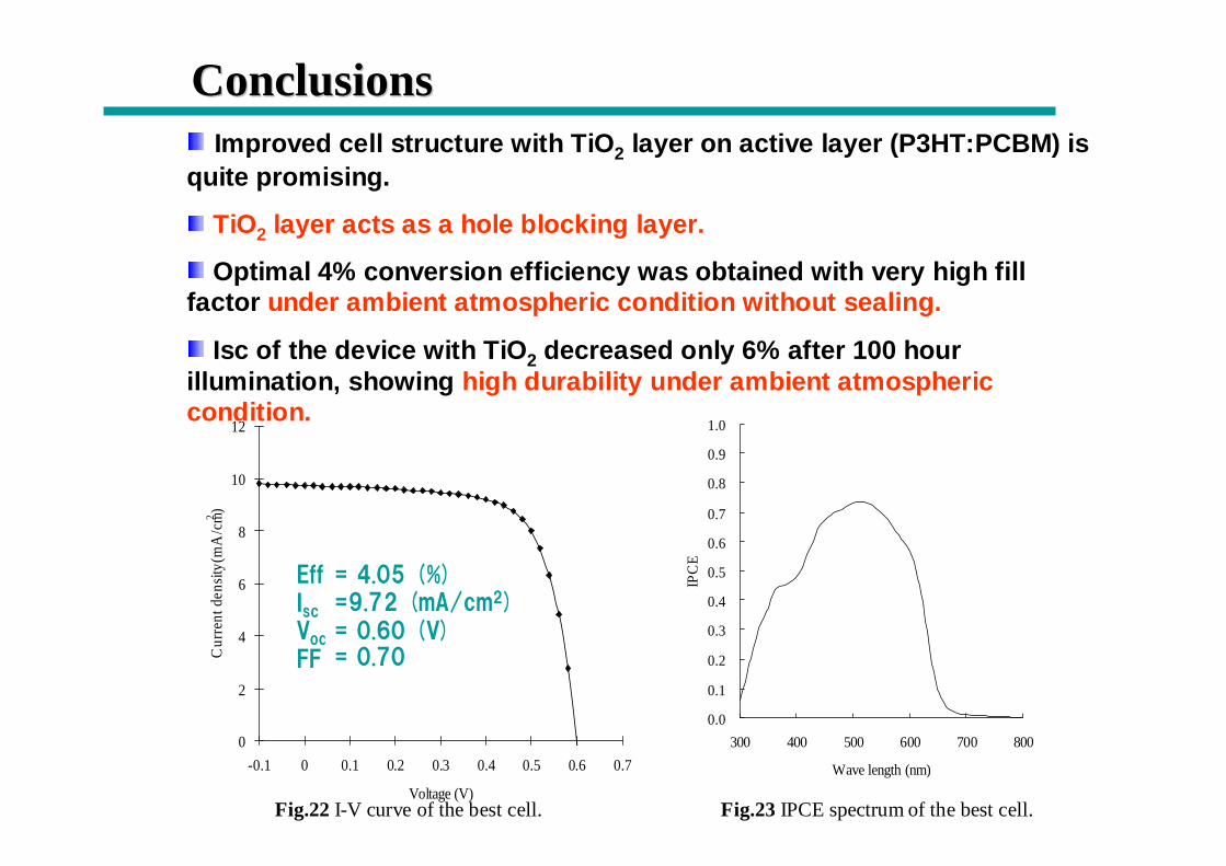
Improved cell structure with TiO2 layer on active layer (P3HT:PCBM) is quite promising.
TiO2 layer acts as a hole blocking layer.
Optimal 4% conversion efficiency was obtained with very high fill factor under ambient atmospheric condition without sealing.
Isc of the device with TiO2 decreased only 6% after 100 hour illumination, showing high durability under ambient atmospheric condition.
0.0
0.1
0.2
0.3
0.4
0.5
0.6
0.7
0.8
0.9
1.0
300 400 500 600 700 800
Wave length (nm)
IPC
E
0
2
4
6
8
10
12
-0.1 0 0.1 0.2 0.3 0.4 0.5 0.6 0.7
Voltage (V)
Cur
rent
den
sity(
mA
/cm2 )
EffIsc
Voc
FF
= 4.05 (%)=9.72 (mA/cm2)= 0.60 (V)= 0.70
Fig.22 I-V curve of the best cell. Fig.23 IPCE spectrum of the best cell.
Conclusions Conclusions
Organic Thin Film solar Cell
□ Preparation of hole transport layer (HTL) using PEDOT:PSS polymer brash
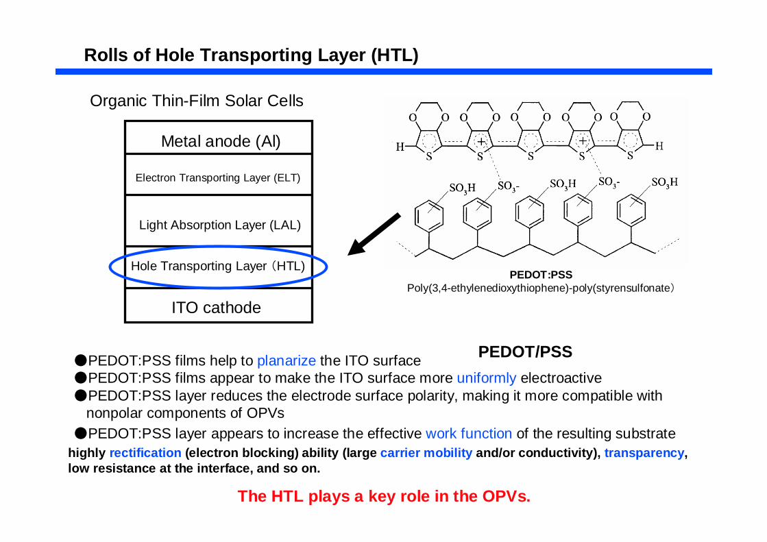
Rolls of Hole Transporting Layer (HTL)
PEDOT/PSS
Organic Thin-Film Solar Cells
●PEDOT:PSS films help to planarize the ITO surface●PEDOT:PSS films appear to make the ITO surface more uniformly electroactive●PEDOT:PSS layer reduces the electrode surface polarity, making it more compatible with
nonpolar components of OPVs●PEDOT:PSS layer appears to increase the effective work function of the resulting substrate
ITO cathode
Metal anode (Al)
Hole Transporting Layer (HTL)
Electron Transporting Layer (ELT)
Light Absorption Layer (LAL)
The HTL plays a key role in the OPVs.
highly rectification (electron blocking) ability (large carrier mobility and/or conductivity), transparency, low resistance at the interface, and so on.
PEDOT:PSSPoly(3,4-ethylenedioxythiophene)-poly(styrensulfonate)
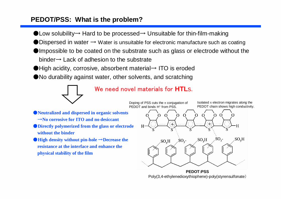
●Low solubility→ Hard to be processed→ Unsuitable for thin-film-making●Dispersed in water → Water is unsuitable for electronic manufacture such as coating●Impossible to be coated on the substrate such as glass or electrode without the
binder→ Lack of adhesion to the substrate●High acidity, corrosive, absorbent material→ ITO is eroded●No durability against water, other solvents, and scratching
●Neutralized and dispersed in organic solvents →No corrosive for ITO and no desiccant
●Directly polymerized from the glass or electrode without the binder
●High density without pin-hole →Decrease the resistance at the interface and enhance the physical stability of the film
We need novel materials for HTLs.
PEDOT/PSS: What is the problem?
Doping of PSS cuts the π conjugation of PEDOT and binds H+ from PSS.
Isolated π electron migrates along the PEDOT chain shows high conductivity.
PEDOT:PSSPoly(3,4-ethylenedioxythiophene)-poly(styrensulfonate)
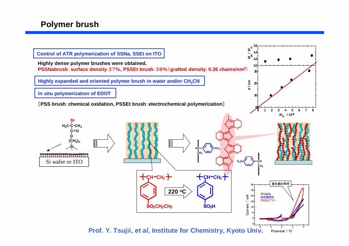
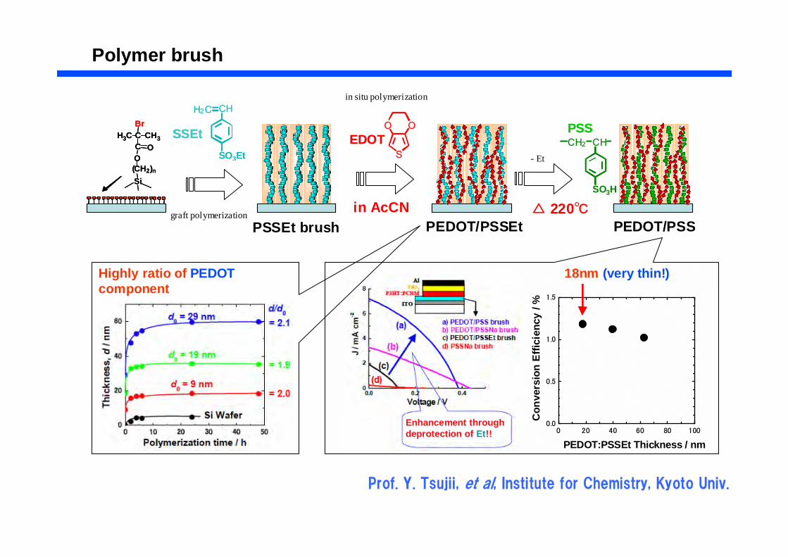
Polymer brush
[PSS brush:chemical oxidation, PSSEt brush:electrochemical polymerization]
Si wafer or ITO
C OC
O(CH2)nSi
H3C CH3
Br
CHCH2
O3S
HCCH2
SO3
SO
O
SO
O
S
O
O
SO
O
-2 -1 0 1 25
0
-5
-10
-15
-20
-25
-30
Curr
ent
/ m
A
Potential / V)
ITOのみBHE固定化PSSEtブラシ
重合膜の形成
Control of ATR polymerization of SSNa, SSEt on ITO
Highly dense polymer brushes were obtained.PSSNabrush:surface density 37%, PSSEt brush:38%(grafted density:0.26 chains/nm2)
Highly expanded and oriented polymer brush in water and/or CH3CN
In situ polymerization of EDOT
220 oC
0 1 2 3 4 5 6 7 80
10
20
30
d/ n
m
Mn / 104
1.0
1.2
1.4
1.6
M w/M
n
Prof. Y. Tsujii, et al, Institute for Chemistry, Kyoto Univ.
C OC
O(CH2)nSi
H3C CH3
Br
C OC
O(CH2)nSi
H3C CH3
BrSSEtSSEt
CHH2C
SO3Et
①① グラフト重合グラフト重合 ②②inin--situsitu重合重合
EDOTEDOTOO
S
③脱保護③脱保護
in AcCN △ 220℃
CHCH2
SO3H
PSSEt brush PEDOT/PSSEt PEDOT/PSS
PSSPSS
Highly ratio of PEDOTcomponent
0 20 40 60 80 1000.0
0.5
1.0
1.5
PEDOT:PSSEt Thickness / nm
Con
vers
ion
Effic
ienc
y / %
18nm (very thin!)
graft polymerization
in situ polymerization
- Et
Polymer brush
Enhancement through deprotection of Et!!
Prof. Y. Tsujii, et al, Institute for Chemistry, Kyoto Univ.
Hybrid solar Cell
□ Consept of supra-hierarchical nano-structured cell
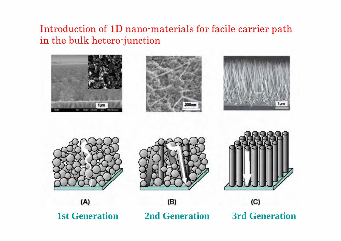
1st Generation 2nd Generation 3rd Generation
Introduction of 1D nano-materials for facile carrier path in the bulk hetero-junction
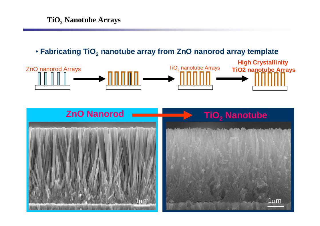
TiO2 Nanotube Arrays
ZnO nanorod Arrays TiO2 nanotube Arrays
• Fabricating TiO2 nanotube array from ZnO nanorod array templateHigh Crystallinity
TiO2 nanotube Arrays
1μm1μm
ZnO Nanorod TiO2 Nanotube
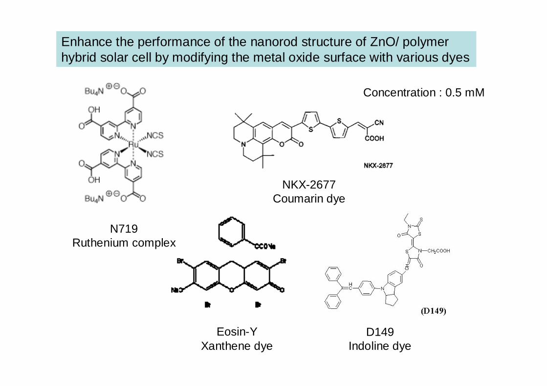
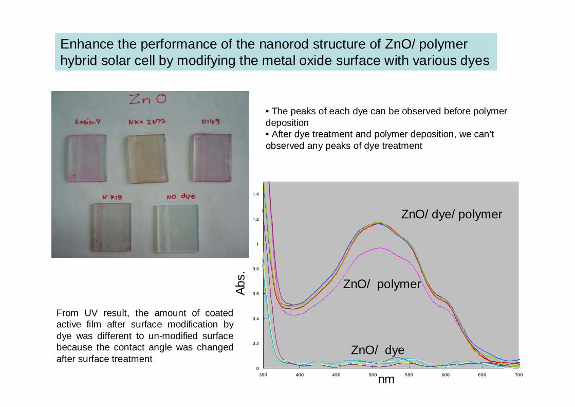
Enhance the performance of the nanorod structure of ZnO/ polymer hybrid solar cell by modifying the metal oxide surface with various dyes
N719Ruthenium complex
NKX-2677Coumarin dye
D149Indoline dye
Eosin-YXanthene dye
Concentration : 0.5 mM
0
0.2
0.4
0.6
0.8
1
1.2
1.4
350 400 450 500 550 600 650 700nm
Abs.
Enhance the performance of the nanorod structure of ZnO/ polymer hybrid solar cell by modifying the metal oxide surface with various dyes
• The peaks of each dye can be observed before polymer deposition• After dye treatment and polymer deposition, we can’t observed any peaks of dye treatment
ZnO/ dye/ polymer
ZnO/ polymer
ZnO/ dye
From UV result, the amount of coated active film after surface modification by dye was different to un-modified surface because the contact angle was changed after surface treatment
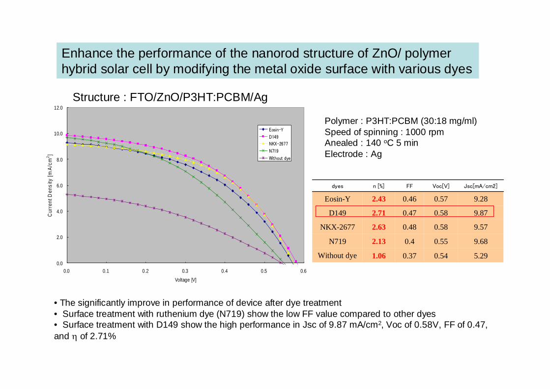
Enhance the performance of the nanorod structure of ZnO/ polymer hybrid solar cell by modifying the metal oxide surface with various dyes
0.0
2.0
4.0
6.0
8.0
10.0
12.0
0.0 0.1 0.2 0.3 0.4 0.5 0.6
Voltage [V]
Cur
rent
Den
sity
[mA/
cm2 ]
Eosin-Y
D149
NKX-2677
N719
Without dye
• The significantly improve in performance of device after dye treatment • Surface treatment with ruthenium dye (N719) show the low FF value compared to other dyes• Surface treatment with D149 show the high performance in Jsc of 9.87 mA/cm2, Voc of 0.58V, FF of 0.47, and η of 2.71%
5.29 0.54 0.37 1.06Without dye
9.680.550.42.13N719
9.570.580.482.63NKX-2677
9.870.580.472.71D149
9.280.570.462.43Eosin-Y
Jsc[mA/cm2]Voc[V]FFn [%]dyes
Polymer : P3HT:PCBM (30:18 mg/ml)Speed of spinning : 1000 rpmAnealed : 140 oC 5 minElectrode : Ag
Structure : FTO/ZnO/P3HT:PCBM/Ag
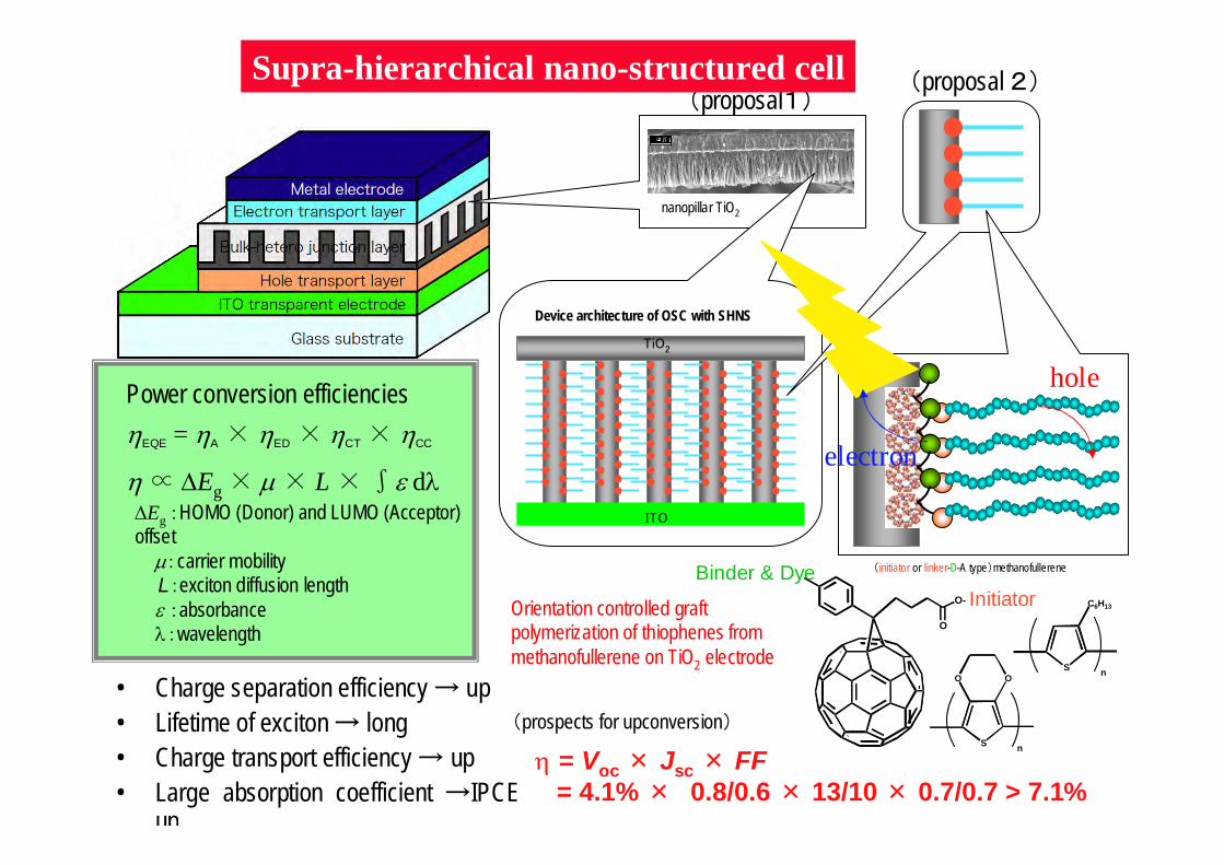
Orientation controlled graft polymerization of thiophenes from methanofullerene on TiO2 electrode
(initiator or linker-D-A type)methanofullerene
nanopillar TiO2
Assembly of OSC with Supra-Hierarchical Nano-Structure
O-
O
Binder & DyeInitiator
TiO2
ITO
hole
electron
S
C6H13
n
S
OO
n
(proposal1)(proposal 2)
(prospects for upconversion)
η = Voc × Jsc × FF = 4.1% × 0.8/0.6 × 13/10 × 0.7/0.7 > 7.1%
• Charge separation efficiency → up• Lifetime of exciton → long• Charge transport efficiency → up• Large absorption coefficient →IPCE
up
Power conversion efficiencies
ΔEg :HOMO (Donor) and LUMO (Acceptor) offset μ:carrier mobility
L:exciton diffusion length ε :absorbance λ:wavelength
η ∝ ΔEg × μ × L ×∫ε dλ
ηEQE = ηA × ηED × ηCT × ηCC
Device architecture of OSC with SHNS
Supra-hierarchical nano-structured cell
New MaterialEntering
Battery Back-up
/7 Yen/kWh
2002 2007 2010 2020 2030
Very-Thin Cell/Multi-junction
14 Yen/kWh
Elec
tric
ity C
ost
50 Yen/kWh
Bulk Si &Thin Film Si/ Compound
Active Grid Control
23 Yen/kWh
30 Yen/kWh
New MaterialEntering
Battery Back-up
/7 Yen/kWh
2002 2007 2010 2020 2030
Very-Thin Cell/Multi-junction
14 Yen/kWh
Elec
tric
ity C
ost
50 Yen/kWh50 Yen/kWh
Bulk Si &Thin Film Si/ Compound
Active Grid Control
23 Yen/kWh
30 Yen/kWh30 Yen/kWh
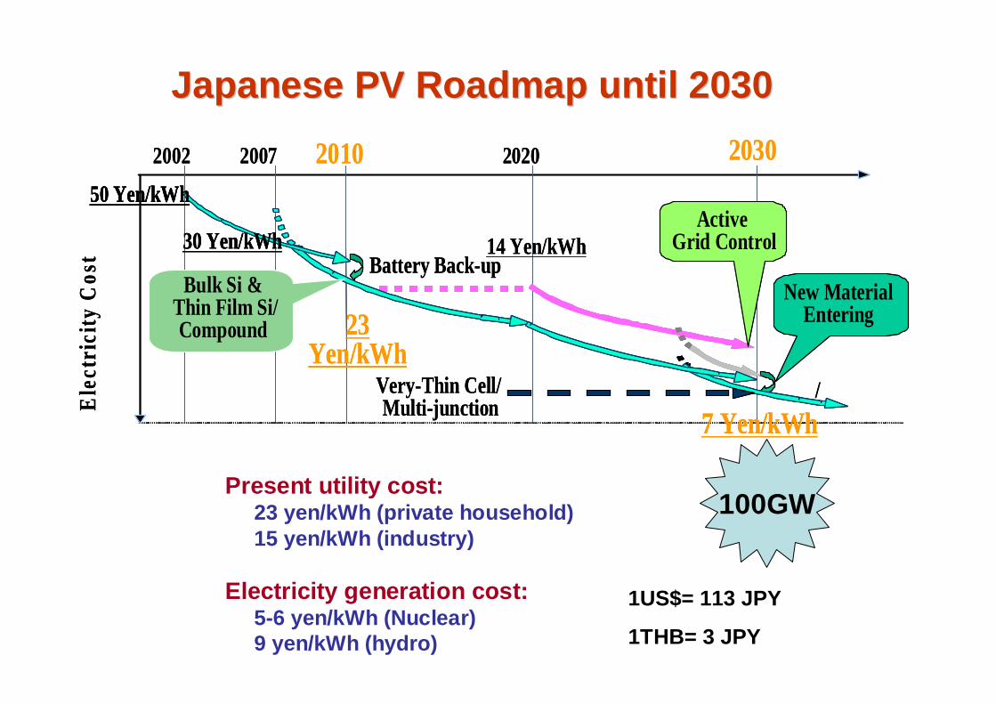
Japanese PV Roadmap until 2030Japanese PV Roadmap until 2030
Present utility cost:23 yen/kWh (private household)15 yen/kWh (industry)
Electricity generation cost:5-6 yen/kWh (Nuclear)9 yen/kWh (hydro)
100GW
1US$= 113 JPY
1THB= 3 JPY
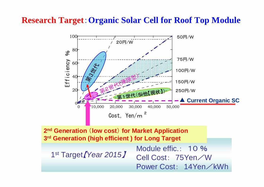
Research Target:Organic Solar Cell for Roof Top Module
100
80
60
40
20
0
Efficiency %
50,00040,00030,00020,00010,0000
Cost,Yen/m2
100円/W
150円/W
75円/W
20円/W50円/W
250円/W
Current Organic SC第1世代(Si他【現状】)
2nd Generation (low cost) for Market Application3rd Generation (high efficient ) for Long Target
1st Target【Year 2015】Module effic.: 10 %Cell Cost: 75Yen/WPower Cost: 14Yen/kWh
第2世代(薄膜型)
第3
世代