subharmonic mixers in cmos microwave integrated · pdf filesubharmonic mixers in cmos...
TRANSCRIPT

Subharmonic Mixers in CMOS
Microwave Integrated Circuits
by
Bradley Richard Jackson
A thesis submitted to the
Department of Electrical and Computer Engineering
in conformity with the requirements for
the degree of Doctor of Philosophy
Queen’s University
Kingston, Ontario, Canada
March 2009
Copyright c© Bradley Richard Jackson, 2009

Abstract
This thesis explores the design and applications of subharmonic mixers in CMOS
microwave integrated circuits. First, a 2× down-converting subharmonic mixer is
demonstrated with a measured conversion gain of 8 dB using a 2.1 GHz RF signal.
Extending the concept of the 2× subharmonic mixer, a 4× subharmonic mixer is pro-
posed that operates in the 12 GHz Ku-band. This circuit is the first 4× subharmonic
mixer in CMOS, and achieves a 6 dB conversion gain, which is the highest for any
4× subharmonic mixer regardless of circuit topology or fabrication technology. Fur-
thermore, it achieves very high measured isolation between its ports (e.g. 4LO–RF :
59 dB).
Since both the 2× and the 4× subharmonic mixers require a quadrature oscil-
lator, a new oscillator circuit is presented that could be used with either of the
aforementioned mixers. This quadrature oscillator uses active superharmonic cou-
pling to establish the quadrature fundamental relationship. The oscillation frequency
is 3.0 GHz and the measured output power is −6 dBm.
A dual-band mixer/oscillator is also demonstrated that can operate as either a
fundamental mixer or a subharmonic mixer depending on a control voltage. This
circuit operates from 5.0 GHz to 6.0 GHz or from 9.8 GHz to 11.8 GHz by using
either the fundamental output or the second harmonic output of the quadrature
i

oscillator circuit described above and achieves conversion gain over both frequency
bands.
A novel frequency tripler circuit is presented based on a subharmonic mixer. This
circuit uses the 2× subharmonic mixer discussed above, along with a feedforward
fundamental cancellation circuit. The measured fundamental suppression is up to
30 dB and the conversion gain is up to 3 dB. Finally, a frequency divider circuit
based on a subharmonic mixer is presented that divides the input signal frequency by
a factor of three. This circuit uses a single-balanced version of the 2× subharmonic
mixer described above in a regenerative divider topology. The measured input signal
bandwidth is 300 MHz (5.2 GHz to 5.5 GHz) with an input power of −7 dBm and
the maximum conversion gain is 0 dB.
ii

Acknowledgments
There are many people that I would like to thank for their generous support and
encouragement throughout the course of my Ph.D. studies. First, I would like to
thank my supervisor, Dr. Carlos Saavedra, for his guidance over the past five years
throughout both my Master’s and my Ph.D. degrees. He has continually provided
me with advice, encouragement, and the opportunities to improve my research and
engineering skills.
I would also like to thank several students from the lab for their generous assistance
with my research-related problems and for being good partners in our frequent tennis
matches. First, and foremost I would like to thank Denis Zheng for his never-ending
willingness to give his time over the five years we spent together in the lab. Much
assistance and many useful discussions regarding the designs and measurements in
this thesis were also provided by Gideon Yong, Stanley Ho, Ahmed El-Gabaly, and
John Carr.
The integrated circuits fabricated for this thesis would not be possible without the
support and IC grants provided by CMC. I would specifically like to thank Mariusz
Jarosz, Patricia Greig, Jim Quinn, and Feng Liu of CMC, for offering technical assis-
tance and equipment that was used for testing the chips in this thesis. Furthermore,
many of the measurements performed in this thesis made use of Dr. Brian Frank’s
iii

equipment that he generously shared. Thanks also go to several ECE staff members
including Greg McLeod for perpetually fixing our Unix server problem du jour, and
Debie Fraser & Bernice Ison for always being very friendly and helpful when any
administrative issues arose.
My family has been very understanding and supportive over the course of my post-
graduate education. In particular, I would like to thank my Mom & Dad, and my
Grandfather, as well as the rest of my family: Michelle & Wade, Keagan & Makayla,
Sylvia & Bob, Tom, Diane & Gary, Lyn & Dustin, and Jacob & Ava (also Abby for
reminding me to relax and not take things too seriously).
Without question, the person that was the most crucial to the completion of this
degree was my wife, Elisabeth. From initially encouraging me to start my graduate
studies to the completion of this thesis she has been a constant source of motivation
and support, and for that I will always be grateful.
iv

Table of Contents
Abstract i
Acknowledgements iii
Table of Contents v
List of Figures ix
List of Tables xiv
List of Abbreviations and Symbols xv
Chapter 1: Introduction . . . . . . . . . . . . . . . . . . . . . . . . . 1
1.1 Motivation . . . . . . . . . . . . . . . . . . . . . . . . . . . . . . . . . 1
1.2 Microwave Integrated Circuits in CMOS . . . . . . . . . . . . . . . . 3
1.3 Thesis Overview . . . . . . . . . . . . . . . . . . . . . . . . . . . . . . 5
1.4 Contributions . . . . . . . . . . . . . . . . . . . . . . . . . . . . . . . 8
Chapter 2: Literature Review . . . . . . . . . . . . . . . . . . . . . 10
2.1 Mixer Background . . . . . . . . . . . . . . . . . . . . . . . . . . . . 10
2.1.1 Fundamental Mixers . . . . . . . . . . . . . . . . . . . . . . . 10
2.1.2 Subharmonic Mixers . . . . . . . . . . . . . . . . . . . . . . . 12
v

2.2 Wireless Communication System Architecture . . . . . . . . . . . . . 16
2.2.1 Superheterodyne . . . . . . . . . . . . . . . . . . . . . . . . . 16
2.2.2 Direct-Conversion . . . . . . . . . . . . . . . . . . . . . . . . . 18
2.3 Mixer Circuit Review . . . . . . . . . . . . . . . . . . . . . . . . . . . 21
2.3.1 Fundamental Mixers . . . . . . . . . . . . . . . . . . . . . . . 21
2.3.2 Subharmonic Mixers . . . . . . . . . . . . . . . . . . . . . . . 26
2.4 Oscillators Circuit Review . . . . . . . . . . . . . . . . . . . . . . . . 36
2.4.1 Resonators for CMOS Microwave Oscillators . . . . . . . . . . 36
2.4.2 Common Oscillator Topologies . . . . . . . . . . . . . . . . . . 38
2.5 Frequency Multiplier Circuit Review . . . . . . . . . . . . . . . . . . 45
2.5.1 Common Frequency Multiplier Topologies . . . . . . . . . . . 46
2.6 Frequency Divider Circuit Review . . . . . . . . . . . . . . . . . . . . 51
2.6.1 Common Frequency Divider Topologies . . . . . . . . . . . . . 52
Chapter 3: A 2x Subharmonic Mixer in CMOS . . . . . . . . . . . 57
3.1 Introduction . . . . . . . . . . . . . . . . . . . . . . . . . . . . . . . . 57
3.2 Concept of the 2x Subharmonic Mixer . . . . . . . . . . . . . . . . . 58
3.3 Circuit Design . . . . . . . . . . . . . . . . . . . . . . . . . . . . . . . 59
3.3.1 Subharmonic Mixer Core . . . . . . . . . . . . . . . . . . . . . 59
3.3.2 RF and LO Input Baluns . . . . . . . . . . . . . . . . . . . . 66
3.3.3 Output Balun . . . . . . . . . . . . . . . . . . . . . . . . . . . 71
3.3.4 Complete Circuit . . . . . . . . . . . . . . . . . . . . . . . . . 72
3.4 Measurement Results . . . . . . . . . . . . . . . . . . . . . . . . . . . 73
3.5 Summary . . . . . . . . . . . . . . . . . . . . . . . . . . . . . . . . . 79
vi

Chapter 4: A CMOS Ku-Band 4x Subharmonic Mixer . . . . . . . 81
4.1 Introduction . . . . . . . . . . . . . . . . . . . . . . . . . . . . . . . . 81
4.2 Concept of the 4x Subharmonic Mixer . . . . . . . . . . . . . . . . . 82
4.3 Circuit Design . . . . . . . . . . . . . . . . . . . . . . . . . . . . . . . 84
4.3.1 Mixer Core . . . . . . . . . . . . . . . . . . . . . . . . . . . . 84
4.3.2 Input RF Balun . . . . . . . . . . . . . . . . . . . . . . . . . . 88
4.3.3 LO Phase Shifters . . . . . . . . . . . . . . . . . . . . . . . . . 90
4.3.4 Output Balun . . . . . . . . . . . . . . . . . . . . . . . . . . . 92
4.4 Measurement Results . . . . . . . . . . . . . . . . . . . . . . . . . . . 93
4.5 Summary . . . . . . . . . . . . . . . . . . . . . . . . . . . . . . . . . 101
Chapter 5: Quadrature Oscillator . . . . . . . . . . . . . . . . . . . 103
5.1 Introduction . . . . . . . . . . . . . . . . . . . . . . . . . . . . . . . . 103
5.2 Concept of the Quadrature Oscillator . . . . . . . . . . . . . . . . . . 104
5.3 Circuit Design . . . . . . . . . . . . . . . . . . . . . . . . . . . . . . . 105
5.4 Measurement Results . . . . . . . . . . . . . . . . . . . . . . . . . . . 108
5.5 Summary . . . . . . . . . . . . . . . . . . . . . . . . . . . . . . . . . 112
Chapter 6: A Dual-Band Mixer/Oscillator . . . . . . . . . . . . . . 114
6.1 Introduction . . . . . . . . . . . . . . . . . . . . . . . . . . . . . . . . 114
6.2 Concept of the Dual-Band Mixer/Oscillator . . . . . . . . . . . . . . 115
6.3 Circuit Design . . . . . . . . . . . . . . . . . . . . . . . . . . . . . . . 116
6.3.1 Voltage-Controlled Quadrature Oscillator . . . . . . . . . . . . 117
6.3.2 Mixer . . . . . . . . . . . . . . . . . . . . . . . . . . . . . . . 119
6.4 Measurement Results . . . . . . . . . . . . . . . . . . . . . . . . . . . 123
vii

6.5 Summary . . . . . . . . . . . . . . . . . . . . . . . . . . . . . . . . . 129
Chapter 7: A Frequency Tripler Using a Subharmonic Mixer . . . 131
7.1 Introduction . . . . . . . . . . . . . . . . . . . . . . . . . . . . . . . . 131
7.2 Concept of the Frequency Tripler . . . . . . . . . . . . . . . . . . . . 132
7.3 Circuit Design . . . . . . . . . . . . . . . . . . . . . . . . . . . . . . . 133
7.3.1 Subharmonic Mixer . . . . . . . . . . . . . . . . . . . . . . . . 133
7.3.2 Fundamental Feedforward Circuit . . . . . . . . . . . . . . . . 135
7.3.3 Fundamental Cancellation Circuit . . . . . . . . . . . . . . . . 137
7.4 Measurement Results . . . . . . . . . . . . . . . . . . . . . . . . . . . 140
7.5 Summary . . . . . . . . . . . . . . . . . . . . . . . . . . . . . . . . . 148
Chapter 8: A Frequency Divider Using a Subharmonic Mixer . . 149
8.1 Introduction . . . . . . . . . . . . . . . . . . . . . . . . . . . . . . . . 149
8.2 Concept of the Frequency Divider . . . . . . . . . . . . . . . . . . . . 150
8.3 Circuit Design . . . . . . . . . . . . . . . . . . . . . . . . . . . . . . . 152
8.4 Measurement Results . . . . . . . . . . . . . . . . . . . . . . . . . . . 155
8.5 Summary . . . . . . . . . . . . . . . . . . . . . . . . . . . . . . . . . 159
Chapter 9: Summary and Conclusions . . . . . . . . . . . . . . . . 161
9.1 Summary . . . . . . . . . . . . . . . . . . . . . . . . . . . . . . . . . 161
9.2 Review of Contributions . . . . . . . . . . . . . . . . . . . . . . . . . 164
9.3 Future Work . . . . . . . . . . . . . . . . . . . . . . . . . . . . . . . . 166
References . . . . . . . . . . . . . . . . . . . . . . . . . . . . . . . . . . 168
viii

List of Figures
2.1 Fundamental mixer block diagram. . . . . . . . . . . . . . . . . . . . 11
2.2 Subharmonic mixer block diagram. . . . . . . . . . . . . . . . . . . . 13
2.3 Anti-parallel diode pair conceptual circuit. . . . . . . . . . . . . . . . 14
2.4 Block diagram of a superheterodyne receiver. . . . . . . . . . . . . . . 17
2.5 Block diagram of a direct-conversion receiver. . . . . . . . . . . . . . 19
2.6 Potential LO self-mixing paths. . . . . . . . . . . . . . . . . . . . . . 20
2.7 Gilbert-cell mixer. . . . . . . . . . . . . . . . . . . . . . . . . . . . . . 22
2.8 Resistive FET mixer. . . . . . . . . . . . . . . . . . . . . . . . . . . . 25
2.9 Basic 2× subharmonic mixer circuit used in [25, 28, 31, 35]. . . . . . 27
2.10 Subharmonic mixer circuit proposed in [36]. . . . . . . . . . . . . . . 30
2.11 Passive FET subharmonic mixer. . . . . . . . . . . . . . . . . . . . . 31
2.12 Subharmonic mixer using an anti-parallel diode-pair. . . . . . . . . . 33
2.13 Common model used for CMOS inductors. . . . . . . . . . . . . . . . 38
2.14 Colpitts oscillator circuit. . . . . . . . . . . . . . . . . . . . . . . . . . 39
2.15 Negative resistance generated from cross-coupled FETs. . . . . . . . . 40
2.16 Cross-coupled FET oscillator. . . . . . . . . . . . . . . . . . . . . . . 41
2.17 Complementary cross-coupled FET oscillator. . . . . . . . . . . . . . 42
2.18 Quadrature oscillator superharmonic coupling techniques. . . . . . . . 44
2.19 Simplified frequency doubler using FET non-linearities. . . . . . . . . 47
ix

2.20 Simplified circuit of an injection-locked frequency doubler. . . . . . . 48
2.21 Push-push frequency doubler circuit. . . . . . . . . . . . . . . . . . . 49
2.22 Simplified circuit of a regenerative frequency divider. . . . . . . . . . 53
2.23 Simplified circuit of an injection-locked frequency divider. . . . . . . . 55
3.1 Block diagram of the proposed 2× subharmonic mixer . . . . . . . . . 58
3.2 Proposed CMOS 2× subharmonic mixer core. . . . . . . . . . . . . . 60
3.3 LO frequency doubling in the 2× subharmonic mixer. . . . . . . . . . 60
3.4 LO transistor modeling for the 2× subharmonic mixer . . . . . . . . 62
3.5 Calculated and simulated conversion gain of the 2× SHM. . . . . . . 65
3.6 Single FET balun circuit. . . . . . . . . . . . . . . . . . . . . . . . . . 66
3.7 Differential pair balun circuit. . . . . . . . . . . . . . . . . . . . . . . 68
3.8 Common-gate, common-source balun circuit. . . . . . . . . . . . . . . 68
3.9 Simulated 2× SHM active balun performance. . . . . . . . . . . . . . 70
3.10 LO input balun and phase shifters for the 2× SHM. . . . . . . . . . . 71
3.11 Output balun and buffer for the 2× SHM. . . . . . . . . . . . . . . . 72
3.12 Photograph of fabricated CMOS 2× subharmonic mixer. . . . . . . . 73
3.13 Measured and simulated P1dB for the 2× SHM . . . . . . . . . . . . . 75
3.14 Conversion gain at various LO power levels for the 2× SHM. . . . . . 75
3.15 Measured RF input reflection coefficient for the 2× SHM. . . . . . . . 77
3.16 Measured LO input reflection coefficient for the 2× SHM. . . . . . . . 77
3.17 Third-order intercept point measurement for the 2× SHM. . . . . . . 78
4.1 The mixer core of the proposed 4× SHM. . . . . . . . . . . . . . . . . 83
4.2 Modeling the 4× SHM LO generation circuit . . . . . . . . . . . . . . 85
4.3 RF active balun circuit for the 4× SHM. . . . . . . . . . . . . . . . . 89
x

4.4 45 phase shifter circuit for the 4× SHM. . . . . . . . . . . . . . . . . 91
4.5 90 RC–CR phase shifter used in the 4× SHM. . . . . . . . . . . . . 92
4.6 Output balun circuit for the 4× SHM. . . . . . . . . . . . . . . . . . 93
4.7 Measured 4× subharmonic mixer output spectrum . . . . . . . . . . . 94
4.8 Measured P1dB for the 4× SHM . . . . . . . . . . . . . . . . . . . . . 95
4.9 Conversion gain at various LO power levels for the 4× SHM. . . . . . 96
4.10 Measured IP3 for the 4× SHM . . . . . . . . . . . . . . . . . . . . . . 98
4.11 Measured IP2 for the 4× SHM . . . . . . . . . . . . . . . . . . . . . . 98
4.12 Measured RF input reflection coefficient for the 4× SHM. . . . . . . . 99
4.13 Microphotograph of the proposed 4× SHM. . . . . . . . . . . . . . . 102
5.1 Quadrature oscillator superharmonic coupling techniques. . . . . . . . 104
5.2 Proposed quadrature oscillator core circuit. . . . . . . . . . . . . . . . 106
5.3 Complete quadrature oscillator circuit. . . . . . . . . . . . . . . . . . 107
5.4 Time-domain measurement setup for the quadrature oscillator. . . . . 109
5.5 Measured time-domain quadrature oscillator output. . . . . . . . . . 109
5.6 Measured quadrature oscillator output spectrum. . . . . . . . . . . . 110
5.7 Measured phase noise of quadrature oscillator. . . . . . . . . . . . . . 111
5.8 Photograph of the proposed CMOS quadrature oscillator chip. . . . . 112
6.1 Block diagram of the proposed dual-band mixer/oscillator. . . . . . . 115
6.2 Quadrature VCO using superharmonic coupling. . . . . . . . . . . . . 118
6.3 Dual-band mixer/oscillator in subharmonic mode . . . . . . . . . . . 120
6.4 Circuit schematic of the proposed dual-band mixer/oscillator. . . . . 121
6.5 Measured fundamental LO frequency tuning range. . . . . . . . . . . 123
6.6 Measured conversion gain for dual-band mixer/oscillator . . . . . . . 125
xi

6.7 Measured dual-band mixer/oscillator 1-dB compression point. . . . . 125
6.8 Measured IP3 for the dual-band mixer/oscillator . . . . . . . . . . . . 127
6.9 Measured IP2 for the dual-band mixer/oscillator . . . . . . . . . . . . 127
6.10 Microphotograph of the fabricated dual-band mixer/oscillator . . . . 129
7.1 Block diagram of the proposed frequency tripler. . . . . . . . . . . . . 132
7.2 Core of the 2× SHM used in the frequency tripler. . . . . . . . . . . . 134
7.3 Generation of the frequency tripler quadrature LO signals. . . . . . . 135
7.4 Fundamental feedforward circuit used in the frequency tripler. . . . . 136
7.5 Tripler active balun, subtractor, and output buffer circuits. . . . . . . 138
7.6 Fundamental suppression calculation for the frequency tripler . . . . . 139
7.7 Measured frequency tripler output spectrum. . . . . . . . . . . . . . . 141
7.8 Measured tripler output power levels at various input powers. . . . . 142
7.9 Measured tripler output power tuned for optimal performance. . . . . 144
7.10 Simulated broadband performance of the tripler using an ideal quadra-
ture input signal with a power of −11 dBm. . . . . . . . . . . . . . . 145
7.11 Measured input and output phase noise for the frequency tripler. . . . 146
7.12 Microphotograph of the frequency tripler chip. . . . . . . . . . . . . . 147
8.1 Traditional Miller regenerative frequency divider. . . . . . . . . . . . 150
8.2 Block diagram of the proposed divide-by-three frequency divider. . . 151
8.3 Single-balanced 2× subharmonic mixer circuit. . . . . . . . . . . . . . 152
8.4 Tuned differential amplifier circuit. . . . . . . . . . . . . . . . . . . . 153
8.5 Simplified schematic of the proposed frequency divider (biasing not
shown). . . . . . . . . . . . . . . . . . . . . . . . . . . . . . . . . . . 154
8.6 Frequency divider output spectrum . . . . . . . . . . . . . . . . . . . 156
xii

8.7 Frequency divider conversion gain at various input frequencies . . . . 157
8.8 Frequency divider bandwidth . . . . . . . . . . . . . . . . . . . . . . 158
8.9 Frequency divider chip photograph. . . . . . . . . . . . . . . . . . . . 159
xiii

List of Tables
3.1 2× subharmonic mixer port-to-port isolation simulations. . . . . . . 78
3.2 2× subharmonic mixer circuit performance comparison. . . . . . . . 79
4.1 4× subharmonic mixer port-to-port isolation measurements. . . . . . 100
6.1 Dual-band mixer/oscillator LO feedthrough measurements. . . . . . . 128
7.1 Tripler circuit performance comparison . . . . . . . . . . . . . . . . . 147
xiv

List of Abbreviations and Symbols
Abbreviation Definition
SHM Subharmonic Mixer
CMOS Complimentary Metal-Oxide-Semiconductor
RF Radio Frequency
LO Local Oscillator
IF Intermediate Frequency
ADS Advanced Design System (software from Agilent)
LPF Low-Pass Filter
BPF Band-Pass Filter
ADC Analog-to-Digital Converter
CPW Coplanar waveguide
SAW Surface Acoustic Wave
SoC System-on-a-Chip
LNA Low-Noise Amplifier
VCO Voltage-Controlled Oscillator
RFC Radio Frequency Choke
IM2 Second-order intermodulation products
IM3 Third-order intermodulation products
xv

IIP2 Input-referred second-order intercept point
OIP2 Output-referred second-order intercept point
IIP3 Input-referred third-order intercept point
OIP3 Output-referred third-order intercept point
DSB Double Sideband (noise figure)
SSB Single Sideband (noise figure)
GSG Ground-Signal-Ground
P1dB 1-dB compression point
FET Field effect transistor
MOSFET Metal Oxide Semiconductor Field Effect Transistor
SiGe Silicon germanium
BiCMOS A process with both bipolar and CMOS transistors
GaAs Gallium arsenide
HEMT High Electron Mobility Transistor
InP Indium phosphide
RBW Resolution Bandwidth
VBW Video Bandwidth
f Frequency in Hz
ω Frequency in rad/s
fT , ωT Unity current gain frequency
fmax, ωmax Maximum frequency of oscillation
fRF , ωRF Frequency of the radio frequency signal
fLO, ωLO Frequency of the local oscillator signal
fIF , ωIF Frequency of the intermediate frequency signal
xvi

Q Quality factor
W Transistor gate width
L Transistor gate length
Esat Electric field where the electron velocity saturates
gm Transconductance
rg Series gate resistance
Cgs Parasitic gate-source capacitance
Cgd Parasitic gate-drain capacitance
µn Electron Mobility
Cox Gate oxide capacitance
Is Reverse-bias saturation current
Vt FET threshold voltage
Vth Diode thermal voltage
xvii

Chapter 1
Introduction
1.1 Motivation
Society’s demand for wireless communication devices that are faster and more robust
with increased functionality has been ongoing for decades and it is not likely that it
will subside anytime in the near future. In order to accommodate higher data-rate
systems and to avoid the increasingly cluttered frequency spectrum in the low-GHz
area, many new systems will need to move to higher frequencies where new challenges
in circuit design are encountered. To address this issue, new circuit topologies need to
be demonstrated that become increasingly advantageous as the frequency of operation
is increased. This is one motivation for the work in this dissertation.
In addition to the relentless desire to increase the performance of wireless commu-
nications systems, the desire to reduce costs is universal. The integrated circuit fabri-
cation technology used to realize almost all digital microprocessors is complementary
metal-oxide-semiconductor (CMOS) technology, which is very low-cost compared to
other fabrication technologies due to economies of scale. It is therefore very desirable
1

Chapter 1. Introduction 2
for the RF/microwave circuits in wireless communication devices to use CMOS tech-
nology in order to minimize costs. As such, all of the microwave integrated circuits
in this thesis use CMOS technology. Furthermore, if both the RF/microwave circuits
and the digital circuits use CMOS technology there is the potential for realizing a
complete system-on-a-chip (SoC), which can lead to increased functionality, further
cost reductions, and significant reductions in device size.
As discussed above, there are many advantages that can be gained if a system-
on-a-chip can be realized for a given application. Unfortunately, the most common
wireless receiver architecture (superheterodyne) contains components that are often
very difficult or impossible to integrate on the same chip as the microwave and digital
circuitry. To address this issue, there has been much interest of late in an alternative
wireless communication receiver architecture (direct-conversion) that does not require
the difficult-to-integrate components. Of course, new challenges are introduced with
this alternate architecture, and new circuits need to be investigated to address these
issues, which is another motivation for this work.
This dissertation predominantly focuses on an essential circuit used for wireless
communications, namely, the mixer, as well as the application of mixers in other
frequency conversion circuits. Mixers are fundamental circuit elements that are used
in both transmitters and receivers to convert signals in the frequency domain. In
general, mixers have three ports: a radio frequency (RF) port, a local oscillator
(LO) port, and an intermediate frequency (IF) port. In transmitters, they are used
for modulation and up-conversion to ease wireless transmission. Correspondingly,
in receivers, mixers are used for demodulation and down-conversion. In most cases,
mixers are realized by using the non-linearities in active devices or by using switches.

Chapter 1. Introduction 3
A specialized type of mixer, a subharmonic mixer (SHM), has unique advantages that
can address some of the issues discussed above regarding next-generation wireless
communication devices, and as such is the focus of this thesis.
1.2 Microwave Integrated Circuits in CMOS
Over the past 15 years there has been a tremendous amount of interest in the use of
CMOS technology for RF and microwave circuits (often referred to as RF CMOS).
As mentioned previously, there are significant benefits that can be derived from the
use of CMOS for RF circuits including the possibility of achieving the much heralded
system-on-a-chip. By combining the RF circuitry with the digital processing circuitry
on the same substrate, a significant cost savings can potentially be obtained. Since
the predominant technology used for digital circuitry is CMOS there is a natural
desire to use CMOS technology for RF circuits as well. In addition to system-on-a-
chip aspirations, it is also desirable to use CMOS for RF and microwave applications
because it is generally much less expensive than other technologies that have been
used in the past (e.g. GaAs). There are, however, significant challenges that are
encountered when using CMOS for RF circuits. Prior to the 1990s there was very little
work in the area of RF CMOS because the transistor could not attain the required
performance at high frequencies. The enormous advances in CMOS technology have
in large part been due to the geometrical scaling of the transistor. Two common
figures of merit for the high frequency performance of transistors are ωT and ωmax,
which are the frequencies at which the current and power gain, respectively, equal
unity and are given by [1]:

Chapter 1. Introduction 4
ωT =gm
Cgs + Cgd
(1.1)
ωmax =1
2
√ωT
rgCgd
(1.2)
where gm is the transconductance of the transistor, rg is the series gate resistance, and
Cgs and Cgd are the parasitic gate-source and gate-drain capacitances, respectively.
When the transistor is scaled, the parasitic capacitances decrease, which leads to an
increase in ωT and ωmax, and improved high frequency performance. For example, it
is currently possible to use CMOS technology to realize microwave mixers and low
noise amplifiers up to 60 GHz [2], and voltage controlled oscillators up to 192 GHz
[3]. Recently, a cutoff frequency of over 400 GHz was achieved using CMOS 45 nm
silicon-on-insulator (SOI) technology [4]. With this extremely high cutoff frequency,
it is expected that the applications of CMOS technology in the microwave/millimeter-
wave will continue to grow for some time into the future. For all of the circuits in
this thesis, either CMOS 0.18 µm or CMOS 0.13 µm technology was used. The cutoff
frequency, fT , for CMOS 0.18 µm is approximately 45 GHz and for CMOS 0.13 µm
it is approximately 105 GHz [5].
In addition to the high-frequency performance of the CMOS transistor, the other
major challenge to using CMOS for RF circuits is in regards to obtaining high quality
passive components, or more specifically, inductors. Inductors in RF CMOS circuits
are typically realized using a spiral. There are several metal layers available in any
modern CMOS technology and the inductors are generally fabricated on the top metal

Chapter 1. Introduction 5
layer. There are two primary reasons for this: (1) the top metal layer is generally
the thickest and thus has the lowest ohmic losses and (2) the relatively low resistiv-
ity of the silicon substrate causes serious parasitic effects, which can be reduced by
increasing the distance between the inductor and the substrate. At high frequencies
there can be significant capacitive coupling to the substrate and image currents pro-
duced that can seriously degrade an inductor’s performance. Furthermore, since these
structures can be relatively large in order to yield the desired value of inductance,
the inductor’s metal lines are correspondingly quite long and in many cases narrow,
which can cause significant ohmic losses. The combination of these parasitic effects
results in inductors with relatively low quality factors (Q-factors).
1.3 Thesis Overview
This thesis is organized topically by chapter. After a literature review, each chapter
explores a different application of subharmonic mixers in CMOS microwave integrated
circuits, with a summary in the final chapter.
A literature review is first presented in Chapter 2 that allows the contributions
of this thesis to be placed into a broader context. A brief discussion of the previous
work relevant to each of the circuits demonstrated in this thesis is presented.
Chapter 3 explores a 2× subharmonic mixer circuit using CMOS technology. This
circuit investigates the level of performance attainable and design issues with SHMs in
CMOS in preparation for designing a more advanced 4× subharmonic mixer circuit.
Included in this work is a circuit that generates a quadrature LO signal from a
single-ended LO input. Furthermore, an RF input active balun is used to generate a
differential RF signal from a single-ended input and an output active balun is used to

Chapter 1. Introduction 6
convert back to a single-ended signal for measurement. A conversion gain equation
for the mixer core circuit is derived and measurement results are shown.
Having verified the 2× subharmonic mixer topology in Chapter 3, the concept is
extended in Chapter 4 to realize a 4× subharmonic mixer that operates as a Ku-band
down-converter. This circuit requires octet-phase LO input signals, and as such, a
circuit is included on-chip to generate these signals from a differential LO input. An
RF input balun similar to the one used in Chapter 3 is implemented at a much higher
frequency (12.1 GHz as opposed to 2.1 GHz). A mathematical analysis of the mixer
is presented that explains how this circuit internally multiplies the frequency of the
LO signal by a factor of four.
Since the mixers presented in both Chapters 3 and 4 rely on a quadrature local
oscillator signal, Chapter 5 presents a compact quadrature oscillator that is suitable
for use with either mixer. This quadrature oscillator uses a technique called active
superharmonic coupling to enforce the quadrature fundamental relationship. Mea-
surement results are shown for the oscillator including output power spectrum, phase
noise, and quadrature accuracy.
Having explored subharmonic mixer circuits as well as an oscillator, Chapter 6
combines these circuits to realize a dual-band oscillator/mixer circuit for C-band and
X-band applications. The mixer operates using either the fundamental oscillator
output, or the second-harmonic output of the oscillator depending on the state of
a set of complementary switches. Therefore, this circuit can operate as either a
fundamental mixer, or a subharmonic mixer depending on a single control voltage.
In fundamental-mode, the circuit operates with RF input signals in C-band (5.0 GHz
to 6.0 GHz), and in subharmonic-mode the circuit operates with RF input signals in

Chapter 1. Introduction 7
X-band (9.8 GHz to 11.8 GHz). Measurement results are shown for both states of
the circuit.
In Chapter 7, a frequency multiplier is presented that uses a subharmonic mixer
to realize a frequency multiplication by three. Whereas most frequency multipliers
are even-ordered, a subharmonic mixer with the same input signal for the RF and
LO ports will produce an output signal that has a component at the fundamental
frequency and a component at three times the fundamental frequency. A feedforward
circuit is used to cancel the fundamental output of the subharmonic mixer, leaving
(ideally) only the tripled frequency component. Measurement results are shown that
indicate high-levels of fundamental suppression can be achieved using this technique
without a filter.
In Chapter 8, a frequency divider is demonstrated that divides the input signal
frequency by a factor of three using a single-balanced version of the 2× subharmonic
mixer described in Chapter 3. A regenerative frequency divider topology is used
with the 2× subharmonic mixer in CMOS 0.13 µm technology to realize a frequency
divider that accepts an input signal from 5.2 GHz to 5.5 GHz and outputs a signal
from 1.73 GHz to 1.83 GHz. Measurement results for this frequency divider are shown
including the output power spectrum as well as the bandwidth obtainable for different
input power levels.
Finally, a summary of the thesis is presented, as well as a review of the contribu-
tions made to the field of microwave integrated circuits through this work. The thesis
concludes with a discussion of potential directions for future work on subharmonic
mixers in microwave integrated circuits.

Chapter 1. Introduction 8
1.4 Contributions
The major contributions of this thesis are as follows:
The first 4× subharmonic mixer demonstrated in CMOS technology, and the
highest conversion gain for any 4× subharmonic mixer regardless of technique
or technology used. A measured conversion gain of 6 dB was achieved along
with very high isolation between ports, which demonstrates the potential of
high-order subharmonic mixers in CMOS technology. (Chapter 4) [6].
A unique frequency tripler circuit that uses a subharmonic mixer and fundamen-
tal cancellation to achieve conversion gain of 3 dB and fundamental suppression
of up to 30 dB without a filter (Chapter 7) [7].
The first 2× subharmonic mixer demonstrated in CMOS technology with mea-
sured results using the proposed topology, and one of the first CMOS subhar-
monic mixers overall. Active baluns were used for all ports to realize a compact
layout, and the measured conversion gain of 8 dB demonstrates the potential
for high conversion gain with this topology. (Chapter 3) [8].
The most compact quadrature oscillator using the superharmonic coupling tech-
nique and a phase noise of −116 dBc/Hz at a 1 MHz offset for a 3.0 GHz output
frequency, which is the lowest phase noise for a quadrature oscillator using active
superharmonic coupling (Chapter 5) [9].
A novel dual-band mixer/oscillator circuit that uses a single mixer core and a
single oscillator circuit for operation in both C-band and X-band. This circuit
Chapter 1. Introduction 9
achieves a conversion gain for RF input signals from 5.0 GHz to 6.0 GHz and
from 9.8 GHz to 11.8 GHz (Chapter 6) [10].
A novel frequency divider circuit that divides the input signal frequency by
a factor of three using a subharmonic mixer in a regenerative topology. This
circuit can achieve a conversion gain of up to 0 dB and an input signal bandwidth
of up to 430 MHz. Since the majority of frequency dividers are even-order (often
divide-by-two or four), the proposed odd-order divider circuit can add flexibility
to microwave circuit design (Chapter 8) [11].

Chapter 2
Literature Review
2.1 Mixer Background
This section will provide a brief background on both fundamental mixers and sub-
harmonic mixers in order to set the stage for a more detailed literature review of
previous mixer circuits.
2.1.1 Fundamental Mixers
By far the most common type of mixer is the fundamental-mode mixer. In this type
of mixer, the sum and difference of the two input frequencies are produced at the
output, as shown in Figure 2.1. Specifically, in the case of down-conversion, if fRF
and fLO are the two mixer input signal frequencies, then the IF output signal will
have frequency,
fIF = fRF − fLO (2.1)
10

Chapter 2. Literature Review 11
Figure 2.1: Fundamental mixer block diagram.
Alternatively, if the mixer is being used for up-conversion with fIF and fLO inputs,
the RF output signal will have frequency,
fRF = fIF + fLO (2.2)
In order to generate this frequency translation, a nonlinear device is required. A
straight-forward mathematical identity can illustrate how a nonlinearity can produce
this operation. Consider two signals, cos(ω1t) and cos(ω2t), that are multiplied to-
gether through a device nonlinearity,
cos(ω1t)cos(ω2t) =1
2(cos((ω1 − ω2)t) + cos((ω1 + ω2)t)). (2.3)
It is clear that the sum and difference frequencies are produced as desired for a funda-
mental mixer. Potential nonlinear devices that can be used for mixing include diodes,
transistors, and superconducting junctions for sub-millimeter waves. For example, by
considering the I–V relationship for a diode it is easy to see how it could be used as a
mixer. Conceptually, consider a single diode with an applied voltage that is the sum

Chapter 2. Literature Review 12
of two sinusoids, vRF and vLO, where
vRF = ARF cos(ωRF t) (2.4)
vLO = ALOcos(ωLOt). (2.5)
Thus, the voltage across the diode is:
vd = ARF cos(ωRF t) + ALOcos(ωLOt). (2.6)
The diode current, Id, is given by:
id = Is
(e
vdVth − 1
)= Is
[1 +
vd
Vth
+1
2!
(vd
Vth
)2
+1
3!
(vd
Vth
)3
+ ...− 1
](2.7)
where Is is the reverse-bias saturation current and Vth is the diode thermal voltage.
From (2.6) and (2.7) it is clear that a large number of spectral components will be
produced. For example, the squared term in (2.7) will produce the sum and difference
frequencies, (ωRF + ωLO) and (ωRF − ωLO), respectively as well as double frequency
terms, 2ωRF and 2ωLO. The cubic term in (2.7) will produce frequency components
at 3ωRF , 3ωLO, (2ωRF ± ωLO) and (2ωLO ± ωRF ). Therefore, a diode can be used to
perform both fundamental and subharmonic mixing.
2.1.2 Subharmonic Mixers
In a subharmonic mixer (SHM), the LO frequency is internally multiplied, thus pro-
ducing mixing components from the RF frequency and an integer multiple of the LO
frequency, as shown in Figure 2.2. If fRF is the RF input frequency and fLO is the
LO input frequency then the output signals will have frequency,
fIF = fRF ± nfLO (2.8)

Chapter 2. Literature Review 13
Figure 2.2: Subharmonic mixer block diagram.
where n is the order of the subharmonic mixer. The use of a subharmonic mixer with
order n = 4, for example, permits the use of an LO with one-quarter the frequency
that would be required with a fundamental-mode mixer.
In this thesis, when n = 2 the circuit will be referred to as a 2× subharmonic mixer
and when n = 4 the circuit will be called a 4× subharmonic mixer. The reduction
in LO frequency can potentially simplify the LO design and can improve the phase
noise performance of the oscillator, which can ultimately improve the overall system
performance. At high-frequencies in particular, it may be difficult to design an LO
with the required output power and phase noise, which makes the subharmonic mixing
technique attractive.
As mentioned previously, a single diode could be used to implement a subharmonic
mixer. However, as the order of the subharmonic mixer increases, the amplitude
rapidly decreases as can be seen from Equation (2.7). Furthermore, since there are
many intermodulation products generated by the diode, the system may require a
very high-performance filter. Subharmonic mixers used at millimeter-wavelengths are
often implemented with diode circuits since it can be difficult to realize LO signals

Chapter 2. Literature Review 14
Figure 2.3: Anti-parallel diode pair conceptual circuit.
and transistor-based mixer circuits at such high-frequencies.
The most common type of subharmonic mixer circuit is based on the anti-parallel
diode pair (APDP), shown in the conceptual circuit in Figure 2.3 [12]. In this circuit,
the sum of the RF and LO signals are applied to the APDP,
vd = vRF + vLO = ARF cos(ωRF t) + ALOcos(ωLOt) (2.9)
and the currents through each of the diodes is given by:
id1 = Is
(e
vdVth − 1
)(2.10)
id2 = Is
(e−vdVth − 1
)(2.11)
where Is is the reverse-bias saturation current and Vth is the diode thermal voltage.
The total current flowing through the APDP is
id = id1 − id2 = Is
(e
vdVth − e
−vdVth
)(2.12)
which, expanding the Taylor-series to the third-power, gives
id = Is
[1 +
(vd
Vth
)+
1
2
(vd
Vth
)2
+1
6
(vd
Vth
)3

Chapter 2. Literature Review 15
−1 −(−vd
Vth
)− 1
2
(−vd
Vth
)2
− 1
6
(−vd
Vth
)3], (2.13)
which simplifies to
id = Is
[2(vd
Vth
)+
1
3
(vd
Vth
)3]. (2.14)
Substituting (2.9) into (2.14) and using basic trigonometric identities yields
id = Is
[2
Vth
(ARF cos(ωRF t) + ALOcos(ωLOt)) +1
3V 3th
(A3
RF cos3(ωRF t)
+3A2RFALOcos
2(ωRF t)cos(ωLOt) + 3ARFA2LOcos(ωRF t)cos
2(ωLOt)
+ A3LOcos
3(ωLOt))]. (2.15)
Since the amplitude of the RF signal will generally be much smaller than the LO
signal amplitude, the approximation can be made that ALO ARF , which simplifies
the diode current expression to
id = Is
[2
Vth
(ARF cos(ωRF t) + ALOcos(ωLOt))
+1
3V 3th
(3ARFA
2LOcos(ωRF t)cos
2(ωLOt) + A3LOcos
3(ωLOt))]. (2.16)
The frequencies contained in the expression for id given in (2.16) are: ωRF , ωLO,
2ωLO +ωRF , 2ωLO−ωRF , and 3ωLO. The presence of the 2ωLO +ωRF and 2ωLO−ωRF
signal components clearly verify the potential for using an APDP to implement a
subharmonic mixer. The APDP structure conveniently eliminates the even-order
intermodulation products, however, the fundamental RF and LO signals feedthrough
to the output and therefore this topology generally requires a filter at the output.
While diode-based subharmonic mixer circuits have been the most common type,
there are many advantages to using transistor-based subharmonic mixers, such as
the potential for conversion gain. This thesis focuses on FET-based subharmonic

Chapter 2. Literature Review 16
mixers, which, while less common than diode-based subharmonic mixers, have been
growing in popularity as interest in direct-conversion receivers has increased, and as
the high-frequency performance of CMOS transistors has improved.
2.2 Wireless Communication System Architecture
The predominant applications of subharmonic mixers have in the past been in high-
frequency systems where it is advantageous or necessary to use a lower LO frequency.
Recently, direct-conversion receiver architectures have grown in popularity, which has
led to an increased interest in subharmonic mixers because of their inherent ability to
reduce LO self-mixing and increase overall receiver performance. In this section, the
applications of subharmonic mixers will be discussed in both superheterodyne and
direct-conversion architectures to provide context for the work in this thesis.
2.2.1 Superheterodyne
For over 75 years the dominant receiver architecture has been the superheterodyne
technique. Patented in the United States by Edwin Armstrong in 1920 [13], the super-
heterodyne receiver method solved several problems at the time by down-converting
the received radio frequency signal to a lower intermediate frequency where filtering
and amplification could be more easily implemented.
A block diagram of a simplified superheterodyne receiver is shown in Figure 2.4.
The signal received by the antenna is filtered using a bandpass filter (BPF) and then
amplified by a low-noise amplifier (LNA). A local oscillator (LO) signal is generated
and its frequency is multiplied, if necessary, to the required value. The RF signal is

Chapter 2. Literature Review 17
Figure 2.4: Block diagram of a superheterodyne receiver.
down-converted to a lower frequency (IF) for further processing using a mixer. After
the signal has been down-converted to IF, it is filtered and amplified. The IF filter
is often implemented off-chip using a surface acoustic wave (SAW) filter, which is a
significant disadvantage to using the superheterodyne technique and can be avoided
by using direct-conversion (discussed in the next section). An I/Q demodulator is
then used to convert the signal to baseband. The demodulator uses another LO and
two more mixers to convert the signal to baseband where it goes through a low-pass
filter (LPF) and is then converted to the digital-domain via the analog-to-digital
converters (ADC) where it can be processed further. While only one IF stage is
shown in Figure 2.4, in some applications there would be two or more intermediate
frequency stages.
The work in this thesis on subharmonic mixers could be implemented in several
places in the block diagram of the superheterodyne receiver shown in Figure 2.4. First,
any or all of the three mixers shown in Figure 2.4 could be subharmonic mixers. Since
subharmonic mixers internally multiply the frequency of the LO, a lower LO frequency

Chapter 2. Literature Review 18
could be used, which has several potential benefits such as ease of design and improved
oscillator phase noise. A reduction in oscillator phase noise can ultimately result in
a lower receiver noise figure and improved receiver sensitivity. Furthermore, at very
high frequencies (e.g. millimeter-wave), it may not be possible to realize an LO at
the desired frequency and there may be no choice but to use a subharmonic mixer
or a frequency multiplier. A reduction in the DC power consumption of the local
oscillator might also be possible since it operates at a much lower frequency when
using a subharmonic mixer, which would ultimately result in a longer battery life
for portable electronics. Of course, the savings in LO power consumption needs to
be compared to any additional DC power required by a subharmonic mixer over a
fundamental mixer. A frequency multiplier is shown in Figure 2.4 connected to the
output of a local oscillator. In this thesis, a new design for a frequency tripler is
proposed that is based on a subharmonic mixer. Also demonstrated in this thesis
is a new quadrature oscillator circuit that could be used for the LOs in Figure 2.4.
Subharmonic mixers could also be used in the transmitter in a similar way in order
to lower the LO frequency.
2.2.2 Direct-Conversion
As discussed in the previous section, superheterodyne receivers convert the RF signal
to a lower IF where it is filtered and amplified. While IF amplification is easily
achieved on an integrated circuit, realizing a high-performance IF filter on-chip is
very difficult. In fact, an external filter (often a SAW filter) is usually required, and
therefore it is not possible to design an entire system-on-a-chip (SoC). In a direct-
conversion receiver, the RF signal is converted directly to baseband, and as such there

Chapter 2. Literature Review 19
is no image frequency to reject and no off-chip components are required.
A block diagram of a simplified direct-conversion receiver is shown in Figure 2.5.
This receiver architecture clearly requires fewer components that the superheterodyne
receiver in Figure 2.4. Most importantly, there are no IF filters required, since the RF
signal is converted directly to baseband. After the signal is received by the antenna,
it is filtered in the bandpass filter and amplified in the LNA. The RF signal is then
converted directly to baseband by using mixers and an LO that has a frequency equal
to the RF carrier. The down-converted signal is then low-pass filtered and amplified
before being converted to the digital domain.
While the elimination of the IF filter is a significant advantage to using direct-
conversion, there are challenges that must be overcome in order to use this archi-
tecture, one of the most significant of which is LO self-mixing, which can seriously
degrade performance through increased noise and intermodulation distortion [14].
Since the RF carrier is converted to DC, any DC offsets that are created by the mixer
Figure 2.5: Block diagram of a direct-conversion receiver.
Chapter 2. Literature Review 20
itself can interfere with the desired signal since many efficient modulation formats
have significant spectral content at or near DC (e.g. GMSK, QPSK, etc.). Given
that the LO is generally a strong signal, it can easily couple to various circuits on the
chip, which can result in a DC offset from the LO signal mixing with itself. There
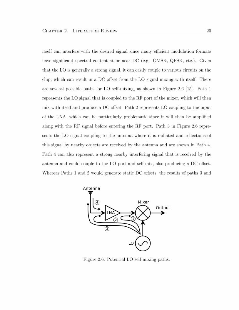
are several possible paths for LO self-mixing, as shown in Figure 2.6 [15]. Path 1
represents the LO signal that is coupled to the RF port of the mixer, which will then
mix with itself and produce a DC offset. Path 2 represents LO coupling to the input
of the LNA, which can be particularly problematic since it will then be amplified
along with the RF signal before entering the RF port. Path 3 in Figure 2.6 repre-
sents the LO signal coupling to the antenna where it is radiated and reflections of
this signal by nearby objects are received by the antenna and are shown in Path 4.
Path 4 can also represent a strong nearby interfering signal that is received by the
antenna and could couple to the LO port and self-mix, also producing a DC offset.
Whereas Paths 1 and 2 would generate static DC offsets, the results of paths 3 and
Figure 2.6: Potential LO self-mixing paths.

Chapter 2. Literature Review 21
4 would be dynamic due to the changing operating environment. Complementary
metal oxide semiconductor (CMOS) technology, in particular, is very susceptible to
LO self-mixing due to the relatively low substrate resistivity that easily allows energy
to couple to other sub-circuits on the chip.
To combat the LO self-mixing problem, several techniques have been suggested
such as the use of a frequency doubler at the output of the LO [16] and the use of a
subharmonic mixer. While fundamental mixers could be used in Figure 2.5, subhar-
monic mixers are very attractive in direct-conversion receivers since they can reduce
LO self-mixing by using an LO frequency that is much lower than the RF. Further-
more, since the frequency of the LO is reduced there can be significant additional
benefits regarding performance and ease of design, as discussed previously.
2.3 Mixer Circuit Review
In this section, a literature review of current state-of-the-art mixer circuits will be
discussed. Fundamental mixers will first be explored, followed by 2× and 4× subhar-
monic mixers.
2.3.1 Fundamental Mixers
2.3.1.1 Diode-Based Mixers
The use of diodes in mixer circuits is extensive. Recent research on diode-based mixers
generally focuses on very high-frequencies where the use of more complex techniques
(e.g. the Gilbert-cell, discussed in the next section) are not possible due to limited
high-frequency transistor performance. Since the work in this dissertation is focused

Chapter 2. Literature Review 22
on FET-based mixers, a literature review of diode-based mixers is beyond the scope
of this thesis.
2.3.1.2 FET-Based Mixers
A plethora of mixer circuits have been realized using field-effect transistors, the most
popular of which is the Gilbert-cell, shown in Figure 2.7 [17]. This mixer can easily be
implemented monolithically using either bipolar transistors or field-effect transistors
and has several advantages such as excellent isolation between its ports due to its
double-balanced structure and can have a reasonably high conversion gain.
The operation of the Gilbert-type mixer is as follows. The differential RF signal is
fed into the gates of the bottom two transistors, M1 and M2, and the differential LO
signal is applied to the upper transistors (M3–M6 ). The upper two pairs of transistors
Figure 2.7: Gilbert-cell mixer.

Chapter 2. Literature Review 23
are cross-coupled and act as current switches, changing the polarity of the currents
flowing through the drain resistors, Rd. The output signal is taken differentially
between v0 and v180. Degeneration resistors can be inserted in the sources of the
bottom (RF) transistors to provide feedback and improve the linearity of the mixer.
Inductors are also commonly used for this purpose, and are preferable from a noise
standpoint, since, ideally, they do not contribute any noise to the system. Of course,
all real inductors have an associated resistance that generates noise, but there can
still be a significant reduction in the overall noise figure for the mixer by using this
technique. The drawback to using degeneration inductors is the additional IC area
that they require. Using on-chip degeneration inductors will use much more area than
resistors, and thus will increase the cost of the chip.
Since this mixer circuit has two stacked transistors, and possibly more depending
on how the current source is implemented, the use of this circuit topology may not be
possible in a low-supply voltage, low-power application. The noise-figure of Gilbert-
cell mixers is obviously technology-dependent, but it can be somewhat high since
there are at least six active devices contributing noise, as well as possibly two or
more resistors. The input reflection coefficient to a Gilbert-cell mixer will be very
high due to the high input impedance presented by the gates of the FETs since they
are predominantly capacitive. To obtain a reasonably good input impedance match,
a matching network is typically required if the mixer is to be used as a discrete
component. This matching network can be implemented using on-chip inductors
and capacitors, or off-chip with packaged inductors/capacitors or transmission line
structures. A matching network on-chip will use a significant area, which will increase
the cost of the circuit. Off-chip matching networks generally require taking the signal

Chapter 2. Literature Review 24
off-chip and then back on which adds noise to the system and the losses may result
in the need for additional amplification.
A recent example of a CMOS Gilbert-cell is presented in [18]. In this work, CMOS
0.13 µm technology was used to realize a wideband 9 GHz to 50 GHz down-convert
mixer. This circuit used the basic Gilbert-cell shown in Figure 2.7 with a couple of
additions. First, on-chip transformers were used to convert the single-ended RF and
LO signals to differential. At the output, source follower buffers were used to drive
the 50 Ω load of either the measurement equipment or the next stage in the receiver.
Finally, a current injection technique was used to increase the gm of the RF transistors,
and improve the overall conversion gain. The mixer achieved a measured conversion
gain of over 5 dB from 9 GHz to 50 GHz and RF–IF isolations of over 40 dB and LO–
RF isolations over 20 dB in this frequency range. The IIP3 of the mixer at 20 GHz
was 1.2 dBm and the noise figure (DSB) was 16.4 dB. The power consumption of the
circuit was 97 mW and the chip was relatively compact at 0.5 × 0.5 mm2.
In [19], another wideband CMOS Gilbert-cell mixer was presented that operated
from 0.3 GHz – 25 GHz. LC ladder matching networks were used to achieve such
a wideband input impedance match. The conversion gain was approximately 10 dB
from 10 GHz to 25 GHz and the return loss was better than −7 dB from 3 GHz
to 25 GHz. The RF–LO and LO–RF isolations were better than 25 dB. The power
consumption of the mixer core was 71 mW. Due to the inductors that were integrated
on-chip, the area of the IC was larger than otherwise would be necessary at 0.8 × 1.0
mm2.
While the most common type of FET mixer is the Gilbert-cell topology (or vari-
ations thereof), there are many other FET circuits that can be used to realize a

Chapter 2. Literature Review 25
fundamental mixer. For example, one popular technique is the resistive FET mixer,
shown in Figure 2.8. Resistive mixers using FETs are passive mixers that use the
nonlinearity of the FET resistance to enable mixing. More specifically, since the LO
is generally a large signal, the non-linear characteristics of the transistor alter the
FET resistance with the LO signal. The FET is generally biased in the resistive, or
triode region of operation, and filters are used for the RF and IF ports. Advantages
of resistive FET mixers include their relative simplicity (compared to Gilbert-cell
mixers, for example) and that they generally do not consume any DC power. How-
ever, they can have significant conversion losses which offsets these advantages. An
example of a FET resistive mixer from the literature is given in [20]. In this work,
90 nm CMOS silicon-on-insulator (SOI) technology was used to realize a 26.5 GHz
to 30 GHz resistive mixer. The circuit in Figure 2.8 was used in [20] with parallel
LC filters for both the RF and IF ports as well as an LO gate inductor for matching.
The conversion loss for this circuit was between 9 dB and 13 dB from 26.5 GHz to
Figure 2.8: Resistive FET mixer.
Chapter 2. Literature Review 26
30 GHz with an LO power of 5 dBm. The IIP3 was 12.7 dB and the single-sideband
noise figure was 11.4 dB. The measured isolations were between 22 dB and 33 dB for
all ports.
2.3.2 Subharmonic Mixers
As discussed previously, direct-conversion receivers convert the received signal directly
to baseband as opposed to first converting to an intermediate frequency. The primary
advantage to using direct-conversion is that there is no image frequency produced,
and, consequently much simpler and inexpensive filtering can be used. To this end,
and to take advantage of the benefits of a lower LO frequency, there have been
many 2× subharmonic mixers (SHMs) demonstrated in the literature. There are
a large number of 2× SHMs based on the APDP configuration discussed earlier in
this chapter, however, there are also many transistor-based 2× SHMs. Since the
circuits proposed in this thesis are FET-based SHMs, the 2× SHM literature review
section will focus on transistor-based subharmonic mixers. In a following section that
examines existing 4× subharmonic mixers there will be a discussion of several APDP
SHMs, since these are the dominant type of 4× subharmonic mixers.
2.3.2.1 2× Subharmonic Mixers
There have been many 2× SHMs proposed (e.g. [21–37]). In most cases (e.g. [22,
23, 31–33, 35, 36]), modifications to the Gilbert-cell mixer (Figure 2.7) were made
in order to generate the double frequency LO component to mix with the RF. One
common modification to the Gilbert-cell to enable subharmonic mixing is by using an
additional level of LO switching transistors and using quadrature LO signals rather

Chapter 2. Literature Review 27
than differential [25, 28, 31, 35]. This circuit, shown in Figure 2.9 with bipolar
transistors, has three-levels of transistors with the 0 and 180 LO signals applied to
the gates of the middle LO-transistor level, and the 90 and 270 LO signals applied
to the gates of the top LO-transistors. This configuration generates the doubled LO
frequency signal, 2fLO, that mixes with the differential RF signal that is applied
to the gates of the bottom transistors. Since this technique requires three levels of
transistors, it generally requires a higher DC supply voltage than the basic Gilbert-
cell and its use may not be possible in low-voltage applications. The topology shown
Figure 2.9: Basic 2× subharmonic mixer circuit used in [25, 28, 31, 35].

Chapter 2. Literature Review 28
in Figure 2.9 was introduced by [35], where it was implemented using a Si/SiGe HBT
technology and using passive on-chip RC phase shifters to generate quadrature LO
signals. This circuit was designed for direct-conversion applications with an RF signal
from 1 GHz to 2 GHz and an LO frequency from 500 MHz to 1 GHz. With a DC
supply voltage of 2.5 V, the measured conversion gain was 13.5 dB with an LO power
of 10 dBm, a double sideband (DSB) noise figure of 10.4 dB, an IIP2 of 29.7 dBm,
and an IIP3 of −3.5 dBm.
The circuit shown in Figure 2.9 was also used in [31] with a SiGe BiCMOS process.
Polyphase filters were used to generate the required quadrature LO signals in this
work and the circuits was designed for RF signals from 5 GHz to 6 GHz and an IF of
50 MHz. The voltage conversion gain of the mixer was measured to be 6 dB, with an
IIP2 of 29 dBm. The 2LO–RF isolation was measured to be greater than 55 dB and
the LO–RF isolation was greater than 50 dB. The power consumption for the mixer
was 16.5 mW and the chip area was 2.3 mm × 1.8 mm.
A circuit similar to the one in Figure 2.9 was also used in [28], however, in this
work CMOS 0.13 µm technology was used and the circuit was adjusted for passive
operation. The circuit was designed for 24 GHz direct-conversion applications and
used an RF preamp as well as LO and IF buffers. The quadrature LO signals were
generated using an off-chip 90 hybrid along with on chip active baluns. The measured
overall conversion gain of the circuit was 3.2 dB and the DSB noise figure was 10 dB.
The 1-dB compression point was −12.7 dBm and the power consumption including
the RF preamp and buffers was 13.6 mW. The measured 2LO–RF isolation was 57 dB
and the size of the fabricated chip was 0.9 mm × 0.65 mm.

Chapter 2. Literature Review 29
Yet another implementation of the basic subharmonic mixer circuit shown in Fig-
ure 2.9 is presented in [25]. In this work, an RC–CR phase shifter network is used
to generate the required quadrature LO signals and CMOS 0.18 µm technology was
used for RF input signals in the 5 GHz band. The measured maximum conversion
gain of this circuit was 9.5 dB and the LO–RF isolation was 48 dB. The IIP3 was
−7.5 dBm, the 1-dB compression point was −20 dBm, and the power consumption
was 17.5 mW.
A different modification to the Gilbert-cell to enable 2× subharmonic mixing is
demonstrated in [36] using a 0.35 µm BiCMOS technology. This circuit, which is
shown in Figure 2.10, uses only two levels of transistors similar to the traditional
Gilbert-cell, however, it exchanges the position of the LO and RF transistor (i.e. the
LO transistors are on the bottom and the RF transistors are on the top). Similar to
the circuit in Figure 2.9, quadrature LO signals are also required for this topology.
In [36], the quadrature signals were generated on-chip from a differential LO input
using RC–CR networks. The circuit in [36] was designed for an RF signal at 1.9 GHz
and an LO signal at 900 MHz (a 100 MHz IF). The measured conversion gain for
this circuit was 7.5 dB and the single-sideband (SSB) noise figure was 10 dB. The
input 1-dB compression point was −8 dBm and the IIP3 was −3 dBm. The power
consumption was 24 mW.
A comparison between the three most common transistor-based 2× subharmonic
mixers circuits is presented in [33]: (1) the circuit in Figure 2.9 (three-level), (2)
LO transistors on the bottom (Figure 2.10), and (3) LO transistors on the top (not
shown, but used in [23]). It was found through this comparison that the circuit
topology in Figure 2.9 can operate with the lowest LO power levels, but requires a

Chapter 2. Literature Review 30
Figure 2.10: Subharmonic mixer circuit proposed in [36].
higher DC voltage supply compared to the other two topologies. Furthermore, the
circuit in Figure 2.9 has the lowest maximum operating frequency out of the three
topologies. The bottom-LO SHM shown in Figure 2.10 has advantages in terms of
power consumption, linearity, RF–IF isolation, and noise figure. The third topology
discussed (LO transistors on top, [23]) can achieve a higher conversion gain and higher
2LO–RF isolation.
Clearly, from the preceeding discussion of 2× subharmonic mixers, the requirement
of quadrature LO signals is very common (e.g. [22–25, 28, 32, 36]). Furthermore, in
[29–31], octet-phase signals of the LO were used with subharmonic mixers.
There are several circuits that have been used to realize 2× subharmonic mixers
using FETs that are not based on the Gilbert-cell. For example, in [37], the RF
Chapter 2. Literature Review 31
signal was applied to the gate of a FET while the LO signal was applied to the bulk
connection of the FET (using CMOS 0.18 µm technology). This technique of injecting
the LO signal into the bulk of the transistor has the effect of modulating the threshold
voltage and exploiting the non-linearity that results to realize a subharmonic mixer.
The measured conversion gain in [37] was 10.5 dB with an RF frequency of 2.1 GHz
and LO frequency of 1.025 GHz. The input 1-dB compression point was −12 dBm
and the IIP3 was −3.5 dBm. The measured noise figure (DSB) was 17.7 dB and the
power consumption was 2.5 mW.
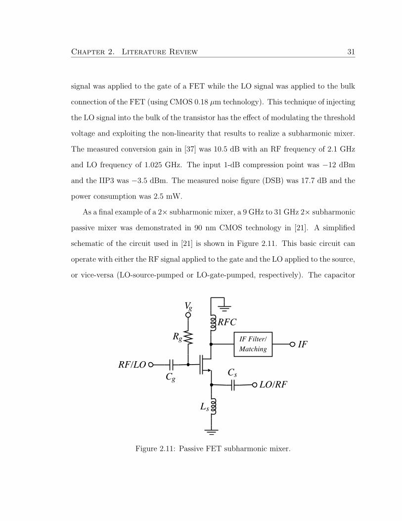
As a final example of a 2× subharmonic mixer, a 9 GHz to 31 GHz 2× subharmonic
passive mixer was demonstrated in 90 nm CMOS technology in [21]. A simplified
schematic of the circuit used in [21] is shown in Figure 2.11. This basic circuit can
operate with either the RF signal applied to the gate and the LO applied to the source,
or vice-versa (LO-source-pumped or LO-gate-pumped, respectively). The capacitor
Figure 2.11: Passive FET subharmonic mixer.

Chapter 2. Literature Review 32
Cg is used primarily as a DC-block and Ls and Cs are used as a high-pass filter and for
input matching. The FET’s gate bias is provided by Vg through a large resistor, Rg.
Since it is a passive mixer, there is no DC current through the transistor (both the
drain and source are DC-ground). The implementation of the circuit in Figure 2.11
in [21] used a π-network composed of two capacitors and one inductor to implement
a low-pass filter at the IF output. This circuit is unique in that it can operate with
either a 12fLO or 1
3fLO (i.e. either a 2× or 3× SHM). The conversion loss for the 2×
SHM-mode was between 8 dB to 11 dB over the RF frequency range and it was 12 dB
to 15 dB for the 3× SHM-mode over the RF frequency range. The IIP3 was 3 dBm
for the 12-LO source pumped mode and 7 dBm for the 1
3-LO source-pumped mode.
The minimum 2LO–RF isolation for the 12-LO source-pumped mode was 27 dB over
the band of operation and the minimum 3LO–RF isolation was 45 dB for the 13-LO
source pumped mode. The dimensions of the fabricated chip were 0.9 mm × 1.0 mm
and given its passive operation there was no DC power consumption used by this
SHM.
2.3.2.2 4× Subharmonic Mixers
There have been several 4× SHMs previously demonstrated [38–43]. The vast major-
ity of these circuits used diodes to perform the mixing, which eliminates the possibility
of achieving conversion gain. As discussed previously, it is possible to use an anti-
parallel diode pair for subharmonic mixing, and this diode configuration conveniently
cancels some of the undesired mixing products. In fact, nearly all 4× SHM circuits
use an APDP and filters in configurations such as the one shown in Figure 2.12.
For example, in [41], an APDP was used for a direct-upconverter using the

Chapter 2. Literature Review 33
Figure 2.12: Subharmonic mixer using an anti-parallel diode-pair.
basic circuit shown in Figure 2.12. The RF and IF filters were implemented by
an RF/baseband duplexer that used coupled-line filters combined with a stepped
impedance low-pass filter and rejection stubs. A transmission line matching network
was used for the LO signal to minimize the LO input reflection coefficient. In this
work, a baseband input signal was used along with a ∼10 GHz LO signal to produce
a ∼40 GHz RF output signal. The measured isolation between the RF and IF (base-
band in this case) ports was greater than 30 dB. The conversion loss of this hybrid
microwave circuit was quite high (21 dB to 15 dB, as the LO power is increased from
6 dBm to 11 dBm).
An MMIC implementation of the APDP circuit shown in Figure 2.12 was presented
in [39]. In this work, a 94 GHz quadruple subharmonic mixer (4× SHM) was designed
and measured using GaAs MESFET technology. A coupled-line bandpass filter was
used for the RF port and stub filters were used at the IF and LO ports. The 94 GHz
RF input signal was mixed with a ∼23.5 GHz LO input signal to down-convert the
RF to a 100 kHz IF. The maximum conversion gain for this design was measured

Chapter 2. Literature Review 34
to be −11.4 dB at an LO input power of 10 dBm and the input 1-dB compression
point of this SHM was approximately −6 dBm The fabricated chip dimensions were
0.9 mm × 1.4 mm.
In [40], a 4× SHM was presented again using APDP in a hybrid implementation
with two packaged diodes and a 10 mil duroid substrate. The RF signal used in this
work was in the upper Ka-band (38.5 GHz to 40 GHz) and the LO frequency was in
X-band, which produced a IF output centered at 2.5 GHz. Matching and filtering for
all three ports was accomplished primarily with transmission line stub filters. The
minimum conversion loss of this circuit was measured to be 9 dB and the return loss
for the RF, IF, and LO ports was approximately −20 dB, −20 dB, and −15 dB,
respectively.
In the GaAs-based MMIC APDP-based 4× subharmonic mixer presented in [38]
a number of anti-parallel diodes were used in addition to transmission line stub filters
in order to extract the signal at (ωRF − 4ωLO). More specifically, this design replaced
the single APDP shown in Figure 2.12 with a triple diode implementation (six diodes
in total with three in each direction). The purpose of the triple APDP was to reduce
the diode series resistance in an attempt to decrease the conversion loss of the mixer.
The circuit operates with an LO input frequency range from 12 GHz to 16 GHz and
RF input frequency range from 50 GHz to 65 GHz. The minimum conversion loss
for the circuit is 11 dB with a 7 dBm LO input signal. The LO–IF isolation was
measured to be as low as 17 dB and the LO–RF isolation was measured to be as
low as 33 dB in the intended frequencies of operation (other isolation measurements,
such as 4LO–RF were not given). Linearity measurements were not reported for this
work.

Chapter 2. Literature Review 35
As a final example of a 4× SHM based on the APDP circuit shown in Figure 2.12,
a V-band MMIC was presented in [42]. This work used GaAs PHEMT technology
along with CPW transmission lines. Stub filters were used for the RF and LO signals,
while lumped element inductors and capacitors were used for IF matching and low-
pass filtering. In addition to the APDP, this design also used FETs for amplification,
which enables the possibility of obtaining conversion gain from the overall circuit
(the APDP that does the actual mixing of course still has a conversion loss). The LO
frequency was 14.5 GHz and the RF signal was 60.4 GHz, producing an IF output at
2.4 GHz. Th maximum measured conversion gain was 0.8 dB for an LO input power
of 12 dBm. The LO–RF and LO–IF isolations were both higher than 40 dB. The
dimensions of the fabricated MMIC were 1.9 mm × 2.6 mm.
One of the very few instances where a 4× subharmonic mixer has been demon-
strated not using diodes is presented in [43]. In this work, GaAs MESFETs were used
in a cascode configuration along with several stubs for RF and LO port filtering. The
FETs were used to generate and enhance the fourth harmonic of the LO input signal
and then mix it with the input RF signal. Lumped inductors and capacitors were
used at the IF output for both matching and low-pass filtering. The RF range for this
circuit was from 59.4 GHz to 60.9 GHz with an LO input frequency of 14.5 GHz. The
measured conversion gain was 2.5 dB to 3.4 dB for an LO input power of 13 dBm. Iso-
lation measurements showed an LO–RF isolation of 46.2 dB and an LO–IF isolation
of 53.6 dB. The fabricated chip dimensions were 1.9 mm × 1.8 mm.
Generally, and as would be expected, 4× SHMs have more loss than 2× SHMs,
which in turn generally have more conversion loss that fundamental mixers. In most
cases, 4× subharmonic mixers do not exhibit a conversion gain.

Chapter 2. Literature Review 36
2.4 Oscillators Circuit Review
Oscillators are fundamental components in wireless communications systems that can
be used for several applications. Communication systems that use phase shift keying
modulation frequently require a pair of LO signals that are in quadrature, or 90 out-
of-phase. Furthermore, quadrature signals are commonly required in direct-conversion
receivers or low-IF systems as well as in digital radio communication systems such as
GSM and DECT [44]. Every mixer, whether fundamental, or subharmonic, requires
a local oscillator signal, and as such, a literature review of CMOS oscillator circuits
will be presented in this section.
2.4.1 Resonators for CMOS Microwave Oscillators
A microwave resonator is the component in a microwave oscillator that determines
the frequency of oscillation. There are many ways to implement a resonator. The
decision as to which type to use can depend on many factors, such as operational
frequency, required performance, cost, and required area. A resonator can be as
straight-forward as a series or parallel LC network, and in fact, almost all CMOS
oscillators use simple LC resonators. Regardless of what type of resonator is used,
most resonators can be modeled as a parallel or series RLC circuit around resonance.
The resonant frequency for parallel and series RLC resonant circuits is given by:
ω0 =1√LC
. (2.17)
The quality factor, or Q-factor, is a characterization of the loss of a resonant structure
(higher Q implies lower loss). It is defined as
Q = ωAverage energy stored
Energy loss per second(2.18)

Chapter 2. Literature Review 37
and for a series RLC circuit, it is:
Q =1
ω0RC. (2.19)
For a parallel RLC circuit, the Q-factor is given by:
Q = ω0RC. (2.20)
LC resonators are the easiest to implement on-chip at relatively low microwave fre-
quencies, and are the type used for most CMOS oscillators. However, the Q-factor
of the resonant circuit can be quite low due primarily to the low quality factor of the
inductor, which can lead to poor phase noise performance. In fact, the phase noise
of an oscillator is proportional to 1/Q2. Therefore, by improving the Q-factor of the
inductor (which is usually the limiting element in the Q-factor of an LC resonator)
the performance of the oscillator can be vastly improved.
Spiral inductors in standard CMOS technology are often modeled as shown in
Figure 2.13 [45]. In this model, Ls is the low-frequency inductance, Rs is the series
resistance of the coil, Cs is the capacitance between the different windings of the
inductor, C1 and C2 are the capacitances in the oxide layer between the coil and the
substrate, Cp1 and Cp2 are the capacitances between the coil and the ground through
the silicon substrate, and Rp1 and Rp2 are the eddy current losses in the substrate.
This model has proven to be an accurate representation of CMOS inductors and is
used extensively. While minor performance improvements can be obtained in CMOS
inductors by using patterned ground shields [46], they are generally limited to about
Q < 20 by the intrinsic properties of the CMOS process (and often have a Q-factor
of about 5 in CMOS 0.18 µm technology). It is therefore very difficult to design an
oscillator in CMOS technology that has very low phase noise.

Chapter 2. Literature Review 38
CS
L S RS
Cp2
C2
Cp1
C1
Rp1 Rp2
Figure 2.13: Common model used for CMOS inductors.
2.4.2 Common Oscillator Topologies
There are many different oscillator topologies that can be used to implement mi-
crowave oscillators in CMOS technology. This section will focus on the state-of-the-
art for two of the most common oscillator topologies in CMOS: the Colpitts oscillator
and the cross-coupled FET oscillator. Lastly, techniques for generating quadrature
output signals are discussed.
2.4.2.1 Colpitts Oscillator
A very common oscillator circuit that can easily be implemented monolithically is the
Colpitts oscillator, one configuration of which is shown in Figure 2.14. The detailed
analysis of this circuit is covered in many standard microelectronics texts (e.g. [47])
and will not be repeated here. Essentially, the circuit oscillates by providing positive
feedback from a capacitive voltage divider to an amplifier. The oscillation frequency

Chapter 2. Literature Review 39
Figure 2.14: Colpitts oscillator circuit.
is given by:
ω0 =1√LCeq
(2.21)
where
Ceq =C1C2
C1 + C2
. (2.22)
This circuit is more applicable to CMOS integration compared to other variants of
this oscillator topology. For example, the Hartley oscillator uses a tapped inductor
for feedback rather than a tapped capacitor, and is therefore much less attractive
for CMOS implementations. Of course, the performance of this oscillator will be
primarily determined by the quality of the resonator, and thus the quality of the
inductors and capacitors used.
An example of a CMOS Colpitts oscillator from the literature is demonstrated

Chapter 2. Literature Review 40
in [48]. In this work, a 5 GHz Colpitts oscillator using 0.18 µm technology was
presented. A differential form of the standard Colpitts oscillator was used along with
varactors in the place of static capacitors. In the differential version of the Colpitts
oscillator, two single-ended Colpitts oscillators (Figure 2.14) were coupled to ensure
odd-mode oscillation (and suppression of even-mode oscillation). The tuning range
of the circuit was from 4.61 GHz to 5.0 GHz and the output power was 4 dBm. The
phase noise was measured to be −120.42 dBc/Hz at a 1 MHz offset and the DC power
consumption of the oscillator core was 3 mW.
2.4.2.2 Cross-Coupled MOSFETs
The cross-coupled FET oscillator is the most common microwave oscillator topology
used in CMOS technology. An LC oscillator can be modeled with the capacitor
and inductor in parallel with a resistor to model the losses in the tank as well as a
negative resistance that models the active device. One way of generating the negative
resistance to compensate for the losses in the LC tank is to use a cross-coupled
differential pair as shown in Figure 2.15. The resistance, Rin, looking into the cross-
Figure 2.15: Negative resistance generated from cross-coupled FETs.

Chapter 2. Literature Review 41
coupled pair is given by:
Rin = − 2
gm
, (2.23)
where gm is the transconductance of each of the FETs in the cross-coupled pair.
Therefore, with an appropriate device size and biasing, the value of negative resistance
required to counteract the losses in the tank can be realized. A commonly used LC
oscillator circuit using the cross-coupled differential pair is shown in Figure 2.16. In
this implementation a relatively low supply voltage is possible since there are only
two levels of transistors, but it requires two inductors, which can consume significant
chip area.
The oscillator topology shown in Figure 2.16 was used in [49]. In this work,
CMOS 0.13 µm technology was used to design a 60 GHz VCO with a 6 GHz tuning
range. The capacitor shown in Figure 2.16 was replaced with a varactor to enable
the frequency tuning. The signal output power was approximately −10 dBm and the
Figure 2.16: Cross-coupled FET oscillator.

Chapter 2. Literature Review 42
phase noise at a 1 MHz offset was −90.7 dBc/Hz.
A slight modification to this topology is shown in Figure 2.17. It has been shown
[50] that by including the cross-coupled PMOS transistors at the top of the circuit the
phase noise can be reduced considerably. Furthermore, only one inductor is required,
which is an advantage over the previous circuit. However, since there are now three
levels of transistors, implementations with a very low power supply such as in [51]
would not be possible with this configuration. The oscillation frequency for this
circuit can be found from the formula for the resonant frequency of an LC tank:
f0 =1
2π√LCtot
, (2.24)
Figure 2.17: Complementary cross-coupled FET oscillator.

Chapter 2. Literature Review 43
where L is the value of the on-chip spiral inductor and Ctot is the total capacitance
between the drains of the two cross-coupled transistors (including any parasitic ca-
pacitance). Of course, by using a varactor instead of the static capacitor in the tank,
a voltage controlled oscillator can be realized.
A circuit using the cross-coupled topology shown in Figure 2.17 was described in
[52]. Standard CMOS 0.18 µm technology was used in this design to realize a VCO
that operates from 9.3 GHz to 10.4 GHz. The phase noise performance was −89 dBc
at a 100 kHz offset and the DC power consumption of the VCO core was 5.8 mW.
The spiral inductor (0.5 nH) had a Q-factor of 10 while the varactor had a Q-factor
of 38.
2.4.2.3 Quadrature Oscillators
The oscillator circuits discussed above produce either a single-ended or a differen-
tial output signal. There are several techniques that can be employed to generate
quadrature signals. One straight-forward method is to use an RC–CR phase shift
network with a standard oscillator to create a 90 phase shift [53]. Since the phase
shift is completely dependent on the values of the resistors and capacitors, any devi-
ation in the fabricated values of these components will directly lead to a error in the
accuracy of the quadrature signals. Resistors, in particular, have large tolerances in
most CMOS processes, and therefore this method can lead to poor accuracy in the
quadrature signals that are generated.
Another approach to generate quadrature signals is to use a digital divide-by-
two frequency divider that follows an oscillator running at twice the fundamental
frequency [54]. The use of this technique at high frequencies is inherently limited

Chapter 2. Literature Review 44
since an oscillator operating at double the desired frequency is required.
A third common technique is to force two VCOs to run in quadrature by using
coupling transistors working at the fundamental frequency [55]. This technique suf-
fers from a trade-off between quadrature accuracy and phase noise due to the effects
of the coupling circuit on the oscillation frequency. To avoid this problem, a quadra-
ture oscillator can be realized using superharmonic coupling. As illustrated in Figure
2.18a, by employing differential coupling at the common-mode nodes where the sec-
ond harmonic is predominant, quadrature signals are generated at the fundamental
frequency. To implement the coupling of the second harmonic with a 180 phase shift,
an inverting on-chip transformer has been used [56–58] (Figure 2.18b).
CouplingCircuit
IndependentOscillators at f0
2 00 180
o o
(a)
(c)(b)
Common-ModeNodes
K
To CM NodeOsc1 Osc2
To CM NodeOsc1 Osc2
Osc1 Osc2
0 ato
f0 90 ato
f0
f2 0f2 0f
Figure 2.18: Quadrature oscillator superharmonic coupling techniques.

Chapter 2. Literature Review 45
In [57], passive superharmonic coupling was used with an on-chip transformer in
0.35 µm technology to enforce a quadrature relationship between two cross-coupled
oscillators (similar to Figure 2.17). This VCO was tunable from 4.57 GHz to 5.21 GHz
and achieved a phase noise of −138 dBc/Hz at a 1 MHz offset. The output signal
power was −9 dBm, the DC power consumption of the oscillator core was 5.1 mW,
and the dimensions of the chip were 1250 µm × 1250 µm. The disadvantage of
the passive superharmonic coupling technique in general is that on-chip transformers
consume a significant area on-chip and have a limited Q-factor, particularly in CMOS
technology.
A method of replacing the inverting transformer with a cross-coupled differential
pair was proposed in [59] (Figure 2.18c), which can significantly reduce the required
chip area. In [59], a quadrature voltage controlled oscillator was designed at 6 GHz
in SiGe technology using the coupling circuit shown in 2.18c along with two of the
oscillator circuits shown in Figure 2.16. The measured output power was −5.3 dBm
and a 24% tuning range was obtained. The phase noise at a 1 MHz offset was
measured to be −105.8 dBc/Hz.
2.5 Frequency Multiplier Circuit Review
Frequency multiplier circuits are used in a wide range of applications in communi-
cation systems. They are fundamental components that are often used to generate
a high-quality reference signal, as well as in frequency synthesizers. Using frequency
multiplication, oscillators can be designed at lower frequencies and then converted
to higher ones, which can simplify the design of the oscillator, possibly improve the
phase noise of the resulting signal, and reduce power consumption. The phase noise

Chapter 2. Literature Review 46
of a signal going through a frequency multiplier is degraded by 20log(n), where n is
the order of multiplication. However, the resulting phase noise is often an improve-
ment over the performance of an oscillator that is designed to operate directly at the
higher frequency. Furthermore, it is also possible that the incorporation of frequency
multipliers can reduce the number of voltage controlled oscillators (VCOs) required in
multi-band transceivers. Frequency doublers are most often used because they gener-
ally offer greater conversion gain (or lower conversion loss) compared to higher-order
multipliers. This section will present a literature review of several common frequency
multiplier circuits.
2.5.1 Common Frequency Multiplier Topologies
2.5.1.1 Single-FET Frequency Multipliers
Many CMOS frequency multiplier circuits have been demonstrated using various
methods. A common technique is to use the nonlinearities of a transistor with a large
input signal such as in [60]. A simplified schematic of this type of frequency multiplier
circuit is shown in Figure 2.19 as a frequency doubler. With this method, the out-
put has many harmonic spectral components that are generated from the non-linear
I–V characteristic of the FET, among which is the desired output frequency signal.
As shown in Figure 2.19, input matching at the fundamental frequency is generally
used, along with filtering and matching for the desired frequency component at the
output. In [60], the basic circuit shown in Figure 2.19 was used to realize a frequency
doubler using CMOS 90 nm silicon-on-insulator (SOI) technology. Lumped induc-
tors and capacitors were used for input matching and for output matching/filtering.
The DC voltages were applied through the matching/filtering circuits, which elim-

Chapter 2. Literature Review 47
Figure 2.19: Simplified frequency doubler using FET non-linearities.
inated the need for RF chokes. This circuit operated with input signal frequencies
between 13.25 GHz and 14.25 GHz to produce an output signal between 26.5 GHz
and 28.5 GHz. A maximum conversion gain of 1.5 dB was measured and the input
return losses for both ports were approximately 10 dB. The suppression of the fun-
damental was less than 10 dB at the output, and only 5 dB at the input power level
where the conversion gain of 1.5 dB was obtained. The circuit is very compact at
0.37 mm × 0.27 mm and the DC power consumption was 10 mW.
2.5.1.2 Common-Mode Node Frequency Multipliers
Another frequency multiplier technique is to use the common-mode output nodes of
an oscillator. Shown in Figure 2.20 is a simplified circuit demonstrating an injected
fundamental signal, fin, which forces the cross-coupled oscillator to lock to this fre-
quency. The doubled frequency, 2fin can then be obtained at the common-mode
node as shown in the figure. This technique was used in [61] where a regenerative

Chapter 2. Literature Review 48
Figure 2.20: Simplified circuit of an injection-locked frequency doubler.
frequency doubler was designed using a two-stage cross-coupled ring topology in a
standard CMOS 0.35 µm process. In this work, quadrature clock phases were used as
input and a differential output was taken at two common-mode nodes. The maximum
operating frequency for this design was 4.0 GHz with a bandwidth of 2.4 GHz. The
conversion loss was measured to be 2 dB to 4 dB and the phase noise degradation was
close to 6 dB (the theoretical minimum for a frequency doubler is 20log(2) = 6.02 dB).
The core area of the doubler circuit is extremely small in this work (79 µm × 74 µm)
since no passive components were required (although they likely would be required
for biasing and an output buffer, which significantly increases the chip size). The
power consumption for this circuit was low at 3.7 mW.

Chapter 2. Literature Review 49
2.5.1.3 Push-Push Frequency Multipliers
Push-push circuits have also been used for frequency doubling. For example, in [62]
a low-power fully differential frequency doubler is presented (shown in Figure 2.21).
Essentially, this technique uses switches to connect the output to the 0 input signal in
one half of the input signal period, and the 180 input signal during the other half of
the input signal period. The resulting waveform at the output resembles an absolute
value waveform, which clearly contains a strong second harmonic component. In [62],
CMOS 0.25 µm technology was used with a 450 MHz input signal (900 MHz output).
The measured conversion loss was 4 dB and the circuit showed strong suppression
of the fundamental (over 50 dB in simulations). Given this circuit’s complementary
structure, it consumes very little DC power. The exact amount of DC power consumed
Figure 2.21: Push-push frequency doubler circuit.

Chapter 2. Literature Review 50
by this doubler was not reported (the doubler was combined with a mixer and only
the overall DC power consumption was given).
2.5.1.4 Odd-Order Frequency Multipliers
In order to realize odd-order frequency multipliers, such as a frequency tripler, custom-
built devices such as heterostructure and quantum barrier varactor diodes [63–65]
with strongly non-linear I–V curves are regularly used. To circumvent the use of
non-standard semiconductor devices, triplers can be realized by overdriving a transis-
tor with the sinusoidal input signal to generate a clipped waveform rich in odd-order
harmonics [66–70]. This method, however, usually requires strong filtering at the out-
put to remove the fundamental and other unwanted frequencies. Often, the filtering
has to be accomplished off-chip to improve signal rejection. Balanced frequency tripler
circuits based on extracting the third harmonic generated by FET non-linearities are
presented in [71, 72] with on-chip filtering and cancellation of unwanted harmonics,
but the required chip area can be very large (e.g. 5.0 mm2 in [71] and 2.32 mm2 in
[72]).
Injection-locking can also be used to implement a frequency tripler [73, 74], al-
though, the resonator used in the oscillator can consume large chip area and can limit
the bandwidth of the circuit. Recent advances in integrated circuit tripler design [75]
have used waveform shaping techniques in order to generate the triple frequency and
to relax the output filter requirements. In [75], rather than clip a sinusoidal signal
and then extract the third-harmonic, “deep-cuts” were made at the peaks of the
sinusoidal input, which results in an enhanced third-harmonic output. In order to
generate these cuts in the waveform, an inverter was used along with a non-linear

Chapter 2. Literature Review 51
combiner circuit. Since this technique generates a strong third harmonic and natu-
rally suppresses the fundamental, a simple low-Q high-pass filter can be used on-chip
to further attenuate the fundamental to a level that would be acceptable for most ap-
plications. CMOS 0.18 µm technology was used in [75] and the circuit was designed
for an input frequency range from 1.7 GHz to 2.25 GHz (output frequencies from
5.1 GHz to 6.75 GHz). The minimum measured conversion loss using this technique
was 5.6 dB and the fundamental suppression at the output was more than 11 dB. The
circuit was very compact at 420 µm × 320 µm including pads, and the DC power
consumption was 27 mW.
2.5.1.5 Digital Frequency Multipliers
There are many digital frequency multiplier techniques that have been demonstrated.
For example, an all-digital clock multiplier is proposed in [76] for low-frequency clock
references that can achieve 2×, 3×, or 4× frequency multiplications. In general,
digital frequency multiplier techniques have lower operational frequency limits than
their analog counterparts and often have higher power consumptions. Given the
microwave focus of this thesis, digital frequency multiplier techniques will not be
discussed in detail.
2.6 Frequency Divider Circuit Review
Frequency dividers can be used in many applications, but are most often used in
the feedback path of phase-locked loops (PLLs) in order to achieve frequency mul-
tiplication. In the vast majority of frequency dividers presented in the literature an
even-order division ratio is used. In fact, most frequency dividers divide the frequency

Chapter 2. Literature Review 52
of an input signal by a factor of two or four and there are very few odd-order fre-
quency dividers that have been demonstrated. In this section a literature review will
be presented of common circuit techniques that can be used to realize a frequency
divider.
2.6.1 Common Frequency Divider Topologies
2.6.1.1 Digital Frequency Dividers
Many frequency dividers used in PLLs and in other applications use digital flip-flop
based dividers. These digital frequency dividers have several advantages, such as
wide-band operation and the potential for high division ratios (e.g. [77]). However,
digital dividers often have very large power consumptions and in fact can consume
a very large percentage of the overall DC power used by frequency synthesizers used
in modern wireless systems [78]. Furthermore, the maximum operational frequency
of digital frequency dividers is generally lower than in narrow-band analog frequency
dividers. Given the narrow-band nature of most wireless signals it is possible to use
analog techniques to achieve higher operational frequencies and also reduced power
consumption. Given these advantages of analog dividers, as well as this thesis’ focus
on analog circuits, digital frequency divider techniques will not be discussed in detail.
2.6.1.2 Regenerative Frequency Dividers
A well-known analog frequency divider topology is the regenerative topology, shown
in Figure 2.22 and first introduced by Miller in 1939 [79]. As shown in the figure, in
its simplest form the regenerative divider consists of a mixer and a low-pass filter. If
the input signal to this circuit has a frequency fin then there are two steady-state

Chapter 2. Literature Review 53
Figure 2.22: Simplified circuit of a regenerative frequency divider.
outputs of the mixer, 12fin and 3
2fin. The low-pass filter attenuates the 3
2fin signal,
thus leaving the 12fin for the output and for feedback. In practical implementations
of the regenerative frequency divider technique an amplifier may also be required
after the filter in order to achieve the required gain around the feedback loop that
will enable the circuit to operate. Practical implementations of this technique are
presented in [80] and [81]. In [80], a 40 GHz frequency divider was designed in CMOS
0.18 µm technology that consisted of two Miller divider stages that divided the input
40 GHz signal to 10 GHz at the output. The mixers used in this work were modified
Gilbert-cells that used inductive loads to achieve higher frequency operation as well
as the filtering required for the regenerative topology. This circuit obtained an input
bandwidth of approximately 2.5 GHz and required a minimum input power of 3 dBm
to operate. The conversion loss for this circuit was quite high at around 19 dB and
the power consumption was 77.5 mW.
The regenerative frequency dividers demonstrated in [81] used GaAs technology
to realize both a 28 GHz and a 14 GHz version of their frequency divider design. In
this work, a single-FET mixer was used along with a tuned amplifier and coupler for

Chapter 2. Literature Review 54
the feedback path consisting of lumped inductors and capacitors. Conversion gain
was obtained for both the 28 GHz and 14 GHz versions of this frequency divider
design with DC power consumptions of approximately 100 mW. Both versions also
reject the fundamental signal by at least 15 dB and have bandwidths of 11% and
5.7% for the 14 GHz and 28 GHz versions, respectively.
2.6.1.3 Injection-Locked Frequency Dividers
As discussed in the previous sections, it is possible to lock an oscillator to an injected
signal. In the frequency multiplier implementation described previously, an input
signal was injected to lock the fundamental oscillation frequency with the external
signal’s frequency and then the doubled frequency component was taken as the output
at a common-mode node (see Figure 2.20). A similar technique can be used to realize
a frequency divider [82–85]. For example, a simplified cross-coupled injection-locked
frequency divider is shown in Figure 2.23. In this circuit, the input signal is injected
to a common-mode node, which locks the frequency of the oscillator second harmonic
to this external signal frequency. The result of this configuration is an output signal
frequency that has been divided by a factor of two relative to the injected signal.
An injection-locked frequency divider very similar to the circuit shown in Figure
2.23 is presented in [82] using CMOS technology and a division ratio of two. In
this work, an input signal at around 3 GHz was injected to the gate of the bottom
transistor shown in Figure 2.23, which locked the fundamental oscillator output to half
the frequency of the input signal. With no input signal, the free-running oscillation
frequency was 1.6 GHz, and with an input signal a locking range of 370 MHz was
measured with a DC power consumption of only 1.2 mW.

Chapter 2. Literature Review 55
Figure 2.23: Simplified circuit of an injection-locked frequency divider.
Another harmonic injection-locked frequency divider was demonstrated in [83]
using 0.18 µm SiGe BiCMOS technology at 60 GHz (bipolar transistors were used
in this work exclusively). This circuit divided the input signal frequency by a factor
of four by mixing it with the third-harmonic of the output signal (generated by an
inverter). This frequency divider operated with input frequencies from 59.77 GHz
to 60.12 GHz, which is a locking bandwidth of 350 MHz. The circuit required an
input power of at least 0 dBm and had an output power of −16.6 ± 0.5 dBm over
the locking range. The power consumption of this circuit was 50.4 mW and the chip
dimensions were 0.8 mm × 0.7 mm.
One of the relatively few odd-order frequency dividers is presented in [84]. This
injection-locked divide-by-three circuit uses a modified version of the circuit shown
in Figure 2.23. Specifically, a differential input was applied to the gates of two

Chapter 2. Literature Review 56
transistors, as opposed to the single-ended input applied to the gate of the single
transistor at the bottom of Figure 2.23 and the sources of the cross-coupled transistors
are no longer connected. This circuit was implemented in CMOS 0.18 µm technology
at an input frequency of 18 GHz. As with most injection-locked frequency dividers,
the locking range increases as the input power increases. In this circuit, the locking
range was 300 MHz for an input power of −14 dBm and 1 GHz for an input power of
0 dBm. The suppression of the undesired harmonics at the output were −23 dB for
the second harmonic and −21 dB for the third harmonic relative to the fundamental
output power level. The power consumption for the core of this divider circuit was
4.6 mW (45 mW including buffers) and the chip dimensions were 0.9 mm × 0.9 mm.

Chapter 3
A 2x Subharmonic Mixer in CMOS
3.1 Introduction
In this chapter, the design and measurement of a CMOS 2× subharmonic mixer that
uses active baluns at the input and at the output is presented. This circuit, which
was published in [8], could be used in either a superheterodyne system to reduce the
required LO frequency by half, or in a direct-conversion receiver in order to reduce
LO self-mixing. As discussed in Chapter 2, the vast majority of subharmonic mixers
are realized with diodes, and as such cannot achieve a conversion gain. The goal
of this work was to realize a subharmonic mixer in a standard CMOS technology
that can achieve a conversion gain and is compatible with a system that uses single-
ended signals. This work is one of the first subharmonic mixers demonstrated with
measurement results in a standard CMOS fabrication technology, and is the first using
the proposed topology. This circuit provides the foundation for a more advanced
higher-order and higher-frequency SHM explored in Chapter 4.
57

Chapter 3. A 2x Subharmonic Mixer in CMOS 58
3.2 Concept of the 2x Subharmonic Mixer
In order to realize an active subharmonic mixer, modifications to the Gilbert-cell have
been shown in [36] and [86] to use four LO signals with relative phase shifts of 0,
90, 180, and 270 to effectively provide switching at twice the rate of the traditional
Gilbert-cell. A block diagram of the subharmonic mixer using this technique is shown
in Figure 3.1 with differential RF inputs and differential IF outputs. Often, the use of
single-ended, or unbalanced, signals is necessary, in particular when interfacing with
off-chip components in multi-chip modules. Since the Gilbert-cell relies on differential
signals, baluns must be used to perform this conversion if single-ended signals are
used. Active baluns have several advantages over passive baluns. For example, active
baluns generally consume significantly less area than passive baluns and can also
potentially achieve gain. In fact, passive baluns are often implemented off chip, thus
potentially increasing noise and cost, as well as eliminating the possibility of realizing
a system-on-a-chip. CMOS subharmonic mixers are presented in [87–89], however,
Figure 3.1: Block diagram of a 2× subharmonic mixer used as a down-converter.

Chapter 3. A 2x Subharmonic Mixer in CMOS 59
only simulation results are shown, and conversion between balanced and unbalanced
signals is not discussed.
3.3 Circuit Design
3.3.1 Subharmonic Mixer Core
The core of the subharmonic mixer is shown in Figure 3.2, which is based on the
Gilbert-cell topology. Gilbert-cell mixers, in general, have high isolation between
ports due to their double-balanced structure. Corresponding to the block diagram in
Figure 3.1, the circuit requires RF inputs with relative phase shifts of 0, and 180,
and LO inputs of 0, 90, 180, and 270. With this topology, first proposed in [36],
the currents i1 and i2 are effectively switched at twice the LO frequency, which is the
mechanism that results in subharmonic mixing.
For insight into how the LO frequency is doubled, consider the circuit in Figure
3.3. Since the LO input is generally a large signal, the MOSFETs will turn on and
off corresponding to the amplitude of the voltages at their gates. As the 0 LO
signal rises well above the threshold value, transistor M5 turns fully on, causing i1
to increase and flow predominately through M5, since the gate voltage at M6 is 180
out of phase and therefore near its minimum. When the amplitude of the 0 LO
signal begins to drop and the 180 LO amplitude begins to rise, neither transistor is
fully on and, as a result, the current i1 decreases. As the 180 LO signal nears its
maximum and the 0 LO nears its minimum, M6 is turned fully on and M5 is turned
off, meaning that the current i1 increases and flows through M6. By the end of the
cycle, neither the 0 nor the 180 LO signals are at a maximum and the current i1

Chapter 3. A 2x Subharmonic Mixer in CMOS 60
Figure 3.2: Proposed CMOS 2× subharmonic mixer core.
Figure 3.3: LO frequency doubling in the 2× subharmonic mixer.

Chapter 3. A 2x Subharmonic Mixer in CMOS 61
decreases again. Therefore, during one period of the LO signal, i1 has two cycles of
increasing and decreasing current, thus indicating a doubling of the LO frequency.
The same operation occurs for the other LO transistor pair (90 and 270) and the
resulting current, i2, is 180 out of phase with i1. Therefore, mixing will occur at
the RF frequency and twice the input LO frequency. A larger LO input power will
be required to achieve the same conversion gain as a fundamental Gilbert-cell mixer,
but this circuit has the significant advantage of using half the LO frequency as well
as reducing LO self-mixing in direct-conversion receivers (as discussed in Chapter 2).
The LO inputs to the subharmonic mixer are given by:
vLO0 = ALOcos(ωLOt)
vLO90 = ALOcos(ωLOt− π/2)
vLO180 = ALOcos(ωLOt− π)
vLO270 = ALOcos(ωLOt− 3π/2)
and the RF inputs to the mixer core are differential,
vRF0 = ARF cos(ωRF t) vRF180 = ARF cos(ωRF t− π).
Since this is a 2× SHM, the up- and down-converted components of the mixer output
will be at fRF + 2fLO and fRF − 2fLO, respectively.
To gain deeper insight into the operation of the SHM, an analytic expression for
the conversion gain of the mixer can be derived. Here, the long-channel transistor
models are used for simplicity in order to obtain useful closed-form equations. In the
half-SHM circuit shown in Figure 3.4, the LO switching pair transistors M5–M6 are
modeled as one transistor, M56. Assuming that the fundamental currents generated
by the differential gate voltage signals on M5 and M6 perfectly cancel each other,

Chapter 3. A 2x Subharmonic Mixer in CMOS 62
the non-linear component at twice the input frequency is the only signal current that
remains. Therefore, M5 and M6 are modeled as one transistor with an applied gate
voltage signal at a frequency of 2ωLO. Transistors M7 and M8 in Figure 3.2 can also
be replaced by a single equivalent transistor M78.
The long-channel drain current approximation for a MOSFET in saturation is
given by:
iD =1
2µnCox
W
L(vGS − Vt)
2, (3.1)
where µn is the electron mobility, Cox is the gate capacitance, vGS is the gate-source
Figure 3.4: Modeling of the LO switching transistors as one FET with input vLOEQ0.

Chapter 3. A 2x Subharmonic Mixer in CMOS 63
voltage, and Vt is the threshold voltage. If the currents through M5 and M6 are ia
and ib, respectively, the total current from the switching pair with a differential input
is
i1 = ia + ib = µnCoxW1
L(VGS(LO) − Vt)
2 +1
2µnCox
W1
L(v2
LO0 + v2LO180), (3.2)
where VGS(LO) is the DC voltage between the gates and sources of the LO transistors
(M5–M8). Since v2LO0 = v2
LO180 for a sinusoidal LO signal,
i1 = µnCoxW1
L(VGS(LO) − Vt)
2 + µnCoxW1
Lv2
LO0. (3.3)
This current can then be set equal to the current generated by the M56 model tran-
sistor (ignoring the nonlinear component),
i1 =1
2µnCox
W2
L(VGS(LO) − Vt)
2 + µnCoxW2
L(VGS(LO) − Vt)vLOEQ0. (3.4)
Clearly, in order to have equal DC currents, the width of transistor M56 must be
twice that of M5 and M6, W2 = 2W1. The equivalent applied gate signal voltages to
the LO switching pair model transistors, M56 and M78, are:
vLOEQ0 =A2
LO
2(VGS(LO) − Vt)cos2(ωLOt) ≈
A2LO
4(VGS(LO) − Vt)cos(2ωLOt), (3.5)
vLOEQ180 =A2
LO
2(VGS(LO) − Vt)cos2(ωLOt+ π) ≈ A2
LO
4(VGS(LO) − Vt)cos(2ωLOt+ π), (3.6)
The approximation made in the equations (3.5) and (3.6) was to ignore the DC
component of the cos2 term, the effect of which will be discussed below. With this
simplification the circuit can be analyzed as a standard Gilbert-cell topology, with the
addition of the injection resistors. The output voltage of the mixer, vOUT = v0− v180,
as defined in Figure 3.2, is given by:
vOUT =−RdvidRF
VGS(RF ) − Vt
(i1 − i2) =−RdI
(VGS(RF ) − Vt)(VGS(LO) − Vt)vidRFvidLOEQ (3.7)

Chapter 3. A 2x Subharmonic Mixer in CMOS 64
where vidRF = vRF0 − vRF180, vidLOEQ = vLOEQ0 − vLOEQ180, and VGS(RF ) is the DC
voltage between the gates and sources of the RF transistors (M1–M4).
The conversion gain formula for this subharmonic mixer for the up- and down-
converted components (fRF + 2fLO and fRF − 2fLO) is given by:
CGdB = 20log
(RdIA
2LO
4(VGS(RF ) − Vt)(VGS(LO) − Vt)2
), (3.8)
where I is the bias current set by the gate voltage of transistor M9, ALO is the
amplitude of the quadrature signal at the gates of the LO transistors M5–M8, and all
transistors are operating in the saturation region. The values for VGS(RF ) and VGS(LO)
can be found from a straight-forward DC circuit analysis. From this equation it is
clear that the conversion gain will increase with increasing bias current, I.
The formula for the conversion gain in (3.8) does not include the effects of any
parasitics, and thus will over-estimate the actual conversion gain. However, the sim-
plification in Equations (3.5) and (3.6) where the DC component of the cos2 term
was not included mitigates the over-estimation in (3.8) somewhat since there is an
additional DC component in the currents that are generated by M5–M8 (or M56
and M78). The SHM was independently simulated and compared to the conversion
gain given by (3.8) using a CMOS 0.18 µm process. Shown in Figure 3.5 are the ana-
lytic (using Equation (3.8)) and the simulated conversion gains at various LO voltage
amplitudes, ALO, for an input RF frequency of 2.1 GHz and input LO frequency of
1.0 GHz, which produces down-converted and up-converted components at 100 MHz
and 4.1 GHz, respectively. The calculated and simulated values are within 3 dB of
each other up to LO voltage amplitudes of 0.1 V. At higher amplitudes, the tran-
sistors become saturated, which explains the increasing difference between the two.
In this work, the operational range for the subharmonic mixer has ALO < 0.15 V,

Chapter 3. A 2x Subharmonic Mixer in CMOS 65
0 0.05 0.1 0.15−40
−30
−20
−10
0
10
20
LO Voltage Amplitude, ALO
(V)
Con
vers
ion
Gai
n (d
B)
CalculatedSimulated
Figure 3.5: Calculated and simulated conversion gain of the subharmonic mixer atvarious LO voltage amplitudes, ALO.
so the equation given in (3.8) can provide a useful first-order approximation for the
conversion gain of the subharmonic mixer.
To improve the linearity of the mixer, source degeneration was used for transistors
M1–M4. This technique can improve the 1-dB compression point of the circuit, but
has the penalty of reducing the conversion gain. Resistive degeneration was used in
this work rather than inductive because it requires significantly less chip area and
because it does not have a frequency dependence. As a result, a more compact
layout of the circuit can be obtained compared to implementations with inductive
degeneration. However, with resistive degeneration the noise figure of the mixer will
be increased somewhat.

Chapter 3. A 2x Subharmonic Mixer in CMOS 66
3.3.2 RF and LO Input Baluns
In some cases it is necessary to convert an unbalanced (single-ended) signal to a
balanced (differential) signal and vice-versa. In this work, RF and LO active baluns
were included on-chip to ease the test and measurement of the subharmonic mixer.
As mentioned previously, passive on-chip baluns for RF and microwave frequencies
can consume a large area specifically at lower frequencies and are often realized off-
chip, which adds to assembly costs and may degrade the conversion gain/loss. It is
possible to use transmission line baluns on-chip, but since their size is proportional
to wavelength they are not economically feasible except possibly at millimeter-wave
frequencies. Several techniques exist to perform the balun operation using active
components. The simplest active balun is a FET with resistors in the drain and
the source as shown in Figure 3.6 [90]. By properly choosing the value of these
resistors, the amplitude of the two outputs can be made equal. Specifically, there
Figure 3.6: Single FET balun circuit.

Chapter 3. A 2x Subharmonic Mixer in CMOS 67
is approximately unity gain at vO1 (i.e. vO1/vIN ≈ 1) since it is a follower circuit.
Therefore, to have equivalent output amplitude at vO2, a design equation can be easily
obtained for the resistors R1 and R2 to a first-order approximation with:
vO2
vIN
=−R1
R2 + 1/gm
= −1 (3.9)
and
R1 = R2 +1
gm
(3.10)
The negative sign in (3.9) indicates that the output at the drain has (ideally) a
180 phase-shift relative to the input, whereas vO1 has the same phase as the input.
Of course, this basic structure has limitations at high frequencies due to the para-
sitic elements associated with the transistor. In particular, the gate-drain parasitic
capacitance, Cgd, seriously degrades the performance at high frequencies since the in-
put signal can feed through this capacitance directly to the output. Two techniques
that have improved performance are the differential pair and the cascaded common-
gate/common-source (CG-CS) [91], shown in Figure 3.7 and 3.8, respectively.
The differential pair circuit ultimately has a similar frequency limitation as the
circuit in Figure 3.6 by considering the parasitics in the half-equivalent circuit. Several
other active balun circuits have been proposed (e.g. [92, 93]), however the CG-
CS pair of Figure 3.8 was chosen in this work, which has an advantage over the
differential pair in that active input matching is possible, although its performance
is more sensitive to process variations. It is desirable to have a low input reflection
coefficient so that the input power will be absorbed by the circuit, and not reflected.

Chapter 3. A 2x Subharmonic Mixer in CMOS 68
Figure 3.7: Differential pair balun circuit.
Figure 3.8: Common-gate, common-source balun circuit.

Chapter 3. A 2x Subharmonic Mixer in CMOS 69
Since the input impedance to the gate of a FET is typically very high due to its large
capacitive component, the input reflection coefficient to a common source device, or
a differential pair, is generally poor. In contrast, the input impedance to a common-
gate device is approximately 1/gm. Therefore, an appropriate selection of device size
and biasing can yield a 50 Ω input impedance, as desired. Since the input impedance
of the common-gate device is in parallel with the very high input impedance of the
common-source transistor, the resulting input impedance is approximately that of the
common-gate transistor. This is a significant advantage over other topologies that
do not have an acceptable input reflection coefficient. In these instances, a matching
network must be implemented using passive devices such as transmission lines, or
inductors and capacitors. In this case, the area needed will be much larger and the
input matching response will generally not be as broadband as with a common-gate
device, although the reflection coefficient could possibly be lower. The resistor, Rb, is
large enough that it has a very small impact on the input reflection coefficient. The
gate of transistor M1 is biased at Vdd (1.8 V) and the gate of M2 is biased at voltage
set by the drop across Rb (which is determined by the current through M1 ).
The balun used for the input RF port was simulated independently in the Spectre
simulator using a Cadence extracted layout that included parasitic capacitances and
source-follower buffers at the outputs. The amplitude and phase balance are shown
in Figure 3.9. The difference in amplitude of the two outputs less than 0.1 dB over
the range from 1.0 GHz to 3.0 GHz and the phase difference is less than about 3.
For this circuit to operate as a subharmonic mixer there must be four LO signals
with relative phase shifts of 0, 90, 180, and 270. The LO input active balun
generates the 0 and 180 signals, therefore an additional technique must by used to

Chapter 3. A 2x Subharmonic Mixer in CMOS 70
Figure 3.9: Simulated amplitude and phase balance of the 2× SHM’s active balun.
generate the quadrature signals. A straight-forward technique to create the 90 phase
shifts is with resistor-capacitor polyphase filters. RC–CR quadrature generators are
a narrow-band solution with an accuracy that is dependent on the process tolerances.
The networks were designed to create a phase shift of 45 at 1.0 GHz by using a
resistance value of Rp = 320 Ω and a capacitor, Cp = 0.5 pF. The complete LO input
circuit with balun and phase shifters is shown in Figure 3.10 with relative phase shifts
indicated at the output for clarity. Using a reference 0 phase of an LO input signal,
the phase shift at the outputs in Figure 3.10 would be −45, 45, 135, 225 from top
output to bottom relative to the input phase.

Chapter 3. A 2x Subharmonic Mixer in CMOS 71
Figure 3.10: LO input balun and phase shifters for the 2× SHM.
3.3.3 Output Balun
At the output of the subharmonic mixer the signal is differential. To convert to a
single-ended signal at this point is very convenient using an active balun since in
this case the frequency of the signal is relatively low at 100 MHz. In fact, given the
low-frequency of the signal, an active balun is even more attractive than a passive
balun due to the much smaller size of the circuit. A differential-pair with a single-
ended output connected to a source follower accomplishes the desired goal. This
output balun circuit with buffer is shown in Figure 3.11. The differential pair was
designed so it would perform as a balun with unity gain. Therefore, the single-
ended output voltage signal from the differential pair has the same amplitude as
the balanced voltage signal at the output of the mixer. Of course, high harmonic
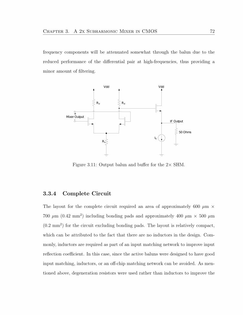
Chapter 3. A 2x Subharmonic Mixer in CMOS 72
frequency components will be attenuated somewhat through the balun due to the
reduced performance of the differential pair at high-frequencies, thus providing a
minor amount of filtering.
Figure 3.11: Output balun and buffer for the 2× SHM.
3.3.4 Complete Circuit
The layout for the complete circuit required an area of approximately 600 µm ×
700 µm (0.42 mm2) including bonding pads and approximately 400 µm × 500 µm
(0.2 mm2) for the circuit excluding bonding pads. The layout is relatively compact,
which can be attributed to the fact that there are no inductors in the design. Com-
monly, inductors are required as part of an input matching network to improve input
reflection coefficient. In this case, since the active baluns were designed to have good
input matching, inductors, or an off-chip matching network can be avoided. As men-
tioned above, degeneration resistors were used rather than inductors to improve the

Chapter 3. A 2x Subharmonic Mixer in CMOS 73
linearity, but require significantly less space on the integrated circuit. A photograph
of the fabricated chip is shown in Figure 3.12.
Figure 3.12: Photograph of fabricated CMOS 2× subharmonic mixer.
3.4 Measurement Results
To measure the subharmonic mixer, coplanar waveguide probes were used to contact
the on-chip pads and a Rohde and Schwarz FS300 spectrum analyzer was used to
measure the power spectrum of the output signal. The spectrum analyzer was set to
a frequency span of 50 MHz to 150 MHz with a resolution bandwidth (RBW) and
a video bandwidth (VBW) both equal to 1 MHz, and continuous sweeping with a
sweep time of 25 ms. Averaging was not used for any measurements and no internal
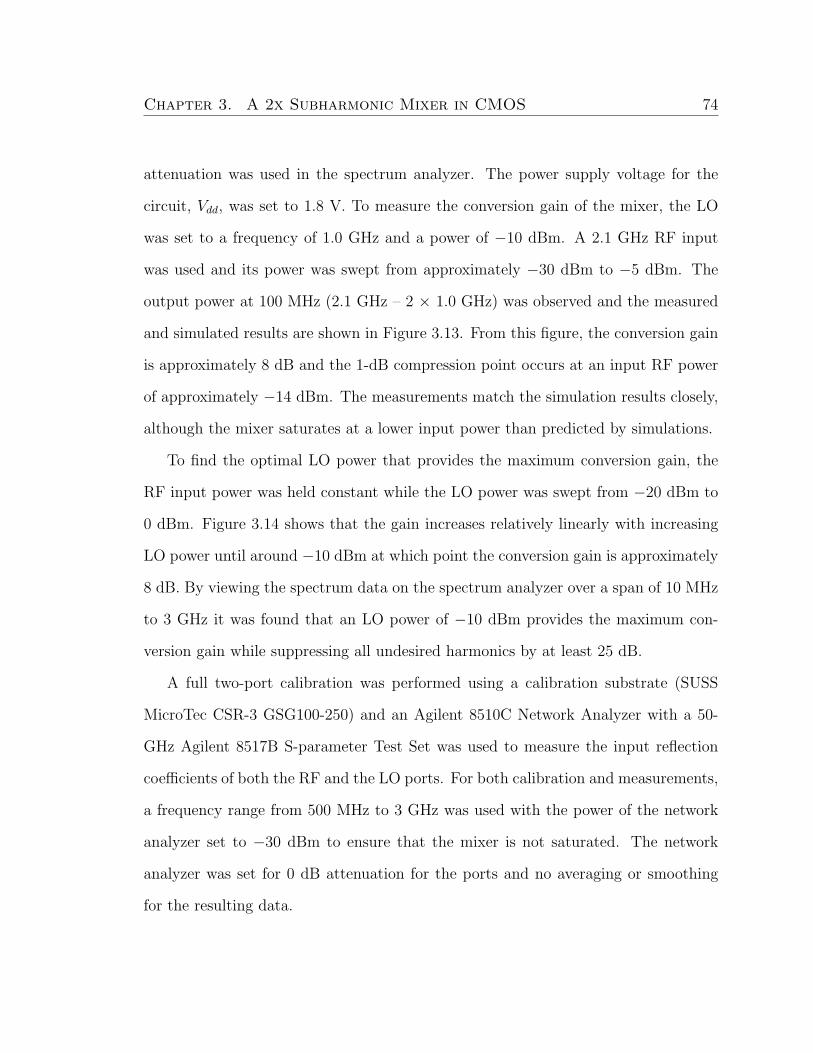
Chapter 3. A 2x Subharmonic Mixer in CMOS 74
attenuation was used in the spectrum analyzer. The power supply voltage for the
circuit, Vdd, was set to 1.8 V. To measure the conversion gain of the mixer, the LO
was set to a frequency of 1.0 GHz and a power of −10 dBm. A 2.1 GHz RF input
was used and its power was swept from approximately −30 dBm to −5 dBm. The
output power at 100 MHz (2.1 GHz – 2 × 1.0 GHz) was observed and the measured
and simulated results are shown in Figure 3.13. From this figure, the conversion gain
is approximately 8 dB and the 1-dB compression point occurs at an input RF power
of approximately −14 dBm. The measurements match the simulation results closely,
although the mixer saturates at a lower input power than predicted by simulations.
To find the optimal LO power that provides the maximum conversion gain, the
RF input power was held constant while the LO power was swept from −20 dBm to
0 dBm. Figure 3.14 shows that the gain increases relatively linearly with increasing
LO power until around −10 dBm at which point the conversion gain is approximately
8 dB. By viewing the spectrum data on the spectrum analyzer over a span of 10 MHz
to 3 GHz it was found that an LO power of −10 dBm provides the maximum con-
version gain while suppressing all undesired harmonics by at least 25 dB.
A full two-port calibration was performed using a calibration substrate (SUSS
MicroTec CSR-3 GSG100-250) and an Agilent 8510C Network Analyzer with a 50-
GHz Agilent 8517B S-parameter Test Set was used to measure the input reflection
coefficients of both the RF and the LO ports. For both calibration and measurements,
a frequency range from 500 MHz to 3 GHz was used with the power of the network
analyzer set to −30 dBm to ensure that the mixer is not saturated. The network
analyzer was set for 0 dB attenuation for the ports and no averaging or smoothing
for the resulting data.

Chapter 3. A 2x Subharmonic Mixer in CMOS 75
−30 −25 −20 −15 −10 −5 0−25
−20
−15
−10
−5
0
RF Input Power (dBm)
IF O
utpu
t Pow
er (
dBm
)
LO Power = −10 dBm
Simulated
Measured
Figure 3.13: Measured and simulated 1-dB compression point.
−20 −18 −16 −14 −12 −10 −8 −6 −4 −2 0−10
−5
0
5
10
15
LO Input Power (dBm)
Con
vers
ion
Gai
n (d
B)
RF Power = −20 dBm
Simulated
Measured
Figure 3.14: Measured and simulated conversion gain at various LO power levels.

Chapter 3. A 2x Subharmonic Mixer in CMOS 76
The S11 for the RF input is shown in Figure 3.15. It is clear that the active input
balun provides good matching with an input reflection coefficient less than −10 dB
at 2.1 GHz. Similarly, the LO input reflection coefficient, shown in Figure 3.16, is
approximately −11 dB at the LO frequency of 1.0 GHz. The slight difference between
the RF and the LO input matching is due to minor differences in the active balun
circuits that allows a lower input reflection coefficient at the operational frequency of
the LO at the expense of higher power consumption. The third-order intercept point
(IP3) was measured by using a two-tone RF input signal with frequencies of 2.1 GHz
and 2.11 GHz. This produced third-order intermodulation products at 90 MHz and
120 MHz. The results shown in Figure 3.17 indicate an IIP3 of −8.5 dBm and an
OIP3 of −0.5 dBm. The IP2 was simulated using the same two-tone RF input signals
at the IP3 measurement (2.1 GHz and 2.11 GHz), which produces an IM2 component
at 10 MHz. Simulations show an IIP2 of 14 dBm including the output balun circuit,
and an IIP2 of over 30 dBm using an ideal output balun (i.e. the IIP2 of the mixer
alone is over 30 dBm).
The port-to-port isolation was simulated using ADS in order to determine the
isolation between the mixer ports without the effects of the input or output baluns.
The results, tabulated in 3.1, show very high-levels of isolation such as 68 dB for
the 2LO–RF feedthrough. Clearly, this will be very beneficial in direct-conversion
applications since the high 2LO–RF isolation will result in low LO self-mixing.
The noise figure of the mixer was measured using an Agilent 346C noise source
along with the Noise Figure Measurement Personality of the Agilent E4446A PSA
Series spectrum analyzer. A calibration was first performed, and the resolution band-
width was set to 1 MHz. The measured double sideband (DSB) noise figure is 20 dB.

Chapter 3. A 2x Subharmonic Mixer in CMOS 77
0.5 1 1.5 2 2.5 3−15
−10
−5
0
RF Frequency (GHz)
RF
Inpu
t Ref
lect
ion
Coe
ffici
ent (
dB)
Figure 3.15: Measured RF input reflection coefficient for the 2× SHM.
0.5 1 1.5 2 2.5 3−15
−10
−5
0
LO Frequency (GHz)
LO In
put R
efle
ctio
n C
oeffi
cien
t (dB
)
Figure 3.16: Measured LO input reflection coefficient for the 2× SHM.

Chapter 3. A 2x Subharmonic Mixer in CMOS 78
−30 −25 −20 −15 −10 −5 0−50
−45
−40
−35
−30
−25
−20
−15
−10
−5
0
5
RF Input Power (dBm)
IF O
utpu
t Pow
er (
dBm
)IP3
LO Power = −10 dBm
Fundamental
3rd Order Intermodulation Products
Figure 3.17: Third-order intercept point measurement for the 2× SHM.
Ports Isolation
RF–LO 62 dB
LO–RF 58 dB
2LO–RF 68 dB
RF–IF 35 dB
LO–IF 37 dB
2LO–IF 49 dB
Table 3.1: 2× subharmonic mixer port-to-port isolation simulations.

Chapter 3. A 2x Subharmonic Mixer in CMOS 79
Technology fRF /fLO Gain P-1dB IIP3 DC Power Ref.(GHz) (dB) (dBm) (dBm) (mW)
BiCMOS 1.9/0.9 7.5 −8 −3 24 [36]0.35 µm
SiGe BiCMOS 5.6/2.8 8.0 −13.5 0 4.67 [87]*0.18 µmCMOS 5.6/2.8 8.0 −12 −6.5 5.25 [89]*
0.25 µmCMOS 2.1/1.0 8.0 −14 −8.5 364 This Work
0.18 µm [8]
* Simulation results only4 Includes balun circuits
Table 3.2: 2× subharmonic mixer circuit performance comparison.
The noise figure could be reduced by modifying the input baluns to eliminate the bias
resistor Rb, or by using another balun topology. The power consumption for the cir-
cuit, including input and output baluns, the mixer core, as well as the output buffer,
is 36 mW (the power consumption of the mixer core alone is approximately 1 mW).
A comparison of this work with other subharmonic mixers of this type ([36, 87, 89]),
is presented in Table 3.2. Note that in these references that they do not use on-chip
baluns, and in the case of [87] and [89] only simulation results are shown.
3.5 Summary
In this chapter, a CMOS 0.18 µm 2× subharmonic mixer was demonstrated that uses
active input and output baluns to generate differential signals from single-ended, and
vice-versa. This configuration could be used as part of a direct-conversion receiver
where single-ended inputs and outputs are required or in a superheterodyne receiver

Chapter 3. A 2x Subharmonic Mixer in CMOS 80
where a lower LO frequency is desired. By using a 2× subharmonic mixer, the
LO frequency is designed to have half the frequency that would be required with a
fundamental mixer. Consequently, the design of the LO can possibly be simplified
and improved performance can result due to the reduced oscillation frequency. The
RF input frequency was 2.1 GHz and the LO frequency was 1.0 GHz, which results
in an output IF of 100 MHz. Active baluns at the RF and LO input ports were
designed to have active input matching and the measured results show input reflection
coefficients of less than −10 dB at the LO and RF operational frequencies. The 1-
dB compression point was found to occur at −14 dBm RF input power and the
conversion gain was approximately 8 dB. If a quadrature oscillator is used for the
LO, such as the one described in Chapter 5 of this dissertation, it could eliminate
the need for the passive RC–CR phase-shifters and the LO balun, and potentially
improve performance through increased phase accuracy.

Chapter 4
A CMOS Ku-Band 4x
Subharmonic Mixer
4.1 Introduction
In this chapter, a novel 4× subharmonic mixer is presented using CMOS technology
that is a significant extension of the 2× SHM described in the previous chapter [6].
An RF frequency in the Ku-band (12 GHz) was used to demonstrate this circuit,
which is a very commonly used band for satellite communications. To the best of the
author’s knowledge, this is the first 4× subharmonic mixer demonstrated in CMOS
technology. Furthermore, it obtains a conversion gain of 6 dB, which is the highest
conversion gain for any 4× SHM to date.
Although it is possible to realize an LO that operates directly at Ku-band in CMOS
technology, the resulting fundamental mixer would likely have increased self-mixing
and therefore degrade the performance of a direct-conversion receiver compared to
a subharmonic mixer. Similarly, while it would be possible to use a separate LO
81

Chapter 4. A CMOS Ku-Band 4x Subharmonic Mixer 82
frequency multiplier along with a fundamental or a 2× SHM, the resulting power
consumption and required chip area could potentially increase and the port-to-port
isolation could suffer, resulting in an increase in self-mixing. The proposed circuit
could easily be moved to higher frequencies (mm-wave) where subharmonic mixing
may be a necessity, and in this regard it can be viewed as a lower frequency demon-
stration circuit.
4.2 Concept of the 4x Subharmonic Mixer
The core of the 4× SHM is based on the Gilbert-cell topology [17]. As shown in
Figure 4.1, the proposed SHM has the RF and LO ports exchanged compared to a
traditional Gilbert-cell. Furthermore, the two transistors typically at the bottom of
the Gilbert-cell have been replaced by two sets of four transistors that will generate
the fourth harmonic of the LO signal, thus allowing the mixer to operate as a 4×
SHM. The inputs to these transistors are octet-phase LO signals, with 0, 90, 180,
and 270 applied to the gates of one set of four FETs and 45, 135, 225, 315 applied
to the gates of the other set of FETs. In other 2× SHM circuits (e.g. [8, 32, 36])
a similar topology is used, but with two pairs of LO transistors instead of four, and
they use only quadrature LO signals.

Chapter 4. A CMOS Ku-Band 4x Subharmonic Mixer 83
Rbias
VDD VDD
180o
0o
90o
180o
270o
225o
315o
45o
135o
Rm Rm
L L
Out 0o
Out 180o
LOInputs
RFInputs
0o
vSHM 0 vSHM 180
Figure 4.1: The mixer core of the proposed 4× SHM.

Chapter 4. A CMOS Ku-Band 4x Subharmonic Mixer 84
4.3 Circuit Design
4.3.1 Mixer Core
To examine the operation of the mixer, consider one set of four transistors, as shown
in Figure 4.2a, with LO signals applied to the gates with relative phase shifts of 0,
90, 180, 270, as shown in Figure 4.2b. The four quadrature LO signals applied
to the gates generate a 4fLO signal, as opposed to differential gate signals which
only generate a 2fLO signal as in [8, 32, 36]. The quadrature signals applied to the
gates of the other set of four transistors are shifted by 45. This topology generates
a 4fLO signal that is 180 out of phase with the other 4fLO signal. Therefore, this
mixer topology is double-balanced, which allows this topology to achieve high-levels
of isolation between the ports. If the LO signals have a DC bias at the transistor
threshold voltage, Vt, the signals are given by:
vLO0 = ALOcos(ωLOt) + Vt
vLO90 = ALOcos(ωLOt− π/2) + Vt
vLO180 = ALOcos(ωLOt− π) + Vt
vLO270 = ALOcos(ωLOt− 3π/2) + Vt
where ALO is the amplitude of the LO signal. If it is assumed that the transistors are
completely cutoff when the gate voltage is below the threshold voltage (i.e. ignoring
sub-threshold current), the LO0 and LO180 pair of transistors can be modeled by one
transistor with LO gate voltage of,
v0,180 = |ALOcos(ωLOt)|+ Vt (4.1)
since only one of the two transistors is on during each half-cycle. Clearly, this wave-
form contains the double frequency, or second harmonic. Similarly, the LO90 and

Chapter 4. A CMOS Ku-Band 4x Subharmonic Mixer 85
0o
90o
180o
270o
L
Rbias
Vth t
v =|cos( t)|
L
Rbias
Vth t Vth t
iT
i0,180 i90,270
iT
v90,270v0,180
freq = 4fLO
freq = fLO
freq = 2fLO freq = 2fLO
t
iT
(a) (b)
(c)
o
0,180v =|cos( t-90 )|90,270
vd
vx
vd
vx
Vth
Figure 4.2: (a) One of the two 4× LO generation circuits, (b) Quadrature LO time-domain signals, and (c) Modeling the 4× LO circuit.

Chapter 4. A CMOS Ku-Band 4x Subharmonic Mixer 86
LO270 transistors can be replaced by one transistor with LO gate voltage of,
v90,270 = |ALOcos(ωLOt− π/2)|+ Vt (4.2)
This model is shown in Figure 4.2c. Using the short-channel model, the currents
generated by the LO voltages are given by:
i0,180 =WCoxVsat(v0,180 − Vt)
1 + LEsat/(v0,180 − Vt)(4.3)
i90,270 =WCoxVsat(v90,270 − Vt)
1 + LEsat/(v90,270 − Vt)(4.4)
To simplify the analysis and to clearly see the generation of the fourth harmonic,
the approximation can be made that (vgs − Vt)/L is large compared to Esat such
that the denominator 1 + LEsat/(Vgs − Vt) ≈ 1. A numerical analysis shows that
when the amplitude of the gate signal, ALO, is large, the results of the simplified
equations based on this approximation are very close to the results obtained using
(4.3) and (4.4). Since the LO signal amplitude will generally be large, it follows that
this assumption is reasonable for this circuit. The benefit of using the simplified drain
current formula is that more insight can be obtained from the resulting equations.
With this approximation, the drain currents are given by:
i0,180 ≈1
2µnCoxWEsat|ALOcos(ωLOt)| (4.5)
i90,270 ≈1
2µnCoxWEsat|ALOcos(ωLOt− π/2)| (4.6)
The total current, iT , is simply given by iT = i0,180 + i90,270, therefore,
iT ≈1
2µnCoxWEsatALO(|cos(ωLOt)|+ |sin(ωLOt)|) (4.7)

Chapter 4. A CMOS Ku-Band 4x Subharmonic Mixer 87
Since,
|cos(ωt)|+ |sin(ωt)| =√|sin(2ωt)|+ 1 (4.8)
the following Taylor series expansion can be applied,
√x+ 1 =
∞∑n=0
(−1)n(2n)!
(1− 2n)(n!)24nxn |x| ≤ 1 (4.9)
Therefore, iT expanded to three terms is given by,
iT ≈1
2µnCoxWEsatALO
(15
16+
1
2|sin(2ωLOt)|+
1
16cos(4ωLOt)
). (4.10)
The two terms |sin(2ωLOt)| and cos(4ωLOt) both clearly show the fourth harmonic.
The total output current signal, iT , is dominated by the |sin(2ωLOt)| term since
its frequency component at 4fLO is over three times stronger than the 116cos(4ωLOt)
component. The crucial result is that the frequency of the output current is at
four times the input LO frequency, or, 4fLO, as desired. A similar analysis can be
performed on the other set of four transistors to show the generation of the fourth
harmonic and the anti-phase relationship with (4.10). Since the mixer core maintains
a differential structure, the common-mode rejection will be high and similar to that
of the traditional Gilbert-cell. Of course, a disadvantage to this topology is that a
higher LO input power will be required compared to a fundamental mixer since there
is conversion loss in the 4× LO frequency multiplication circuit.
The purpose of the inductors in the mixer core (Figures 4.1 and 4.2a) are to
increase the LO voltage swing at the source terminal of the RF transistors as discussed
in [26], which ultimately provides higher conversion gain for the mixer at lower LO
powers than would be required without the enhancement inductors. The voltage at
node vx shown in Figure 4.2a is given by,

Chapter 4. A CMOS Ku-Band 4x Subharmonic Mixer 88
vx = vd + (Rind + jωLOL)iT (4.11)
where vd is the common drain node of the LO transistors as shown in Figure 4.2a, and
Rind and L are the series resistance and the inductance of the on-chip spiral inductor,
respectively. Since the desired LO frequency is four times the LO input frequency,
this inductor provides a large impedance, which increases the voltage swing at vx and
improves the resulting conversion gain. It also provides filtering for any parasitic fLO
and 2fLO signals that are present since the impedance of the inductor is lower for these
signals. It is also possible to trade conversion gain for linearity by using degeneration
resistors or inductors in the sources of the RF transistors. In this implementation of
the 4× SHM the goal was maximum conversion gain, and therefore degeneration was
not used.
4.3.2 Input RF Balun
In some cases, single-ended signals are used as opposed to balanced signals. In order
to convert the single-ended RF signal to a balanced signal, an active balun was used
in this work primarily for ease of testing. The use of an active balun as opposed to
a passive balun enables this circuit to be conveniently implemented on chip since the
required size is vastly reduced. The topology of the active balun used is shown in
Figure 4.3. The circuit uses a common-source path to produce a 180 phase shift and a
common-gate path to produce the 0 signal with equal amplitudes [91]. An advantage
to this technique is the ability to achieve a reasonably good input impedance match to
50 Ω since the input to this balun is approximately that of the common-gate circuit,
Zin ≈ 1/gm (the resistor Rb is large). Therefore, with appropriate selection of device

Chapter 4. A CMOS Ku-Band 4x Subharmonic Mixer 89
Rb
v
v
0
180
RF Input
Rb1
VDD VDD
Rb2
VDD
Figure 4.3: RF active balun circuit for the 4× SHM.
size and biasing, the input of the balun can produce wideband matching. While
this topology may be somewhat more sensitive to fabrication process variations than
a differential pair configuration, the elimination of matching inductors that would
likely be required with a differential pair balun saves significant chip area.
Simulation results of the active balun at an input frequency around 12 GHz show
that the phase error is approximately 6 and the amplitude imbalance is approxi-
mately 0.5 dB. The voltage loss through the balun at 12 GHz when the load is the
input to the SHM is −3 dB. Obviously, if a balanced RF signal was already available
then the RF balun would not be necessary and the resulting conversion gain would
be increased. Since the RF signal is not perfectly balanced, the RF–IF isolation may
be degraded somewhat. However, since the RF frequency is in the Ku-band and the

Chapter 4. A CMOS Ku-Band 4x Subharmonic Mixer 90
IF frequency is quite low, this should not pose a significant problem since it could
easily be removed by a simple filter.
4.3.3 LO Phase Shifters
In order to realize the 4× SHM discussed in the previous section, octet-phase LO
signals are required. Octet-phase LO signals were also required in the SHMs presented
in [29–31, 35], however, all of these circuits were only 2× SHMs. RC–CR polyphase
filters were used to generate the required phase shifts in [15]. This technique, although
the simplest, can generate phase and amplitude errors due to fabrication tolerances
in the resistors. Similarly, the 45 phase shifter in [35] was also a passive network
consisting of resistors and capacitors. The technique used to generate the octet signals
in this work is similar to the technique used in [29]. This method essentially uses an
active summer to add a 0 and a 90 signal to realize a 45 signal,
Acos(ωt) + Acos(ωt+ π/2) =√
2Acos(ωt+ π/4). (4.12)
This 45 phase shift is relative to a similar in-phase (0) adder circuit that adds
two signals with the same phase. The purpose of the in-phase adder is to equalize
parasitics in the two paths so that a more accurate 45 phase relationship can be
obtained. The circuit schematics of the 45 phase shifter and the in-phase adder are
shown in Figure 4.4. By the proper scaling of resistors, R45 and R0, the amplitudes of
the 45 phase shifter and the in-phase adders can be made equal and can potentially
achieve conversion gain (in this implementation there was a small conversion loss).
Since there is a total of eight in-phase and 45 phase shifter circuits, there may be
a significant increase in DC power consumption. Passive 45 phase shifter circuits
could be used for low-power applications.

Chapter 4. A CMOS Ku-Band 4x Subharmonic Mixer 91
VDD
R45
0o
Vbias
90o
v45
VDD
R0
0o
v0
0
90
180
270
45
o
o
o
o
o
Vbias
Figure 4.4: 45 phase shifter circuit. 0 and 90 signals are added producing a signalat v45 that is 45 out of phase with the output of the in-phase adder, v0.
Clearly, to use the aforementioned technique, quadrature LO signals must be
available. In many cases, this is not a problem since a quadrature oscillator can
simply be used. To verify the proposed 4× SHM in this work, a differential LO input
signal was used along with a passive RC–CR 90 phase shifter, as shown in Figure
4.5. Simulation results on the complete octet-phase generator circuit show a phase
error of approximately 1 and a amplitude imbalance of less than 1 dB using this
technique. The main concern with using this technique is that the tolerance in the
various components in the fabrication process can lead to larger phase and amplitude
errors than are shown in simulations (particularly in the RC–CR 90 phase shifters)
and the resulting mixer performance will be degraded. A detailed analysis of the
effects of potential phase and amplitude errors using this technique were presented
in [29]. It was found that by following the polyphase filter with the active 45 phase

Chapter 4. A CMOS Ku-Band 4x Subharmonic Mixer 92
v-45
v45
LO0
R1
C1
R1
C1
v135
v225
LO180
R1
C1
R1
C1
Figure 4.5: 90 RC–CR phase shifter used in the 4× SHM.
shifting circuit shown in Figure 4.4 the resulting octet-phase outputs are actually
desensitized to phase errors in the polyphase filters. Furthermore, it was determined
that even with significant process variations of the resistance in the RC–CR 90 phase
shifters the resulting accuracy of the octet-phase signal was still within acceptable
limits [29].
4.3.4 Output Balun
In order to convert the differential amplifier output back to single-ended for mea-
surement, another active balun was used. Since the IF output will be at a relatively
low frequency (100 MHz, in this case), it makes the use of an active balun very
attractive compared to passive techniques, given the large wavelength of the sig-
nal. Furthermore, since the frequency is low, it makes the design of this balun very

Chapter 4. A CMOS Ku-Band 4x Subharmonic Mixer 93
VDD VDD
Rd Rd
VDD
Rload50 Ohms
I1
I2
CbvSHM 0 vSHM 180vOUT
Figure 4.6: Output balun circuit for the 4× SHM.
straight-forward. The output balun is shown in Figure 4.6 which includes a differen-
tial pair with a single-ended output that is connected to a source-follower buffer. The
output balun was designed such that the differential voltage amplitude at the mixer
output equals the buffer output, vSHM0 − vSHM180 = vOUT . Therefore, there was no
gain in this stage that would contribute to the conversion gain of the mixer.
4.4 Measurement Results
To characterize the 4× CMOS SHM, coplanar waveguide (CPW) probes were used
for on-chip probing. An Agilent E4446A PSA Series spectrum analyzer was used to
observe the output spectrum of the mixer. The DC supply voltage was set to 2.75 V,
the RF input signal was −20 dBm at 12.1 GHz, and the LO signal was 10 dBm at

Chapter 4. A CMOS Ku-Band 4x Subharmonic Mixer 94
3.0 GHz. Therefore, the desired IF output signal was at 100 MHz (fRF − 4fLO).
The mixer output spectrum was measured with the state of the spectrum analyzer as
follows: a frequency span from 1 MHz to 15 GHz, RBW and VBW equal to 3 MHz,
10 dB internal attenuation, average of 10 sweeps, 601 points, and 30 ms sweep time.
The output spectrum is shown in Figure 4.7. The conversion gain is approximately
5.8 dB and all other spectral components are below −45 dBm (more than 30 dB
below the IF).
To measure the 1-dB compression point, the gain at various LO input power
levels, the IP3, and the IP2, the settings on the spectrum analyzer were adjusted to
the following: a frequency span from 1 MHz to 150 MHz, RBW and VBW equal to
1.5 MHz, 10 dB internal attenuation, 10-point averaging, 601 points, and 1 ms sweep
time. In order to determine the 1-dB compression point of the mixer, the input
0 1 2 3 4 5 6 7 8 9 10 11 12 13 14 15−80
−70
−60
−50
−40
−30
−20
−10
0
Frequency (GHz)
Out
put P
ower
(dB
m)
RF Input: −20 dBm @ 12.1 GHzLO Input: 10 dBm @ 3.0 GHzIF Output
Figure 4.7: Measured mixer output spectrum with −20 dBm RF power and 10 dBmLO power.

Chapter 4. A CMOS Ku-Band 4x Subharmonic Mixer 95
power was swept and the IF output power was measured. The measurement and
simulation results are shown in Figure 4.8. The measured input 1-dB compression
point is −12 dBm. The simulation results are very similar to the measured results,
however, the measurements show an earlier saturation than in simulation. The 1-
dB compression point would be improved somewhat if a differential RF input signal
was fed directly to the mixer without going through the balun circuit. Nevertheless,
an input P1dB of −12 dBm is very similar to the subharmonic mixers reported in
[24, 25, 28, 29, 37, 41, 42].
A plot of the conversion gain at various LO input power levels is shown in Figure
4.9. From this figure, conversion gain is achieved when the LO power is above 8.4 dBm
with a maximum conversion gain of approximately 6.5 dB occurring at 11 dBm LO
input power. An optimal conversion gain was determined to occur for an LO input
−25 −20 −15 −10 −5−20
−18
−16
−14
−12
−10
−8
−6
−4
−2
0
RF Input Power (dBm)
IF O
utpu
t Pow
er (
dBm
)
SimulatedMeasured
Figure 4.8: 1-dB compression point measurement (LO power = 10 dBm).

Chapter 4. A CMOS Ku-Band 4x Subharmonic Mixer 96
5 6 7 8 9 10 11 12 13−25
−20
−15
−10
−5
0
5
10
LO Input Power (dBm)
Con
vers
ion
Gai
n (d
B)
Figure 4.9: Conversion gain at various LO power levels for the 4× SHM.
power of 10 dBm while still having very strong suppression of undesired spectral
components (more than 30 dB below the IF). Note that these conversion gain values
were obtained while having a 3 dB loss through the RF balun, and therefore higher
conversion gains would be possible if a differential RF signal is already available.
A conversion gain of approximately 6 dB is the highest that could be found in the
literature for a 4× SHM, e.g. [38–43] (most of which exhibit a conversion loss).
The possibility of a lower RF interfering signal mixing with a subharmonic of the
LO was also considered. For example, a 6.1 GHz RF interfering signal could mix with
the 2× LO component at 6 GHz, which would interfere with the desired IF signal.
From the Taylor series expansion of the LO signal in Equation (4.10), there is, ideally,
no component at 2fLO, so the conversion gain from a 6.1 GHz RF to a 100 MHz IF
should be very low (ideally zero). Simulations show that this conversion gain is 40 dB

Chapter 4. A CMOS Ku-Band 4x Subharmonic Mixer 97
below that of the desired mixing products, and therefore this is not a serious concern
(in addition there would likely be an RF filter that would attenuate out of band RF
signals anyway).
The third-order intercept point and the second-order intercept point were mea-
sured to determine the linearity of the mixer. To measure the IP3, a two-tone RF
signal was applied at 12.10 GHz and 12.11 GHz (LO power was 10 dBm at 3.0 GHz).
This produced third-order distortion signals at 90 MHz and 120 MHz. The results
are shown in Figure 4.10. The IIP3 is approximately −2 dBm and the OIP3 is ap-
proximately 4 dBm. Simulations were also performed to determine the maximum
IIP3 that could be obtained if source degeneration resistors were used in the sources
of the RF transistors to improve linearity. It was found that an IIP3 of over 10 dBm
could be achieved while maintaining a conversion gain of 0 dB.
To determine the IP2, the same two RF tones were applied (12.10 GHz and
12.11 GHz), but the spectral component at 10 MHz was observed as the RF input
power increased. The plot of this measurement is shown in Figure 4.11. The IIP2 was
determined to be approximately 17 dBm. It was found through simulations that the
output active balun seriously degrades the IP2. Simulations with an ideal IF output
balun show that the IP2 is increased by 14 dB, and therefore, the IIP2 of the mixer
itself is greater than 30 dBm.
The input reflection coefficient to the RF port was also measured using an Agilent
8510C Network Analyzer with a 50 GHz Agilent 8517B S-parameter Test Set. Cal-
ibration of the network analyzer was performed using a calibration substrate (SUSS
MicroTec CSR-3 GSG100-250). The network analyzer was calibrated from 1 GHz to
15 GHz with 401 points and the port power levels were both set to −30 dBm. No

Chapter 4. A CMOS Ku-Band 4x Subharmonic Mixer 98
−30 −25 −20 −15 −10 −5 0−80
−70
−60
−50
−40
−30
−20
−10
0
10
20
RF Input Power (dBm)
Out
put P
ower
(dB
m)
Fundamental
IP3
3rd Order Intermodulation Products
Figure 4.10: Third-order intercept point measurement (LO power = 10 dBm).
−30 −25 −20 −15 −10 −5 0 5 10 15 20−70
−60
−50
−40
−30
−20
−10
0
10
20
30
RF Input Power (dBm)
Out
put P
ower
(dB
m)
IP2
Fundamental
2nd Order Intermodulation Products
Figure 4.11: Second-order intercept point measurement (LO power = 10 dBm).

Chapter 4. A CMOS Ku-Band 4x Subharmonic Mixer 99
internal network analyzer attenuation was used and no averaging or smoothing was
performed on the measured data.
The measured S11 is shown in Figure 4.12. Due to the common-gate device in the
RF balun there is relatively wideband input matching. The input reflection coefficient
is better than −10 dB between 10 GHz and 15 GHz.
To evaluate the susceptibility of the proposed SHM topology to DC offsets, the
procedure discussed in [15] was used. Specifically, the DC level at the output was
measured with three different setups: 1) Under DC bias only (RF and LO signals
not applied), 2) DC bias and LO signal applied (no RF signal), and 3) DC bias with
the LO signal and RF input. While performing the measurement in Step 1) both
the RF and LO ports were terminated in 50 Ω loads and in Step 2) the RF port
was terminated in a 50 Ω load. The difference between the measured DC output
2 4 6 8 10 12 14−12
−10
−8
−6
−4
−2
0
Frequency (GHz)
RF
S11
(dB
)
Figure 4.12: Measured RF input reflection coefficient for the 4× SHM.

Chapter 4. A CMOS Ku-Band 4x Subharmonic Mixer 100
Ports Isolation
RF–LO 43 dB
LO–RF 71 dB
2LO–RF 52 dB
4LO–RF 59 dB
RF–IF 30 dB
LO–IF 68 dB
2LO–IF 55 dB
4LO–IF 59 dB
Table 4.1: 4× subharmonic mixer port-to-port isolation measurements.
values in Steps 1) and 2) indicate the amount of LO self-mixing. In the case of
the proposed 4× SHM, this value was measured to be 4.2 mV at an LO power of
10 dBm. The measurement in Step 3) includes the effects of the DC offsets produced
by second-order nonlinearities. The measured DC offset for this case was 1.2 mV.
The isolation between the ports of the mixer was measured and the results are
compiled in Table 4.1. Very high isolations between the ports were measured, with
all isolations being greater than 43 dB with the exception of the RF–IF isolation
(30 dB), which is predominately due to the amplitude and phase imbalance from the
RF balun. The LO–RF and the 4LO–RF suppressions, in particular are very high at
71 dB and 59 dB, respectively. These isolation measurements are very competitive and
in most cases improvements over previous SHMs (e.g. [21, 25, 27, 29, 33, 38, 42, 43]).
The noise figure for the entire circuit was measured using the Noise Figure Mea-
surement Personality of the Agilent E4446A PSA Series spectrum analyzer along
with an Agilent 346C noise source. A noise figure calibration was first performed by

Chapter 4. A CMOS Ku-Band 4x Subharmonic Mixer 101
connecting the noise source directly to the spectrum analyzer input. The resolution
bandwidth of the spectrum analyzer was 1 MHz for the noise figure measurement.
The double sideband (DSB) noise figure was measured to be 15 dB (SSB NF≈ 18 dB),
which includes the noise generated in the input RF balun. To determine the noise
of the mixer alone, simulations were performed with an ideal input RF balun and
the results show that the noise figure decreased by approximately 3 dB. Therefore, if
a differential RF is already available, the DSB noise figure would be approximately
12 dB, which is similar to, or an improvement upon, the subharmonic mixers de-
scribed in [24, 26–28, 33, 34, 37]. Flicker noise measurements were not performed
due to an output DC-blocking capacitor. It is expected that the flicker noise will be
increased somewhat compared to the traditional Gilbert-cell due to the additional
LO switching noise, as discussed in [94].
The DC power consumption for the mixer core was approximately 5 mW and
for the entire chip including the RF balun, LO octet-phase generation, mixer core,
output balun, and buffer, the power consumption was measured to be 113 mW. The
simulated power consumption for the octet-phase generation circuit and the mixer
core alone is approximately 50 mW. The chip dimensions were 850 µm × 850 µm
including pads. A photograph of the fabricated chip is shown in Figure 4.13.
4.5 Summary
A new 4× subharmonic mixer has been presented using CMOS 0.18 µm technology
that accepts a 12.1 GHz RF input signal and a 3.0 GHz LO signal and produces a
100 MHz IF output (fRF − 4fLO). The circuit requires octet-phase LO signals, which
are generated in this work through a polyphase filter and an active 45 phase shifting

Chapter 4. A CMOS Ku-Band 4x Subharmonic Mixer 102
Figure 4.13: Microphotograph of the proposed 4× SHM.
circuit. An active balun was used for the RF port to convert the single-ended 12.1 GHz
signal to a differential signal and another active balun is used at the output to convert
the differential output signal back to single-ended for measurement. A conversion gain
of approximately 6 dB and a 1-dB compression point of −12 dBm was obtained. Very
high isolations between the ports were measured with LO–RF isolation of 71 dB and
4LO–RF isolation of 59 dB. The measured IIP3 and IIP2 were −2 dBm and 17 dBm,
respectively. The circuit dimensions are 850 µm × 850 µm. To the best of the
author’s knowledge, this is the first 4× subharmonic mixer demonstrated in CMOS
technology and it achieves the highest conversion gain for any 4× SHM to date. This
circuit could be used to reduce the LO self-mixing in a direct conversion receiver, or
in any mixer application where the reduction of the local oscillator frequency by a
factor of four is beneficial.

Chapter 5
Quadrature Oscillator
5.1 Introduction
In this Chapter a quadrature oscillator is presented that uses superharmonic coupling
[9]. This quadrature oscillator is suitable for use with both the 2× subharmonic mixer
discussed in Chapter 3, as well as the 4× subharmonic mixer discussed in Chapter 4.
The presence of harmonics in CMOS oscillator circuits is unavoidable. These
harmonics are generally unwanted signals that appear with the desired fundamen-
tal signal. In differential oscillators there exist common-mode nodes (like the two
source nodes in a cross-coupled oscillator) where higher-order harmonics are present
and the fundamental is essentially absent. These second-order harmonics present at
the common-mode nodes of two oscillators can be used to enforce a quadrature rela-
tionship between the fundamental outputs through a technique called superharmonic
coupling.
103
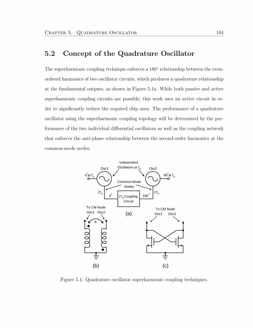
Chapter 5. Quadrature Oscillator 104
5.2 Concept of the Quadrature Oscillator
The superharmonic coupling technique enforces a 180 relationship between the even-
ordered harmonics of two oscillator circuits, which produces a quadrature relationship
at the fundamental outputs, as shown in Figure 5.1a. While both passive and active
superharmonic coupling circuits are possible, this work uses an active circuit in or-
der to significantly reduce the required chip area. The performance of a quadrature
oscillator using the superharmonic coupling topology will be determined by the per-
formance of the two individual differential oscillators as well as the coupling network
that enforces the anti-phase relationship between the second-order harmonics at the
common-mode nodes.
CouplingCircuit
IndependentOscillators at f0
2 00 180
o o
(a)
(c)(b)
Common-ModeNodes
K
To CM NodeOsc1 Osc2
To CM NodeOsc1 Osc2
Osc1 Osc2
0 ato
f0 90 ato
f0
f2 0f2 0f
Figure 5.1: Quadrature oscillator superharmonic coupling techniques.

Chapter 5. Quadrature Oscillator 105
5.3 Circuit Design
A very common way of implementing a CMOS differential LC oscillator is to use
a cross-coupled pair to generate the negative resistance required to overcome the
losses in the tank. The resistance looking into the cross-coupled pair is given by
−2/gm where gm is the transconductance of each of the FETs in the cross-coupled
pair. Therefore, with an appropriate device size and biasing, the negative resistance
required to counteract the losses in the tank can be realized.
The core quadrature oscillator circuit investigated in this work is shown in Figure
5.2. It consists of two cross-coupled oscillators connected through a cross-coupled
pair. It has been shown that by including cross-coupled PMOS transistors above the
cross-coupled NMOS transistors the phase noise of the oscillator can be improved
significantly due to the higher transconductance and faster switching speed of the
complementary structure [50]. The oscillation frequency for each oscillator can be
found from the familiar formula for the resonant frequency of an LC tank, where L
is the value of the on-chip spiral inductor and C is the total capacitance at the tank
nodes. The inductors used in this circuit were 150 µm × 150 µm with 4.25 turns. An
electromagnetic simulation of this inductor geometry predicted an inductance of 2 nH
and a Q-factor of approximately 4 at 3.0 GHz. The total capacitance including the
lumped capacitor as well as the parasitic capacitance was 1.4 pF to provide oscillation
at 3.0 GHz.
The network used to enforce the 180 phase difference in the second-order har-
monics is a critical part of the quadrature oscillator. It is this anti-phase relationship
that creates the quadrature phase relationship at the fundamental frequency. Conve-
nient common-mode nodes for coupling the second harmonic are the common-source

Chapter 5. Quadrature Oscillator 106
VDD
L
C
L
C
N1 N2 N3 N4
N5 N6
P1 P2 P3 P4
0ut 0 0ut 180 0ut 90 0ut 270
Cb Cb
VBIAS
Rb Rb
Figure 5.2: Proposed quadrature oscillator core circuit.

Chapter 5. Quadrature Oscillator 107
nodes in each of the cross-coupled differential pairs, shown as CM1 and CM2 in the
complete oscillator circuit schematic shown in Figure 5.3. DC blocking capacitors
were used so that transistors N5–N6 could be biased for optimal coupling. Since any
practical use of an oscillator involves connecting its output to other circuitry, buffers
must be used to ensure that loading does not disrupt the oscillations. Source-follower
buffers were used for each of the four outputs so that the oscillator can be measured
using equipment with 50 Ω input impedances. The current sources shown in the
buffer circuits in Figure 5.3 were implemented with the common current-mirror con-
figuration. Transistors N8 and N10 were used to ensure that there is equal loading of
the oscillator circuit. The 180 and 270 outputs were terminated on-chip with 50 Ω
loads and the 0 and 90 were connected to CPW pads for on-chip probing.
VDD
L
C
L
C
N1 N2 N3 N4
N5 N6
P1 P2 P3 P4
Cb Cb
VBIAS
Rb Rb
N10
VDD
50 Ohm(On-Chip)
N9
VDD
VDD
50 Ohm(On-Chip)
VDD
Out 0
N8
N7
Cb
Cb Cb
Cb Out 90
CM1 CM2
Figure 5.3: Complete quadrature oscillator circuit.

Chapter 5. Quadrature Oscillator 108
5.4 Measurement Results
To characterize the quadrature oscillator chip, coplanar waveguide probes were used
and several measurements were performed. The DC supply voltage was set to 1.8 V
and the bias voltage for the coupling circuit, VBIAS, was set to 0.85 V. To verify that
the circuit is producing outputs that have a 90 mutual phase shift, a digital sampling
oscilloscope (Tektronix TDS8000) was used. The test setup for this measurement is
shown in Figure 5.4. As shown in this figure, one output of the oscillator is split
in order to generate the trigger signal for the oscilloscope with the other splitter
output connected to Channel 1. An identical splitter is used in the other path with
one output terminated in a 50 Ω load and the other splitter output connected to the
Channel 2 input of the oscilloscope. This setup is used in order to maintain the phase
and amplitude relationships between the oscillator outputs while also generating the
required trigger signal. The loss and phase error introduced by the cables and splitters
was measured using a vector network analyzer (Agilent 8510C). Shown in Figure 5.5
are the time-domain output waveforms compensated for the loss and phase shift due
to the measurement setup for a time-span from 21.0 ns to 21.5 ns. The phase error
was determined to be less than 6.
To view the spectrum of the output signal, one of the quadrature oscillator outputs
was connect to a spectrum analyzer (Agilent E4446A PSA) while the other output
was terminated in a 50 Ω load. The spectrum analyzer was set for a frequency range
from 1.0 GHz to 14.0 GHz with 601 points, a RBW and VBW of 3 MHz, a sweep time
of 28 ms, no averaging and a 10 dB internal attenuation. The resulting spectrum is
shown in Figure 5.6. The strongest spectral component is at 3.007 GHz with a power
of approximately −6 dBm. The second harmonic at 6 GHz is below −20 dBc from the

Chapter 5. Quadrature Oscillator 109
0
90
Splitters
TRIGGER
CHANNEL 1
CHANNEL 2
QuadratureOscillator
Chip
50 Ohm
Figure 5.4: Time-domain measurement setup for the quadrature oscillator.
21.0 21.1 21.2 21.3 21.4 21.5−150
−100
−50
0
50
100
150
Time (nsec)
Out
put V
olta
ge (
mV
)
Figure 5.5: Measured time-domain quadrature oscillator output.

Chapter 5. Quadrature Oscillator 110
1 2 3 4 5 6 7 8 9 10 11 12 13 14
−70
−60
−50
−40
−30
−20
−10
0
Frequency (GHz)
Out
put P
ower
(dB
m)
Figure 5.6: Measured quadrature oscillator output spectrum.
fundamental. The phase noise of the oscillator was also measured using the spectrum
analyzer from 10 kHz to 10 MHz with 4207 points using the signal tracking option and
0 dB internal attenuation. The results are shown in Figure 5.7. The phase noise at
100 kHz, 1 MHz, and 10 MHz offsets are approximately −90 dBc/Hz, −116 dBc/Hz,
and −134 dBc/Hz, respectively. A commonly used figure of merit for oscillators is
defined as [95]:
FOM = L(∆f)− 20log
(fc
∆f
)+ 10log(PDC) (5.1)
where fc is the frequency of oscillation, ∆f is the offset frequency, L(∆f) is the phase
noise in dBc/Hz at ∆f, and PDC is the power consumption in mW . The power
consumption of the core of the quadrature oscillator is 7.5 mW (34 mW including

Chapter 5. Quadrature Oscillator 111
104
105
106
107−140
−130
−120
−110
−100
−90
−80
−70
−60
Offset Frequency (Hz)
Pha
se N
oise
(dB
c/H
z)
Figure 5.7: Measured phase noise of quadrature oscillator.
buffers). Therefore, the figure of merit for this oscillator is −177 dBc/Hz at a 1 MHz
offset. This result compares favorably with the VCO in [59], which uses a similar
superharmonic coupling circuit and has a FOM of −170 dBc/Hz. Aided by the use
of a complementary cross-coupled topology, an improved phase noise and figure of
merit were achieved in this work compared to the oscillator in [59] despite having a
lower tank Q-factor in each oscillator. While better phase noise performance has been
obtained with the use of a passive inverting transformer in [56–58], it comes at the cost
of the significantly increased chip area required with that technique. The proposed
CMOS quadrature oscillator in this work has an area of 650 µm × 500 µm excluding
pads and 800 µm × 670 µm including pads. This area is only 27% of the area used in
[56] (2000 µm × 1000 µm) and 34% of the area used in [57] (1250 µm × 1250 µm),
which both use superharmonic coupling with inverting transformers. The layout area

Chapter 5. Quadrature Oscillator 112
is 83% of area used in [59], which introduced this active superharmonic coupling
topology. A micro-photograph of the chip is shown in Figure 5.8.
Figure 5.8: Photograph of the proposed CMOS quadrature oscillator chip.
5.5 Summary
A CMOS quadrature oscillator was designed at 3.0 GHz using superharmonic cou-
pling. This technique couples the second-order harmonics between two oscillators and
forces an anti-phase relationship, which in turn forces a quadrature relationship at
the fundamental. To perform this coupling with a 180 phase shift, a cross-coupled
differential NMOS pair was used at the common-mode nodes. A pair of cross-coupled
PMOS transistors were used in each of the oscillator circuits in order to reduce phase
noise. This circuit could easily be adapted to a VCO by simply replacing the lumped

Chapter 5. Quadrature Oscillator 113
capacitors in the tank circuits with varactors. This CMOS quadrature oscillator using
active superharmonic coupling shows very good performance with an output power
of −6 dBm, phase noise of −116 dBc/Hz at a 1 MHz offset, and a figure of merit of
−177 dBc/Hz. Furthermore, by using a cross-coupled differential pair as opposed to
an inverting transformer to create the 180 phase shift in the second-order harmonics,
significant chip area and design time can be saved (since EM simulations of a passive
on-chip inverting transformer are not necessary).

Chapter 6
A Dual-Band Mixer/Oscillator
6.1 Introduction
The desire to realize multi-function wireless communications devices has led to an
interest in designing circuits that operate in multiple bands in an attempt to avoid
a duplication of the RF circuitry. Often, in multi-band wireless communications sys-
tems there is a separate RF front-end for each frequency band of operation, consisting
of multiple low-noise amplifiers, mixers, and oscillators. Clearly, there is significant
potential to reduce power consumption and chip area required if some of the RF
front-end circuits can be used for more than one frequency band.
There have been several demonstrations of dual-band mixer circuits. For ex-
ample, in [96], a switched inductor matching network was used to match the input
impedance in the two bands of interest. Similarly, in [97], an L–C network was used to
achieve input and output matching simultaneously in the two desired bands. In [98],
a dual-band front-end was demonstrated, but used redundant circuitry as opposed
to realizing a dual-band mixer with a single mixer core. A dual-band up-converter
114

Chapter 6. A Dual-Band Mixer/Oscillator 115
was discussed in [99], but also used two mixer cores. In [100], a dual-band mixer
was realized using composite right/left-handed transmission lines, however, this im-
plementation would be difficult to employ monolithically. In each of these previous
designs, multiple local oscillators (LOs) were used, or an external LO signal was used
as the input to the mixer. In this chapter, a dual-band mixer/oscillator circuit is
demonstrated that uses a single oscillator and a single mixer core.
6.2 Concept of the Dual-Band Mixer/Oscillator
A block diagram of the proposed dual-band mixer/oscillator is shown in Figure 6.1.
This figure shows a down-converting mixer with differential RF input and IF out-
put, as well as a reconfigurable LO input. If a local oscillator is available that has a
Figure 6.1: Block diagram of the proposed dual-band mixer/oscillator.

Chapter 6. A Dual-Band Mixer/Oscillator 116
differential output at both fLO and 2fLO, two pairs of complementary switches can
be used to connect the desired LO signal to the mixer. Depending on the state of
the switches, the mixer can have an LO input in two different frequency bands, thus
permitting two different RF frequency bands at the mixer input while maintaining a
constant intermediate frequency output. The result is a dual-band mixer/oscillator
using a single on-chip quadrature voltage-controlled oscillator (VCO) along with a
single mixer circuit. Of course, a disadvantage of this technique is that the two
bands of interest can not be selected independently (due to the required second har-
monic relationship of the LO). To distinguish between the two states of the dual-band
mixer/oscillator, the term “fundamental-mode” will be used to describe the circuit
state where the fundamental oscillator output at fLO is connected to the mixer, and
the term “subharmonic-mode” will be used to describe the state where the 2fLO sig-
nal is connected to the mixer. This chapter will discuss the details of designing of a
VCO that has a differential output at fLO and 2fLO, as well as the mixer circuit that
was used. As a demonstration of this technique, a chip was fabricated using CMOS
0.13 µm technology with dual-band operation in C-band and X-band.
6.3 Circuit Design
The proposed circuit uses both the fundamental and the second harmonic outputs
of a quadrature oscillator connected to a mixer through complementary switches,
as shown in the block diagram in Figure 6.1. The design of the voltage-controlled
quadrature oscillator circuit and the mixer circuit will be described in detail below.

Chapter 6. A Dual-Band Mixer/Oscillator 117
6.3.1 Voltage-Controlled Quadrature Oscillator
The general topology chosen for the oscillator in this work is the well-known cross-
coupled pair oscillator. This basic oscillator circuit uses two cross-coupled transistors
to generate a negative resistance equal to −2/gm that is used to counteract the losses
in the L–C tank. The output of this oscillator is differential at the drains of the two
cross-coupled FETs. In order to use this technique to realize a quadrature oscillator,
two identical cross-coupled oscillator circuits can be used along with a connecting
circuit that enforces a quadrature relationship between the fundamental outputs, as
discussed in Chapter 5. There have been several techniques proposed to enforce
quadrature outputs including fundamental coupling circuits [55] and superharmonic
coupling circuits [9, 56–59]. As discussed previously, superharmonic coupling exploits
the existence of even-ordered harmonic signals at the common-mode nodes of an os-
cillator, the strongest of which is at twice the fundamental frequency. By enforcing
a 180 relationship between the second harmonic signals in the two otherwise sepa-
rate oscillator circuits, a quadrature relationship between the fundamental outputs
is obtained. Superharmonic coupling was the natural choice for this work, since the
second-harmonic signal will also be used for the mixer while in the subharmonic-mode.
Superharmonic coupling can be achieved using both passive [56–58] and active [9, 59]
techniques. Active superharmonic coupling was used for the quadrature oscillator in
this work because of its significant advantage of requiring much less space on-chip by
replacing the transformer with a cross-coupled pair of FETs.
The voltage-controlled quadrature oscillator circuit is shown in Figure 6.2. Each
of the two cross-coupled oscillators will oscillate at the same frequency determined
by fLO = 1/(2π√LCtot) where L is the inductance shown in Figure 6.2, and Ctot is

Chapter 6. A Dual-Band Mixer/Oscillator 118
Figure 6.2: Quadrature VCO using superharmonic coupling.
the total capacitance including the varactor capacitance, C, as well as any parasitic
capacitance at the output nodes. The nodes labelled CM1 and CM2 in Figure 6.2
are examples of common-mode nodes where only the even-order harmonics of the
fundamental outputs exist, the most dominant of which is the second harmonic at
2fLO. An additional cross-coupled pair is used to connect the two oscillators and
generate a 180 relationship between the second-order harmonic signals at CM1 and
CM2, which enforces a quadrature relationship between the fundamental outputs.
The frequency of the oscillator is tuned via a control voltage on the varactor shown in
Figure 6.2. An advantage of using the second-harmonic signal for the mixer while in
subharmonic-mode is the doubling of the tuning range of the oscillator compared to
the fundamental tuning range. Compared to the quadrature oscillator demonstrated

Chapter 6. A Dual-Band Mixer/Oscillator 119
in Chapter 5 [9], this oscillator does not use cross-coupled PMOS transistors above the
cross-coupled NMOS transistors in order to maximize the 2fLO signal at the common-
mode nodes CM1 and CM2. Furthermore, whereas the oscillator in Chapter 5 was
designed for a fixed frequency, varactors were used in this work to enable frequency
tuning.
The bias voltage on the gates of the coupling circuit, VSHC , is set to strongly couple
the 2fLO signal to ensure a differential relationship is established at CM1 and CM2
when the oscillator reaches a steady-state, thus resulting in quadrature fundamental
outputs. Source-follower buffers were connected to the four fundamental outputs of
the quadrature oscillator (not shown in Figure 6.2) so that the effect of connecting
the oscillator output to other circuits will be minimal.
6.3.2 Mixer
The mixer circuit uses the top half of the traditional Gilbert-cell topology. Figure
6.3 shows a simplified circuit schematic of the mixer in subharmonic-mode. The
common-mode nodes, where the second harmonic signal is dominant, are connected
to the sources of the RF transistors. These 2fLO signals at CM1 and CM2 are 180
out of phase with each other, which maintains the double-balanced characteristic of
the Gilbert-cell. The circuit could be implemented as shown in Figure 6.3 as a single-
band mixer with the doubled LO frequency output. If implemented in this way, the
use of an additional frequency doubler circuit connected to the fundamental output
could be avoided, thus saving chip space and reducing power consumption.
A simplified circuit diagram of the dual-band mixer/oscillator is shown in Figure
6.4. Included in this figure are the four source-follower buffers that are connected

Chapter 6. A Dual-Band Mixer/Oscillator 120
Figure 6.3: Simplified circuit schematic of the proposed dual-band mixer/oscillatorin subharmonic mode.

Chapter 6. A Dual-Band Mixer/Oscillator 121
Figure 6.4: Circuit schematic of the proposed dual-band mixer/oscillator.
to the fundamental quadrature oscillator output. The value of Rb was selected to
equalize the fundamental signal amplitude with the 2fLO signal amplitude at CM1
and CM2. To select the fundamental-mode for the mixer, the control voltage, VC , is
set to VDD, turning on switches Sw1 and Sw2 and turning off switches Sw3 and Sw4.
This connects the 0 and 180 fundamental outputs at fLO to the sources of the RF
transistors. The 90 and 270 fundamental outputs are connected to identical source-
follower buffers as the 0 and 180 outputs to maintain equal loads to the oscillator
tank. Note that the 90 and 270 fundamental outputs of the oscillator are not used
in the fundamental-mode of operation, however, they are required to generate the
2fLO signal at CM2 for the subharmonic-mode, and they could be used elsewhere in
the system if needed. For subharmonic-mode, the control voltage, VC = 0 V, turning

Chapter 6. A Dual-Band Mixer/Oscillator 122
off switches Sw1 and Sw2 and turning on switches Sw3 and Sw4. This connects the
0 and 180 2fLO signals to the sources of the RF transistors.
An alternative circuit configuration to achieve a similar dual-band mixer/oscillator
would be to only use the fundamental outputs of the quadrature oscillator along with
the subharmonic mixer described in Chapter 3 [8, 36]. In this subharmonic mixer,
LO frequency doubling pairs of transistors are used with the 0, 90, 180, and 270
oscillator outputs. In order to achieve dual-band operation, a series of switches are
needed to connect the 0, 90, 180, and 270 signals to the appropriate LO transistors
for subharmonic-mode, and only connect the 0 and 180 to the appropriate LO
transistors for fundamental-mode. It was found through simulations that greater
conversion gain could be achieved by directly using the doubled frequency component
already present at the common-mode as opposed to using the quadrature fundamental
outputs with a LO doubling pair. Furthermore, a lower noise figure was obtained
by using the 2fLO signal directly from the oscillator due to the elimination of the
switching noise that accompanies the LO doubling pairs in the subharmonic mixer
topology of [8, 36].
Each of the two outputs of the mixer at VIF+ and VIF− are connected to source-
follower buffers and connected to bonding pads. These two signals are combined
off-chip and connected to the 50 Ω measurement equipment. The source-follower
buffers and combiner were designed such that the output voltage amplitude across
the 50 Ω load of the measurement equipment is equal to (VIF+ − VIF−).

Chapter 6. A Dual-Band Mixer/Oscillator 123
6.4 Measurement Results
The dual-band mixer/oscillator was characterized using coplanar waveguide probes,
signal sources and an Agilent E4446A PSA Series spectrum analyzer. The supply
voltage, VDD, was set to 1.5 V. The fundamental oscillation frequency was measured
at various varactor control voltages, Vcap, and the results are shown in Figure 6.5 for
the following spectrum analyzer setup: frequency range from 3.0 GHz to 8.0 GHz,
601 points, RBW = VBW = 3.0 MHz, internal attenuation of 10 dB. As shown in
this figure, the oscillation frequency can be tuned from 4.8 GHz to 5.8 GHz as Vcap
is varied from 0 V to 1.5 V. When the circuit is in subharmonic-mode, this output
frequency is doubled, thus giving an LO frequency range from 9.6 GHz to 11.6 GHz.
0 0.25 0.5 0.75 1 1.25 1.54.5
4.75
5
5.25
5.5
5.75
6
Varactor Control Voltage (V)
LO F
requ
ency
(G
Hz)
Figure 6.5: Measured fundamental LO frequency tuning range for Vcap = 0− 1.5 V.

Chapter 6. A Dual-Band Mixer/Oscillator 124
The setup of the spectrum analyzer was then adjusted to measure the conversion
gain, 1-dB compression point, IP2 and IP3 of the mixer. For these measurements,
the frequency range was set to 1.0 MHz to 500.0 MHz with 601 points, RBW = VBW
= 3.0 MHz, continuous sweeping with a sweep time of 1 ms, an internal attenuation
of 10 dB, and the average of 5 sweeps were used.
The conversion gain of the mixer was measured in both states at various LO
frequencies and the results are shown in Figure 6.6. An IF frequency of 200 MHz
was used, giving an RF input frequency range from 5.0 GHz to 6.0 GHz and 9.8 GHz
to 11.8 GHz for the fundamental- and subharmonic-modes, respectively. Figure 6.6
shows a power conversion gain of between approximately 10 dB and 12 dB for the
fundamental-mode of the mixer, and a range from 5 dB to 12 dB for the subharmonic-
mode. The decrease in conversion gain at higher RF frequencies for the subharmonic-
mode is due to parasitic capacitances reducing the 2fLO signal amplitude as the
frequency is increased. Since the input RF signal to the circuit is applied directly to
the gates of MOSFETs, as shown in Figure 6.4, the input is not matched to a 50 Ω
system. This situation would likely be the case when the mixer is a sub-circuit of a
larger RFIC. The voltage conversion gain of the mixer is approximately 6 dB lower
than shown in Figure 6.6.
The RF power performance of the circuit was measured using a fixed LO funda-
mental frequency of 4.8 GHz (2fLO = 9.6 GHz), the input RF power was varied and
the output power of the IF signal was measured. The results of the fundamental-mode
measurement with an RF frequency of 5.0 GHz and the subharmonic-mode measure-
ments with an RF frequency of 9.8 GHz are shown in Figure 6.7. The two curves are
very similar, and the output 1-dB compression points both occur at −5 dBm. The

Chapter 6. A Dual-Band Mixer/Oscillator 125
4.5 5 5.5 6−10
−5
0
5
10
15
20C
onve
rsio
n G
ain
(dB
)
10 10.5 11 11.5 12RF Frequency (GHz)
Figure 6.6: Measured conversion gain at various RF input frequencies for a fixed IFfrequency of 200 MHz.
−30 −25 −20 −15 −10 −5 0−25
−20
−15
−10
−5
0
5
Input Power (dBm)
Out
put P
ower
(dB
m)
Fundamental−ModeSubharmonic−Mode
Figure 6.7: Measured IF output power at 200 MHz for various RF input power levelsfor both fundamental-mode (RF = 5.0 GHz) and subharmonic-mode (RF = 9.8 GHz).

Chapter 6. A Dual-Band Mixer/Oscillator 126
third-order intermodulation products were also measured using two-tone RF inputs
of 5.00 GHz and 5.02 GHz for the fundamental mode, and 9.80 GHz and 9.82 GHz for
the subharmonic-mode (IM3 signals at 180 MHz and 240 MHz). The results, shown in
Figure 6.8, display an OIP3 of 12 dBm for the fundamental-mode and 13 dBm for the
subharmonic-mode. The second-order intermodulation products were also measured
at an IM2 signal frequency of 20 MHz and the results are shown in Figure 6.9. The
mixer demonstrates strong linearity with an OIP2 of 40 dBm in fundamental-mode,
and an OIP2 of 50 dBm for subharmonic-mode.
The LO feedthrough was measured at the RF and IF ports and the results are
shown in Table 6.1. For this measurement, the spectrum analyzer was configured as
follows: frequency range from 1.0 MHz to 15.0 GHz with 601 points, RBW = VBW
= 3.0 MHz, a sweep time of 50 ms, 10 averages, and an internal attenuation of 10 dB.
This table shows the output power levels of the fLO and 2fLO signals at the RF and
IF ports for an LO fundamental frequency of 4.8 GHz. In fundamental-mode, the
LO signal at the RF port is −40.3 dBm, which is an isolation of approximately
40 dB since the oscillator output signal has a power of approximately 0 dBm from
simulations. Similarly, the 2fLO signal at the RF port for subharmonic-mode shows
about 36 dB of isolation. The RF to IF isolation was measured to be 35 dB for both
mixer states.
Since the switches are obviously not ideal, some of the 2fLO signal will leak into
the mixer while it is in the fundamental-state and some of the fLO signal will leak
to the mixer in the subharmonic-state. The conversion gain from the undesired LO
signal was measured to evaluate the mixer performance in this regard. With the
mixer in fundamental-mode (fLO = 4.8 GHz) an RF signal input of 9.8 GHz was

Chapter 6. A Dual-Band Mixer/Oscillator 127
−30 −25 −20 −15 −10 −5 0 5 10−80
−70
−60
−50
−40
−30
−20
−10
0
10
20
Input Power (dBm)
Out
put P
ower
(dB
m)
Fundamental−ModeSubharmonic−Mode
IP3
Figure 6.8: Third-order intermodulation measurement for both fundamental and sub-harmonic mixer modes.
−30 −20 −10 0 10 20 30 40 50−80
−60
−40
−20
0
20
40
60
Input Power (dBm)
Out
put P
ower
(dB
m)
Fundamental−ModeSubharmonic−Mode
IP2
Figure 6.9: Second-order intermodulation measurement for both fundamental andsubharmonic mixer modes.

Chapter 6. A Dual-Band Mixer/Oscillator 128
Fundamental-Mode Subharmonic-Mode
Feedthrough (dBm) Feedthrough (dBm)
fLO @ RF −40.3 −36.7
2fLO @ RF −25.1 −35.6
fLO @ IF −47.5 −48.4
2fLO @ IF −58.9 −46.1
Table 6.1: Fundamental-mode and subharmonic-mode LO feedthrough measurements
used and the power of the output signal at 200 MHz was measured. Ideally, there
should be no power at this frequency, but since some of the 2fLO signal at 9.6 GHz
leaks to the mixer, it will produce a 200 MHz IF output from the 9.8 GHz RF
signal. The conversion gain for this case was −15.2 dB. Similarly, with the mixer in
subharmonic-mode, an RF input of 5.0 GHz was used to measure the conversion gain
due to the leakage of the fundamental LO signal at 4.8 GHz. The conversion gain for
this case was −19.7 dB. In both cases the conversion gain is more than 20 dB below
the conversion gain from the desired LO signal.
The noise figure was measured using the Agilent E4446A PSA Series spectrum
analyzer along with an Agilent 346C noise source. A noise calibration was performed
before measurements were taken on the mixer. The DSB noise figure was measured
in both states and was found to be 8.7 dB for fundamental-mode and 10.9 dB for
subharmonic-mode. The DC power consumption of the quadrature oscillator alone
was measured to be 68 mW including the four buffers. The buffers that are connected
to the fundamental outputs of the oscillator consume a total of approximately 48 mW
(12 mW each). The mixer circuit adds an additional 2 mW approximately in both the

Chapter 6. A Dual-Band Mixer/Oscillator 129
fundamental and subharmonic states. A microphotograph of the fabricated chip is
shown in Figure 6.10. The dimensions of the chip were 875 µm × 600 µm (0.525 mm2)
including bonding pads.
Figure 6.10: Microphotograph of the fabricated dual-band mixer/oscillator chip.
6.5 Summary
A new topology for a dual-band mixer/oscillator has been demonstrated using CMOS
0.13 µm technology. This technique uses both the fundamental and second harmonic
outputs of a single on-chip quadrature voltage-controlled oscillator connected to a
mixer through complementary switches. For operation in C-band, switches connect
the fundamental oscillator output to the mixer, and for X-band operation, switches
connect the second harmonic of the oscillator to the mixer. The mixer achieves a

Chapter 6. A Dual-Band Mixer/Oscillator 130
conversion gain of at least 5 dB over RF frequencies of 5.0 GHz to 6.0 GHz and from
9.8 GHz to 11.8 GHz while maintaining a constant intermediate frequency output.
This circuit could be used as part of a multi-standard system on a chip to reduce the
number of circuit elements required, potentially resulting in lower power consumption
and reduced costs. This technique could also be very attractive at millimeter-wave
frequencies where the use of a frequency doubler circuit connected to the output of
a local oscillator could be avoided and in cases where the use of a broadband mixer
circuit is not possible.

Chapter 7
A Frequency Tripler Using a
Subharmonic Mixer
7.1 Introduction
Odd-order frequency multipliers, such as frequency triplers, are generally more chal-
lenging to design than even-order multipliers (e.g. frequency doublers) because sim-
ple cubic-law devices are not readily available in standard FET or bipolar integrated
circuit processes. Therefore, custom-built, strongly non-linear devices are often em-
ployed to realize frequency triplers such as heterostructure and quantum barrier var-
actor diodes [63–65]. In this chapter, an innovative, fully integrated CMOS frequency
tripler is presented based on the 2× subharmonic mixer described in Chapter 3. This
technique can provide significant suppression of the fundamental signal at the output
without the use of a filter and can achieve conversion gain.
131

Chapter 7. A Frequency Tripler Using a Subharmonic Mixer 132
7.2 Concept of the Frequency Tripler
As shown in Figure 7.1, the incident signal, fin, is fed to both inputs of a 2× subhar-
monic mixer to generate the output frequencies 3fin and fin. The circuit includes a
feedforward mechanism to cancel the fin signal at the output, leaving only the 3fin
signal. A demonstration circuit operating at 3.0 GHz output frequency was fabricated
and it exhibits a conversion gain of up to 3 dB and a high fundamental signal rejection
of up to 30 dB without using any filtering structures either on or off-chip. The use
of the subharmonic mixer has the additional advantage that it naturally suppresses
the second, fourth, and other harmonics. The integrated circuit was fabricated using
a standard CMOS 0.18 µm process and it measures 800 µm × 1000 µm.
Figure 7.1: Block diagram of the proposed frequency tripler.

Chapter 7. A Frequency Tripler Using a Subharmonic Mixer 133
7.3 Circuit Design
As shown in Figure 7.1, there are four sub-circuits in the proposed frequency tripler:
a 2× SHM, a subtractor circuit, and a feedforward circuit consisting of a phase shifter
and an amplifier. At the output of the SHM are the up- and down-converted frequency
components (2fin ± fin) at 3fin and fin. The fundamental feedforward phase shifter
and amplifier are designed to match the phase and amplitude of the fundamental
component at the SHM output so that significant fundamental cancellation can occur
in the subtractor circuit. Each sub-circuit of the tripler will be discussed in detail
below.
7.3.1 Subharmonic Mixer
The schematic of the subharmonic mixer is shown in Figure 7.2. This SHM uses
a topology similar to the one discussed in Chapter 3 with the RF and LO ports
exchanged from the traditional Gilbert-cell. There are two pairs of LO switching
transistors with 0 and 180 inputs and 90 and 270 inputs. These pairs of switching
transistors generate the second harmonic of the LO that enables subharmonic mixing.
The mixer also uses injection resistors, Rinj, connected between VDD and the sources
of the RF transistors (drains of the LO transistors). As discussed in [101], this
injection method can increase the conversion gain of the mixer. Most of the DC bias
current in the mixer flows through the injection resistors, which permits a larger bias
current for the LO transistors and generates a larger second harmonic signal current.
Without the injection resistors, the bias current flowing through each drain resistor
would be I/2, and Rd would be limited to values which maintain the saturation region
for all FETs. However, since most of the DC current flows through the injection

Chapter 7. A Frequency Tripler Using a Subharmonic Mixer 134
Figure 7.2: Core of the 2× SHM used in the frequency tripler.
resistors, the bias current can be increased to improve the conversion gain while
simultaneously having a large Rd.
The generation of the quadrature LO signals was accomplished with RC–CR
phase shifters, as shown in Figure 7.3 (R1 and C1). Of course, if the fundamental
signal is generated by a quadrature oscillator, then the RC–CR phase shifters would
not be required and the outputs of oscillator could be connected directly to the LO
transistors, M5 to M8. In order to increase the LO drive of the SHM, and counteract
the loss in the RC–CR phase shifters, two inverter-amplifiers were used before the
phase shifters, as shown in Figure 7.3.
Due to parasitics, the amplitude of the output signals at fin and 3fin will not be
equal, with the 3fin component obviously being slightly lower. In this work, the SHM
was designed to provide a conversion gain of approximately 3 dB for the SHM output

Chapter 7. A Frequency Tripler Using a Subharmonic Mixer 135
Figure 7.3: Generation of the frequency tripler quadrature LO signals.
signal at 3fin. For the signal component at fin, the conversion gain was about 4 dB.
7.3.2 Fundamental Feedforward Circuit
As shown in the block diagram in Figure 7.1, a feedforward technique is used along
with a subtraction circuit to suppress the fundamental tone that is present at the
output of the subharmonic mixer. In order to have significant cancellation of the
fundamental tone at the output of the tripler, the input signals into the subtraction
circuit must have very similar amplitudes and phases. Therefore, the fundamental

Chapter 7. A Frequency Tripler Using a Subharmonic Mixer 136
feedforward circuit has to match the amplitude and phase of the fundamental tone
at the output of the subharmonic mixer. To this end, a phase shifter circuit is used,
followed by an amplifier as shown in Figure 7.4.
Only one of the two input differential signals was used for the feedforward circuit
(vIN180), while the other input (vIN0) was terminated in an impedance closely match-
ing the input impedance of the feedforward circuit to maintain equal amplitude input
voltage signals to the rest of the circuit.
To implement the phase shifter, an R–C network was used (R2 and C2 in Figure
7.4). A varactor was used for C2 so that the phase shifter could be tuned for optimal
fundamental cancellation. An inverter amplifier was used after the phase shifter and
its gain was designed to be slightly larger than the conversion gain of the subharmonic
mixer to account for the losses in the phase shifter. The output of the feedforward
Figure 7.4: Fundamental feedforward circuit used in the frequency tripler.

Chapter 7. A Frequency Tripler Using a Subharmonic Mixer 137
circuit is given by:
vff =−AffvIN180
1 + jωinC2R2
, (7.1)
where Aff is the gain of the feedforward amplifier. This output signal, vff , is then
used as one of the inputs to the subtractor circuit that cancels the fundamental
frequency signal present in the subharmonic mixer output.
7.3.3 Fundamental Cancellation Circuit
The schematic of the circuit used at the output of the subharmonic mixer to suppress
the fundamental is shown in Figure 7.5. An active balun, simply implemented as a
differential pair with a single-ended output, is used to convert the differential output
of the SHM to single ended. Any signals that are in common-mode at the output of
the SHM will be suppressed due to the inherent signal subtraction that occurs in this
differential pair active balun. Next, the single-ended active balun output, vSHM , is
used as the second input to another differential pair that is used for the subtraction
circuit. The other input to the subtraction circuit is the output of the feedforward
circuit, vff , shown in Figure 7.4 and as discussed in the previous section. The down-
and up-converted components of the subharmonic mixer output are given by:
vSHM = A1cos(ωint+ φ1) + A2cos(3ωint+ φ2), (7.2)
and the feedforward input to the subtraction circuit is given by:
vff = A3(cos(ωint+ φ3)), (7.3)
Whereas the phase of the feedforward signal is controlled by the phase shifter in
the feedforward circuit, the amplitude of the feedforward signal is controlled by the

Chapter 7. A Frequency Tripler Using a Subharmonic Mixer 138
Figure 7.5: Simplified schematic of the active balun, subtractor, and output buffercircuits.
gate bias of the subtractor differential pair (VS1 and VS2). By adjusting these gate
bias voltages, the amplitudes of the fundamental frequency components in the signal
currents, iSHM and iff , can be made equal for maximum cancellation.
Shown in Figure 7.6 is a calculation of the amount of fundamental tone cancellation
at the output that occurs for various amplitude and phase mismatches assuming an
ideal differential pair subtractor circuit. The phase difference on the figure is given by
∆φ = φ1 − φ3, and the amplitude match is quantified as α = iff/iSHM (the currents
generated by vff and vSHM , as labeled in Figure 7.5). The ideal case where ∆φ = 0
and α = 1 provides a complete elimination of the fundamental, as shown in the figure.
In order to obtain fundamental suppressions of 30 dB or more, 0.97 ≤ α ≤ 1.03 and
|∆φ| < 2.
The output of the subtractor circuit, VSub, is connected to a source follower buffer
to drive the external 50 Ω load. The output voltage, vOUT of the tripler at 3ωin is

Chapter 7. A Frequency Tripler Using a Subharmonic Mixer 139
−30 −20 −10 0 10 20 30−50
−40
−30
−20
−10
0
Phase Mismatch (degrees)
Fun
dam
enta
l Rej
ectio
n (d
B)
α = 0.8
α = 0.85
α = 0.9
α = 0.95
α = 0.975
α = 1.0
Figure 7.6: Fundamental suppression at various subtractor phase and amplitudematches.
given by:
vOUT = ABufASub(vSHM − vff ), (7.4)
where ASub is the gain of the subtractor and ABuf is the gain of the buffer. The
overall gain of the cascaded balun, subtractor, and buffer circuits was designed to be
approximately one and therefore the gain of the subharmonic mixer determines the
conversion gain of the frequency tripler. In other words, the third harmonic signal
amplitude at the subharmonic mixer output, vSHM0 − vSHM180, is equal to the third
harmonic voltage amplitude at the output, vOUT .

Chapter 7. A Frequency Tripler Using a Subharmonic Mixer 140
7.4 Measurement Results
To demonstrate the validity of this tripler concept, a 1.0 GHz to 3.0 GHz multiplier
was designed and fabricated. Coplanar waveguide probes were used to contact the on-
chip pads. The input signal was differential and the output spectrum was measured
using an Agilent E4446A PSA Series spectrum analyzer. The spectrum analyzer was
set to a frequency range from 200.0 MHz to 4.2 GHz with 601 points, an internal
attenuation of 10 dB, a resolution bandwidth and video bandwidth equal to 3.0 MHz,
a sweep time of 6.68 ms, and no averaging. The bias points were set and not changed
for any of the following measurements (with the exception of the tuned performance
plot, Figure 7.9). A typical plot of the output power spectrum is shown in Figure
7.7 for an input power of −10 dBm. From this figure, the output power of the third
harmonic is approximately −7 dBm, which is a 3 dB gain, and the fundamental is
suppressed by more than 30 dB. The second harmonic in Figure 7.7 is approximately
26 dB below the third harmonic, and the fourth (and all higher-order harmonics) are
more than 30 dB below the desired tripled frequency output. Note that these high
levels of suppression are achieved without any filtering (on- or off-chip), and without
the use of any inductors.
To measure the output power of the various harmonics at different input powers,
the spectrum analyzer was set to: a frequency range from 500.0 MHz to 4.0 GHz
with 601 points, RBW = VBW = 3.0 MHz, a sweep time of 5.84 ms, an internal
attenuation of 10 dB, and the average of 20 sweeps.
Figure 7.8 shows the output powers of the fundamental, second harmonic, and
third harmonic at various input power levels. At low input power levels the LO signals
are not large enough for the switching pairs in the SHM to generate a strong doubled

Chapter 7. A Frequency Tripler Using a Subharmonic Mixer 141
1 2 3 4−80
−70
−60
−50
−40
−30
−20
−10
0
Frequency (GHz)
Out
put P
ower
(dB
m)
fin
2fin
3fin
4fin
Figure 7.7: Measured frequency tripler output spectrum with −10 dBm input powerat 1 GHz.
frequency signal, and therefore there is a low third-order output power. However, at
about −16 dBm input power, the SHM is in full operational mode. From −16 dBm
to −10 dBm input power the tripler is in its linear range. The slope of this line is
slightly greater than one, since the LO power is increasing simultaneously with the RF
signal. A peak conversion gain of approximately 3 dB is obtained at an input power
level of −10 dBm. The power of the fundamental at the output is below the third
harmonic at input powers above −17 dBm with significant rejection (greater than
10 dB) between −15 dBm and −8 dBm input power. At an input power of −10 dBm
there is a very large fundamental suppression of 30 dB. At this point the input signals
to the summer circuit are very closely matched (see Figure 7.6). The reason why
there is an optimal match at a certain input power level is due to the various leakage
fundamental signals that degrade the amplitude and phase match at other power

Chapter 7. A Frequency Tripler Using a Subharmonic Mixer 142
−18 −16 −14 −12 −10 −8 −6−50
−45
−40
−35
−30
−25
−20
−15
−10
−5
0
Input Power (dBm)
Out
put P
ower
(dB
m)
3rd Harmonic3rd Harmonic Sim2nd Harmonic2nd Harmonic SimFundamentalFundamental Sim
Figure 7.8: Measured and simulated output power levels at various input power levels.
levels. The fundamental signal at the output shows two points at which there is high
suppression (at approximately −15 dBm and −10 dBm input power levels). These
two minima correspond to the point at which there is an optimal amplitude match
and the point at which there is an optimal phase match. The second harmonic in
Figure 7.8 is below the third-order signal by −10 dB or more for input powers above
−16 dBm. The second harmonic signal at the output is due predominately to the non-
linear distortion in the active balun at the output of the SHM since the fundamental
signal components at the gates of the differential pair are strong. The simulation
results shown in this figure are similar to the experimental results for the fundamental
and third-order harmonic output power levels, but noticeably differ in the second
harmonic response at low power levels. The difference in the measured and simulated
results for the second harmonic could be due to leakage of this signal through the

Chapter 7. A Frequency Tripler Using a Subharmonic Mixer 143
substrate to other circuits (e.g. the second-harmonic distortion generated from the
strong fundamental signal at the balun could leak to the input of the feedforward
amplifier) and/or possibly limitations of the non-linear BSIM3 FET model that was
used for simulations.
By adjusting the phase shifter, a greater cancellation of the fundamental signal can
be achieved over a wider input power range. Shown in Figure 7.9 is the output power
spectrum with the fundamental feedforward circuit tuned for optimal fundamental
cancellation. The fundamental suppression is greater than 15 dB between −16 dBm
and −6 dBm input powers, and greater than 20 dB between input power levels of
−12 dBm to−6 dBm. The second harmonic is at least 10 dB below the third harmonic
over the entire input power range shown in Figure 7.9 and at least 15 dB below the
third harmonic from −12 dBm to −6 dBm.
Given this tripler circuit’s inherent reliance on balancing the fundamental signal
amplitude and phase at the output of the subharmonic mixer and in the feedforward
path, a built-in self-test and calibration circuit may be required if this topology was
used in mass production applications. For example, digital processing circuitry could
be used to automatically adjust the bias of the fundamental feedforward circuit in
correspondence with the input power level (see Figure 7.9). Due to process variations,
it may also be required that a self-test circuit be used to determine the current power
of the fundamental signal at the output and automatically adjust the feedforward
circuit to obtain maximum level of fundamental suppression.
Measurements were made at only one input frequency, 1.0 GHz, due to the quadra-
ture generator RC–CR phase shifter for the subharmonic mixer that works optimally
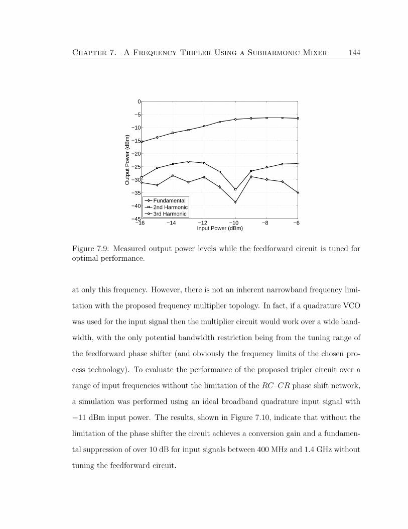
Chapter 7. A Frequency Tripler Using a Subharmonic Mixer 144
−16 −14 −12 −10 −8 −6−45
−40
−35
−30
−25
−20
−15
−10
−5
0
Input Power (dBm)
Out
put P
ower
(dB
m)
Fundamental2nd Harmonic3rd Harmonic
Figure 7.9: Measured output power levels while the feedforward circuit is tuned foroptimal performance.
at only this frequency. However, there is not an inherent narrowband frequency limi-
tation with the proposed frequency multiplier topology. In fact, if a quadrature VCO
was used for the input signal then the multiplier circuit would work over a wide band-
width, with the only potential bandwidth restriction being from the tuning range of
the feedforward phase shifter (and obviously the frequency limits of the chosen pro-
cess technology). To evaluate the performance of the proposed tripler circuit over a
range of input frequencies without the limitation of the RC–CR phase shift network,
a simulation was performed using an ideal broadband quadrature input signal with
−11 dBm input power. The results, shown in Figure 7.10, indicate that without the
limitation of the phase shifter the circuit achieves a conversion gain and a fundamen-
tal suppression of over 10 dB for input signals between 400 MHz and 1.4 GHz without
tuning the feedforward circuit.

Chapter 7. A Frequency Tripler Using a Subharmonic Mixer 145
0.4 0.6 0.8 1 1.2 1.4 1.6−35
−30
−25
−20
−15
−10
−5
0
5
10
Input Signal Frequency (GHz)
Con
vers
ion
Gai
n (d
B)
Fundamental
Third Harmonic
Figure 7.10: Simulated broadband performance of the tripler using an ideal quadra-ture input signal with a power of −11 dBm.
The phase noise degradation of the tripler was measured using the spectrum an-
alyzer for offset frequencies between 10 kHz and 1 MHz with 4207 points with 0 dB
internal attenuation and the signal-tracking option. The raw data and averaged input
and output phase noise results are shown in Figure 7.11. From theory, the minimum
phase noise degradation (PND) in a frequency multiplier is given by,
PND = 20log(n), (7.5)
where n is the order of multiplication. For the case of a frequency tripler, the minimum
phase noise degradation is 9.54 dB relative to the input signal phase noise. For
this circuit, the difference between the input and output phase noise from an offset
of 10 kHz to 1 MHz is 9.69 dB on average, which is quite close to the theoretical
minimum.

Chapter 7. A Frequency Tripler Using a Subharmonic Mixer 146
104
105
106
−130
−120
−110
−100
−90
−80
−70
Frequency Offset (Hz)
Pha
se N
oise
(dB
c/H
z)
Tripler Output
Input
Figure 7.11: Measured input and output phase noise for the frequency tripler.
The supply voltage of the circuit was set to 2.0 V and the DC current consumed
was 34 mA, resulting in a power consumption of 68 mW. A microphotograph of the
chip is shown in Figure 7.12. The dimensions of the chip including bonding pads was
1.0 mm × 0.8 mm (0.8 mm2). A performance comparison of several recent MMIC
frequency triplers with this work is presented in Table 7.1, which shows that the
proposed tripler method has advantages in terms of conversion gain and fundamental
suppression.

Chapter 7. A Frequency Tripler Using a Subharmonic Mixer 147
Figure 7.12: Microphotograph of the frequency tripler with fundamental suppressionchip.
Ref . Technology fin Conversion Fundamental Area
(GHz) Gain (dB) Supp. (dB) (mm2)
[70] GaAs (Hybrid) 1 −5.7 62.7 ∼7000
[71] InGaAs PHEMT 12 −9.4 22.3 5.0
[72] GaAs PHEMT 15 −5.6 40 2.32
[73] CMOS 0.18 µm 8.8 −10.9 22.7 0.46
[74] CMOS 90 nm 20 – – 0.81
[75] CMOS 0.18 µm 2 −5.6 13 0.18
This Work CMOS 0.18 µm 1 3 30 0.8
Table 7.1: Comparison of several recent frequency triplers with this work

Chapter 7. A Frequency Tripler Using a Subharmonic Mixer 148
7.5 Summary
A new topology for a frequency tripler circuit has been demonstrated. This technique
uses a 2× subharmonic mixer along with a feedforward circuit and a subtraction
circuit to realize fundamental cancellation. An input signal with frequency, fin, is
converted to fin and 3fin at the output of the subharmonic mixer (2fin ± fin). A
feedforward circuit is used for the input signal at fin and is connected to a summing
junction along with the output of the subharmonic mixer. In the summing junction,
the fundamental frequency signals, fin, in both the subharmonic mixer output and the
feedforward circuit output are cancelled, ideally leaving only the third harmonic, 3fin.
Advantages of this technique include the ability to realize very high levels of funda-
mental suppression without the use of a filter (up to 30 dB was obtained in this work),
as well the ability to obtain conversion gain (up to 3 dB was shown in this work).
Since no filters or inductors are required, this circuit can be implemented entirely on
chip in a relatively small area. Furthermore, phase noise measurements show that
the degradation is very close to the theoretical minimum. While the demonstration
circuit was at S-band, this technique could be used at much higher frequencies (e.g.
millimeter-wave) where the use of frequency multiplication circuits may be required.
If the proposed frequency tripler topology was implemented at a higher frequency it
may be possible to use a passive feedforward phase shifter and/or a passive subtractor
circuit on-chip, which would reduce the power consumption of the circuit.

Chapter 8
A Frequency Divider Using a
Subharmonic Mixer
8.1 Introduction
Similar to the odd-order frequency multiplier discussed in Chapter 7, odd-order high-
frequency analog frequency dividers are also much less common than even-order di-
viders (most commonly divide-by-2 or divide-by-4). Odd-order dividers can poten-
tially increase the flexibility and number of design options in a transceiver as well as
possibly reduce circuit complexity. In this chapter, a divide-by-3 frequency divider is
proposed that uses a subharmonic mixer to divide a 5.4 GHz input signal to 1.8 GHz
in CMOS 0.13 µm technology [11].
149

Chapter 8. A Frequency Divider Using a Subharmonic Mixer 150
8.2 Concept of the Frequency Divider
The concept of the proposed divide-by-three frequency divider is based on the re-
generative divider first introduced by Miller [79]. That circuit is commonly used to
implement a divide-by-two circuit using a mixer, a low-pass filter and possibly an am-
plifier. The block diagram of the traditional regenerative divider is shown in Figure
8.1.
As discussed in Chapter 2, in its steady-state this circuit has two potential mixer
outputs, 12fin and 3
2fin. A low-pass filter is then used to suppress the 3
2fin signal, which
leaves the 12fin for the feedback to the fundamental mixer as well as the output. By
using a 2× subharmonic mixer instead of a fundamental mixer it is possible to obtain
a frequency division by three. Shown in Figure 8.2 is the block diagram of the divide-
by-three circuit proposed in this thesis. The most significant change of this circuit
compared to the traditional regenerative divider shown in Figure 8.1 is the use of a
2× subharmonic mixer in place of the fundamental mixer. If the two inputs to the
subharmonic mixer are fin and fout, as shown in Figure 8.2 then at the output of the
Figure 8.1: Traditional Miller regenerative frequency divider.

Chapter 8. A Frequency Divider Using a Subharmonic Mixer 151
Figure 8.2: Block diagram of the proposed divide-by-three frequency divider.
mixer are two frequencies,
fin + 2fout (8.1)
and
fin − 2fout. (8.2)
The down-converted term in 8.2 is amplified by the tuned amplifier while the upcon-
verted term is attenuated, leaving (ideally) only the down-converted component at
the output. Therefore,
fin − 2fout = fout (8.3)
which shows the desired output,
fout =1
3fin. (8.4)
As mentioned above, the low-pass filter in Figure 8.1 has been changed to an
amplifier that is tuned to the 13fin frequency to ensure that the 5
3fin frequency has
significantly lower power at the output (and in the feedback path to the subharmonic
mixer). The use of this amplifier can improve the output power at 13fin, but also

Chapter 8. A Frequency Divider Using a Subharmonic Mixer 152
ensures that there is sufficient gain around the loop to ensure start-up of the circuit.
This tuned amplifier, however, will limit the tuning range of the frequency divider.
8.3 Circuit Design
The divide-by-three circuit is based on a single-balanced version of the 2× subhar-
monic mixer demonstrated in Chapter 3, as shown in Figure 8.3. This circuit, which is
essentially half of the 2× subharmonic mixer discussed in previous chapters, requires
only a differential LO input as opposed to the quadrature LO input required for the
double-balanced subharmonic mixer. Transistors M1 and M2 produce the doubled
Figure 8.3: Single-balanced 2× subharmonic mixer circuit.

Chapter 8. A Frequency Divider Using a Subharmonic Mixer 153
frequency, which is then mixed with the RF input to produce an output at the drains
of the RF transistors with frequency fRF ± 2fLO.
In addition to the subharmonic mixer, Figure 8.2 also shows a tuned amplifier.
To implement this amplifier, a differential pair was used with L–C loads, as shown
in Figure 8.4. The output of the subharmonic mixer will be used as input to the
differential amplifier and the output of the tuned amplifier will be fed to the gates of
the LO transistors shown in Figure 8.3.
The simplified schematic for the entire circuit is shown in Figure 8.5 (biasing not
shown). It consists of the single-balanced subharmonic mixer shown in Figure 8.3
along with the tuned amplifier in Figure 8.4 and output buffers to drive the 50 Ω load
from either the measurement equipment or the input impedance of the next stage in
the circuit.
Figure 8.4: Tuned differential amplifier circuit.

Chapter 8. A Frequency Divider Using a Subharmonic Mixer 154
Figure 8.5: Simplified schematic of the proposed frequency divider (biasing notshown).

Chapter 8. A Frequency Divider Using a Subharmonic Mixer 155
An inductor is used above the LO transistors as described in Chapter 4 in order
to increase the conversion gain of the subharmonic mixer. DC blocking capacitors are
used between the mixer output and the amplifier input and also between the output
of the amplifier and the LO transistors in order for optimal bias points to be used.
The bias point for the LO frequency doubling transistors is somewhat sensitive and
simulations showed that the optimal point is at VSS + Vt where VSS is the negative
supply voltage and Vt is the FET threshold voltage. Assuming ideal FETs that do
not conduct any current when the gate-source voltage is less than threshold voltage
the selection of this bias voltage will produce an absolute value signal (see Chapters
3 and 4 for detailed subharmonic mixer analysis). The current source shown for the
tuned differential amplifier is implemented using a standard current mirror.
8.4 Measurement Results
To evaluate the performance of the proposed divide-by-3 frequency divider, mea-
surements were performed using a probe station with differential coplanar waveguide
probes. The supply voltages were set to 1.5 V and −0.8 V for VDD and VSS, respec-
tively, and differential input and output signals were used, as shown in Figure 8.5. An
Agilent E4446A PSA Series spectrum analyzer was used with the following settings:
start frequency: 1.0 GHz, stop frequency: 6.0 GHz, RBW: 3 MHz, VBW: 3 MHz,
sweep time: 8.36 ms, 601 points, internal attenuation: 10 dB. With an input power of
−7 dBm at 5.4 GHz, the output spectrum is shown in Figure 8.6. The output spec-
tral component at 1.8 GHz (13fin) is clearly the strongest at approximately −7 dBm,
which is a conversion gain of 0 dB. The fundamental signal power at the output is
−37 dBm and therefore the fundamental suppression is 30 dB. All other harmonics

Chapter 8. A Frequency Divider Using a Subharmonic Mixer 156
1 2 3 4 5 6−80
−70
−60
−50
−40
−30
−20
−10
0
Frequency (GHz)
Out
put P
ower
(dB
m)
fin/3
fin
Figure 8.6: Measured frequency divider output spectrum with a −7 dBm input at5.4 GHz.
at the output are suppressed by at least 35 dB.
To evaluate the performance of the circuit with various input frequencies, a con-
stant input power of −7 dBm was used and the output spectrum was observed. As
discussed previously, the bandwidth of the circuit is limited by the LC tank shown
in Figure 8.5 and outside this input frequency range no output at the divide-by-three
frequency will be obtained. The measured bandwidth for a −7 dBm input power
is shown in Figure 8.7. With an input power of −7 dBm the circuit operates from
5.2 GHz to 5.5 GHz with varying levels of output power at the desired divide-by-3
spectral component. The conversion gain of the divide-by-three frequency divider has
a minimum of −1.1 dB at 5.5 GHz and a maximum of 0 dB at a 5.35 GHz input
frequency. This increased output power can be attributed to the peak tank Q-factor

Chapter 8. A Frequency Divider Using a Subharmonic Mixer 157
5.2 5.25 5.3 5.35 5.4 5.45 5.5−2
−1.5
−1
−0.5
0
0.5
1
Input Frequency (GHz)
Con
vers
ion
Gai
n (d
B)
Figure 8.7: Measured frequency divider conversion gain for various input frequencies(−7 dBm input power).
at 5.35 GHz. Since this is a regenerative topology, the output power at the divide-by-
3 frequency is relatively constant and does not increase proportionally to the input
signal power.
The initial power of the 13fin signal at the output of the subharmonic mixer is a
function of both the power of the input signal as well as the power of the feedback
signal at the other subharmonic mixer input port. Since regenerative dividers require
that the gain around the loop be greater than unity, it follows that the circuit will cease
operation at some point as the input power is decreased. Similarly, the bandwidth
of the divider will increase as the input power increases since the 13fin signal at
the subharmonic mixer output will be stronger and will compensate for the lower
amplifier gain away from the centre frequency of the amplifier. Figure 8.8 shows

Chapter 8. A Frequency Divider Using a Subharmonic Mixer 158
−16 −14 −12 −10 −8 −6 −4 −2 0 20
50
100
150
200
250
300
350
400
450
500
Input Signal Power (dBm)
Ban
dwid
th (
MH
z)
Figure 8.8: Measured frequency divider bandwidth for various input power levels.
the bandwidth attainable for various input power levels. In order for this circuit to
operate, the minimum input power level is −15 dBm and a maximum bandwidth of
430 MHz can be obtained for an input power of 1 dBm.
The phase noise of the input signal at 5.4 GHz was measured as well as the output
signal at 1.8 GHz. From theory, it would be expected that the divide-by-3 output
signal would have a 20log(n) phase noise improvement, where n = 3 (a phase noise
improvement of approximately 9.54 dB). At a 100 kHz offset, the input signal phase
noise at 5.4 GHz is −112.6 dBc/Hz and at the 1.8 GHz frequency divider output the
phase noise is −122.1 dBc/Hz. The difference between input and output phase noise
is 9.5 dB, which is very close to the theoretical value.
The dimensions of this integrated circuit measures 1000 µm × 1000 µm (1.0 mm2)
and a photograph of the chip is shown in Figure 8.9. The power consumption for the

Chapter 8. A Frequency Divider Using a Subharmonic Mixer 159
divider core circuit is 44 mW and for the entire circuit including the output buffers it
is 55 mW (similar to, for example, the divide-by-3 circuit in [84], which had a power
consumption of 45 mW).
Figure 8.9: Frequency divider chip photograph.
8.5 Summary
An analog frequency divider was presented in this chapter that can divide the fre-
quency of an input signal by a factor of three as opposed to the much more common
even-order division ratios. The proposed circuit uses a subharmonic mixer instead of
a fundamental mixer in the Miller regenerative divider as well as a tuned amplifier.
The circuit achieved a maximum conversion gain of 0 dB and a bandwidth of up to
430 MHz. All harmonic components at the output were more than 30 dB below the

Chapter 8. A Frequency Divider Using a Subharmonic Mixer 160
desired output signal. The layout for the circuit was compact at 1.0 mm2 and the
power consumption for the core of the divider was 44 mW.

Chapter 9
Summary and Conclusions
9.1 Summary
Subharmonic mixers have applications in superheterodyne systems as a method of
reducing the local oscillator frequency, as well as in direct-conversion architectures
where the use of a subharmonic mixer can reduce the significant problem of LO self-
mixing. Furthermore, subharmonic mixers can be used to realize new circuits that
would not be possible using only fundamental mixers.
This thesis’ investigation of subharmonic mixers began with a 2× subharmonic
mixer demonstrated in CMOS technology. This down-converting subharmonic mixer
used a modified Gilbert-cell topology with quadrature LO signals that were generated
on-chip from a single-ended LO input. The RF, LO, and IF ports all used active
baluns, which simplifies the use of this circuit in a system that uses single-ended
signals. A formula for the conversion gain of this mixer was derived and compared to
simulation results. The circuit was designed for an RF input signal at 2.1 GHz and
an LO frequency of 1.0 GHz, which produces a 100 MHz IF output. Measurement
161

Chapter 9. Summary and Conclusions 162
results show a conversion gain of approximately 8 dB, an input 1-dB compression
point of −14 dBm, and an IIP3 of −8.5 dBm. Since the on-chip baluns have active
input matching, the measured input reflection coefficients for both the RF and LO
ports are better than −10 dB at the frequencies of interest.
Building upon the 2× subharmonic mixer results described above, a Ku-band 4×
down-converting subharmonic mixer was proposed. This is the first 4× subharmonic
mixer demonstrated in CMOS technology and achieves the highest conversion gain
for any 4× subharmonic mixer regardless of circuit topology or process technology
used. A differential LO input signal is converted to an octet-phase signal on-chip and
is used to internally multiply the LO frequency by a factor of four. The input RF
signal is single-ended and is converted to differential on-chip using an active balun,
and the mixer’s differential output signal is converted back to single-ended also with
an active balun. An RF signal at 12.1 GHz was used for measurement along with a
3.0 GHz LO frequency, generating a 100 MHz IF output. Measurement results show a
conversion gain of approximately 6 dB, an input 1-dB compression point of −12 dBm,
IIP3 of −2 dBm, and very high isolations between the ports (e.g. 4LO–RF isolation
of 59 dB).
While the required LO signals for the 2× and 4× subharmonic mixers described
above were generated off-chip using a signal generator, in most cases there will be
an on-chip quadrature oscillator that eliminates the need for the RC–CR 90 phase
shifters. A suitable quadrature oscillator was designed for use with either of the
proposed subharmonic mixers using active superharmonic coupling. Two identical
differential oscillators were used with a 180 coupling circuit connected to common-
mode nodes where the second-order harmonics are predominant, which results in a

Chapter 9. Summary and Conclusions 163
quadrature relationship is established between the fundamental outputs. A frequency
of 3.0 GHz was used since it is the LO frequency required by the 4× subharmonic
mixer. The frequency could be adjusted for use with the 2× subharmonic mixer by
simply changing the inductors and capacitors in the resonators appropriately. This
circuit is the most compact in terms of layout area compared to other oscillators using
the superharmonic coupling technique. The oscillator output power was −6 dBm, the
phase noise was −116 dBc/Hz at a 1 MHz offset, and the phase error was less than
6.
A dual-band mixer/oscillator was presented that operates in either C-band or
X-band. Whereas many dual-band systems require a complete set of RF front-end
circuits for each band of operation, this circuit uses only a single mixer core and os-
cillator core to realize operation in both bands. Since both a fundamental and second
harmonic LO signal are available in the quadrature oscillator circuit described above,
either of these signals can be connected to a mixer. By using a set of complemen-
tary switches that control whether the fundamental or second harmonic LO signal
is connected to the mixer, operation in two frequency bands is possible. Measured
results show an RF frequency range from 5.0 GHz to 6.0 GHz for the fundamental
state of the mixer where the fundamental LO signal is connected to the mixer for a
constant IF output of 200 MHz. When the second-harmonic LO signal is connected
to the mixer the circuit is in its subharmonic state and operates with RF frequencies
between 9.8 GHz and 11.8 GHz for a constant 200 MHz IF output. Conversion gain
was attained over the entire operational frequency range for both states of the circuit.
A new frequency tripler circuit was demonstrated that uses the 2× subharmonic
mixer described previously. This circuit uses a single input for both the RF and

Chapter 9. Summary and Conclusions 164
LO ports of the subharmonic mixer, thus producing output signal components at
the fundamental input frequency and at three times the fundamental. A feedforward
circuit is used to cancel the fundamental at the output, ideally leaving only the third-
harmonic. A 1.0 GHz input signal was used and the circuit achieved a conversion
gain of up to 3 dB at the 3.0 GHz output and a fundamental suppression of over 30
dB without using a filter at the output.
Lastly, a frequency divider was presented that is unique in that it divides the fre-
quency of an input signal by a factor of three, whereas the vast majority of frequency
dividers divide the input signal by an even-ordered factor (usually two or four). This
circuit uses a single-balanced 2× subharmonic mixer in a Miller regenerative divider
topology. Measurement results show a maximum conversion gain of 0 dB and suppres-
sion of the input signal frequency at the output of up to 30 dB. With an input power
of −7 dBm this circuit operates with an input signal frequency between 5.2 GHz and
5.5 GHz, producing an output from 1.73 GHz to 1.83 GHz.
9.2 Review of Contributions
This thesis has contributed to the field of microwave engineering in several ways re-
garding the design and applications of CMOS subharmonic mixers. In this thesis
one of the first subharmonic mixers with measured results in CMOS technology was
presented; this was the first to use the proposed mixer topology. Furthermore, this
2× subharmonic mixer had a conversion gain and other performance metrics similar
to fundamental mixers. Since single-ended signals are often used, this subharmonic
mixer used input and output active baluns to make the conversion from single-ended

Chapter 9. Summary and Conclusions 165
inputs to differential for internal operation, and then back to single-ended for mea-
surements.
The concept of the 2× subharmonic mixer was used as a basis for a more advanced
4× subharmonic mixer that operates at Ku-band. This circuit was the first 4× sub-
harmonic mixer using CMOS technology and it achieves the highest conversion gain
for any 4× subharmonic mixer regardless of circuit topology or fabrication technology
used.
Since both the 2× and 4× subharmonic mixers require a quadrature oscillator, a
new design was shown that could be used with either of the aforementioned mixers.
This oscillator was designed to require minimal chip area, and in fact was the most
compact quadrature oscillator that could be found in the literature that uses the
superharmonic coupling technique. Furthermore, this oscillator had the lowest phase
noise for an oscillator using active superharmonic coupling.
A dual-band mixer/oscillator was presented that can operate in either the C-band
or the X-band using single mixer and oscillator core circuits. Since these two circuits
can operate in two bands, the use of duplicate circuitry for each band, as has often
been used in the past, is avoided.
Next, a frequency tripler circuit was presented that is based on the 2× subhar-
monic mixer previously discussed. This circuit is unique in several aspects. First,
there are very few frequency triplers in the literature – most frequency multipliers are
times two or times four. The addition of a tripler circuit allows for more flexibility in
the transceiver design and can potentially eliminate the need for additional oscillators.
Also, this circuit can achieve high levels of fundamental suppression without filtering
the output signal since a feedforward circuit is used to cancel the fundamental signal

Chapter 9. Summary and Conclusions 166
component at the output. The elimination of a filter at the output of the frequency
multiplier can save significant space on-chip or avoid taking the signal off-chip to be
filtered by an off-chip SAW or FBAR filter, for example.
Finally, a divide-by-three frequency divider was demonstrated that is based on
a 2× subharmonic mixer. Measurement results show that this topology can achieve
very low conversion loss or even conversion gain and high-levels of suppression of
the undesired signals at the output. There have been very few odd-order frequency
divider circuits previously demonstrated, and this work can add flexibility to circuits
and systems by removing the limitation imposed by even-ordered dividers that have
been dominant in the past.
9.3 Future Work
There are several potential directions for future work on subharmonic mixers. The 4×
subharmonic mixer topology described in this thesis becomes even more attractive as
the operational frequency is increased since it becomes more difficult to design a local
oscillator. Therefore, the 4× subharmonic mixer circuit could be implemented at a
much higher frequency, for example, 40 GHz or above. Similarly, the frequency tripler
topology could be applied at millimeter-wave frequencies where frequency multipliers
are often required.
A direct-conversion receiver could be designed around either the 2× or 4× sub-
harmonic mixers in order to determine the maximum performance that is attainable
with the use of these subharmonic mixers.
An increase in the order of subharmonic mixing could be investigated. For exam-
ple, an 8× subharmonic mixer. However, this may be challenging using the proposed

Chapter 9. Summary and Conclusions 167
topologies since it would require splitting the LO into 16 phases. Furthermore, a
study into increasing the performance of the proposed subharmonic mixers could be
undertaken. For example, a low-noise or high-linearity version of the 2× or 4× sub-
harmonic mixers could be designed to further increase the attractiveness of using
subharmonic mixers in a variety of applications.
Lastly, a modification to the dual-band mixer/oscillator could be performed to
realize a tri-band circuit that could operate as either a fundamental mixer, a 2×
subharmonic mixer, or a 4× subharmonic mixer.

References
[1] T. Lee, The Design of CMOS Radio-Frequency Integrated Circuits. Cambridge
University Press, 2002.
[2] B. Razavi, “A 60-GHz CMOS Receiver Front-End,” IEEE Journal of Solid-
State Circuits, vol. 41, pp. 17–22, January 2006.
[3] C. Cao, E. Seok, and K. O, “192 GHz Push-Push VCO in 0.13 µm CMOS,”
Electronics Letters, vol. 42, pp. 208–210, Feb. 2006.
[4] S. Lee, B. Jagannathan, S. Narasimha, A. Chou, N. Zamdmer, J. Johnson,
R. Williams, L. Wagner, J. Kim, J.-O. Plouchart, J. Pekarik, S. Springer, and
G. Freeman, “Record RF Performance of 45-nm SOI CMOS Technology,” IEEE
International Electron Devices Meeting, pp. 255–258, Dec. 2007.
[5] Y.-J. E. Chen, K.-H. Wang, T.-N. Luo, S.-Y. Bai, and D. Heo, “Investigation of
CMOS Technology for 60-GHz Applications,” IEEE SoutheastCon, pp. 92–95,
April 2005.
[6] B. Jackson and C. E. Saavedra, “A CMOS Ku-Band 4x Subharmonic Mixer,”
IEEE Journal of Solid-State Circuits, vol. 43, pp. 1351–1359, June 2008.
168

References 169
[7] B. Jackson and C. E. Saavedra, “A Frequency Tripler using a Subharmonic
Mixer and Fundamental Cancellation,” IEEE Transactions on Microwave The-
ory and Techniques. to appear May 2009.
[8] B. R. Jackson and C. E. Saavedra, “A CMOS Subharmonic Mixer with Input
and Output Active Baluns,” Microwave and Optical Technology Letters (Wiley
InterScience), vol. 48, pp. 2472–2478, December 2006.
[9] B. Jackson and C. Saavedra, “A 3 GHz CMOS Quadrature Oscillator using
Active Superharmonic Coupling,” European Microwave Conference, pp. 1109–
1112, Oct. 2007.
[10] B. Jackson and C. E. Saavedra, “A Dual-Band Mixer/Oscillator for C-Band
and X-Band Applications,” IEEE Transactions on Microwave Theory and Tech-
niques. Submitted for review January 2009.
[11] B. Jackson and C. E. Saavedra, “A Divide-By-3 Frequency Divider using a Sub-
harmonic Mixer,” 2010 IEEE Radio Frequency Integrated Circuits Symposium
(RFIC 2010). To be submitted.
[12] C. E. Saavedra, “ELEC 457 Course Notes,” 2008.
[13] E. Armstrong, “Method of Receiving High Frequency Oscillation,” U.S. Patent
1,342,885, June 8, 1920.
[14] D. Manstretta, M. Brandolini, and F. Svelto, “Second-order Intermodulation
Mechanisms in CMOS Downconverters,” IEEE Journal of Solid-State Circuits,
vol. 38, pp. 394–406, March 2003.

References 170
[15] R. Svitek and S. Raman, “DC Offsets in Direct-Conversion Receivers: Char-
acterization and Implications,” IEEE Microwave Magazine, vol. 6, pp. 76–86,
September 2005.
[16] R. G. Meyer, W. D. Mack, and J. J. E. M. Hageraats, “A 2.5-GHz BiCMOS
Transceiver for Wireless LAN’s,” IEEE Journal of Solid-State Circuits, vol. 32,
pp. 2097–2104, December 1997.
[17] B. Gilbert, “A Precise Four-Quadrant Multiplier with Subnanosecond Re-
sponse,” IEEE Journal of Solid-State Circuits, vol. 3, pp. 365–373, December
1968.
[18] C.-S. Lin, P.-S. Wu, H.-Y. Chang, and H. Wang, “A 9-50 GHz Gilbert-Cell
Down-Conversion Mixer in 0.13-µm CMOS Technology,” Microwave and Wire-
less Components Letters, IEEE, vol. 16, pp. 293–295, May 2006.
[19] M.-D. Tsai and H. Wang, “A 0.3-25 GHz Ultra-Wideband Mixer Using Com-
mercial 0.18 µm CMOS Technology,” IEEE Microwave and Wireless Component
Letters, vol. 14, pp. 522–524, November 2004.
[20] F. Ellinger, “26.5–30-GHz Resistive Mixer in 90-nm VLSI SOI CMOS Tech-
nology With High Linearity for WLAN,” Microwave Theory and Techniques,
IEEE Transactions on, vol. 53, pp. 2559–2565, Aug. 2005.
[21] M. Bao, H. Jacobsson, L. Aspemyr, G. Carchon, and X. Sun, “A 9–31-GHz
Subharmonic Passive Mixer in 90-nm CMOS Technology,” IEEE Journal of
Solid-State Circuits, vol. 41, pp. 2257–2264, October 2006.

References 171
[22] H.-C. Chen, T. Wang, S.-S. Lu, and G.-W. Huang, “A Monolithic 5.9-
GHz CMOS I/Q Direct-Down Converter Utilizing a Quadrature Coupler and
Transformer-Coupled Subharmonic Mixers,” IEEE Microwave and Wireless
Components Letters, vol. 16, pp. 197–199, April 2006.
[23] J.-H. Tsai, H.-Y. Yang, T.-W. Huang, and H. Wang, “A 30–100 GHz Wide-
band Sub-Harmonic Active Mixer in 90 nm CMOS Technology,” Microwave
and Wireless Components Letters, IEEE, vol. 18, pp. 554–556, Aug. 2008.
[24] H. Feng, Q. W. X. Guan, R. Zhan, A. Wang, and L. W. Yang, “A 5 GHz Sub-
Harmonic Direct Down-Conversion Mixer for Dual-Band System in 0.35 µm
SiGe BiCMOS,” in IEEE International Symposium on Circuits and Systems,
vol. 5, (Kobe Japan), pp. 4807–4810, May 2005.
[25] H.-M. Hsu and T.-H. Lee, “A Zero-IF Sub-Harmonic Mixer with High LO-RF
Isolation using 0.18 µm CMOS Technology,” in IEEE European Microwave In-
tegrated Circuits Conference, (Manchester, UK), pp. 336–339, September 2006.
[26] M.-F. Huang, S.-Y. Lee, and C. J. Kuo, “A 5.25 GHz CMOS Even Harmonic
Mixer with an Enhancing Inductance,” in IEEE International Symposium on
Circuits and Systems, vol. 3, (Kobe Japan), pp. 2116–2119, May 2005.
[27] J.-J. Hung, T. M. Hancock, and G. M. Rebeiz, “A 77 GHz SiGe Sub-Harmonic
Balanced Mixer,” IEEE Journal of Solid-State Circuits, vol. 40, pp. 2167–2173,
November 2005.

References 172
[28] R. M. Kodkani, L. E. Larson, and E. Lawrence, “A 24-GHz CMOS Direct-
Conversion Sub-Harmonic Downconverter,” in IEEE Radio Frequency Inte-
grated Circuits (RFIC) Symposium, (Honolulu, Hawaii, USA), pp. 485–488,
June 2007.
[29] K.-J. Koh, M.-Y. Park, C.-S. Kim, and H.-K. Yu, “Subharmonically Pumped
CMOS Frequency Conversion (Up and Down) Circuits for 2-GHz WCDMA
Direct-Conversion Transceiver,” IEEE Journal of Solid-State Circuits, vol. 39,
pp. 871–884, June 2004.
[30] M.-Y. Lee, C.-Y. Jeong, C. Yoo, Y.-H. Kim, J.-H. Hwang, and J.-S. Park,
“Fully-Integrated CMOS Direct-Conversion Receiver for 5GHz Wireless LAN,”
in IEEE Topical Meeting on Silicon Monolithic Integrated Circuits in RF Sys-
tems, (Long Beach, CA, USA), pp. 201–204, January 2007.
[31] R. Svitek and S. Raman, “5–6 GHz SiGe Active I/Q Subharmonic Mixers with
Power Supply Noise Effect Characterization,” IEEE Microwave and Wireless
Components Letters, vol. 14, pp. 319–321, July 2004.
[32] P. Upadhyaya, M. Rajashekharaiah, Y. Zhang, D. Heo, and Y.-J. Chen, “A
High IIP2 Doubly Balanced Sub-Harmonic Mixer in 0.25-µm CMOS for 5-GHz
ISM Band Direct Conversion Receiver,” in IEEE Radio Frequency Integrated
Circuits Symposium, (Long Beach, California, USA), pp. 175–178, June 2005.
[33] T.-H. Wu, S.-C. Tseng, C.-C. Meng, and G.-W. Huang, “GaInP/GaAs HBT
Sub-Harmonic Gilbert Mixers Using Stacked-LO and Leveled-LO Topologies,”
IEEE Transactions on Microwave Theory and Techniques, vol. 55, pp. 880–889,
May 2007.

References 173
[34] T.-Y. Yang and H.-K. Chiou, “A 28 GHz Sub-Harmonic Mixer using LO Dou-
bler in 0.18-µm CMOS Technology,” in IEEE Radio Frequency Integrated Cir-
cuits (RFIC) Symposium, (San Francisco, California, USA), June 2006.
[35] L. Sheng, J. C. Jensen, and L. E. Larson, “A Wide-Bandwidth Si/SiGe HBT Di-
rect Conversion Sub-Harmonic Mixer/Downconverter,” IEEE Journal of Solid-
State Circuits, vol. 35, pp. 1329–1337, September 2000.
[36] K. Nimmagadda and G. Rebeiz, “A 1.9 GHz Double-Balanced Subharmonic
Mixer for Direct Conversion Receivers,” IEEE Radio Frequency Integrated Cir-
cuits (RFIC) Symposium, pp. 253–256, 2001.
[37] B. G. Perumana, C.-H. Lee, J. Laskar, and S. Chakraborty, “A Subharmonic
CMOS Mixer Based on Threshold Voltage Modulation,” IEEE MTT-S Inter-
national Microwave Symposium Digest, pp. 33–36, June 2005.
[38] M. W. Chapman and S. Raman, “A 60-GHz Uniplanar MMIC 4x Subharmonic
Mixer,” IEEE Transactions on Microwave Theory and Techniques, vol. 50,
pp. 2580–2588, November 2002.
[39] K. Kanaya, K. Kawakami, T. Hisaka, T. Ishikawa, and S. Sakamoto, “A 94
GHz High Performance Quadruple Subharmonic Mixer MMIC,” IEEE MTT-S
International Microwave Symposium Digest, vol. 2, pp. 1249–1252, June 2002.
[40] A. Madjar and M. Musia, “Design and Performance of a x4 Millimeter Wave
Subharmonic Mixer,” in IEEE European Microwave Conference, (Madrid,
Spain), pp. 246–247, October 1993.

References 174
[41] S. Sarkar, D. Yeh, S. Pinel, and J. Laskar, “Wideband Direct Conversion Hybrid
LCP Millimeter-Wave 4× Subharmonic Mixer for Gigabit Wireless Module,” in
IEEE European Microwave Conference, (Paris, France), October 2005.
[42] W.-Y. Uhm, W.-S. Sul, H.-J. Han, S.-C. Kim, H.-S. Lee, D. An, S.-D. Kim,
D.-H. Shin, H.-M. Park, and J.-K. Rhee, “A High Performance V-band Mono-
lithic Quadruple Sub-Harmonic Mixer,” IEEE MTT-S International Microwave
Symposium Digest, vol. 2, pp. 1319–1322, June 2003.
[43] D. An, S. C. Kim, W. S. Sul, H. J. Han, H. S. Lee, W. Y. Uhm, H. M. Park,
S. D. Kim, D. H. Shin, and J. K. Rhee, “High Conversion Gain V-band Quadru-
ple Subharmonic Mixer using Cascode Structure,” IEEE MTT-S International
Microwave Symposium Digest, vol. 2, pp. 911–914, June 2003.
[44] A. A. Abidi, “Direct-Conversion Radio Transceivers for Digital Communica-
tions,” IEEE Journal of Solid-State Circuits, vol. 30, pp. 1399–1410, December
1995.
[45] A. Niknejad and R. Meyer, “Analysis, Design, and Optimization of Spiral In-
ductors and Transformers for Si RF ICs,” IEEE Journal of Solid-State Circuits,
vol. 33, pp. 1470–1481, Oct 1998.
[46] C. Yue and S. Wong, “On-Chip Spiral Inductors with Patterned Ground Shields
for Si-Based RF ICs,” IEEE Journal of Solid-State Circuits, vol. 33, pp. 743–
752, May 1998.
[47] A. Sedra and K. Smith, Microelectronic Circuits. Oxford University Press, 1998.

References 175
[48] M.-D. Tsai, Y.-H. Cho, and H. Wang, “A 5-GHz Low Phase Noise Differential
Colpitts CMOS VCO,” Microwave and Wireless Components Letters, IEEE,
vol. 15, pp. 327–329, May 2005.
[49] Z. Liu, E. Skafidas, and R. Evans, “A 60 GHz VCO with 6 GHz Tuning Range
in 130 nm Bulk CMOS,” U.S., vol. 1, pp. 209–211, April 2008.
[50] A. Hajimiri and T. Lee, “Design Issues in CMOS Differential LC Oscillators,”
IEEE Journal of Solid-State Circuits, vol. 34, pp. 717–724, May 1999.
[51] N. Pletcher, Micro Power Radio Frequency Oscillator Design. M.Sc. Thesis,
University of California, Berkeley, 2004.
[52] L. Jia, J.-G. Ma, K. Yeo, and M. Do, “9.3–10.4-GHz-Band Cross-Coupled Com-
plementary Oscillator With Low Phase-Noise Performance,” IEEE Transactions
on Microwave Theory and Techniques, vol. 52, pp. 1273–1278, April 2004.
[53] J. Craninckx and M. S. J. Steyaert, “A Fully Integrated CMOS DCS-1800
Frequency Synthesizer,” IEEE Journal of Solid-State Circuits, vol. 33, pp. 2054–
2065, December 1998.
[54] J. P. Maligeorgos and J. R. Long, “A Low-Voltage 5.1-5.8 GHz Image-Reject
Receiver with Wide Dynamic Range,” IEEE Journal of Solid-State Circuits,
vol. 35, pp. 1917–1926, December 2000.
[55] A. Rofougaran, G. Chang, J. Rael, J.-C. Chang, M. Rofougaran, P. Chang,
M. Djafari, M.-K. Ku, E. Roth, A. Abidi, and H. Samueli, “A Single-Chip 900-
MHz Spread-Spectrum Wireless Transceiver in 1-µm CMOS. I. Architecture and

References 176
Transmitter Design,” IEEE Journal of Solid-State Circuits, vol. 33, pp. 515–
534, Apr 1998.
[56] C. Meng, Y. Chang, and S. Tseng, “4.9-GHz Low-Phase-Noise Transformer-
Based Superharmonic-Coupled GaInP/GaAs HBT QVCO,” IEEE Microwave
and Wireless Components Letters, vol. 16, pp. 339–341, June 2006.
[57] J. Cabanillas, L. Dussopt, J. Lopez-Villegas, and G. Rebeiz, “A 900 MHz Low
Phase Noise CMOS Quadrature Oscillator,” IEEE Radio Frequency Integrated
Circuits (RFIC) Symposium, pp. 63–66, 2002.
[58] S. Gierkink, S. Levantino, R. Frye, C. Samori, and V. Boccuzzi, “A Low-Phase-
Noise 5-GHz CMOS Quadrature VCO using Superharmonic Coupling,” IEEE
Journal of Solid-State Circuits, vol. 38, pp. 1148–1154, July 2003.
[59] T. Hancock and G. Rebeiz, “A Novel Superharmonic Coupling Topology for
Quadrature Oscillator Design at 6 GHz,” IEEE Radio Frequency Integrated
Circuits (RFIC) Symposium, pp. 285–288, June 2004.
[60] F. Ellinger and H. Jackel, “Ultracompact SOI CMOS Frequency Doubler for
Low Power Applications at 26.5–28.5 GHz,” IEEE Microwave Wireless Com-
ponent Letters, vol. 14, pp. 53–55, February 2004.
[61] J. Wong and H. Luong, “A 1.5-V 4-GHz Dynamic-Loading Regenerative Fre-
quency Doubler in a 0.35 µm CMOS Process,” IEEE Trans. on Circuits and
Systems II: Analog and Digital Signal Processing, vol. 50, pp. 450–455, August
2003.

References 177
[62] M. Yang, S. Oh, and S. Lee, “Low Power Fully Differential Frequency Doubler,”
IEE Electronics Letters, vol. 39, pp. 1388–1389, September 2003.
[63] Q. Xiao, J. Hesler, T. Crowe, R. Weikle, Y. Duan, and B. Deaver, “High-
Efficiency Heterostructure-Barrier-Varactor Frequency Triplers using AIN Sub-
strates,” in IEEE MTT-S Int. Microwave Symp. Digest, (Long Beach, USA),
pp. 443–446, June 2005.
[64] R. Meola, J. Freyer, and M. Claassen, “Improved Frequency Tripler with In-
tegrated Single-Barrier Varactor,” IEE Electronics Lett., vol. 36, pp. 803–804,
April 2000.
[65] J. R. Jones, W. L. Bishop, S. H. Jones, and G. B. Tait, “Planar Multibar-
rier 80/240-GHz Heterostructure Barrier Varactor Triplers,” IEEE Trans. Mi-
crowave Theory and Tech., vol. 45, pp. 512–518, April 1997.
[66] S.-S. Liao, H.-K. Chen, P.-T. Sun, C.-Y. Lai, H.-Y. Liao, and Y.-C. Chang,
“Novel Design for Small-Size Coplanar Waveguide Frequency Tripler,” IEEE
Microwave Wireless Component Lett., vol. 13, pp. 529–531, December 2003.
[67] Y. Campos-Roca, L. Verweyen, M. Fernandez-Barciela, E. Sanchez, M. C.
Curras-Francos, W. Bronner, A. Hulsmann, and M. Schlechtweg, “An Opti-
mized 25.5–76.5 GHz PHEMT-Based Coplanar Frequency Tripler,” IEEE Mi-
crowave Guided Wave Lett., vol. 10, pp. 242–244, June 2000.
[68] A. Boudiaf, D. Bachelet, and C. Rumelhard, “38 GHz MMIC PHEMT-Based
Tripler with Low Phase-Noise Properties,” in IEEE MTT-S Int. Microwave
Symp. Digest, vol. 1, (Boston, USA), pp. 509–512, June 2000.

References 178
[69] B. Bunz and G. Kompa, “Broadband HEMT-Based Frequency Tripler for use in
Active Multi-Harmonic Load-Pull System,” in 34th European Microwave Con-
ference, (Amsterdam, The Netherlands), pp. 193–196, October 2004.
[70] S. Seo, Y. Jeong, J. Lim, B. Gray, and J. Kenney, “A Novel Design of Frequency
Tripler Using Composite Right/Left Handed Transmission Line,” Microwave
Symposium, 2007. IEEE/MTT-S International, pp. 2185–2188, June 2007.
[71] J.-C. Chiu, C.-P. Chang, M.-P. Houng, and Y.-H. Wang, “A 12–36GHz PHEMT
MMIC Balanced Frequency Tripler,” Microwave and Wireless Components Let-
ters, IEEE, vol. 16, pp. 19–21, Jan. 2006.
[72] H. Fudem and E. Niehenke, “Novel Millimeter Wave Active MMIC Triplers,”
Microwave Symposium Digest, 1998 IEEE MTT-S International, vol. 2,
pp. 387–390, Jun 1998.
[73] M.-C. Chen and C.-Y. Wu, “Design and Analysis of CMOS Subharmonic
Injection-Locked Frequency Triplers,” Microwave Theory and Techniques, IEEE
Transactions on, vol. 56, pp. 1869–1878, Aug. 2008.
[74] W. Chan, J. Long, and J. Pekarik, “A 56-to-65GHz Injection-Locked Frequency
Tripler with Quadrature Outputs in 90nm CMOS,” Solid-State Circuits Con-
ference, 2008. ISSCC 2008. Digest of Technical Papers. IEEE International,
pp. 480–629, Feb. 2008.
[75] Y. Zheng and C. E. Saavedra, “A Broadband CMOS Frequency Tripler using a
Third-Harmonic Enhanced Technique,” IEEE Journal of Solid-State Circuits,
vol. 42, pp. 2197–2203, October 2007.

References 179
[76] F. Cheng, C. Chen, and O. Choy, “A 1.0 µm CMOS All Digital Clock Multi-
plier,” in IEEE 40th Midwest Symposium on Circuits and Systems, pp. 460–462,
August 1997.
[77] S. Henzler and S. Koeppe, “Design and Application of Power Optimized High-
Speed CMOS Frequency Dividers,” Very Large Scale Integration (VLSI) Sys-
tems, IEEE Transactions on, vol. 16, pp. 1513–1520, November 2008.
[78] T. S. Aytur and B. Razavi, “A 2 GHz, 6 mW BiCMOS Frequency Synthesizer,”
IEEE Journal of Solid-State Circuits, vol. 30, pp. 1457–1462, December 1995.
[79] R. L. Miller, “Fractional-Frequency Generators Utilizing Regenerative Modula-
tion,” Proc. IRE, vol. 27, pp. 446–456, July 1939.
[80] J. Lee and B. Razavi, “A 40-GHz Frequency Divider in 0.18-µm CMOS Tech-
nology,” IEEE Journal of Solid-State Circuits, vol. 39, pp. 594–601, April 2004.
[81] L. Landen, C. Fager, and H. Zirath, “Regenerative GaAs MMIC Frequency
Dividers for 28 and 14 GHz,” European Microwave Conference, 2000. 30th,
pp. 1–3, Oct. 2000.
[82] H. Rategh and T. Lee, “Superharmonic Injection-Locked Frequency Dividers,”
IEEE Journal of Solid-State Circuits, vol. 34, pp. 813–821, Jun 1999.
[83] J.-C. Chien, C.-S. Lin, L.-H. Lu, H. Wang, J. Yeh, C.-Y. Lee, and J. Chern,
“A Harmonic Injection-Locked Frequency Divider in 0.18-µm SiGe BiCMOS,”
Microwave and Wireless Components Letters, IEEE, vol. 16, pp. 561–563, Oct.
2006.
References 180
[84] H. Wu and L. Zhang, “A 16-to-18 GHz 0.18-µm Epi-CMOS Divide-by-3
Injection-Locked Frequency Divider,” Solid-State Circuits Conference, 2006.
ISSCC 2006. Digest of Technical Papers. IEEE International, pp. 2482–2491,
6-9, 2006.
[85] M. Acar, D. Leenaerts, and B. Nauta, “A Wide-Band CMOS Injection-Locked
Frequency Divider,” IEEE Radio Frequency Integrated Circuits (RFIC) Sym-
posium, pp. 211–214, June 2004.
[86] Z. Zhaofeng, L. Tsui, C. Zhiheng, and J. Lau, “A CMOS Self-Mixing-Free Front-
End for Direct Conversion Applications,” in IEEE International Symposium on
Circuits and Systems, (Sydney, Australia), pp. 386–389, May 2001.
[87] P. Upadhyaya, M. Rajashekharaiah, Y. Zhang, D. Heo, and Y.-J. Chen, “A 5
GHz Novel 0.18 µm Inductor-less CMOS Sub-harmonic Mixer,” in IEEE Fourth
International Symposium on Information Processing in Sensor Networks, (Los
Angeles, California, USA), pp. 71–74, April 2005.
[88] V. Krizhanovskii and S.-G. Lee, “0.18 µm CMOS Sub-harmonic Mixer for 2.4
GHz IEEE 802.15.4 Transceiver,” in IEEE 14th International Crimean Confer-
ence on Microwave and Telecommunication Technology, (Sevastopol, Crimea,
Ukraine), pp. 141–142, September 2004.
[89] P. Upadhyaya, M. Rajashekharaiah, and D. Heo, “A 5.6 GHz CMOS Dou-
bly Balanced Sub-Harmonic Mixer for Direct Conversion Zero IF Receiver,”
in IEEE Workshop on Microelectronics and Electron Devices, (Boise, Idaho,
USA), pp. 129–130, April 2004.

References 181
[90] M. Goldfarb, J. B. Cole, and A. Platzker, “A Novel MMIC Biphase Modulator
with Variable Gain using Enhancement-Mode FETs Suitable for 3 V Wireless
Applications,” in IEEE Microwave and Millimeter-Wave Monolithic Circuits
Symposium, pp. 99–102, 1994.
[91] L. M. Devlin, B. J. Buck, J. C. Clifton, A. W. Dearn, , and A. P. Long, “A
2.4 GHz Single Chip Transceiver,” in IEEE Microwave and Millimeter-Wave
Monolithic Circuits Symposium, pp. 23–26, 1993.
[92] M. Kawashima, T. Nakagawa, and K. Araki, “A Novel Broadband Active
Balun,” in IEEE 33rd European Microwave Conference, (Munich, Germany),
pp. 495–498, October 2003.
[93] M. Rajashekharaiah and E. Chen, “A New 0.25 µm CMOS On-Chip Active
Balun with Gain Controllability for 5 GHz DCR,” in IEEE 7th International
Conference on Solid-State and Integrated Circuits Technology, (Beijing, China),
pp. 1295–1298, October 2004.
[94] H. Darabi and A. A. Abidi, “Noise in RF-CMOS Mixers: A Simple Physical
Model,” IEEE Journal of Solid-State Circuits, vol. 35, pp. 15–25, January 2000.
[95] P. Andreani and X. Wang, “On the Phase-Noise and Phase-Error Performances
of Multiphase LC CMOS VCOs,” IEEE Journal of Solid-State Circuits, vol. 39,
pp. 1883–1893, November 2004.
[96] Y.-S. Hwang, S. sun Yoo, and H.-J. Yoo, “A 2 GHz and 5 GHz Dual-Band Direct
Conversion RF Frontend for Multi-Standard Applications,” IEEE International
SOC Conference, pp. 189–192, Sept. 2005.

References 182
[97] T. Abdelrheem, H. Elhak, and K. Sharaf, “A Concurrent Dual-Band Mixer for
900 MHz/1.8 GHz RF Front-Ends,” Proceedings of the 46th IEEE International
Midwest Symposium on Circuits and Systems, 2003, vol. 3, pp. 1291–1294 Vol.
3, Dec. 2003.
[98] W. Kim, J. Yu, H. Shin, S.-G. Yang, W. Choo, and B.-H. Park, “A Dual-
Band RF Front-End of Direct Conversion Receiver for Wireless CDMA Cellular
Phones with GPS Capability,” IEEE Transactions on Microwave Theory and
Techniques, vol. 54, pp. 2098–2105, May 2006.
[99] M. Arasu, Y. Zheng, and W. G. Yeoh, “A 3 to 9-GHz Dual-band Up-Converter
for a DS-UWB Transmitter in 0.18-µm CMOS,” IEEE Radio Frequency Inte-
grated Circuits (RFIC) Symposium, pp. 497–500, June 2007.
[100] P. de Paco, R. Villarino, G. Junkin, O. Menendez, E. Corrales, and J. Parron,
“Dual-Band Mixer Using Composite Right/Left-Handed Transmission Lines,”
IEEE Microwave and Wireless Components Letters, vol. 17, pp. 607–609, Aug.
2007.
[101] M. Schmatz, C. Biber, and W. Baumberger, “Conversion Gain Enhancement
Technique for Ultra Low Power Gilbert-Cell Down Mixers,” in IEEE Gallium
Arsenide Integrated Circuit (GaAs IC) Symposium, (San Diego, CA, USA),
pp. 245–248, October 1995.