stress aware active area sizing, gate sizing and repeater ... · stress aware active area sizing,...
TRANSCRIPT

Stress Aware Active Area Sizing, Gate Sizing and Repeater Insertion
Ashutosh Chakraborty David Z. [email protected] [email protected]
ECE Department, University of Texas at Austin
Outline
Intro. to source/drain (S/D) SiGe technology
Active Area (AA) aware Delay Model
AA aware Optimal Repeater Insertion (ORI)
Concurrent AA and Gate Sizing
Conclusions

Outline
Intro. to source/drain (S/D) SiGe technology
SiGe Active Area (AA) aware Delay Model
AA aware Optimal Repeater Insertion (ORI)
Concurrent AA and Gate Sizing
Conclusions

Stress/Strain Basics
Squeezing lattice produces compressive stress
Pulling lattice apart produces tensile stress
In direction of charge carrier flow,› Compressive stress improves PMOS performance› Tensile stress improves NMOS performance› Larger stress means more performance benefit.
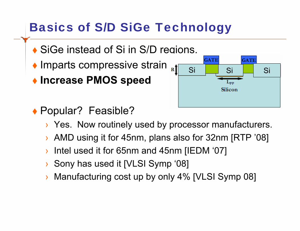
Basics of S/D SiGe Technology
SiGe instead of Si in S/D regions.Imparts compressive strainIncrease PMOS speed
Popular? Feasible?› Yes. Now routinely used by processor manufacturers.› AMD using it for 45nm, plans also for 32nm [RTP ’08]› Intel used it for 65nm and 45nm [IEDM ‘07]› Sony has used it [VLSI Symp ‘08]› Manufacturing cost up by only 4% [VLSI Symp 08]
Si Si Si

S/D SiGe Aware active area (AA) sizing
Factor affecting this mobility enhancement:› Active area dimension (Lpp)› Concentration of Ge› Recess depth R
Layout designer can control active area (AA) size› Traditionally, trained to minimize it› However, with S/D SiGe, increasing AA helps!
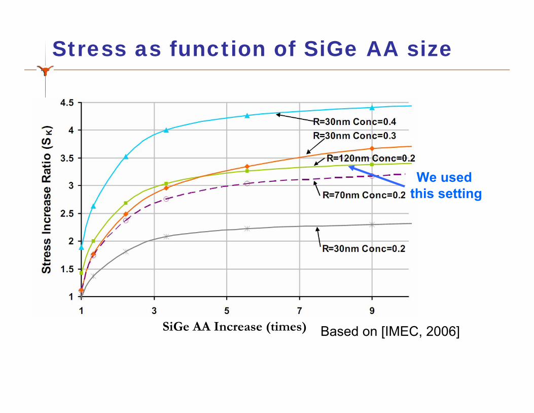
Stress as function of SiGe AA size
Based on [IMEC, 2006]SiGe AA Increase (times)
We used this setting

Previous Works
Modeling SiGe AA increase impact› Eneman, VLSI Symp ’05› Simoen, Trans Elect. Dev. ’08› Applied Materials ’07 report
SiGe AA aware layout optimization› Chakraborty, DATE 08› Joshi, ISPD 08› Joshi, DAC 08
SiGe AA aware physical synthesis› None existing.› This work targets this void.
RTL
PhysicalSynthesis
Layout
FabricationFabrication
Layout
PhysicalSynthesis
Motivational Example
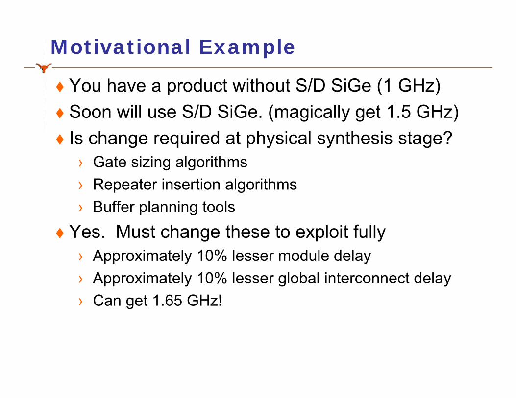
You have a product without S/D SiGe (1 GHz)Soon will use S/D SiGe. (magically get 1.5 GHz)Is change required at physical synthesis stage?
› Gate sizing algorithms› Repeater insertion algorithms› Buffer planning tools
Yes. Must change these to exploit fully› Approximately 10% lesser module delay› Approximately 10% lesser global interconnect delay› Can get 1.65 GHz!

Outline
Intro. to source/drain (S/D) SiGe technology
SiGe Active Area (AA) aware Delay Model
AA aware Optimal Repeater Insertion (ORI)
Concurrent AA and Gate Sizing
Conclusions

Cell Delay Model Derivation
Analyze cell layout to obtain RC switch model› Consider AA aware PMOS resistance values› Consider increased self-loading capacitances
Compute new fall and rise timeAverage fall and rise delay to get cell delay
S C DG W
L LppLpp
S C DG W
L L’ppL’pp

PMOS Resistance Decrease
Stress Mobility (µ) RON (ON resistance)
By curve fitting
Relates PMOS RON decrease to SiGe AA increase. Value of “A”depends on Ge conc and recess depth. For our settings, A = 3.4.

Example [NAND Gate]
D(K) = RC ((F+1)(K+0.5*h+1) + 0.5)
Characteristic Delay Equation
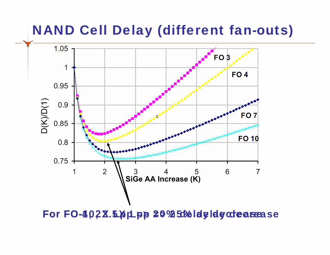
For FO-4, 2X Lpp => 20% delay decrease
NAND Cell Delay (different fan-outs)
For FO-10, 2.5X Lpp => 25% delay decrease
D(K
)/D(1
)
SiGe AA Increase (K)

Delay Decrease for other Gates
3 input NOR
2 input NOR
3 input NAND
2 input NAND
INV
Gate
-16.1%RC ((F+1)(3K+0.5*h+1) + 3FK)
-16.4%RC ((F+1)(2K+0.5*h+0.5) + FK)
-16.2%RC ((F+1)(2K+0.5*h+1.5) + 1.5)
-21.9%RC ((F+1)(K+0.5*h+1) + 0.5)
-17.9%RC (F+1)(K+0.5*h+0.5)
ΔD @ FO4Characteristic Delay Equation
Outline
Intro. to source/drain (S/D) SiGe technology
Cell Delay Model Derivation
AA aware Optimal Repeater Insertion (ORI)
Concurrent AA and Gate Sizing
Conclusions

Optimal Repeater Insertion (basics)
Target: Minimize delay through interconnects.
Divide a long interconnect into several parts. A repeater is inserted to drive each of these.
AA sizing aware ORI: Apart from gate size, number of repeaters, also determine optimal AA size of the repeater cell.

AA Sizing Aware Repeater Insertion
Source SinkR R R R R
RepeaterInsertionLength
Per Unit ResistancePer Unit Capacitance# Of RepeatersInterconnect LengthRepeater Sizing
RwCwMLS

Minimum Interconnect Delay
Minimizing the delay equation analytically…

Results [ORI for Performance]
1.04*M (=> +4%)M# Repeaters
0.87*S (=> -13%)SGate Size
1.7 (=> +70%)1AA Size
Total Power
Delay
Metric
0.91*D (=> -9%)D
AA Sizing + ORITraditional ORI
1.1*Ptotal (=>+10%)Ptotal
Thus, 9% better delay than the “optimal” repeater insertion solution without SiGe AA size change.
What if the aim is not to maximize performance?i.e. iso-delay case (compared to traditional ORI)

Results [Reducing # of interconnects]
Reduce no. of repeaters until AA sizing aware sub-optimal repeater insertion delay is same as traditional post ORI delay.
45% reduction in number of repeaters!› Very interesting for layout level timing closure stability
R R R R RRRRR RRR D < DORID == DORI

Outline
Intro. to source/drain (S/D) SiGe technology
Cell Delay Model Derivation
AA aware Optimal Repeater Insertion (ORI)
Concurrent AA and Gate Sizing
Conclusions
CGAS: Concurrent Gate and AA Sizing
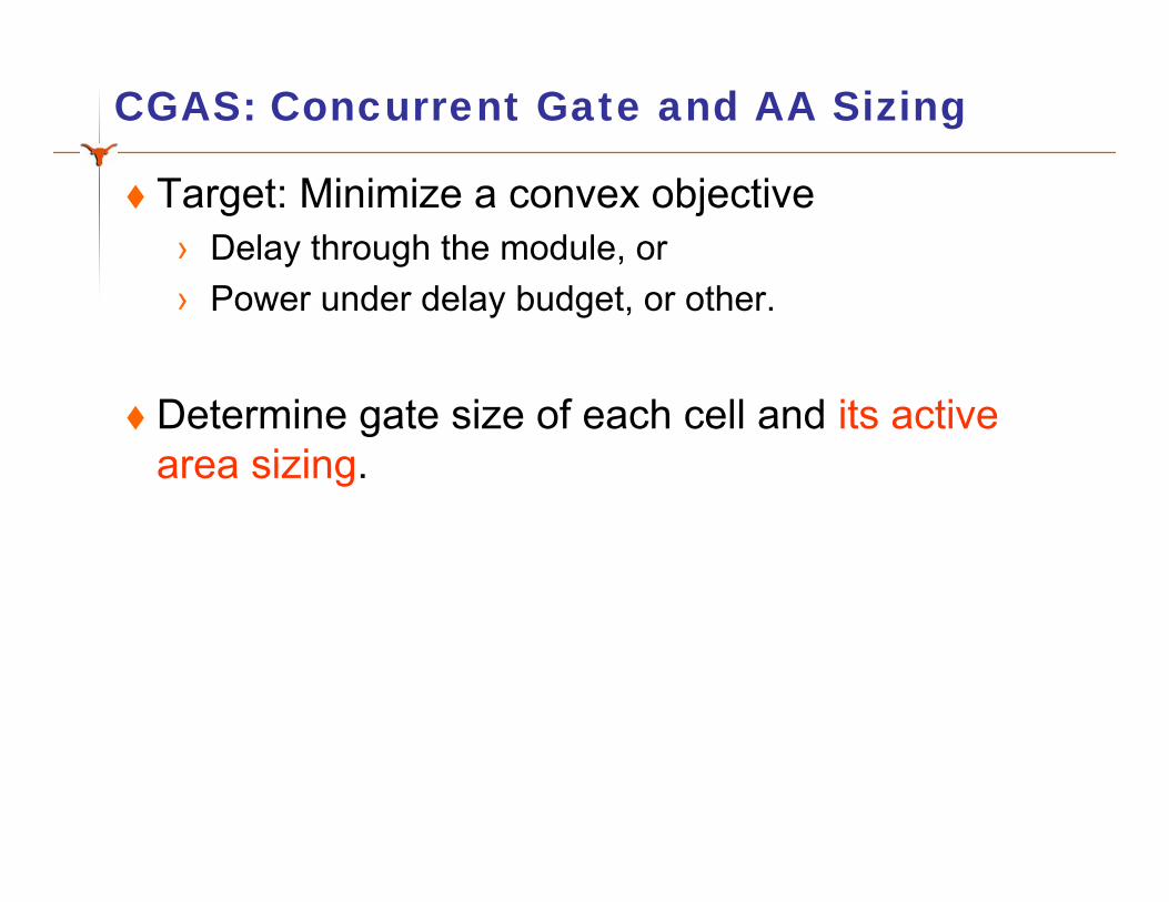
Target: Minimize a convex objective› Delay through the module, or› Power under delay budget, or other.
Determine gate size of each cell and its active area sizing.
CGAS: Formulation
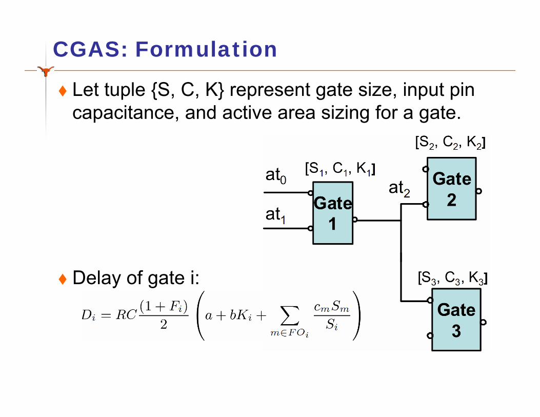
Let tuple {S, C, K} represent gate size, input pin capacitance, and active area sizing for a gate.
Delay of gate i:

CGAS: Formulation
Are all constraints convex?› All except first are convex trivially.› First can be proven to be posynomial (see paper)
as long as fitting parameter A is >= 1

Results [ CGAS on IWLS benchmarks ]
0.910.1Average:1.511.04004492007C53151.313.92332703759des0.610.2199222628vda0.39.8236262481large0.46.46877342581C75520.58.72953231163k20.210.7159178149frg10.49.0309340502C8803.211.0117513203316C6288
% ∆Cap.
%PerfImprv
DelayCGAS
DelayGS
NumGates
Bench
More than 10% reduction with CGAS over traditional Gate Sizing (GS)Less than 1% capacitance increase due to larger active areaNote: All delay values are multiples of RC
Outline
Intro. to source/drain (S/D) SiGe technology
Cell Delay Model Derivation
AA aware Optimal Repeater Insertion (ORI)
Concurrent AA and Gate Sizing
Conclusions

Conclusions
When moving to S/D SiGe, physical synthesis must be revisited to extract maximum benefit.
Proposed SiGe AA sizing aware RC model with cap increase and PMOS RON decrease.
For long global interconnects, with SiGe AA sizing of repeaters, delay reduced further by 9%.
Conclusions (contd…)
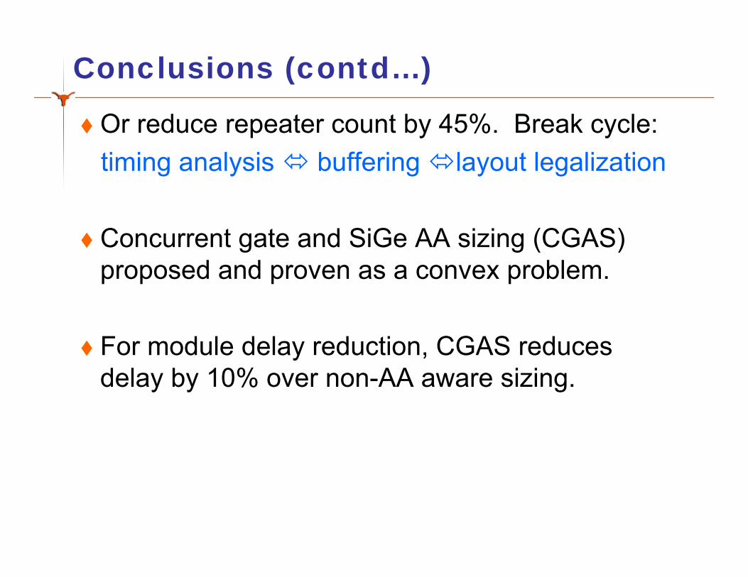
Or reduce repeater count by 45%. Break cycle:timing analysis buffering layout legalization
Concurrent gate and SiGe AA sizing (CGAS) proposed and proven as a convex problem.
For module delay reduction, CGAS reduces delay by 10% over non-AA aware sizing.
References
“Scalability of the SiGe S/D technology for the 45-nm technology node and beyond,” in IEEE Transactions on Electron Devices, July 2006.L.Washington et al., “pMOSFET with 200% mobility enhancement induced by multiple stressors,” Electron Device Letters, IEEE, vol. 27, no. 6, pp. 511–513,June 2006S. Boyd et al. , Convex Optimization. Cambridge Univ. Press, March 2004.

NotationIn the rest of the work:
Increasing the active area of a gate by K times reduces its PMOS’s resistance by F times. These are related by the formula
A = 1 : PMOS resistance independent of KA < 1 : PMOS resistance increases with higher KA > 1 : PMOS resistance reduces with higher K
In our curve fit, A = 3.4

Optimal K Value
Depends on fabrication technology› i.e. on single fitting parameter A
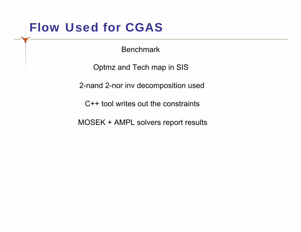
Flow Used for CGASBenchmark
Optmz and Tech map in SIS
2-nand 2-nor inv decomposition used
C++ tool writes out the constraints
MOSEK + AMPL solvers report results
Link to the paper

S C DG W
L LppLpp
S C DG W
L L’ppL’pp

AA Sizing Aware Repeater Insertion
Source SinkR R R R R
RepeaterInsertionLength
Per Unit ResistancePer Unit Capacitance# Of RepeatersInterconnect LengthRepeater Sizing
RwCwMLS