streaming encryption for a secure wavelength and time ... · streaming encryption for a secure...
TRANSCRIPT

Streaming Encryption for a Secure Wavelength and TimeDomain Hopped Optical Network
Herwin Chan, Alireza Hodjat, Jun Shi, Richard Wesel, Ingrid Verbauwhede{herwin, ahodjat, junshi, wesel, ingrid} @ ee.ucla.edu
Electrical Engineering DepartmentUniversity of California, Los Angeles
Abstract
This paper describes a working implementation of astreaming encryption system for optical networks. The10 Gbps data stream is encrypted on the physical levelin both the wavelength and time domains. Security isobtained by applying a strong pseudo-random hoppingpattern to both. The AES algorithm in counter mode isused to control the switches that implement the hoppingpermutations. Because of the high throughputrequirements, aggressive parallelizing and pipeliningtechniques are used to achieve data rates of 10 Gbps.
The core logic of the system was implemented on theVirtex2-XC2V1000 FPGA. Using four FPGA boardsand four serializer and deserializer chips, a secureswitch of 4 users over 4 wavelengths can be realized,resulting in a total throughput of 10 Gbps. This systemis important as a platform for further research in thearea of secure optical networks.
1. Introduction
Physical layer security is one way of increasing thesecurity of an entire network. In such a system, all datafrom a source is encrypted before being put onto thenetwork. This paper describes an electronicimplementation of a streaming encryption system foroptical networks. The basic concept involves thescrambling of the incoming bits of a datastream in boththe frequency and time domains. High throughputs canbe achieved using aggressive parallelization andpipelining techniques. Previous work in this area hasfocused on design of optical components which willperform the coding in the optical domain [1, 2]. Suchsystems have not yet been realized due to designcomplexity of the multi-wavelength hardwarecomponents.
Other systems focus on development of streamingencryption coprocessors [3, 4]. Because suchapproaches do not take a system view, interfacingoverheads can severely degrade performance throughput.The design of our system incurs minimal overhead andcan therefore achieve much higher throughput demands.
The main contribution of this paper is a descriptionof a functional and scalable streaming encryptionsystem. In our system, the cryptographically strongencryption algorithm, AES, is used in the counter modeto generate a pseudo-random bit stream. This bit streamis used as control signals which directly permute thedata stream through a switch matrix. By implementingthe complex logic of the code generator outside thedatapath, high rates can be achieved. A further benefitof this architecture is that the level of security can beeasily scaled by varying the rate of the code generator.
Section 2 describes the main coding strategy used inthe security system and defines the CDMA concept ofthe optical links. Section 3 then describes the overallarchitecture of this system and how different units ofthis system were implemented using the FPGA platform.Section 4 presents the complete system integration ofthe proposed security scheme. Section 5 discusses theperformance and cost of such a system and is followedby the conclusion in section 6.
2. Optical CMDA concept
Code Division Multiple Access, (CDMA), has beenrecognized to provide efficiency, security, and multi-access benefits in wireless communications. This hastriggered interest in providing similar advantages foroptical communication systems. Our encryption systemtakes the basic ideas of CDMA and implements it on topof the traditional Wave Division Multiplexing (WDM)system used in optics.
In traditional WDM, the input data stream isdemultiplexed to be transmitted on a number ofwavelengths (Figure 1a). If each wavelength representsthe data of an individual user, an attacker need onlylook at this one wavelength to understand theinformation.
In our proposed coding scheme, this data stream isbroken up into frames of N bits by M wavelengths(Figure 1b). Each frame contains NxM elementsrepresenting a unique time-wavelength position. Thecoding scheme will make a random permutation of theseelements for each time frame. This means both theorder of the bits in a stream and the wavelength inwhich it is transmitted may change.
Proceedings of the International Conference on Information Technology: Coding and Computing (ITCC’04) 0-7695-2108-8/04 $ 20.00 © 2004 IEEE

Transmitter Receiver
1 2 3 4
1 2 3 4
1 2 3 4
1 2 3 4
1 2 3 4
1 2 3 4
1 2 3 4
1 2 3 4
1 2 3 4
1 2 3 4
1 2 3 4
1 2 3 4
1 2 4 1
2 2 3 2
4 3 3 4
1 4 3 1
12 4
1
2
2
1 2
4
3 3
4
3
4
31
2 2 2 4
34
3
2
34
1
4
11 31
Transmitter Receiver
(a) Traditional WDM
(b) Time – Wavelength Domain Coding
Figure 1. Time-wavelength coding compared totraditional WDM transmission scheme
The security of the system depends on the quality ofthe random permutations. A strong pseudo-randomnumber generator, based on the AES algorithm in
counter mode is chosen to control the hopping patterns.Important for this is that the key is kept secret and thatthe initial seed is non-repeating.
3. Implementation
This section presents the overall architecture and theimplementation of the proposed security scheme. TheFPGA devices are used to implement the hardware unitsof the overall architecture.
3.1. System architecture
The demonstration setup encrypts and decrypts adata stream at a data rate of 10 Gbits/s. Data istransmitted through a single fiber optic cable carryingsignals modulated with four separate wavelengths. Thewidth of the data frame is 4 bits. This means that 16!unique permutations are possible for each frame.
Figure 2. Schematic view of (a) encryption and (b) decryption systems
1:4
Detector
λ1
λ2
λ3
Detector
Detector
Detector
User 1
155MHz
1:16
1:16
1:16
1:16
16:1
16:1
16:1
16:1
User 2
User 3
User 4λ4
155MHz
2.5Gbps
User 1
User 2
User 3
User 4
4:1
Modulator
Modulator
Modulator
Modulator
λ1
λ2Fiber
1:16
1:16
1:16
1:16
16:1
16:1
16:1
16:1
2.5Gbps
λ4
λ3
Switch MatrixProt.frame
Code Gen
Switch MatrixProt.frame
Code Gen
Demultiplexers FPGAs Multiplexers Optics Demultiplexers FPGAs Multiplexers
(a) (b)
Proceedings of the International Conference on Information Technology: Coding and Computing (ITCC’04) 0-7695-2108-8/04 $ 20.00 © 2004 IEEE

Figure 2a shows a high level description of theencryption system. Four high speed data lines (2.5Gbps) enter into the encryption block. They are de-serialized to 155 Mbps so that the processing can beperformed in the digital domain. A series of 16x16switches controlled by a code generator is used toproduce a random permutation of the inputs. Outputsfrom the switches are then serialized and modulatedbefore being transported out through a fiber connection.
The high level description of the decryption system isshown in Figure 2b. On the decryption side, the oppositeoperations must be done. However, it must be ensuredthat the code generators produce a synchronized andcorresponding code in order for the original data streamsto be recovered.
Serialization and de-serialization is performed bydiscrete electronic components. Its main role is toparallelize the input data stream to a manageable rate.
FPGA’s are used to implement the switchingfunctions and provide the pseudo-random codegeneration and synchronization. Modulation anddemodulation of the data signals are performed by off theshelf optical components.
3.2. FPGA implementation
The Virtex2-XC2V1000 FPGA from Xilinx was usedas the platform for the encryption and decryption units.This provides us with the necessary speed while beingprogrammable so that different architectures and featurescan be added to the system easily.
Figure 3 shows the overall architecture of the digitalencryption unit implemented on the FPGA. It has thefollowing main components: switching matrix, codegenerator unit, and protocol unit. The followingsubsections describe the details of each unit in thissecurity system as well as the token passing techniquewhich synchronizes them.
PLL
Switching Matrix
Delay Module
Code Generator
System clock
LV
DS
Output
LV
DS
Input
Protocol
Input clock
Input data
Output clock
Output data
Figure 3. Functional blocks in FPGAencryption
3.2.1. Switch matrix. The switching matrix iscomposed of a network of 2x2 switches which allows theoutput to be any permutation of the input. Figure 4shows how the 56 switches are connected in a Benesnetwork [5]. Each of these switches is controlled by asignal coming from the code generator. New control bitsare produced each clock cycle.
The basic building block of the switch matrix is the2x2 switch. A register is present at each output of thisswitch to ensure that the FPGA can be used at a highclock rate. This pipelining allows for high throughputwith the side affect of increased latency.
Because data path pipelining is introduced by puttingregisters in the switches, the control signals for theswitches must also be appropriately delayed. Figure 4shows how such a scheme should be implemented duringencryption.
c7
c6
c5
c4
c3
c2
c1
c0
c15
c14
c13
c12
c11
c10
c9
c8
c23
c22
c21
c20
c19
c18
c17
c16
c31
c30
c29
c28
c27
c26
c25
c24
c39
c38
c37
c36
c35
c34
c33
c32
c47
c46
c45
c44
c43
c42
c41
c40
c55
c54
c53
c52
c51
c50
c49
c48
[c0, c1, c2, …, c53, c54, c55]Code Generator
z 2z 3z 4z 5z 6z
Figure 4. Switch matrix configuration forencryption
During decryption, the control signals must be flippedso that it looks like a mirror image of the encryptionstructure. This is so that the code signals would matchproperly and the original data streams can be recoveredat the output.
3.2.2. Code generator. The code generator unit isresponsible for generating the pseudo-random numberswhich will act as control signals to the switches in theswitching matrix. The following two approaches areconsidered for this purpose.
3.2.2.1. AES in the counter mode of operation. Inorder to generate cryptographically secure randomnumbers, the Advanced Encryption Standard [6] can beused. Figure 5 shows how the AES algorithm can be
Proceedings of the International Conference on Information Technology: Coding and Computing (ITCC’04) 0-7695-2108-8/04 $ 20.00 © 2004 IEEE
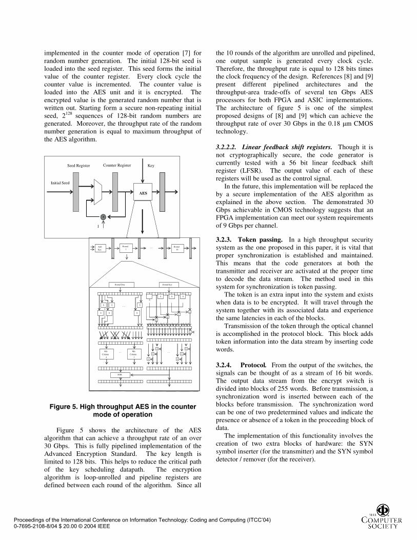
implemented in the counter mode of operation [7] forrandom number generation. The initial 128-bit seed isloaded into the seed register. This seed forms the initialvalue of the counter register. Every clock cycle thecounter value is incremented. The counter value isloaded into the AES unit and it is encrypted. Theencrypted value is the generated random number that iswritten out. Starting form a secure non-repeating initialseed, 2128 sequences of 128-bit random numbers aregenerated. Moreover, the throughput rate of the randomnumber generation is equal to maximum throughput ofthe AES algorithm.
Figure 5. High throughput AES in the countermode of operation
Figure 5 shows the architecture of the AESalgorithm that can achieve a throughput rate of an over30 Gbps. This is fully pipelined implementation of theAdvanced Encryption Standard. The key length islimited to 128 bits. This helps to reduce the critical pathof the key scheduling datapath. The encryptionalgorithm is loop-unrolled and pipeline registers aredefined between each round of the algorithm. Since all
the 10 rounds of the algorithm are unrolled and pipelined,one output sample is generated every clock cycle.Therefore, the throughput rate is equal to 128 bits timesthe clock frequency of the design. References [8] and [9]present different pipelined architectures and thethroughput-area trade-offs of several ten Gbps AESprocessors for both FPGA and ASIC implementations.The architecture of figure 5 is one of the simplestproposed designs of [8] and [9] which can achieve thethroughput rate of over 30 Gbps in the 0.18 �m CMOStechnology.
3.2.2.2. Linear feedback shift registers. Though it isnot cryptographically secure, the code generator iscurrently tested with a 56 bit linear feedback shiftregister (LFSR). The output value of each of theseregisters will be used as the control signal.
In the future, this implementation will be replaced theby a secure implementation of the AES algorithm asexplained in the above section. The demonstrated 30Gbps achievable in CMOS technology suggests that anFPGA implementation can meet our system requirementsof 9 Gbps per channel.
3.2.3. Token passing. In a high throughput securitysystem as the one proposed in this paper, it is vital thatproper synchronization is established and maintained.This means that the code generators at both thetransmitter and receiver are activated at the proper timeto decode the data stream. The method used in thissystem for synchronization is token passing.
The token is an extra input into the system and existswhen data is to be encrypted. It will travel through thesystem together with its associated data and experiencethe same latencies in each of the blocks.
Transmission of the token through the optical channelis accomplished in the protocol block. This block addstoken information into the data stream by inserting codewords.
3.2.4. Protocol. From the output of the switches, thesignals can be thought of as a stream of 16 bit words.The output data stream from the encrypt switch isdivided into blocks of 255 words. Before transmission, asynchronization word is inserted between each of theblocks before transmission. The synchronization wordcan be one of two predetermined values and indicate thepresence or absence of a token in the proceeding block ofdata.
The implementation of this functionality involves thecreation of two extra blocks of hardware: the SYNsymbol inserter (for the transmitter) and the SYN symboldetector / remover (for the receiver).
Initial Seed
Round
10
Add
Key…Round
1
Round KeyRound Data
S
SS S
S S …
S
++
++
AES
+
1
KeySeed Register Counter Register
+
+
+
+
+
+
+
…Mix
Column
1
Mix
Column
4
…
XOR
SSS
Proceedings of the International Conference on Information Technology: Coding and Computing (ITCC’04) 0-7695-2108-8/04 $ 20.00 © 2004 IEEE

4. Complete system integration
Figure 6 shows the architectural diagram of the wholesystem. It includes all the elements that were shown inFigures 2 and 3. There is a total of 8 FPGA’s in thecomplete system. The serializer and deserializer units onboth the transmitter and receiver sides are integrated ontoa single board, indicated by SERDES. On the transmitterside the encrypted output of each serializer goes to theoptical modulator before combination to a single opticalfiber through the optical multiplexer. On the receiverside, optical data is first demultiplexed and demodulatedbefore being converted back to an electrical signal.
FGPA FPGA
SERDES
FPGA FPGA
Opt. tx
Opt. tx
Opt. tx
Opt. tx
Optmux
FPGAFPGA
SERDES
FPGAFPGA
Opt. rx
Opt. rx
Opt. rx
Opt.rx
Opt.dmux
Figure 6. Component architecture ofdemonstration system
5. Results
Serialization and deserialization of the four 2.5Gbpsdata streams were accomplished with commercial off theshelf SERDES components. It communicates with theXillinx FPGA, which performs the actualencryption/decryption, through an LVDS interface.
Table 1 shows the implementation cost of each blockimplemented in the FPGA. Note that though theimplementation costs are very low in such animplementation, much of the area in the future will betaken up by our secure AES code generator. In addition,system size is expected to shrink in the future as theSERDES functions are integrated onto the FPGA.
Table 1. Implementation cost ofencryption/decryption
The circuit speed is within the requirements neededfor 10 Gbps operation and can currently sustain rates ofup to 13 Gbps. Futher optimizations of the protocolblocks can increase this throughput even more.
6. Conclusion
A working implementation of a secure streamingencryption system is described in this paper. Highthroughputs are achieved by using a code generator todirectly control the datapath of the datastream.Aggressive pipelining and parallelization were used toreduce clock speeds to a manageable level.
Because of its small size and flexible implementationplatform, it is a good platform in which to explore theproperties of such systems. Future work will focus oncomponent consolidation and studies on systemscalability. As a research platform, it can be used tostudy higher level issues such as protocol developmentand fault tolerant architectures.
Acknowledgement
This material is based upon work supported by theSpace and Naval Warfare Systems Center - San Diegounder contract No.N66001-02-1-8938. The authorswould like to acknowledge the funding of this project.
References
[1] S. Yegnanarayanan, A. S. Bhushan, and B. Jalali, “Fastwavelength-hopping time-spreading encoding/decoding foroptical CDMA”, IEEE Photonics Technology Letters, vol.12,(no.5), IEEE, May 2000.
[2] C. F. Lam and E. Yablonovitch, “A fast wavelengthhopped CDMA system for secure optical communications”,Proceedings of the SPIE - Dallas, TX, SPIE-Int. Soc. Opt. Eng,1998.
[3] D. Carlson et al, “A high performance SSL IPSECprotocol aware security processor”, ISSCC 2003.
[4] D. K. Y. Tong et al, “A system level implementation ofRijndael on a memory-slot based FPGA card”, IEEEConference on Field-Programmable Technology, December2002.
[5] C. Chang and R. Melhem, "Arbitrary Size BenesNetworks", Parallel Processing Letters, vol 7, no 3, pp 279-284(1997).
[6] National Institute of Standards and Technology (U.S.),Advanced Encryption Standard. Available at:http://csrc.nist.gov/publication/drafts/dfips-AES.pdf
[7] M. Dworkin, SP 800-38A 2001, “Recommendation forBlock Cipher Modes of Operations”, December 01.
[8] A. Hodjat, I. Verbauwhede, “Speed-Area Trade-off for 10to 100 Gbits/s throughput AES processor”, 37th AsilomarConference on Signals, Systems, and Computers, November2003.
[9] A. Hodjat, I. Verbauwhede, “Minimum Area Cost for a 30to 70 Gbits/s AES Processor”, IEEE Computer Society AnnualSymposium on VLSI, February 2004.
Block Area(slices)
Speed(ns)
Switching matrix 155 2.1Protocol (encryption) 54 3.3Protocol (decryption) 29 4.9Code Generator (LFSR) 29 2.5
Proceedings of the International Conference on Information Technology: Coding and Computing (ITCC’04) 0-7695-2108-8/04 $ 20.00 © 2004 IEEE