stencil printing of small apertures - surface-mount … · stencil printing of small apertures ......
TRANSCRIPT
Stencil Printing of Small Apertures
William E. Coleman Ph.D.
Photo Stencil, Colorado Springs, CO
Abstract
Many of the latest SMT assemblies for hand held devices like cell phones present a challenge to process and manufacturing
engineers with the introduction of miniature components such as .3 mm CSP and uBGA devices as well as 0201 and 01005
chip component devices. Printing these miniature devices along with more conventional SMT devices like .5mm QFP’s and
0603 and 0805 passives, in addition to RF shields is a challenge. Whereas a 4mil (100 micron) or 5 mil (125 micron) thick
stencil provides good paste transfer for the normal SMT devices, stencils with this thickness have very low Area Ratios for
the miniature devices. For example a .3mm CSP with a 7.5 mil (190 micron) has a .47 Area Ratio for a 4 mil thick stencil.
This paper will examine stencil technologies (including Laser and Electroform), Aperture Wall coatings (including Nickel-
Teflon coatings and Nano-coatings), and how these parameters influence paste transfer for miniature devices with Area
Ratios less than the standard recommended lower limit of .5. A matrix of print tests will be utilized to compare paste transfer
and measure the effectiveness of the different stencil configurations. Area Ratios ranging from .32 to .68 will be
investigated.
Introduction
SMT assembly is faced with a common challenge. As components get smaller and smaller, it is difficult to print solder paste
to satisfy both components. On the one hand the large components require more solder paste volume for sufficient solder
fillets after reflow. If this same stencil is used to print paste for the small components the apertures are so small that poor
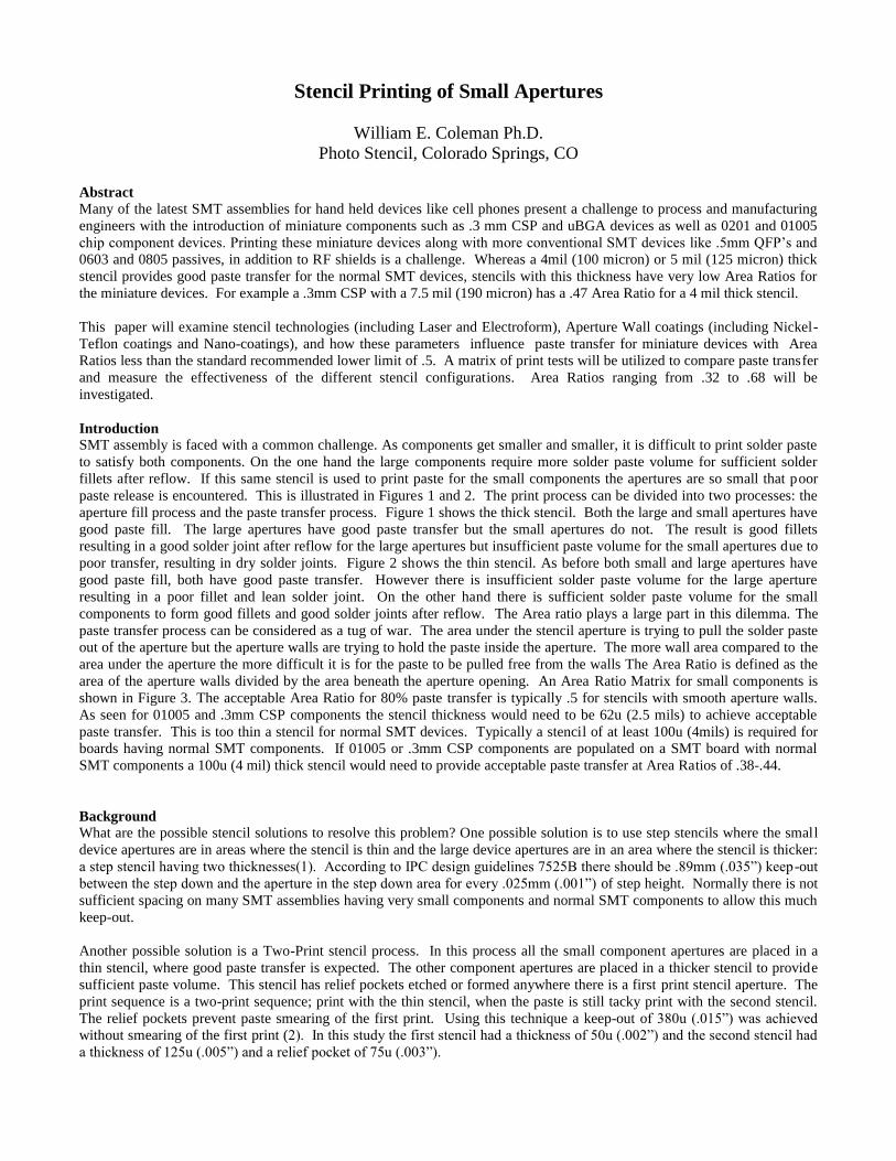
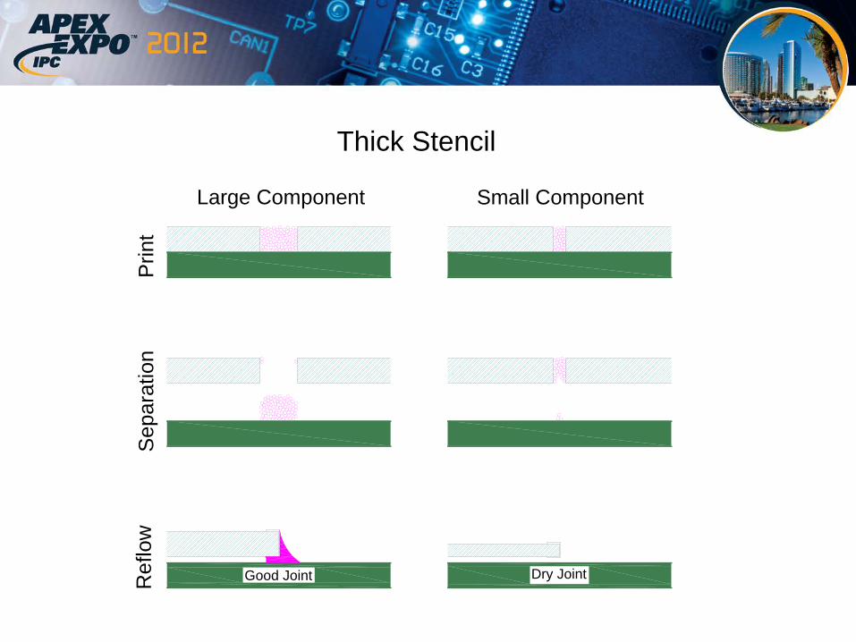
paste release is encountered. This is illustrated in Figures 1 and 2. The print process can be divided into two processes: the
aperture fill process and the paste transfer process. Figure 1 shows the thick stencil. Both the large and small apertures have
good paste fill. The large apertures have good paste transfer but the small apertures do not. The result is good fillets
resulting in a good solder joint after reflow for the large apertures but insufficient paste volume for the small apertures due to
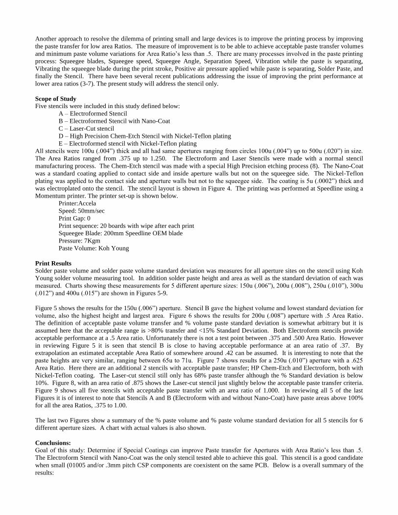
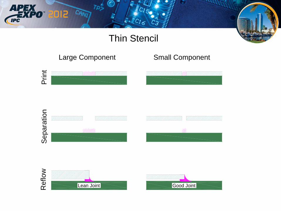
poor transfer, resulting in dry solder joints. Figure 2 shows the thin stencil. As before both small and large apertures have
good paste fill, both have good paste transfer. However there is insufficient solder paste volume for the large aperture
resulting in a poor fillet and lean solder joint. On the other hand there is sufficient solder paste volume for the small
components to form good fillets and good solder joints after reflow. The Area ratio plays a large part in this dilemma. The
paste transfer process can be considered as a tug of war. The area under the stencil aperture is trying to pull the solder paste
out of the aperture but the aperture walls are trying to hold the paste inside the aperture. The more wall area compared to the
area under the aperture the more difficult it is for the paste to be pulled free from the walls The Area Ratio is defined as the
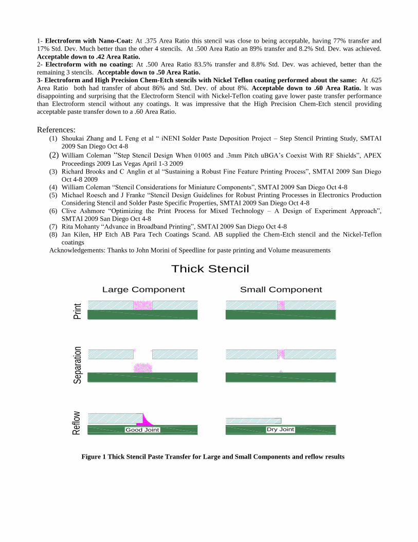
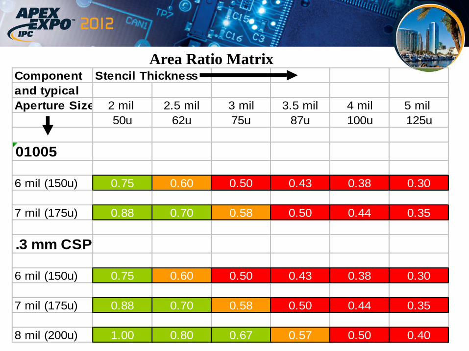
area of the aperture walls divided by the area beneath the aperture opening. An Area Ratio Matrix for small components is
shown in Figure 3. The acceptable Area Ratio for 80% paste transfer is typically .5 for stencils with smooth aperture walls.
As seen for 01005 and .3mm CSP components the stencil thickness would need to be 62u (2.5 mils) to achieve acceptable
paste transfer. This is too thin a stencil for normal SMT devices. Typically a stencil of at least 100u (4mils) is required for
boards having normal SMT components. If 01005 or .3mm CSP components are populated on a SMT board with normal
SMT components a 100u (4 mil) thick stencil would need to provide acceptable paste transfer at Area Ratios of .38-.44.
Background
What are the possible stencil solutions to resolve this problem? One possible solution is to use step stencils where the small
device apertures are in areas where the stencil is thin and the large device apertures are in an area where the stencil is thicker:
a step stencil having two thicknesses(1). According to IPC design guidelines 7525B there should be .89mm (.035”) keep-out
between the step down and the aperture in the step down area for every .025mm (.001”) of step height. Normally there is not
sufficient spacing on many SMT assemblies having very small components and normal SMT components to allow this much
keep-out.
Another possible solution is a Two-Print stencil process. In this process all the small component apertures are placed in a
thin stencil, where good paste transfer is expected. The other component apertures are placed in a thicker stencil to provide
sufficient paste volume. This stencil has relief pockets etched or formed anywhere there is a first print stencil aperture. The
print sequence is a two-print sequence; print with the thin stencil, when the paste is still tacky print with the second stencil.
The relief pockets prevent paste smearing of the first print. Using this technique a keep-out of 380u (.015”) was achieved
without smearing of the first print (2). In this study the first stencil had a thickness of 50u (.002”) and the second stencil had
a thickness of 125u (.005”) and a relief pocket of 75u (.003”).
Another approach to resolve the dilemma of printing small and large devices is to improve the printing process by improving
the paste transfer for low area Ratios. The measure of improvement is to be able to achieve acceptable paste transfer volumes
and minimum paste volume variations for Area Ratio’s less than .5. There are many processes involved in the paste printing
process: Squeegee blades, Squeegee speed, Squeegee Angle, Separation Speed, Vibration while the paste is separating,
Vibrating the squeegee blade during the print stroke, Positive air pressure applied while paste is separating, Solder Paste, and
finally the Stencil. There have been several recent publications addressing the issue of improving the print performance at
lower area ratios (3-7). The present study will address the stencil only.
Scope of Study
Five stencils were included in this study defined below:
A – Electroformed Stencil
B – Electroformed Stencil with Nano-Coat
C – Laser-Cut stencil
D – High Precision Chem-Etch Stencil with Nickel-Teflon plating
E – Electroformed stencil with Nickel-Teflon plating
All stencils were 100u (.004”) thick and all had same apertures ranging from circles 100u (.004”) up to 500u (.020”) in size.
The Area Ratios ranged from .375 up to 1.250. The Electroform and Laser Stencils were made with a normal stencil
manufacturing process. The Chem-Etch stencil was made with a special High Precision etching process (8). The Nano-Coat
was a standard coating applied to contact side and inside aperture walls but not on the squeegee side. The Nickel-Teflon
plating was applied to the contact side and aperture walls but not to the squeegee side. The coating is 5u (.0002”) thick and
was electroplated onto the stencil. The stencil layout is shown in Figure 4. The printing was performed at Speedline using a
Momentum printer. The printer set-up is shown below.
Printer:Accela
Speed: 50mm/sec
Print Gap: 0
Print sequence: 20 boards with wipe after each print
Squeegee Blade: 200mm Speedline OEM blade
Pressure: 7Kgm
Paste Volume: Koh Young
Print Results
Solder paste volume and solder paste volume standard deviation was measures for all aperture sites on the stencil using Koh
Young solder volume measuring tool. In addition solder paste height and area as well as the standard deviation of each was
measured. Charts showing these measurements for 5 different aperture sizes: 150u (.006”), 200u (.008”), 250u (.010”), 300u
(.012”) and 400u (.015”) are shown in Figures 5-9.
Figure 5 shows the results for the 150u (.006”) aperture. Stencil B gave the highest volume and lowest standard deviation for
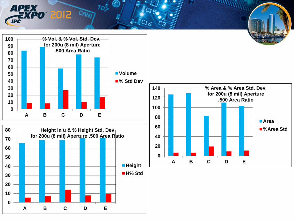
volume, also the highest height and largest area. Figure 6 shows the results for 200u (.008”) aperture with .5 Area Ratio .
The definition of acceptable paste volume transfer and % volume paste standard deviation is somewhat arbitrary but it is
assumed here that the acceptable range is >80% transfer and <15% Standard Deviation. Both Electroform stencils provide
acceptable performance at a .5 Area ratio. Unfortunately there is not a test point between .375 and .500 Area Ratio. However
in reviewing Figure 5 it is seen that stencil B is close to having acceptable performance at an area ratio of .37. By
extrapolation an estimated acceptable Area Ratio of somewhere around .42 can be assumed. It is interesting to note that the
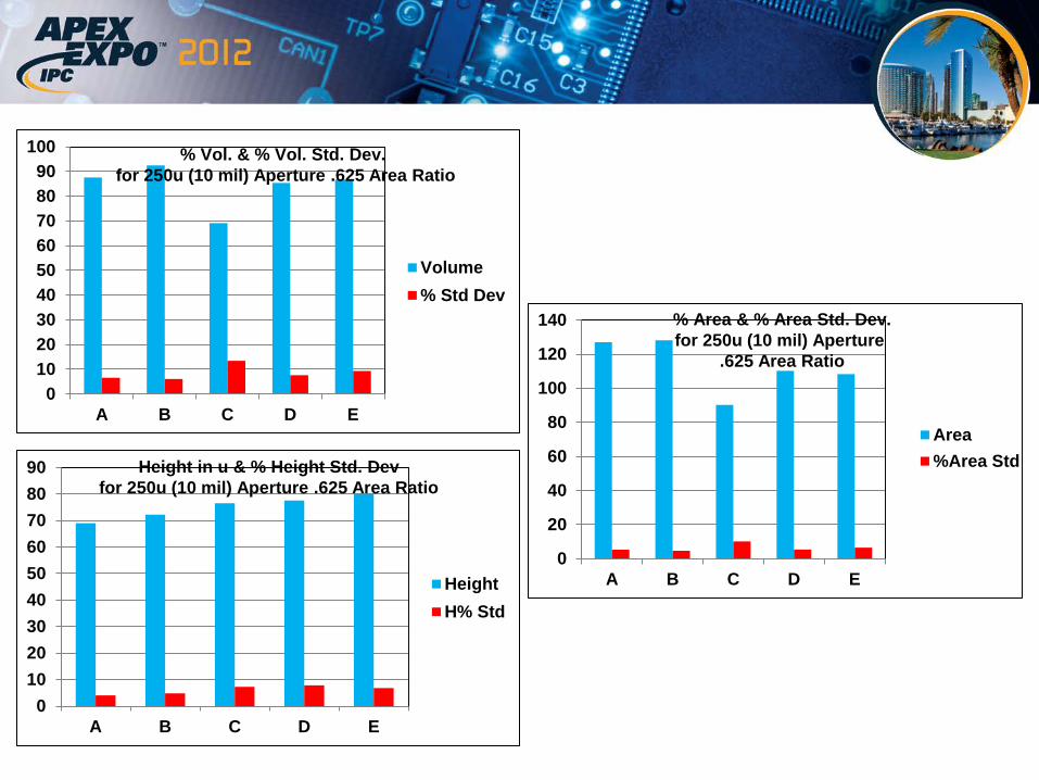
paste heights are very similar, ranging between 65u to 71u. Figure 7 shows results for a 250u (.010”) aperture with a .625
Area Ratio. Here there are an additional 2 stencils with acceptable paste transfer; HP Chem-Etch and Electroform, both with
Nickel-Teflon coating. The Laser-cut stencil still only has 68% paste transfer although the % Standard deviation is below
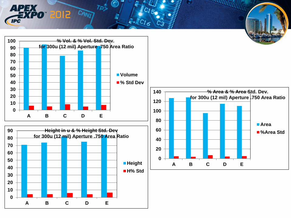
10%. Figure 8, with an area ratio of .875 shows the Laser-cut stencil just slightly below the acceptable paste transfer criteria.
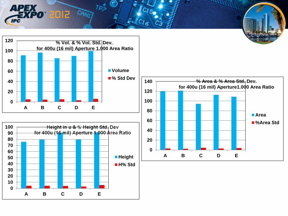
Figure 9 shows all five stencils with acceptable paste transfer with an area ratio of 1.000. In reviewing all 5 of the last
Figures it is of interest to note that Stencils A and B (Electroform with and without Nano-Coat) have paste areas above 100%
for all the area Ratios, .375 to 1.00.
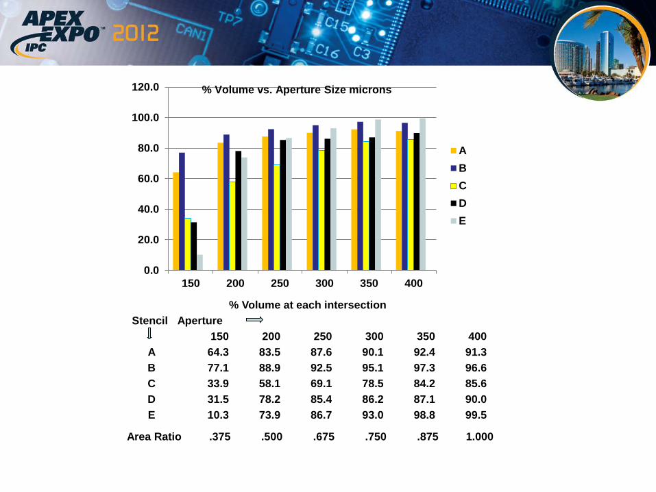
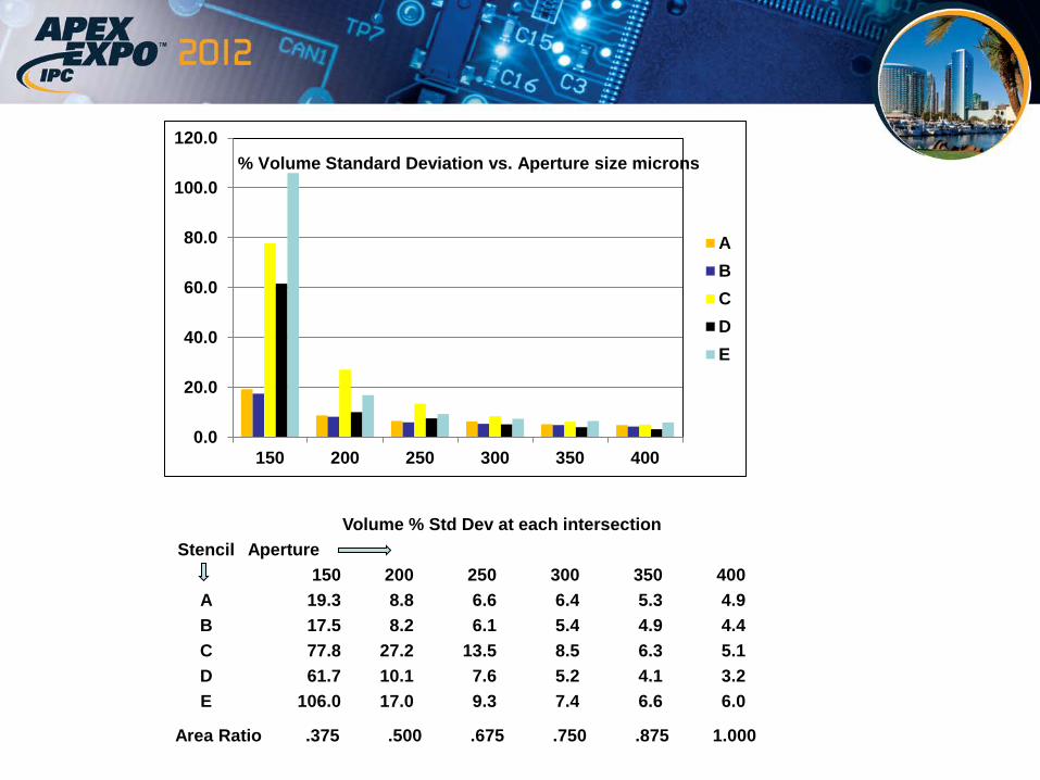
The last two Figures show a summary of the % paste volume and % paste volume standard deviation for all 5 stencils for 6
different aperture sizes. A chart with actual values is also shown.
Conclusions: Goal of this study: Determine if Special Coatings can improve Paste transfer for Apertures with Area Ratio’s less than .5.
The Electroform Stencil with Nano-Coat was the only stencil tested able to achieve this goal. This stencil is a good candidate
when small (01005 and/or .3mm pitch CSP components are coexistent on the same PCB. Below is a overall summary of the
results:
1- Electroform with Nano-Coat: At .375 Area Ratio this stencil was close to being acceptable, having 77% transfer and
17% Std. Dev. Much better than the other 4 stencils. At .500 Area Ratio an 89% transfer and 8.2% Std. Dev. was achieved.
Acceptable down to .42 Area Ratio. 2- Electroform with no coating: At .500 Area Ratio 83.5% transfer and 8.8% Std. Dev. was achieved, better than the
remaining 3 stencils. Acceptable down to .50 Area Ratio.
3- Electroform and High Precision Chem-Etch stencils with Nickel Teflon coating performed about the same: At .625
Area Ratio both had transfer of about 86% and Std. Dev. of about 8%. Acceptable down to .60 Area Ratio. It was
disappointing and surprising that the Electroform Stencil with Nickel-Teflon coating gave lower paste transfer performance
than Electroform stencil without any coatings. It was impressive that the High Precision Chem-Etch stencil providing
acceptable paste transfer down to a .60 Area Ratio.
References: (1) Shoukai Zhang and L Feng et al “ iNENI Solder Paste Deposition Project – Step Stencil Printing Study, SMTAI
2009 San Diego Oct 4-8
(2) William Coleman “Step Stencil Design When 01005 and .3mm Pitch uBGA’s Coexist With RF Shields”, APEX
Proceedings 2009 Las Vegas April 1-3 2009 (3) Richard Brooks and C Anglin et al “Sustaining a Robust Fine Feature Printing Process”, SMTAI 2009 San Diego
Oct 4-8 2009
(4) William Coleman “Stencil Considerations for Miniature Components”, SMTAI 2009 San Diego Oct 4-8
(5) Michael Roesch and J Franke “Stencil Design Guidelines for Robust Printing Processes in Electronics Production
Considering Stencil and Solder Paste Specific Properties, SMTAI 2009 San Diego Oct 4-8
(6) Clive Ashmore “Optimizing the Print Process for Mixed Technology – A Design of Experiment Approach”,
SMTAI 2009 San Diego Oct 4-8
(7) Rita Mohanty “Advance in Broadband Printing”, SMTAI 2009 San Diego Oct 4-8
(8) Jan Kilen, HP Etch AB Para Tech Coatings Scand. AB supplied the Chem-Etch stencil and the Nickel-Teflon
coatings
Acknowledgements: Thanks to John Morini of Speedline for paste printing and Volume measurements
Figure 1 Thick Stencil Paste Transfer for Large and Small Components and reflow results
Good Joint Dry JointRef
low
Sep
arat
ion
Prin
t
Large Component Small Component
Thick Stencil
Lean Joint Good Joint
Thin Stencil
Small ComponentLarge Component
Ref
low
Prin
tS
epar
atio
n
Figure 2 Thin stencil Paste Transfer for Large and Small Components and reflow results
Green = OK Orange = Warning Red = Stop
Figure 3 Area Ratio Matrix For small SMT components
Component Stencil Thickness
and typical
Aperture Size 2 mil 2.5 mil 3 mil 3.5 mil 4 mil 5 mil
50u 62u 75u 87u 100u 125u
01005
6 mil (150u) 0.75 0.60 0.50 0.43 0.38 0.30
7 mil (175u) 0.88 0.70 0.58 0.50 0.44 0.35
.4mm CSP
6 mil (150u) 0.75 0.60 0.50 0.43 0.38 0.30
7 mil (175u) 0.88 0.70 0.58 0.50 0.44 0.35
8 mil (200u) 1.00 0.80 0.67 0.57 0.50 0.40
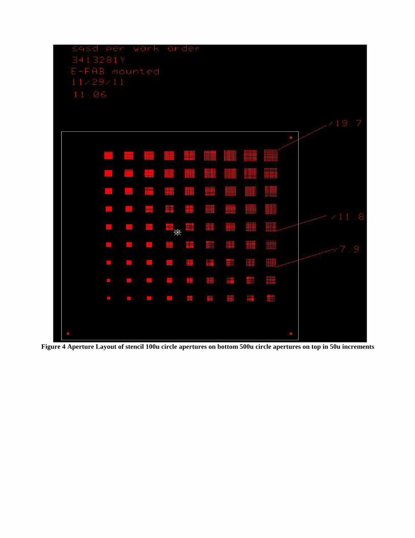
Figure 4 Aperture Layout of stencil 100u circle apertures on bottom 500u circle apertures on top in 50u increments
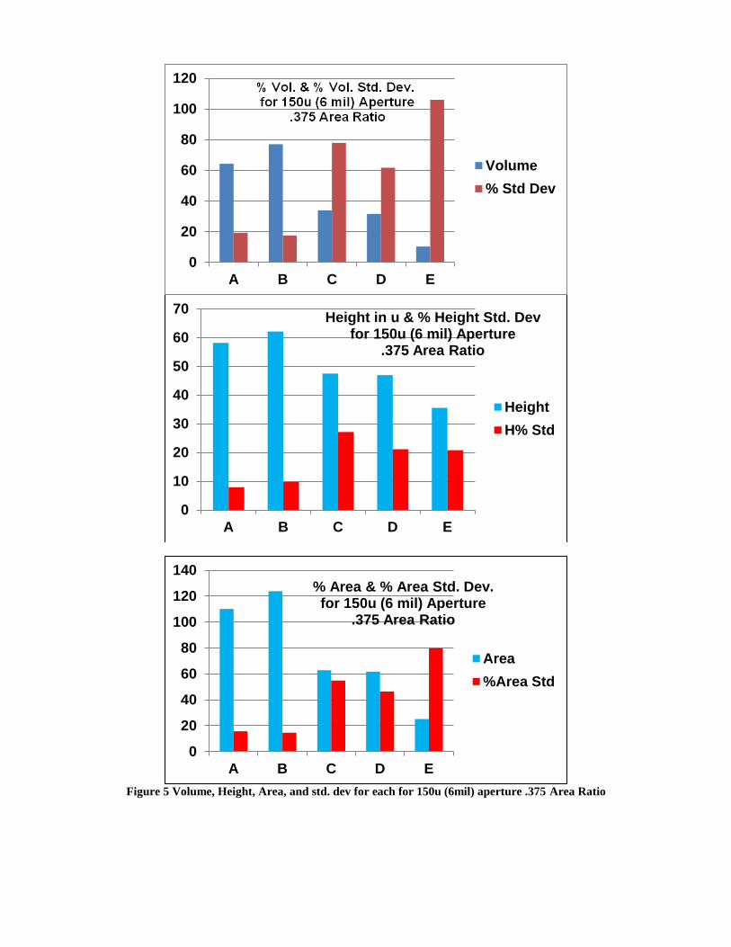
Figure 5 Volume, Height, Area, and std. dev for each for 150u (6mil) aperture .375 Area Ratio
0
20
40
60
80
100
120
A B C D E
Volume
% Std Dev
0
10
20
30
40
50
60
70
A B C D E
Height
H% Std
Height in u & % Height Std. Dev for 150u (6 mil) Aperture
.375 Area Ratio
0
20
40
60
80
100
120
140
A B C D E
Area
%Area Std
% Area & % Area Std. Dev. for 150u (6 mil) Aperture
.375 Area Ratio
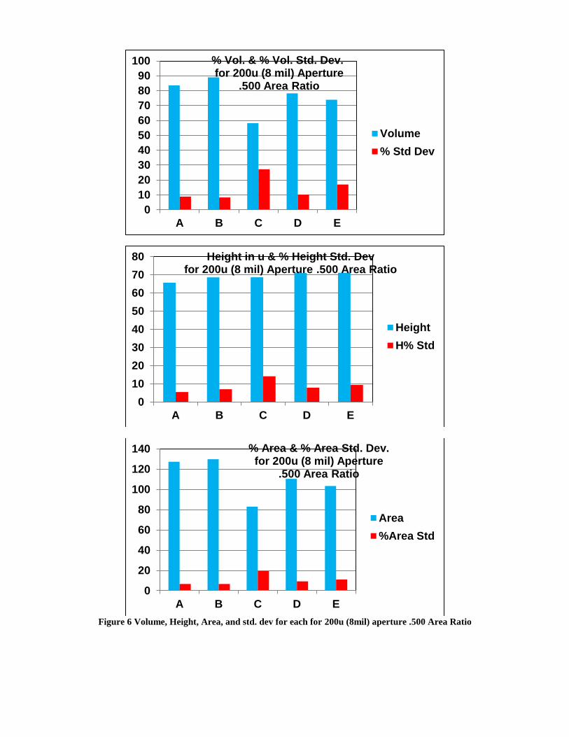
Figure 6 Volume, Height, Area, and std. dev for each for 200u (8mil) aperture .500 Area Ratio
0
10
20
30
40
50
60
70
80
90
100
A B C D E
Volume
% Std Dev
% Vol. & % Vol. Std. Dev. for 200u (8 mil) Aperture
.500 Area Ratio
0
10
20
30
40
50
60
70
80
A B C D E
Height
H% Std
Height in u & % Height Std. Dev for 200u (8 mil) Aperture .500 Area Ratio
0
20
40
60
80
100
120
140
A B C D E
Area
%Area Std
% Area & % Area Std. Dev. for 200u (8 mil) Aperture
.500 Area Ratio

Figure 7 Volume, Height, Area, and std. dev for each for 250u (10mil) aperture .625 Area Ratio
0
10
20
30
40
50
60
70
80
90
100
A B C D E
Volume
% Std Dev
% Vol. & % Vol. Std. Dev. for 250u (10 mil) Aperture .625 Area Ratio
0
10
20
30
40
50
60
70
80
90
A B C D E
Height
H% Std
Height in u & % Height Std. Dev for 250u (10 mil) Aperture .625 Area Ratio
0
20
40
60
80
100
120
140
A B C D E
Area
%Area Std
% Area & % Area Std. Dev. for 250u (10 mil) Aperture
.625 Area Ratio
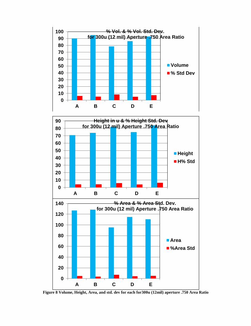
Figure 8 Volume, Height, Area, and std. dev for each for300u (12mil) aperture .750 Area Ratio
0
10
20
30
40
50
60
70
80
90
100
A B C D E
Volume
% Std Dev
% Vol. & % Vol. Std. Dev. for 300u (12 mil) Aperture .750 Area Ratio
0
10
20
30
40
50
60
70
80
90
A B C D E
Height
H% Std
Height in u & % Height Std. Dev for 300u (12 mil) Aperture .750 Area Ratio
0
20
40
60
80
100
120
140
A B C D E
Area
%Area Std
% Area & % Area Std. Dev. for 300u (12 mil) Aperture .750 Area Ratio
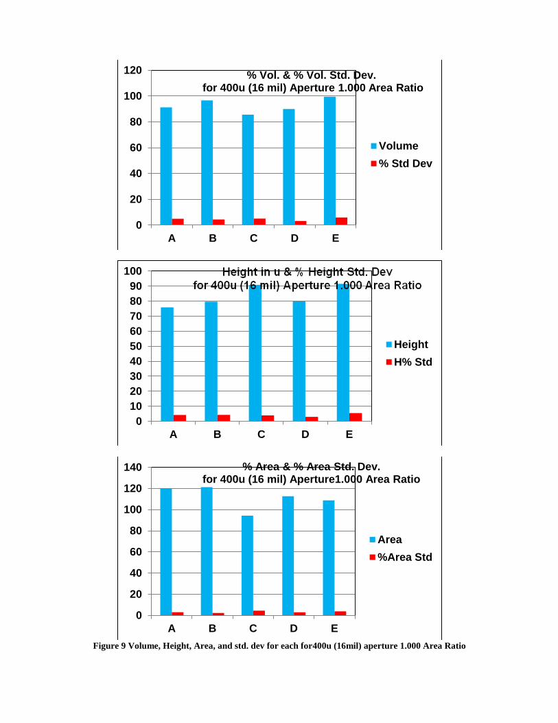
Figure 9 Volume, Height, Area, and std. dev for each for400u (16mil) aperture 1.000 Area Ratio
0
20
40
60
80
100
120
A B C D E
Volume
% Std Dev
% Vol. & % Vol. Std. Dev. for 400u (16 mil) Aperture 1.000 Area Ratio
0
10
20
30
40
50
60
70
80
90
100
A B C D E
Height
H% Std
0
20
40
60
80
100
120
140
A B C D E
Area
%Area Std
% Area & % Area Std. Dev. for 400u (16 mil) Aperture1.000 Area Ratio
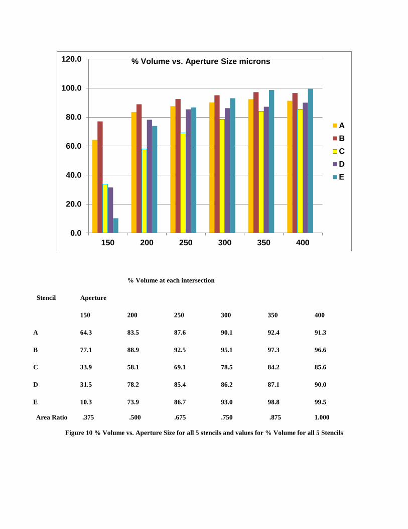
% Volume at each intersection
Stencil Aperture
150 200 250 300 350 400
A 64.3 83.5 87.6 90.1 92.4 91.3
B 77.1 88.9 92.5 95.1 97.3 96.6
C 33.9 58.1 69.1 78.5 84.2 85.6
D 31.5 78.2 85.4 86.2 87.1 90.0
E 10.3 73.9 86.7 93.0 98.8 99.5
Area Ratio .375 .500 .675 .750 .875 1.000
Figure 10 % Volume vs. Aperture Size for all 5 stencils and values for % Volume for all 5 Stencils
0.0
20.0
40.0
60.0
80.0
100.0
120.0
150 200 250 300 350 400
A
B
C
D
E
% Volume vs. Aperture Size microns
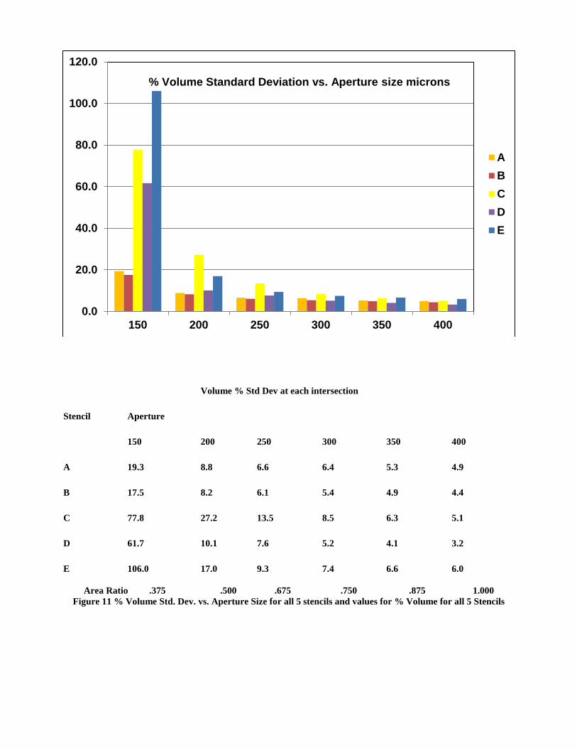
Volume % Std Dev at each intersection
Stencil Aperture
150 200 250 300 350 400
A 19.3 8.8 6.6 6.4 5.3 4.9
B 17.5 8.2 6.1 5.4 4.9 4.4
C 77.8 27.2 13.5 8.5 6.3 5.1
D 61.7 10.1 7.6 5.2 4.1 3.2
E 106.0 17.0 9.3 7.4 6.6 6.0
Area Ratio .375 .500 .675 .750 .875 1.000
Figure 11 % Volume Std. Dev. vs. Aperture Size for all 5 stencils and values for % Volume for all 5 Stencils
0.0
20.0
40.0
60.0
80.0
100.0
120.0
150 200 250 300 350 400
A
B
C
D
E
% Volume Standard Deviation vs. Aperture size microns
Stencil Printing of Small Apertures
William E. Coleman Ph.D.
Vice President Technology
Photo Stencil
Colorado Springs, CO
Stencil Printing of Small Apertures William E. Coleman Ph.D.
Photo Stencil, Colorado Springs, CO
• Problem: • Printing small devices (.3mm pitch CSP’s and 01005’s) at the same time as printing large devices (SMT connectors, QFP’s, and chip components).
• Why is this a problem: • Thin stencil needed for small devices for acceptable paste transfer (Area Ratio). • Thin Stencil gives insufficient paste volume large devices. • Thick Stencil gives insufficient paste transfer for small devices.
Good Joint Dry JointRef
low
Sep
arat
ion
Prin
t
Large Component Small Component
Thick Stencil
Lean Joint Good Joint
Thin Stencil
Small ComponentLarge Component
Ref
low
Prin
tS
epar
atio
n
Component Stencil Thicknessand typicalAperture Size 2 mil 2.5 mil 3 mil 3.5 mil 4 mil 5 mil
50u 62u 75u 87u 100u 125u
01005
6 mil (150u) 0.75 0.60 0.50 0.43 0.38 0.30
7 mil (175u) 0.88 0.70 0.58 0.50 0.44 0.35
.3 mm CSP
6 mil (150u) 0.75 0.60 0.50 0.43 0.38 0.30
7 mil (175u) 0.88 0.70 0.58 0.50 0.44 0.35
8 mil (200u) 1.00 0.80 0.67 0.57 0.50 0.40
Area Ratio Matrix
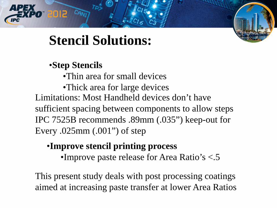
Stencil Solutions: •Step Stencils
•Thin area for small devices •Thick area for large devices
Limitations: Most Handheld devices don’t have sufficient spacing between components to allow steps IPC 7525B recommends .89mm (.035”) keep-out for Every .025mm (.001”) of step
•Improve stencil printing process •Improve paste release for Area Ratio’s <.5
This present study deals with post processing coatings aimed at increasing paste transfer at lower Area Ratios
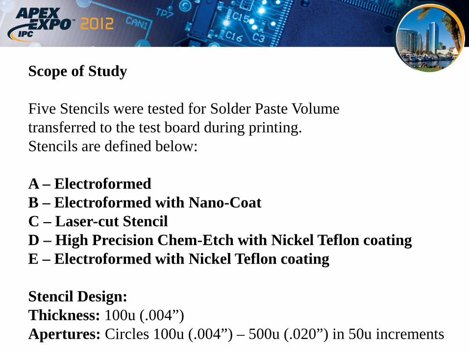
Scope of Study Five Stencils were tested for Solder Paste Volume transferred to the test board during printing. Stencils are defined below: A – Electroformed B – Electroformed with Nano-Coat C – Laser-cut Stencil D – High Precision Chem-Etch with Nickel Teflon coating E – Electroformed with Nickel Teflon coating Stencil Design: Thickness: 100u (.004”) Apertures: Circles 100u (.004”) – 500u (.020”) in 50u increments
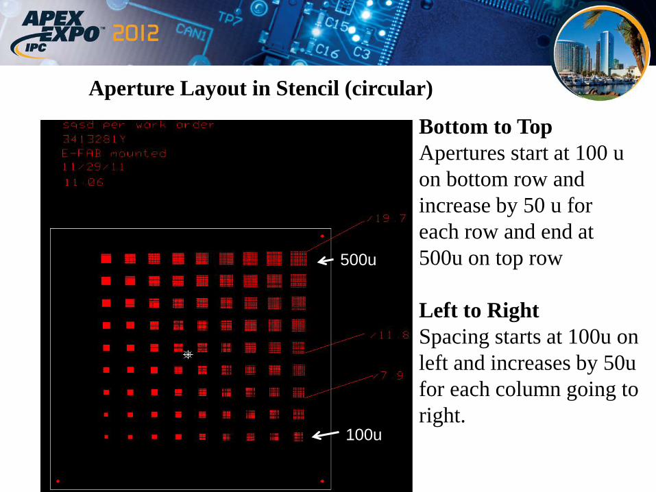
Aperture Layout in Stencil (circular)
Bottom to Top Apertures start at 100 u on bottom row and increase by 50 u for each row and end at 500u on top row Left to Right Spacing starts at 100u on left and increases by 50u for each column going to right.
500u
100u
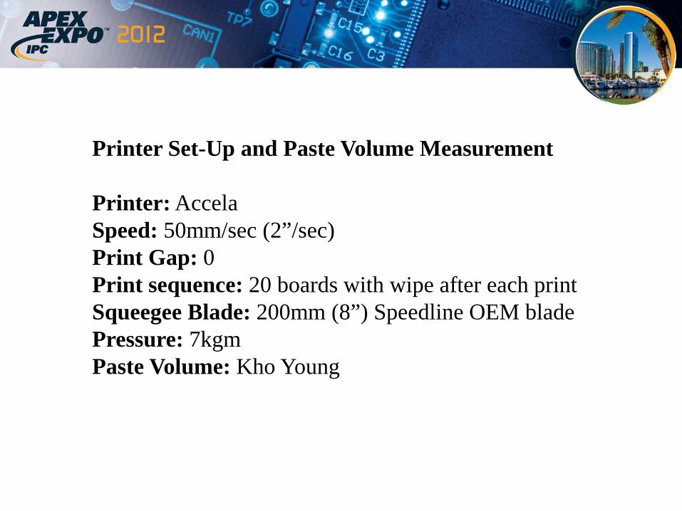
Printer Set-Up and Paste Volume Measurement Printer: Accela Speed: 50mm/sec (2”/sec) Print Gap: 0 Print sequence: 20 boards with wipe after each print Squeegee Blade: 200mm (8”) Speedline OEM blade Pressure: 7kgm Paste Volume: Kho Young
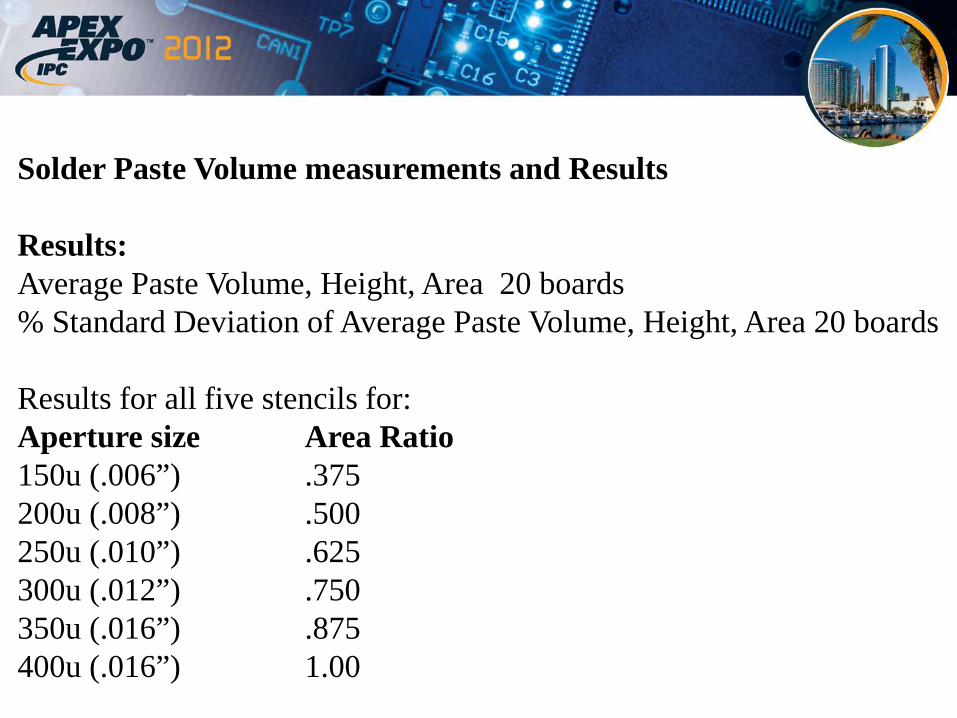
Solder Paste Volume measurements and Results Results: Average Paste Volume, Height, Area 20 boards % Standard Deviation of Average Paste Volume, Height, Area 20 boards Results for all five stencils for: Aperture size Area Ratio 150u (.006”) .375 200u (.008”) .500 250u (.010”) .625 300u (.012”) .750 350u (.016”) .875 400u (.016”) 1.00
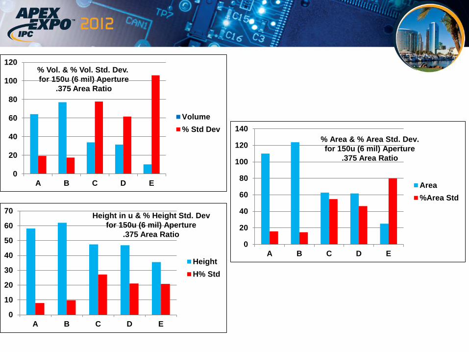
% Vol. & % Vol. Std. Dev. for 150u (6 mil) Aperture
.375 Area Ratio
0
20
40
60
80
100
120
A B C D E
Volume% Std Dev
0
10
20
30
40
50
60
70
A B C D E
HeightH% Std
Height in u & % Height Std. Dev for 150u (6 mil) Aperture
.375 Area Ratio 0
20
40
60
80
100
120
140
A B C D E
Area%Area Std
% Area & % Area Std. Dev. for 150u (6 mil) Aperture
.375 Area Ratio
0102030405060708090
100
A B C D E
Volume% Std Dev
% Vol. & % Vol. Std. Dev. for 200u (8 mil) Aperture
.500 Area Ratio
0
10
20
30
40
50
60
70
80
A B C D E
HeightH% Std
Height in u & % Height Std. Dev for 200u (8 mil) Aperture .500 Area Ratio
0
20
40
60
80
100
120
140
A B C D E
Area%Area Std
% Area & % Area Std. Dev. for 200u (8 mil) Aperture
.500 Area Ratio
0102030405060708090
100
A B C D E
Volume% Std Dev
% Vol. & % Vol. Std. Dev. for 250u (10 mil) Aperture .625 Area Ratio
0102030405060708090
A B C D E
HeightH% Std
Height in u & % Height Std. Dev for 250u (10 mil) Aperture .625 Area Ratio
0
20
40
60
80
100
120
140
A B C D E
Area%Area Std
% Area & % Area Std. Dev. for 250u (10 mil) Aperture
.625 Area Ratio
0102030405060708090
100
A B C D E
Volume% Std Dev
% Vol. & % Vol. Std. Dev. for 300u (12 mil) Aperture .750 Area Ratio
0102030405060708090
A B C D E
HeightH% Std
Height in u & % Height Std. Dev for 300u (12 mil) Aperture .750 Area Ratio
0
20
40
60
80
100
120
140
A B C D E
Area%Area Std
% Area & % Area Std. Dev. for 300u (12 mil) Aperture .750 Area Ratio
0
20
40
60
80
100
120
A B C D E
Volume% Std Dev
% Vol. & % Vol. Std. Dev. for 400u (16 mil) Aperture 1.000 Area Ratio
0102030405060708090
100
A B C D E
HeightH% Std
0
20
40
60
80
100
120
140
A B C D E
Area%Area Std
% Area & % Area Std. Dev. for 400u (16 mil) Aperture1.000 Area Ratio
0.0
20.0
40.0
60.0
80.0
100.0
120.0
150 200 250 300 350 400
ABCDE
% Volume vs. Aperture Size microns
% Volume at each intersection Stencil Aperture
150 200 250 300 350 400 A 64.3 83.5 87.6 90.1 92.4 91.3 B 77.1 88.9 92.5 95.1 97.3 96.6 C 33.9 58.1 69.1 78.5 84.2 85.6 D 31.5 78.2 85.4 86.2 87.1 90.0 E 10.3 73.9 86.7 93.0 98.8 99.5
Area Ratio .375 .500 .675 .750 .875 1.000
0.0
20.0
40.0
60.0
80.0
100.0
120.0
150 200 250 300 350 400
ABCDE
% Volume Standard Deviation vs. Aperture size microns
Volume % Std Dev at each intersection Stencil Aperture
150 200 250 300 350 400 A 19.3 8.8 6.6 6.4 5.3 4.9 B 17.5 8.2 6.1 5.4 4.9 4.4 C 77.8 27.2 13.5 8.5 6.3 5.1 D 61.7 10.1 7.6 5.2 4.1 3.2 E 106.0 17.0 9.3 7.4 6.6 6.0
Area Ratio .375 .500 .675 .750 .875 1.000
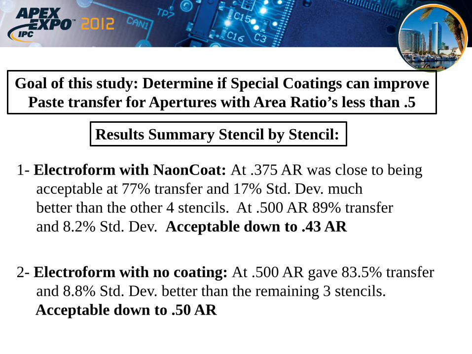
Goal of this study: Determine if Special Coatings can improve Paste transfer for Apertures with Area Ratio’s less than .5
Results Summary Stencil by Stencil:
1- Electroform with NaonCoat: At .375 AR was close to being acceptable at 77% transfer and 17% Std. Dev. much better than the other 4 stencils. At .500 AR 89% transfer and 8.2% Std. Dev. Acceptable down to .43 AR
2- Electroform with no coating: At .500 AR gave 83.5% transfer and 8.8% Std. Dev. better than the remaining 3 stencils. Acceptable down to .50 AR
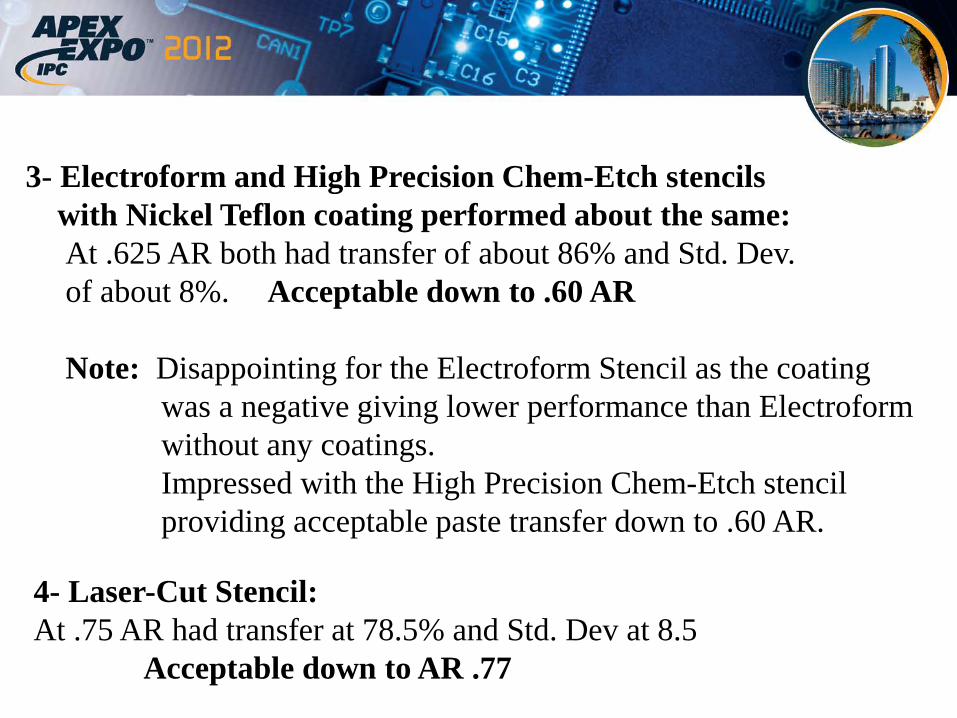
3- Electroform and High Precision Chem-Etch stencils with Nickel Teflon coating performed about the same: At .625 AR both had transfer of about 86% and Std. Dev. of about 8%. Acceptable down to .60 AR Note: Disappointing for the Electroform Stencil as the coating was a negative giving lower performance than Electroform without any coatings. Impressed with the High Precision Chem-Etch stencil providing acceptable paste transfer down to .60 AR.
4- Laser-Cut Stencil: At .75 AR had transfer at 78.5% and Std. Dev at 8.5 Acceptable down to AR .77