specifications subject to change without … · specifications subject to change without notice...
TRANSCRIPT
SPECIFICATIONS SUBJECT TO CHANGE WITHOUT NOTICE
Notice
While reasonable efforts have been made to assure the accuracy of this document, Telit assumes no
liability resulting from any inaccuracies or omissions in this document, or from use of the information
obtained herein. The information in this document has been carefully checked and is believed to be
entirely reliable. However, no responsibility is assumed for inaccuracies or omissions. Telit reserves
the right to make changes to any products described herein and reserves the right to revise this
document and to make changes from time to time in content hereof with no obligation to notify any
person of revisions or changes. Telit does not assume any liability arising out of the application or use
of any product, software, or circuit described herein; neither does it convey license under its patent
rights or the rights of others.
It is possible that this publication may contain references to, or information about Telit products
(machines and programs), programming, or services that are not announced in your country. Such
references or information must not be construed to mean that Telit intends to announce such Telit
products, programming, or services in your country.
Copyrights
This instruction manual and the Telit products described in this instruction manual may be, include or
describe copyrighted Telit material, such as computer programs stored in semiconductor memories or
other media. Laws in the Italy and other countries preserve for Telit and its licensors certain exclusive
rights for copyrighted material, including the exclusive right to copy, reproduce in any form,
distribute and make derivative works of the copyrighted material. Accordingly, any copyrighted
material of Telit and its licensors contained herein or in the Telit products described in this instruction
manual may not be copied, reproduced, distributed, merged or modified in any manner without the
express written permission of Telit. Furthermore, the purchase of Telit products shall not be deemed
to grant either directly or by implication, estoppel, or otherwise, any license under the copyrights,
patents or patent applications of Telit, as arises by operation of law in the sale of a product.
Computer Software Copyrights
The Telit and 3rd Party supplied Software (SW) products described in this instruction manual may
include copyrighted Telit and other 3rd Party supplied computer programs stored in semiconductor
memories or other media. Laws in the Italy and other countries preserve for Telit and other 3rd Party
supplied SW certain exclusive rights for copyrighted computer programs, including the exclusive
right to copy or reproduce in any form the copyrighted computer program. Accordingly, any
copyrighted Telit or other 3rd Party supplied SW computer programs contained in the Telit products
described in this instruction manual may not be copied (reverse engineered) or reproduced in any
manner without the express written permission of Telit or the 3rd Party SW supplier. Furthermore, the
purchase of Telit products shall not be deemed to grant either directly or by implication, estoppel, or
otherwise, any license under the copyrights, patents or patent applications of Telit or other 3rd Party
supplied SW, except for the normal non-exclusive, royalty free license to use that arises by operation
of law in the sale of a product.

Usage and Disclosure Restrictions
License Agreements
The software described in this document is the property of Telit and its licensors. It is furnished by
express license agreement only and may be used only in accordance with the terms of such an
agreement.
Copyrighted Materials
Software and documentation are copyrighted materials. Making unauthorized copies is prohibited by
law. No part of the software or documentation may be reproduced, transmitted, transcribed, stored in a
retrieval system, or translated into any language or computer language, in any form or by any means,
without prior written permission of Telit
High Risk Materials
Components, units, or third-party products used in the product described herein are NOT fault-tolerant
and are NOT designed, manufactured, or intended for use as on-line control equipment in the
following hazardous environments requiring fail-safe controls: the operation of Nuclear Facilities,
Aircraft Navigation or Aircraft Communication Systems, Air Traffic Control, Life Support, or
Weapons Systems (High Risk Activities"). Telit and its supplier(s) specifically disclaim any expressed
or implied warranty of fitness for such High Risk Activities.
Trademarks
TELIT and the Stylized T Logo are registered in Trademark Office. All other product or service
names are the property of their respective owners.
Copyright © Telit Communications S.p.A.
Contents
The aim of this document is the description of typical hardware solutions useful for developing a
product with the Telit UE910 V2 module.
This document is intended for Telit customers who are about to implement their applications using
our UE910 V2 modules.
For general contact, technical support, to report documentation errors and to order manuals, contact
Telit Technical Support Center (TTSC) at:
Alternatively, use:
http://www.telit.com/en/products/technical-support-center/contact.php
For detailed information about where to buy the Telit modules or for recommendations on accessories
and components visit:
http://www.telit.com
To register for product news and announcements or for product questions contact Telit Technical
Support Center (TTSC).
Our aim is to make this guide as helpful as possible. Please keep us informed of comments and
suggestions for improvements.
Telit appreciates feedback from the users of our information.
This document contains the following chapters:
Chapter 1: “Introduction” provides a scope for this document, target audience, contact and support
information, and text conventions.
Chapter 2: “General Product Description” gives an overview of the features of the product.
Chapter 3: “UE910 V2 Module Connections” deals with the pin out configuration and layout.
Chapter 4: “Hardware Commands” How to operate the module via hardware.
Chapter 5: “Power supply” Power supply requirements and general design rules.
Chapter 6: “Antenna” The antenna connection and board layout design are the most important parts in
the full product design.
Chapter 7: “Logic level specification” Specific values adopted in the implementation of logic levels
for this module.
Chapter 8: “USB Port” The USB port on the Telit UE910 V2 is the core of the interface between the
module and OEM hardware.
Chapter 9: “Serial ports” Refers to the serial ports of the Telit UE910 V2.
Chapter 10: “Audio Section” Refers to the audio blocks of the Base Band Chip of the UE910 V2 Telit
Module.
Chapter 11: “General Purpose I/O” How the general purpose I/O pads can be configured.
Chapter 12: “ADC section” Deals with this one kind of converter.
Chapter 13: “Mounting UE910 V2 on the Application” Mechanical dimensions and
recommendations on how to mount the module on the user’s board.
Chapter 14: “Application Design Guide” Deals with the design of host system for download or
upgrade.
Chapter 15: “Safety Recommendation” provides some safety recommendations that must be followed
by the customer in the design of the application that makes use of the Telit UE910 V2.
Chapter 16: “Conformity Assessment Issues” provides some fundamental hints about the conformity
assessment that the final application might need.
Danger – This information MUST be followed or catastrophic equipment failure or bodily injury
may occur.
Caution or Warning – Alerts the user to important points about integrating the module. If these
points are not followed, the module and end user equipment may fail or malfunction.
Tip or Information – Provides advice and suggestions that may be useful when integrating the
module.
All dates are in ISO 8601 format, i.e. YYYY-MM-DD.
Telit UE910 V2 AT Commands Reference Guide : 80419ST10124A
Telit UE910 V2 Software User Guide : 1VV0301066
Telit xE910 Global Form Factor Application Note : 80000NT10060A
Telit xE910 RTC Backup Application Note : 80000NT10072A
Telit UE HE910V2 DE CE910 HE920 DVI Application Note 80000NT10101A
SIM integration design guide : 80000NT10001a
Telit EVK2 User Guide Application Note : 1vv0300704
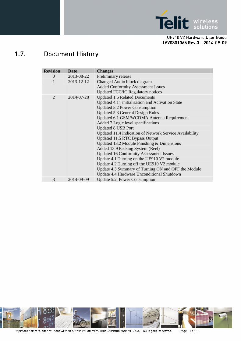
Revision Date Changes
0 2013-08-22 Preliminary release
1 2013-12-12 Changed Audio block diagram
Added Conformity Assessment Issues
Updated FCC/IC Regulatory notices
2 2014-07-28 Updated 1.6 Related Documents
Updated 4.11 initialization and Activation State
Updated 5.2 Power Consumption
Updated 5.3 General Design Rules
Updated 6.1 GSM/WCDMA Antenna Requirement
Added 7 Logic level specifications
Updated 8 USB Port
Updated 11.4 Indication of Network Service Availability
Updated 11.5 RTC Bypass Output
Updated 13.2 Module Finishing & Dimensions
Added 13.9 Packing System (Reel)
Updated 16 Conformity Assessment Issues
Update 4.1 Turning on the UE910 V2 module
Update 4.2 Turning off the UE910 V2 module
Update 4.3 Summary of Turning ON and OFF the Module
Update 4.4 Hardware Unconditional Shutdown
3 2014-09-09 Update 5.2. Power Consumption
The aim of this document is the description of typical hardware solutions useful for developing a
product with the Telit UE910 V2 module.
In this document all the basic functions of a mobile device will be taken into account; for each one of
them a proper hardware solution will be suggested and eventually the wrong solutions and common
errors to be avoided will be evidenced. Obviously this document cannot embrace all hardware
solutions and products that may be designed. Avoiding the discussed wrong solutions must be
considered as mandatory. While the suggested hardware configurations must not be considered
mandatory, the information given must be used as a guide and a starting point for properly developing
a product with the Telit UE910 V2 module.
NOTE:
The integration of the GSM/GPRS/EGPRS/WCDMA/HSDPA UE910 V2 module within a user
application must be done according to the design rules described in this manual.
The information presented in this document is believed to be accurate and reliable. However, no
responsibility is assumed by Telit Communication S.p.A. for its use, such as any infringement of
patents or other rights of third parties. No license is granted by implication or otherwise under any
patent rights of Telit Communication S.p.A. other than for circuitry embodied in Telit products. This
document is subject to change without notice.
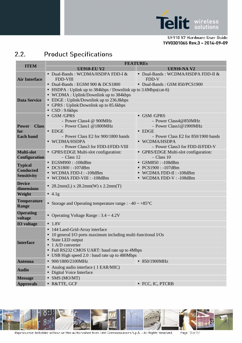
ITEM FEATUREs
UE910-EU V2 UE910-NA V2
Air Interface
Dual-Bands : WCDMA/HSDPA FDD-I &
FDD-VIII
Dual-Bands : EGSM 900 & DCS1800
Dual-Bands : WCDMA/HSDPA FDD-II &
FDD-V
Dual-Bands : GSM 850/PCS1900
Data Service
HSDPA : Uplink up to 384kbps / Downlink up to 3.6Mbps(cat-6)
WCDMA : Uplink/Downlink up to 384kbps
EDGE : Uplink/Downlink up to 236.8kbps
GPRS : Uplink/Downlink up to 85.6kbps
CSD : 9.6kbps
Power Class
for
Each band
GSM /GPRS
- Power Class4 @ 900MHz
- Power Class1 @1800MHz
EDGE
- Power Class E2 for 900/1800 bands
WCDMA/HSDPA
- Power Class3 for FDD-I/FDD-VIII
GSM /GPRS
- Power Class4@850MHz
- Power Class1@1900MHz
EDGE
- Power Class E2 for 850/1900 bands
WCDMA/HSDPA
- Power Class3 for FDD-II/FDD-V
Multi-slot
Configuration
GPRS/EDGE Multi-slot configuration:
- Class 12
GPRS/EDGE Multi-slot configuration:
- Class 10
Typical
Conducted
Sensitivity
EGSM900 : -108dBm
DCS1800 : -107dBm
WCDMA FDD-I : -108dBm
WCDMA FDD-VIII : -108dBm
GSM850 : -108dBm
PCS1900 : -107dBm
WCDMA FDD-II : -108dBm
WCDMA FDD-V : -108dBm
Device
dimensions 28.2mm(L) x 28.2mm(W) x 2.2mm(T)
Weight 4.1g
Temperature
Range Storage and Operating temperature range : –40 ~ +85°C
Operating
voltage Operating Voltage Range : 3.4 ~ 4.2V
IO voltage 1.8V
Interface
144 Land-Grid-Array interface
10 general I/O ports maximum including multi-functional I/Os
State LED output
1 A/D converter
Full RS232 CMOS UART: baud rate up to 4Mbps
USB High speed 2.0 : baud rate up to 480Mbps
Antenna 900/1800/2100MHz 850/1900MHz
Audio Analog audio interface ( 1 EAR/MIC)
Digital Voice Interface
Message SMS (MO/MT)
Approvals R&TTE, GCF FCC, IC, PTCRB

As a part of Telit’s corporate policy of environmental protection, the UE910 V2 complies with the
RoHS (Restriction of Hazardous Substances) directive of the European Union (EU directive
2002/95/EG).
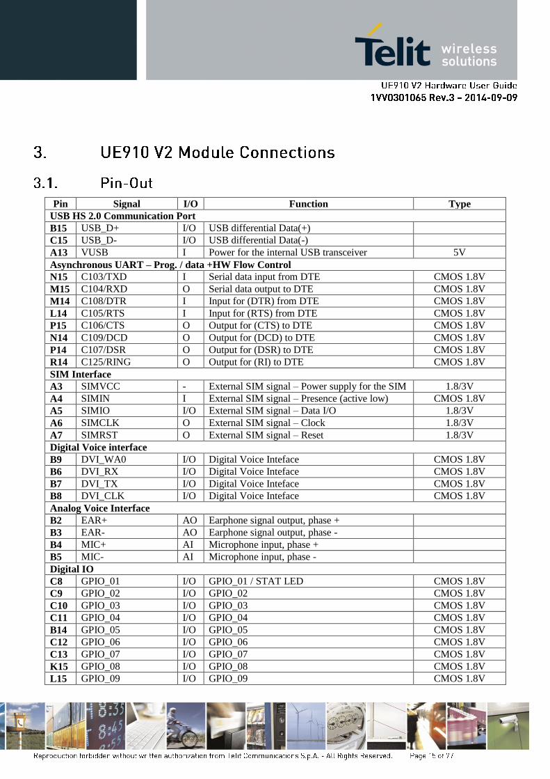
Pin Signal I/O Function Type
USB HS 2.0 Communication Port
B15 USB_D+ I/O USB differential Data(+)
C15 USB_D- I/O USB differential Data(-)
A13 VUSB I Power for the internal USB transceiver 5V
Asynchronous UART – Prog. / data +HW Flow Control
N15 C103/TXD I Serial data input from DTE CMOS 1.8V
M15 C104/RXD O Serial data output to DTE CMOS 1.8V
M14 C108/DTR I Input for (DTR) from DTE CMOS 1.8V
L14 C105/RTS I Input for (RTS) from DTE CMOS 1.8V
P15 C106/CTS O Output for (CTS) to DTE CMOS 1.8V
N14 C109/DCD O Output for (DCD) to DTE CMOS 1.8V
P14 C107/DSR O Output for (DSR) to DTE CMOS 1.8V
R14 C125/RING O Output for (RI) to DTE CMOS 1.8V
SIM Interface
A3 SIMVCC - External SIM signal – Power supply for the SIM 1.8/3V
A4 SIMIN I External SIM signal – Presence (active low) CMOS 1.8V
A5 SIMIO I/O External SIM signal – Data I/O 1.8/3V
A6 SIMCLK O External SIM signal – Clock 1.8/3V
A7 SIMRST O External SIM signal – Reset 1.8/3V
Digital Voice interface
B9 DVI_WA0 I/O Digital Voice Inteface CMOS 1.8V
B6 DVI_RX I/O Digital Voice Inteface CMOS 1.8V
B7 DVI_TX I/O Digital Voice Inteface CMOS 1.8V
B8 DVI_CLK I/O Digital Voice Inteface CMOS 1.8V
Analog Voice Interface
B2 EAR+ AO Earphone signal output, phase +
B3 EAR- AO Earphone signal output, phase -
B4 MIC+ AI Microphone input, phase +
B5 MIC- AI Microphone input, phase -
Digital IO
C8 GPIO_01 I/O GPIO_01 / STAT LED CMOS 1.8V
C9 GPIO_02 I/O GPIO_02 CMOS 1.8V
C10 GPIO_03 I/O GPIO_03 CMOS 1.8V
C11 GPIO_04 I/O GPIO_04 CMOS 1.8V
B14 GPIO_05 I/O GPIO_05 CMOS 1.8V
C12 GPIO_06 I/O GPIO_06 CMOS 1.8V
C13 GPIO_07 I/O GPIO_07 CMOS 1.8V
K15 GPIO_08 I/O GPIO_08 CMOS 1.8V
L15 GPIO_09 I/O GPIO_09 CMOS 1.8V
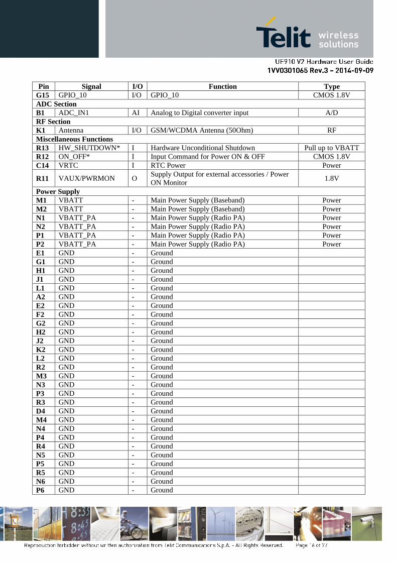
Pin Signal I/O Function Type
G15 GPIO_10 I/O GPIO_10 CMOS 1.8V
ADC Section
B1 ADC_IN1 AI Analog to Digital converter input A/D
RF Section
K1 Antenna I/O GSM/WCDMA Antenna (50Ohm) RF
Miscellaneous Functions
R13 HW_SHUTDOWN* I Hardware Unconditional Shutdown Pull up to VBATT
R12 ON_OFF* I Input Command for Power ON & OFF CMOS 1.8V
C14 VRTC I RTC Power Power
R11 VAUX/PWRMON O Supply Output for external accessories / Power
ON Monitor 1.8V
Power Supply
M1 VBATT - Main Power Supply (Baseband) Power
M2 VBATT - Main Power Supply (Baseband) Power
N1 VBATT_PA - Main Power Supply (Radio PA) Power
N2 VBATT_PA - Main Power Supply (Radio PA) Power
P1 VBATT_PA - Main Power Supply (Radio PA) Power
P2 VBATT_PA - Main Power Supply (Radio PA) Power
E1 GND - Ground
G1 GND - Ground
H1 GND - Ground
J1 GND - Ground
L1 GND - Ground
A2 GND - Ground
E2 GND - Ground
F2 GND - Ground
G2 GND - Ground
H2 GND - Ground
J2 GND - Ground
K2 GND - Ground
L2 GND - Ground
R2 GND - Ground
M3 GND - Ground
N3 GND - Ground
P3 GND - Ground
R3 GND - Ground
D4 GND - Ground
M4 GND - Ground
N4 GND - Ground
P4 GND - Ground
R4 GND - Ground
N5 GND - Ground
P5 GND - Ground
R5 GND - Ground
N6 GND - Ground
P6 GND - Ground
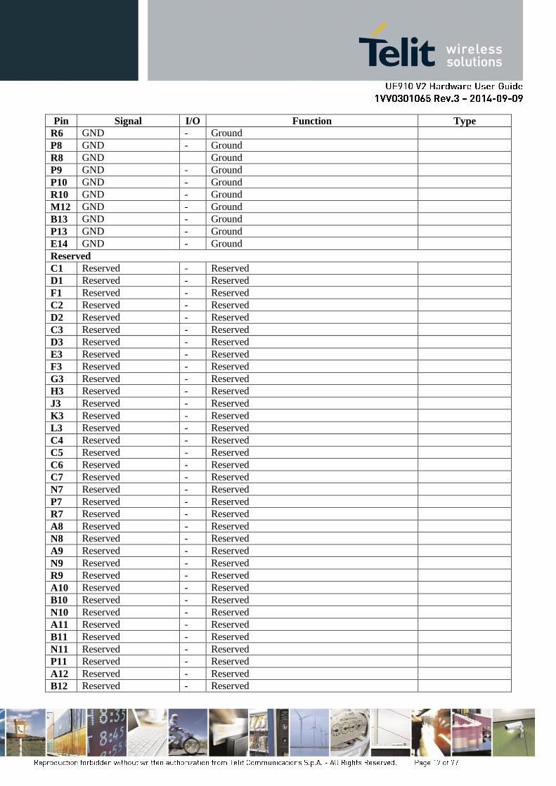
Pin Signal I/O Function Type
R6 GND - Ground
P8 GND - Ground
R8 GND Ground
P9 GND - Ground
P10 GND - Ground
R10 GND - Ground
M12 GND - Ground
B13 GND - Ground
P13 GND - Ground
E14 GND - Ground
Reserved
C1 Reserved - Reserved
D1 Reserved - Reserved
F1 Reserved - Reserved
C2 Reserved - Reserved
D2 Reserved - Reserved
C3 Reserved - Reserved
D3 Reserved - Reserved
E3 Reserved - Reserved
F3 Reserved - Reserved
G3 Reserved - Reserved
H3 Reserved - Reserved
J3 Reserved - Reserved
K3 Reserved - Reserved
L3 Reserved - Reserved
C4 Reserved - Reserved
C5 Reserved - Reserved
C6 Reserved - Reserved
C7 Reserved - Reserved
N7 Reserved - Reserved
P7 Reserved - Reserved
R7 Reserved - Reserved
A8 Reserved - Reserved
N8 Reserved - Reserved
A9 Reserved - Reserved
N9 Reserved - Reserved
R9 Reserved - Reserved
A10 Reserved - Reserved
B10 Reserved - Reserved
N10 Reserved - Reserved
A11 Reserved - Reserved
B11 Reserved - Reserved
N11 Reserved - Reserved
P11 Reserved - Reserved
A12 Reserved - Reserved
B12 Reserved - Reserved
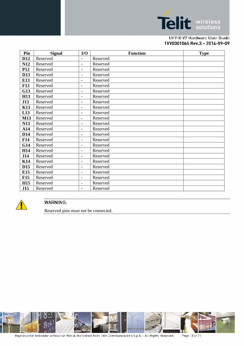
Pin Signal I/O Function Type
D12 Reserved - Reserved
N12 Reserved - Reserved
P12 Reserved - Reserved
D13 Reserved - Reserved
E13 Reserved - Reserved
F13 Reserved - Reserved
G13 Reserved - Reserved
H13 Reserved - Reserved
J13 Reserved - Reserved
K13 Reserved - Reserved
L13 Reserved - Reserved
M13 Reserved - Reserved
N13 Reserved - Reserved
A14 Reserved - Reserved
D14 Reserved - Reserved
F14 Reserved - Reserved
G14 Reserved - Reserved
H14 Reserved - Reserved
J14 Reserved - Reserved
K14 Reserved - Reserved
D15 Reserved - Reserved
E15 Reserved - Reserved
F15 Reserved - Reserved
H15 Reserved - Reserved
J15 Reserved - Reserved
Reserved pins must not be connected
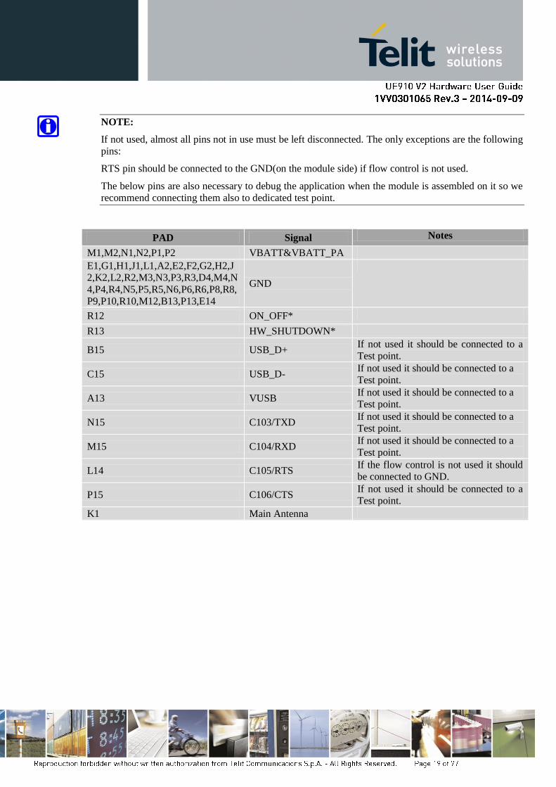
NOTE:
If not used, almost all pins not in use must be left disconnected. The only exceptions are the following
pins:
RTS pin should be connected to the GND(on the module side) if flow control is not used.
The below pins are also necessary to debug the application when the module is assembled on it so we
recommend connecting them also to dedicated test point.
PAD Signal Notes
M1,M2,N1,N2,P1,P2 VBATT&VBATT_PA
E1,G1,H1,J1,L1,A2,E2,F2,G2,H2,J
2,K2,L2,R2,M3,N3,P3,R3,D4,M4,N
4,P4,R4,N5,P5,R5,N6,P6,R6,P8,R8,
P9,P10,R10,M12,B13,P13,E14
GND
R12 ON_OFF*
R13 HW_SHUTDOWN*
B15 USB_D+ If not used it should be connected to a
Test point.
C15 USB_D- If not used it should be connected to a
Test point.
A13 VUSB If not used it should be connected to a
Test point.
N15 C103/TXD If not used it should be connected to a
Test point.
M15 C104/RXD If not used it should be connected to a
Test point.
L14 C105/RTS If the flow control is not used it should
be connected to GND.
P15 C106/CTS If not used it should be connected to a
Test point.
K1 Main Antenna
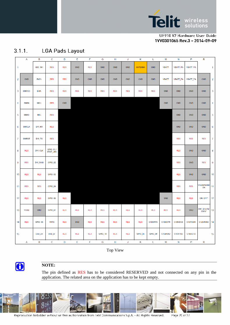
Top View
NOTE:
The pin defined as RES has to be considered RESERVED and not connected on any pin in the
application. The related area on the application has to be kept empty.
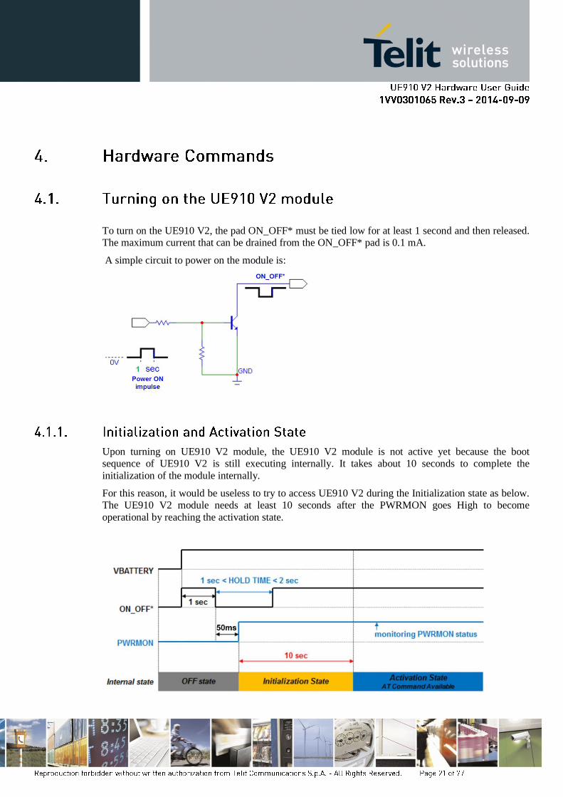
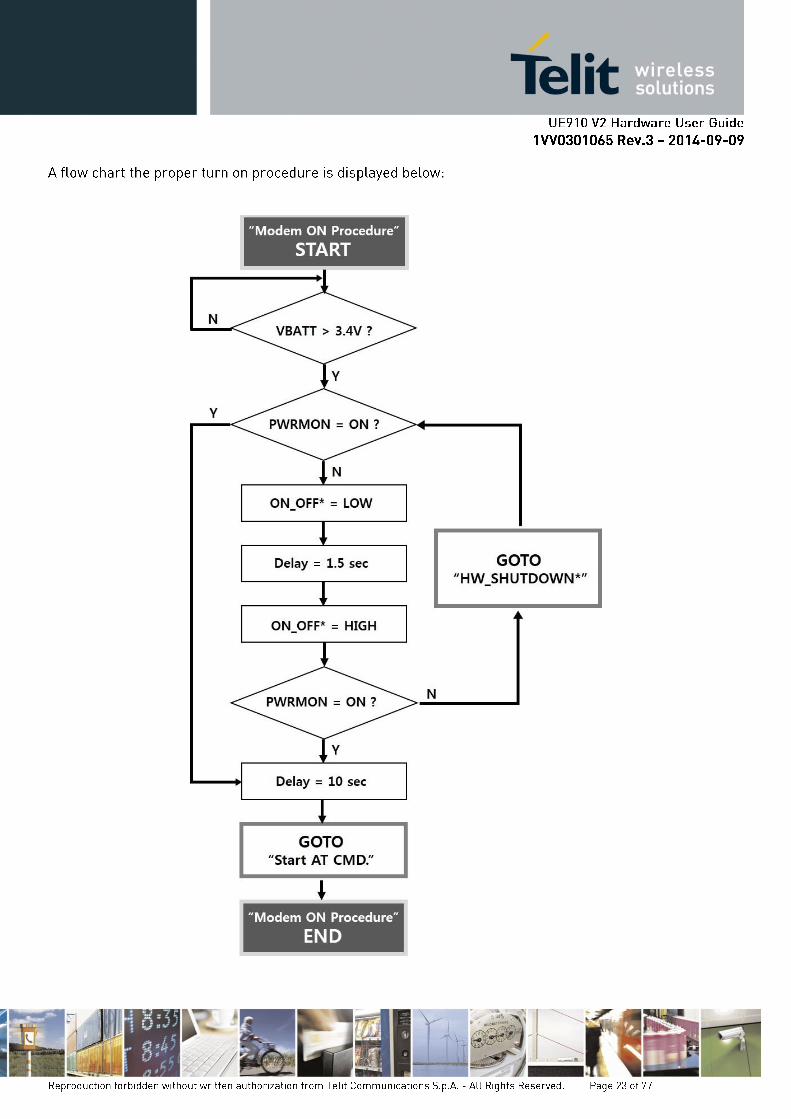
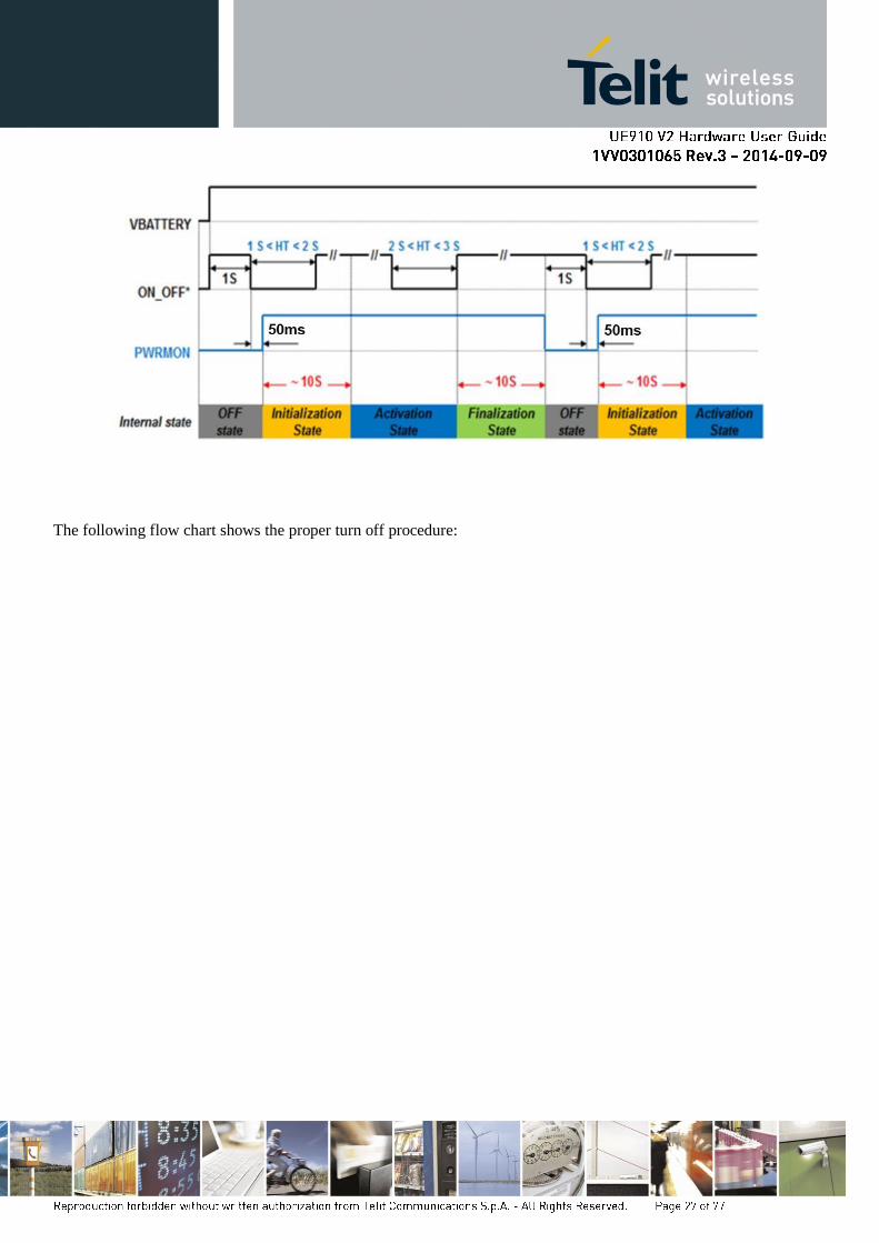
To turn on the UE910 V2, the pad ON_OFF* must be tied low for at least 1 second and then released.
The maximum current that can be drained from the ON_OFF* pad is 0.1 mA.
A simple circuit to power on the module is:
Upon turning on UE910 V2 module, the UE910 V2 module is not active yet because the boot
sequence of UE910 V2 is still executing internally. It takes about 10 seconds to complete the
initialization of the module internally.
For this reason, it would be useless to try to access UE910 V2 during the Initialization state as below.
The UE910 V2 module needs at least 10 seconds after the PWRMON goes High to become
operational by reaching the activation state.
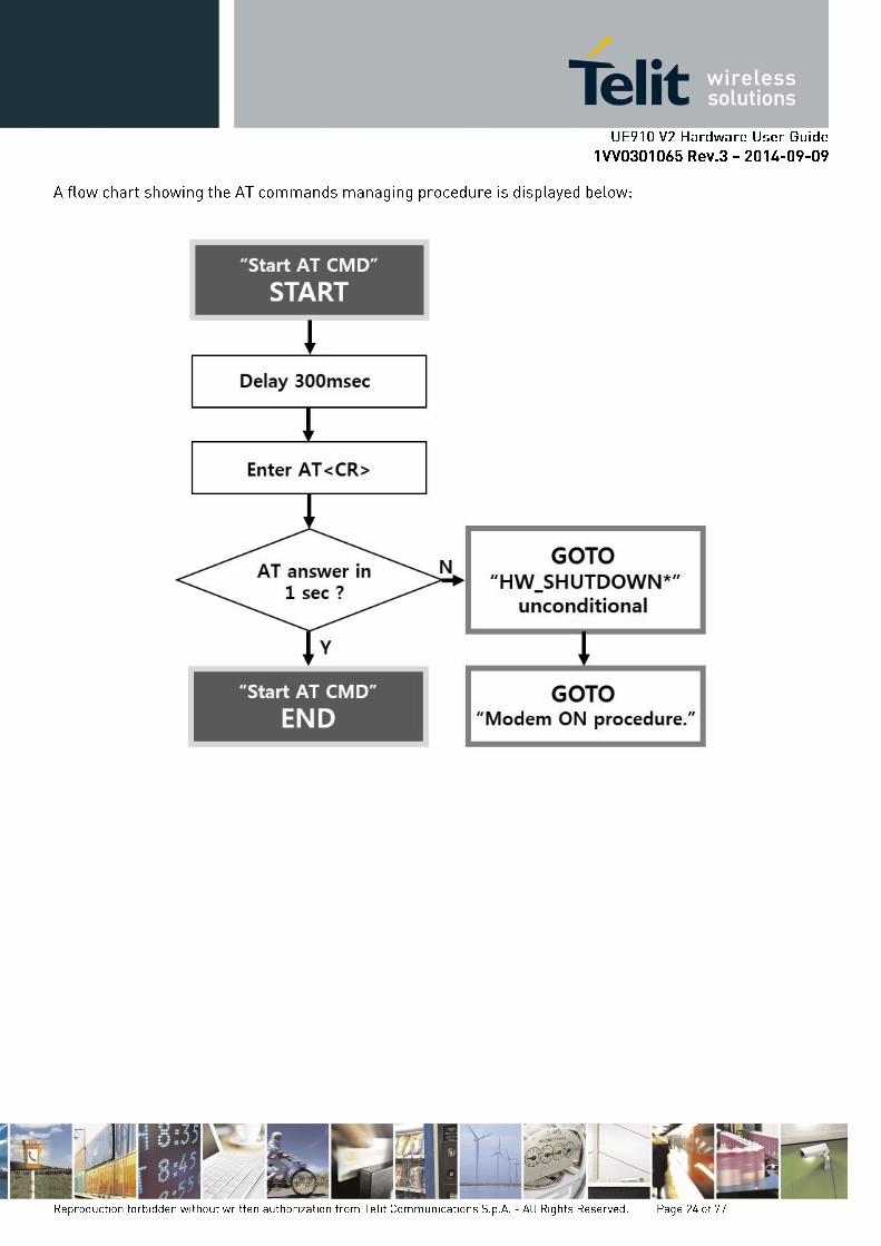
During the Initialization state, any kind of AT-command is not available. DTE must wait for the
Activation state to communicate with UE910 V2.
To check if the UE910 V2 has powered on, the hardware line VAUX/PWRMON must be monitored.
When VAUX/PWRMON goes high, the module has powered on.
NOTE:
Do not use any pull up resistor on the ON_OFF* line. It is pulled up with 250kΩ internally. Using a
pull up resistor may bring latch up problems on the UE910 V2 power regulator and improper power
on/off of the module. The line ON_OFF* must be connected only in open collector configuration.
NOTE:
In this document all the lines are inverted. Active low signals are labeled with a name that ends with
"*" or with a bar over the name.
NOTE:
In order to avoid a back powering effect it is recommended to avoid having any HIGH logic level
signal applied to the digital pins of the UE910 V2 module when the module is powered OFF or during
an ON/OFF transition.
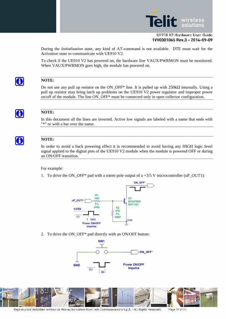
For example:
1. To drive the ON_OFF* pad with a totem pole output of a +3/5 V microcontroller (uP_OUT1):
2. To drive the ON_OFF* pad directly with an ON/OFF button:
Turning off the device can be done in two ways:
via AT command (see UE910 V2 Software User Guide, AT#SHDN)
by tying low pin ON_OFF*
Either ways, the device issues a detach request to network informing that the device will not be
reachable any more.
To turn OFF the UE910 V2 the pad ON_OFF* must be tied low for at least 2 seconds and then
released.
TIP:
To check if the device has powered off, hardware line PWRMON must be monitored.
The device is powered off when PWRMON goes low.
NOTE:
In order to avoid a back powering effect it is recommended to avoid having any HIGH logic level
signal applied to the digital pins of the UE910 V2 when the module is powered OFF or during an
ON/OFF transition.
The UE910 V2 can be shut down by a software command.
When a shutdown command is sent, the UE910 V2 goes into the finalization state and will shut down
PWRMON at the end of this state. The period of the finalization state can vary according to the state
of the UE910 V2 so it cannot be fixed definitely.
Normally it will be 10 seconds after sending a shutdown command and DTE should monitor the status
of PWRMON to see the actual power off.
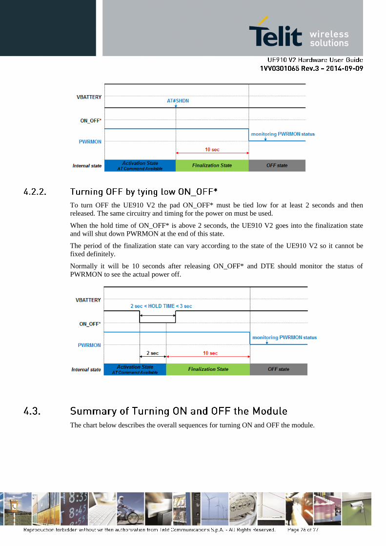
To turn OFF the UE910 V2 the pad ON_OFF* must be tied low for at least 2 seconds and then
released. The same circuitry and timing for the power on must be used.
When the hold time of ON_OFF* is above 2 seconds, the UE910 V2 goes into the finalization state
and will shut down PWRMON at the end of this state.
The period of the finalization state can vary according to the state of the UE910 V2 so it cannot be
fixed definitely.
Normally it will be 10 seconds after releasing ON_OFF* and DTE should monitor the status of
PWRMON to see the actual power off.
The chart below describes the overall sequences for turning ON and OFF the module.
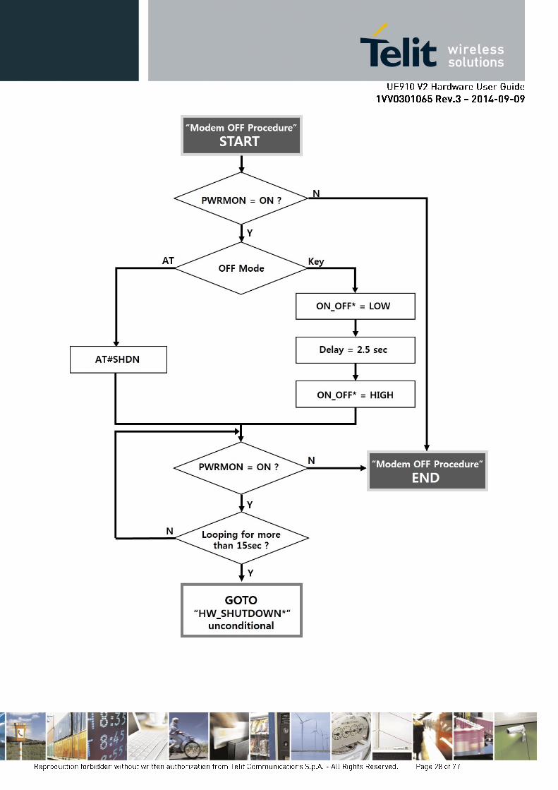
The following flow chart shows the proper turn off procedure:
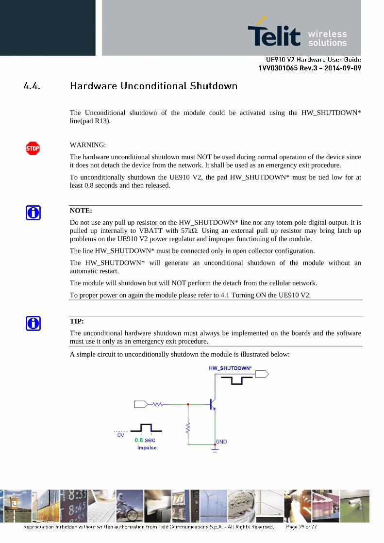
The Unconditional shutdown of the module could be activated using the HW_SHUTDOWN*
line(pad R13).
WARNING:
The hardware unconditional shutdown must NOT be used during normal operation of the device since
it does not detach the device from the network. It shall be used as an emergency exit procedure.
To unconditionally shutdown the UE910 V2, the pad HW_SHUTDOWN* must be tied low for at
least 0.8 seconds and then released.
NOTE:
Do not use any pull up resistor on the HW_SHUTDOWN* line nor any totem pole digital output. It is
pulled up internally to VBATT with 57kΩ. Using an external pull up resistor may bring latch up
problems on the UE910 V2 power regulator and improper functioning of the module.
The line HW_SHUTDOWN* must be connected only in open collector configuration.
The HW_SHUTDOWN* will generate an unconditional shutdown of the module without an
automatic restart.
The module will shutdown but will NOT perform the detach from the cellular network.
To proper power on again the module please refer to 4.1 Turning ON the UE910 V2.
TIP:
The unconditional hardware shutdown must always be implemented on the boards and the software
must use it only as an emergency exit procedure.
A simple circuit to unconditionally shutdown the module is illustrated below:
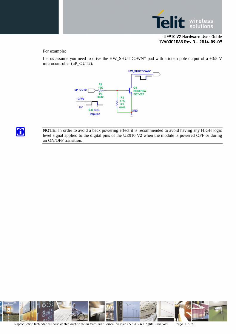
For example:
Let us assume you need to drive the HW_SHUTDOWN* pad with a totem pole output of a +3/5 V
microcontroller (uP_OUT2):
NOTE: In order to avoid a back powering effect it is recommended to avoid having any HIGH logic
level signal applied to the digital pins of the UE910 V2 when the module is powered OFF or during
an ON/OFF transition.
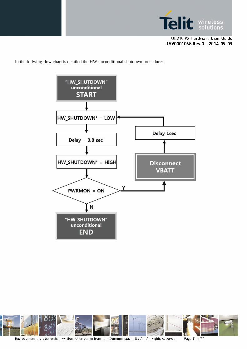
In the follwing flow chart is detailed the HW unconditional shutdown procedure:
The power supply circuitry and board layout are a very important part in the full product design and
they strongly reflect on the product’s overall performance. Read carefully the requirements and the
guidelines that follow for a proper design.
The external power supply must be connected to VBATT & VBATT_PA signals and must fulfill the
following requirements:
Power Supply
Nominal Supply Voltage 3.8V
Normal Operating Voltage range 3.4V ~ 4.2V
Extended Operating Voltage range 3.4V ~ 4.5V
NOTE:
The Operating Voltage Range MUST never be exceeded. Special care must be taken when designing
the application’s power supply section to avoid having an excessive voltage drop.
If the voltage drop is exceeding the limits it could cause a Power Off of the module..
Behavior in the extended operating voltage range might deviate from 3GPP specification.
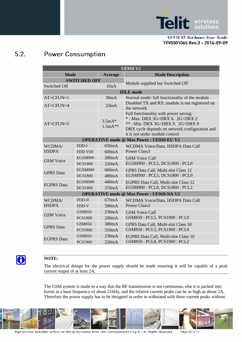
UE910 V2
Mode Average Mode Description
SWITCHED OFF Module supplied but Switched Off
Switched Off 10uA
IDLE mode
AT+CFUN=1 30mA Normal mode: full functionality of the module
AT+CFUN=4 23mA Disabled TX and RX: module is not registered on
the network
AT+CFUN=5 3.5mA*
1.5mA**
Full functionality with power saving:
* : Max. DRX 3G=DRX 6. 2G=DRX 2
** : Min. DRX 3G=DRX 9. 2G=DRX 9
DRX cycle depends on network configuration and
it is not under module control.
OPERATIVE mode @ Max Power : UE910-EU V2
WCDMA/
HSDPA
FDD-I 650mA WCDMA Voice/Data, HSDPA Data Call
Power Class3 FDD-VIII 600mA
GSM Voice EGSM900 280mA GSM Voice Call
EGSM900 : PCL5, DCS1800 : PCL0 DCS1800 220mA
GPRS Data EGSM900 660mA GPRS Data Call, Multi-slot Class 12
EGSM900 : PCL5, DCS1800 : PCL0 DCS1800 480mA
EGPRS Data EGSM900 440mA EGPRS Data Call, Multi-slot Class 12
EGSM900 : PCL8, DCS1800 : PCL2 DCS1800 370mA
OPERATIVE mode @ Max Power : UE910-NA V2
WCDMA/
HSDPA
FDD-II 670mA WCDMA Voice/Data, HSDPA Data Call
Power Class3 FDD-V 590mA
GSM Voice GSM850 230mA GSM Voice Call
GSM850 : PCL5, PCS1900 : PCL0 PCS1900 200mA
GPRS Data GSM850 380mA GPRS Data Call, Multi-slot Class 10
GSM850 : PCL5, PCS1900 : PCL0 PCS1900 310mA
EGPRS Data GSM850 230mA EGPRS Data Call, Multi-slot Class 10
GSM850 : PCL8, PCS1900 : PCL2 PCS1900 220mA
NOTE:
The electrical design for the power supply should be made ensuring it will be capable of a peak
current output of at least 2A.
The GSM system is made in a way that the RF transmission is not continuous, else it is packed into
bursts at a base frequency of about 216Hz, and the relative current peaks can be as high as about 2A.
Therefore the power supply has to be designed in order to withstand with these current peaks without

big voltage drops; this means that both the electrical design and the board layout must be designed for
this current flow. If the layout of the PCB is not well designed a strong noise floor is generated on the
ground and the supply; this will reflect on all the audio paths producing an audible annoying noise at
216Hz; if the voltage drop during the peak current absorption is too much, then the device may even
shutdown as a consequence of the supply voltage drop.
The principal guidelines for the Power Supply Design embrace three different design steps:
the electrical design
the thermal design
the PCB layout
The electrical design of the power supply depends strongly on the power source where this power is
drained. We will distinguish them into three categories:
+5V input (typically PC internal regulator output)
+12V input (typically automotive)
Battery
The desired output for the power supply is 3.8V, hence there is not a big difference
between the input source and the desired output so a linear regulator can be used and it
should withstand with 2A peak current load represented by UE910 V2. A switching
power supply will not be suitable because of the low drop-out requirements.
When using a linear regulator, a proper heat sink must be provided in order to dissipate the
power generated.
A Bypass low ESR capacitor of adequate capacity must be provided in order to cut the
current absorption peaks close to the UE910 V2. A tantalum 100μF capacitor is usually
suited.
Make sure the low ESR capacitor on the power supply output (usually a tantalum one) is
rated at least 10V.
A protection diode should be inserted close to the power input in order to save the UE910
V2 from power polarity inversion.
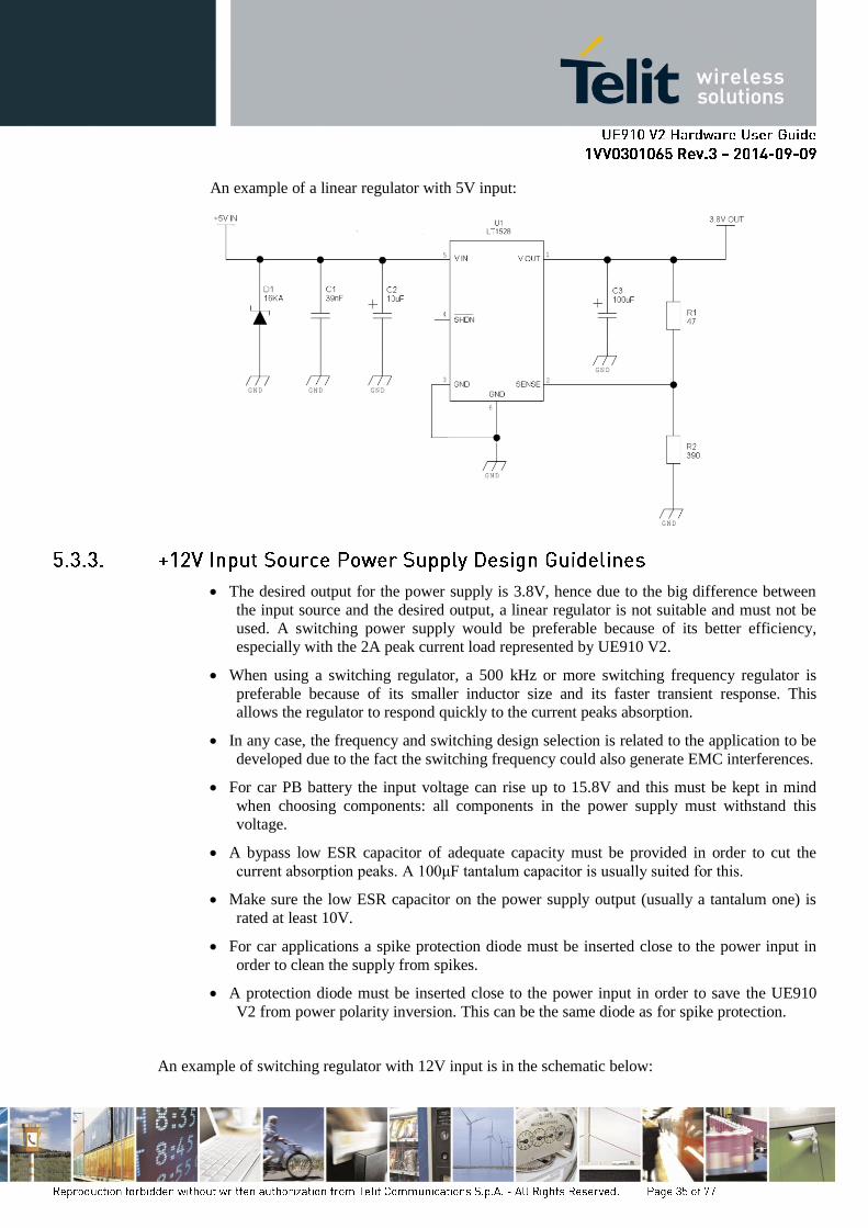
An example of a linear regulator with 5V input:
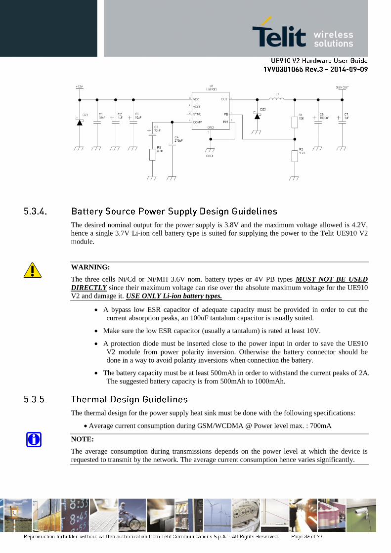
The desired output for the power supply is 3.8V, hence due to the big difference between
the input source and the desired output, a linear regulator is not suitable and must not be
used. A switching power supply would be preferable because of its better efficiency,
especially with the 2A peak current load represented by UE910 V2.
When using a switching regulator, a 500 kHz or more switching frequency regulator is
preferable because of its smaller inductor size and its faster transient response. This
allows the regulator to respond quickly to the current peaks absorption.
In any case, the frequency and switching design selection is related to the application to be
developed due to the fact the switching frequency could also generate EMC interferences.
For car PB battery the input voltage can rise up to 15.8V and this must be kept in mind
when choosing components: all components in the power supply must withstand this
voltage.
A bypass low ESR capacitor of adequate capacity must be provided in order to cut the
current absorption peaks. A 100μF tantalum capacitor is usually suited for this.
Make sure the low ESR capacitor on the power supply output (usually a tantalum one) is
rated at least 10V.
For car applications a spike protection diode must be inserted close to the power input in
order to clean the supply from spikes.
A protection diode must be inserted close to the power input in order to save the UE910
V2 from power polarity inversion. This can be the same diode as for spike protection.
An example of switching regulator with 12V input is in the schematic below:
The desired nominal output for the power supply is 3.8V and the maximum voltage allowed is 4.2V,
hence a single 3.7V Li-ion cell battery type is suited for supplying the power to the Telit UE910 V2
module.
WARNING:
The three cells Ni/Cd or Ni/MH 3.6V nom. battery types or 4V PB types MUST NOT BE USED
DIRECTLY since their maximum voltage can rise over the absolute maximum voltage for the UE910
V2 and damage it. USE ONLY Li-ion battery types.
A bypass low ESR capacitor of adequate capacity must be provided in order to cut the
current absorption peaks, an 100uF tantalum capacitor is usually suited.
Make sure the low ESR capacitor (usually a tantalum) is rated at least 10V.
A protection diode must be inserted close to the power input in order to save the UE910
V2 module from power polarity inversion. Otherwise the battery connector should be
done in a way to avoid polarity inversions when connection the battery.
The battery capacity must be at least 500mAh in order to withstand the current peaks of 2A.
The suggested battery capacity is from 500mAh to 1000mAh.
The thermal design for the power supply heat sink must be done with the following specifications:
Average current consumption during GSM/WCDMA @ Power level max. : 700mA
NOTE:
The average consumption during transmissions depends on the power level at which the device is
requested to transmit by the network. The average current consumption hence varies significantly.

Considering the very low current during idle, especially if the Power Saving function is enabled, it is
possible to consider from the thermal point of view that the device absorbs current significantly only
during calls.
If we assume that the device stays in transmission for short periods of time (let’s say a few minutes)
and then remains for a quite long time in idle (let’s say one hour), then the power supply has always
the time to cool down between the calls and the heat sink could be smaller than the calculated one for
700mA maximum RMS current, or even could be the simple chip package (no heat sink).
Moreover in average network conditions the device is requested to transmit at a lower power level
than the maximum and hence the current consumption will be less than 700mA (usually around 200
mA).
For these reasons the thermal design is rarely a concern and the simple ground plane where the power
supply chip is placed can be enough to ensure a good thermal condition and avoid overheating.
For the heat generated by the UE910 V2, you can consider it to be during transmission 1W max
during CSD/VOICE calls and 2W max during GPRS upload.
This generated heat will be mostly conducted to the ground plane under the UE910 V2; you must
ensure that your application can dissipate it.
As seen on the electrical design guidelines the power supply must have a low ESR capacitor on the
output to cut the current peaks and a protection diode on the input to protect the supply from spikes
and polarity inversion. The placement of these components is crucial for the correct operation of the
circuitry. A misplaced component can be useless or can even decrease the power supply
performances.
The bypass low ESR capacitor must be placed close to the Telit UE910 V2 power input
pads, or in the case the power supply is a switching type it can be placed close to the
inductor to cut the ripple provided the PCB trace from the capacitor to UE910 V2 is wide
enough to ensure a drop-less connection even during the 2A current peaks.
The protection diode must be placed close to the input connector where the power source is
drained.
The PCB traces from the input connector to the power regulator IC must be wide enough
to ensure no voltage drops occur when the 2A current peaks are absorbed.
Note that this is not made in order to save power loss but especially to avoid the voltage
drops on the power line at the current peaks frequently of 216Hz that will reflect on all
the components connected to that supply, introducing the noise floor at the burst base
frequency. For this reason while a voltage drop of 300 – 400mV may be acceptable from
the power loss point of view, the same voltage drop may not be acceptable from the noise
point of view. If your application doesn’t have audio interface but only uses the data
feature of the Telit UE910 V2, then this noise is not so disturbing and power supply
layout design can be more forgiving.
The PCB traces to UE910 V2 and the Bypass capacitor must be wide enough to ensure no
significant voltage drops occur when the 2A current peaks are absorbed. This is for the
same reason as previous point. Try to keep this trace as short as possible.
The PCB traces connecting the switching output to the inductor and the switching diode
must be kept as short as possible by placing the inductor and the diode very close to the
power switching IC (only for switching power supply). This is done in order to reduce the
radiated field (noise) at the switching frequency (usually 100-500 kHz).
The use of a good common ground plane is suggested.
The placement of the power supply on the board should be done in such a way to guarantee
that the high current return paths in the ground plane are not overlapped to any noise
sensitive circuitry such as the microphone amplifier/buffer or earphone amplifier.
The power supply input cables must be kept separate from noise sensitive lines such as
microphone/earphone cables.
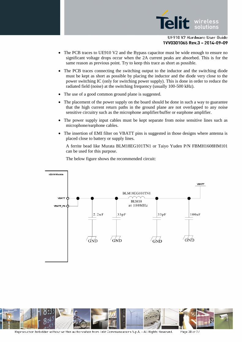
The insertion of EMI filter on VBATT pins is suggested in those designs where antenna is
placed close to battery or supply lines.
A ferrite bead like Murata BLM18EG101TN1 or Taiyo Yuden P/N FBMH1608HM101
can be used for this purpose.
The below figure shows the recommended circuit:
The antenna connection and board layout design are the most important parts in the full product
design and they strongly reflect on the product’s overall performance. Read carefully and follow the
requirements and the guidelines for a proper design.
The antenna for a Telit UE910 V2 device must fulfill the following requirements:
When using the Telit UE910 V2, since there’s no antenna connector on the module, the antenna must
be connected to the UE910 V2 antenna pad (K1) by means of a transmission line implemented in the
PCB.
In the case that the antenna is not directly connected at the antenna pad of the UE910 V2, then a PCB
line is needed in order to connect with it or with its connector.
The transmissions line shall fulfil the following requirements:
Antenna Line on PCB Requirements
Characteristic Impedance 50Ohm
Max Attenuation 0.3dB
Coupling with other signals shall be avoided
Cold End (Ground Plane) of antenna shall be equipotential to the UE910 V2 ground pads
GSM / WCDMA Antenna Requirements
Frequency
range
Depending on the frequency band(s) provided by the network operator, the
customer must use the most suitable antenna for that/those band(s)
Bandwidth
UE910-EU V2 UE910-NA V2
EGSM900 : 80 MHz
DCS1800 : 170 MHz
WCDMA FDD-I : 250 MHz
WCDMA FDD-VIII : 80 MHz
GSM850 : 70 MHz
PCS1900 : 140 MHz
WCDMA FDD-II : 140 MHz
WCDMA FDD-V : 70 MHz
Impedance 50 Ohm
Input power > 33dBm(2W) peak power in GSM
> 24dBm average power in WCDMA
VSWR
absolute max
<= 5:1(limit to avoid permanent damage)
VSWR
recommended
<= 2:1(limit to fulfill all regulatory requirements)
Furthermore if the device is developed for the US market and/or Canada market, it shall comply with
the FCC and/or IC approval requirements:
This device is to be used only for mobile and fixed application. In order to re-use the Telit FCC/IC
approvals the antenna(s) used for this transmitter must be installed to provide a separation distance of
at least 20 cm from all persons and must not be co-located or operating in conjunction with any other
antenna or transmitter then additional FCC/IC testing may be required. End-Users must be provided
with transmitter operation conditions for satisfying RF exposure compliance.
Antennas used for this OEM module must not exceed the gains for mobile and fixed operating
configurations as described in “FCC/IC Regulatory notices” chapter.
Make sure that the transmission line’s characteristic impedance is 50ohm.
Keep line on the PCB as short as possible since the antenna line loss shall be less than around
0.3dB.
Line geometry should have uniform characteristics, constant cross section, avoid meanders and
abrupt curves.
Any kind of suitable geometry/structure can be used for implementing the printed transmission
line afferent the antenna.
If a Ground plane is required in line geometry, that plane has to be continuous and sufficiently
extended so the geometry can be as similar as possible to the related canonical model.
Keep, if possible, at least one layer of the PCB used only for the Ground plane; If possible, use
this layer as reference Ground plane for the transmission line.
It is wise to surround (on both sides) the PCB transmission line with Ground. Avoid having other
signal tracks facing directly the antenna line track.
Avoid crossing any un-shielded transmission line footprint with other tracks on different layers.
The ground surrounding the antenna line on PCB has to be strictly connected to the main Ground
plane by means of via holes (once per 2mm at least) placed close to the ground edges facing
line track.
Place EM noisy devices as far as possible from UE910 V2 antenna line.
Keep the antenna line far away from the UE910 V2 power supply lines.
If EM noisy devices are present on the PCB hosting the UE910 V2, such as fast switching ICs,
take care of shielding them with a metal frame cover.
If EM noisy devices are not present around the line use of geometries like Micro strip or Grounded
Coplanar Waveguide are preferred since they typically ensure less attenuation when compared
to a Strip line having same length.
Install the antenna in a place covered by the GSM/WCDMA signal.
If the device antenna is located greater than 20cm from the human body and there are no co-
located transmitter then the Telit FCC/IC approvals can be re-used by the end product.
If the device antenna is located less than 20cm from the human body or there are co-located
transmitter then the additional FCC/IC testing may be required for the end product.
(Telit FCC/IC approvals cannot be resued.)
Antenna shall not be installed inside the metal cases.
Antenna shall be installed also according to antenna manufacture instructions.
WARNING:
Consider a mechanical design and a low-capacitance ESD protection device to protect UE910 V2 or
customer specific requirements from ESD event to Antenna port (K1).
The following table shows the logic level specifications used in the UE910 V2 interface circuits:
Absolute Maximum Ratings -Not Functional
Parameter Min Max
Input level on any digital pin (CMOS 1.8) with respect to ground -0.3V 2.3V
Operating Range - Interface levels (1.8V CMOS)
Parameter Min Max
Input high level 1.5V 2.1V
Input low level 0.0V 0.35V
Output high level 1.35V 1.8V
Output low level 0.0V 0.45V
Current characteristics
Parameter Typical
Output Current 2mA
Input Current 30uA
The UE910 V2 includes one integrated universal serial bus (USB 2.0 HS) transceiver.
This port is compliant with the USB 2.0 High-speed specification.
The following table is listing the available signals:
Pin Signal I/O Function Note
B15 USB_D+ I/O USB differential Data(+)
C15 USB_D- I/O USB differential Data(-)
A13 VUSB I Power for the internal USB transceiver Acceptable range:
4.4V ~ 5.25V
The USB_DPLUS and USB_DMINUS signals have a clock rate of 480MHz.
The signal traces should be routed carefully. Trace lengths, number of vias and capacitive loading
should be minimized. The characteristic impedance value should be as close as possible to 90ohm
differential.
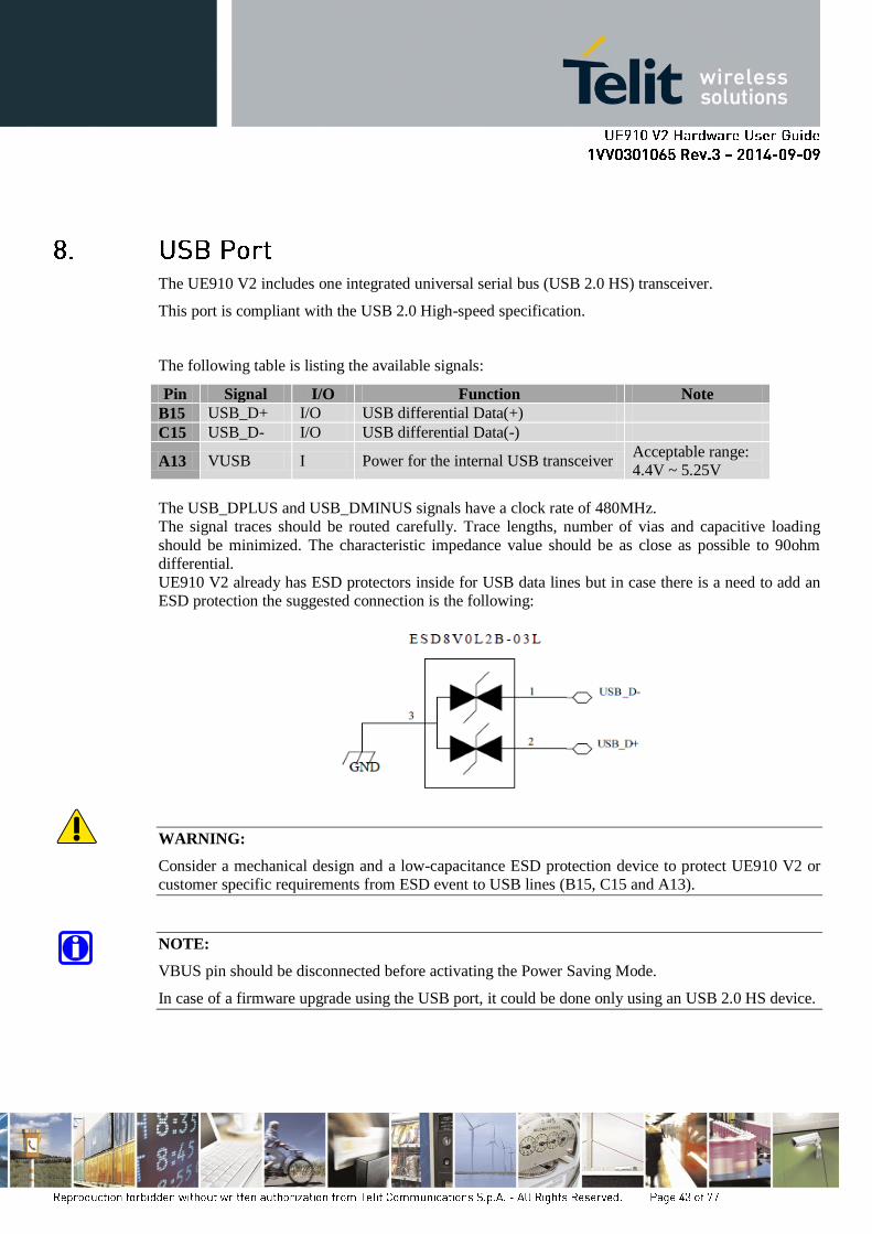
UE910 V2 already has ESD protectors inside for USB data lines but in case there is a need to add an
ESD protection the suggested connection is the following:
WARNING:
Consider a mechanical design and a low-capacitance ESD protection device to protect UE910 V2 or
customer specific requirements from ESD event to USB lines (B15, C15 and A13).
NOTE:
VBUS pin should be disconnected before activating the Power Saving Mode.
In case of a firmware upgrade using the USB port, it could be done only using an USB 2.0 HS device.
The UE910 V2 module is provided with by 1 Asynchronous serial port.
Modem Serial Port 1
Several configurations can be designed for the serial port on the OEM hardware, but the most
common are:
RS232 PC comport
Microcontroller [email protected](Universal Asynchronous Receiver Transmit)
Microcontroller UART@5V or other voltages different from 1.8V
Depending on the type of serial port on the OEM hardware, a level translator circuit may be needed to
make the system work.
On the UE910 V2 the ports are CMOS 1.8V.
The electrical characteristics of the serial port are explained in the following tables:
Absolute Maximum Ratings -Not Functional
Parameter Min Max
Input level on any digital pin(CMOS 1.8) with respect
to ground -0.3V +2.3V
Operating Range - Interface levels (1.8V CMOS)
Parameter Min Max
Input high level 1.5V 2.1 V
Input low level 0V 0.35V
Output high level 1.35V 1.8V
Output low level 0V 0.45V
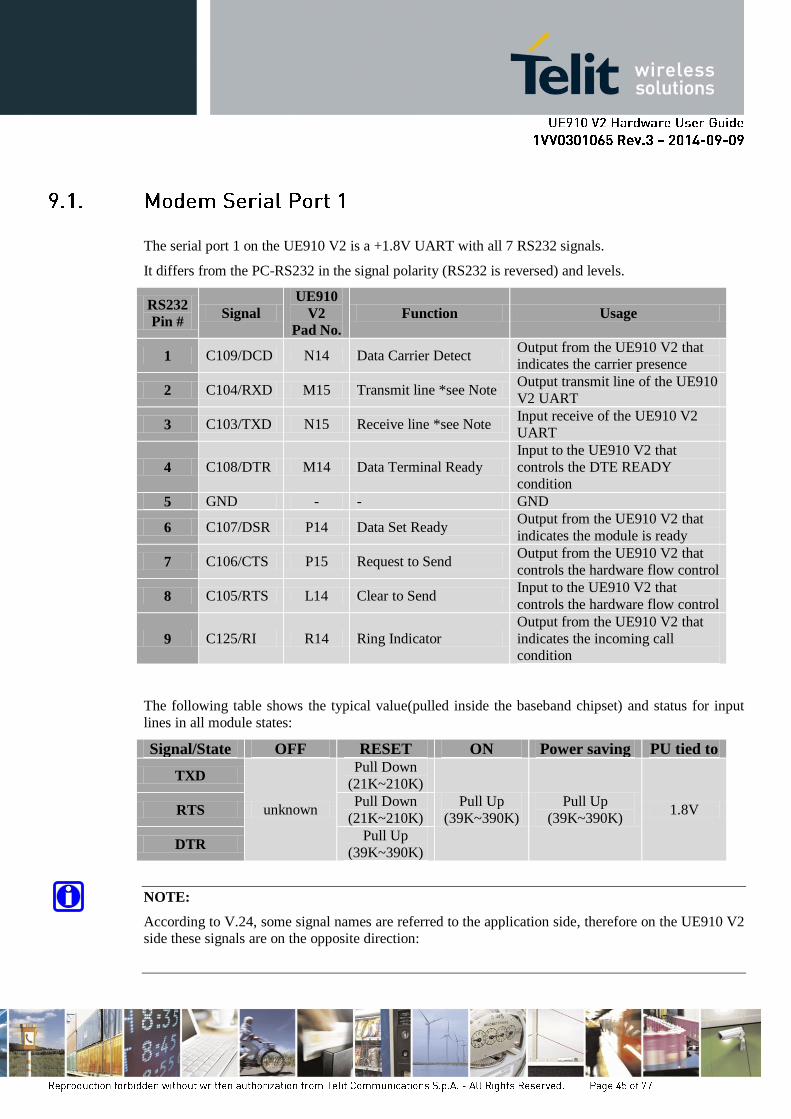
The serial port 1 on the UE910 V2 is a +1.8V UART with all 7 RS232 signals.
It differs from the PC-RS232 in the signal polarity (RS232 is reversed) and levels.
RS232
Pin # Signal
UE910
V2
Pad No.
Function Usage
1 C109/DCD N14 Data Carrier Detect Output from the UE910 V2 that
indicates the carrier presence
2 C104/RXD M15 Transmit line *see Note Output transmit line of the UE910
V2 UART
3 C103/TXD N15 Receive line *see Note Input receive of the UE910 V2
UART
4 C108/DTR M14 Data Terminal Ready
Input to the UE910 V2 that
controls the DTE READY
condition
5 GND - - GND
6 C107/DSR P14 Data Set Ready Output from the UE910 V2 that
indicates the module is ready
7 C106/CTS P15 Request to Send Output from the UE910 V2 that
controls the hardware flow control
8 C105/RTS L14 Clear to Send Input to the UE910 V2 that
controls the hardware flow control
9 C125/RI R14 Ring Indicator
Output from the UE910 V2 that
indicates the incoming call
condition
The following table shows the typical value(pulled inside the baseband chipset) and status for input
lines in all module states:
Signal/State OFF RESET ON Power saving PU tied to
TXD
unknown
Pull Down
(21K~210K)
Pull Up
(39K~390K)
Pull Up
(39K~390K) 1.8V RTS
Pull Down
(21K~210K)
DTR Pull Up
(39K~390K)
NOTE:
According to V.24, some signal names are referred to the application side, therefore on the UE910 V2
side these signals are on the opposite direction:
TXD on the application side will be connected to the receive line (here named C103/TXD)
RXD in the application side will be connected to the transmit line (here named C104/RXD)
NOTE:
For a minimum implementation, only the TXD and RXD lines must be connected, the other lines can
be left open provided a software flow control is implemented.
NOTE:
In order to avoid a back powering effect it is recommended to avoid having any HIGH logic level
signal applied to the digital pins of the UE910 V2 when the module is powered off or during an
ON/OFF transition.
NOTE:
High-speed UART supports up to 4Mbps. Please refer to the AT command User Guide in detail.
WARNING:
Consider a mechanical design and a low-capacitance ESD protection device to protect UE910 V2 or
customer specific requirements from ESD event to UART port (M15, N15, P15 and L14).
The secondary serial port on the UE910 V2 is not supported.
PAD Signal I/O Function Type
D15 Reserved - Reserved
E15 Reserved - Reserved
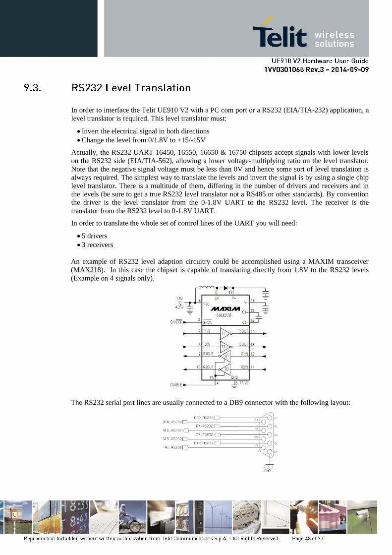
In order to interface the Telit UE910 V2 with a PC com port or a RS232 (EIA/TIA-232) application, a
level translator is required. This level translator must:
Invert the electrical signal in both directions
Change the level from 0/1.8V to +15/-15V
Actually, the RS232 UART 16450, 16550, 16650 & 16750 chipsets accept signals with lower levels
on the RS232 side (EIA/TIA-562), allowing a lower voltage-multiplying ratio on the level translator.
Note that the negative signal voltage must be less than 0V and hence some sort of level translation is
always required. The simplest way to translate the levels and invert the signal is by using a single chip
level translator. There is a multitude of them, differing in the number of drivers and receivers and in
the levels (be sure to get a true RS232 level translator not a RS485 or other standards). By convention
the driver is the level translator from the 0-1.8V UART to the RS232 level. The receiver is the
translator from the RS232 level to 0-1.8V UART.
In order to translate the whole set of control lines of the UART you will need:
5 drivers
3 receivers
An example of RS232 level adaption circuitry could be accomplished using a MAXIM transceiver
(MAX218). In this case the chipset is capable of translating directly from 1.8V to the RS232 levels
(Example on 4 signals only).
The RS232 serial port lines are usually connected to a DB9 connector with the following layout:
The UE910 V2 provides an analog audio interface and digital audio interface.
The UE910 V2 provides an analog audio interface; one differential input for audio to be
transmitted(Uplink) and a balanced output for audio to be received(Downlink).
The bias for the microphone has to be as clean as possible; the first connection (single ended) is
preferable since the Vmic noise and ground noise are fed into the input as common mode and then
rejected. This sounds strange; usually the connection to use in order to reject the common mode is the
balanced one. In this situation we have to recall that the microphone is a sound to current transducer,
so the resistor is the current to tension transducer, so finally the resistor feeds the input in balanced
way even if the configuration, from a microphone point of view, seems to be un-balanced.
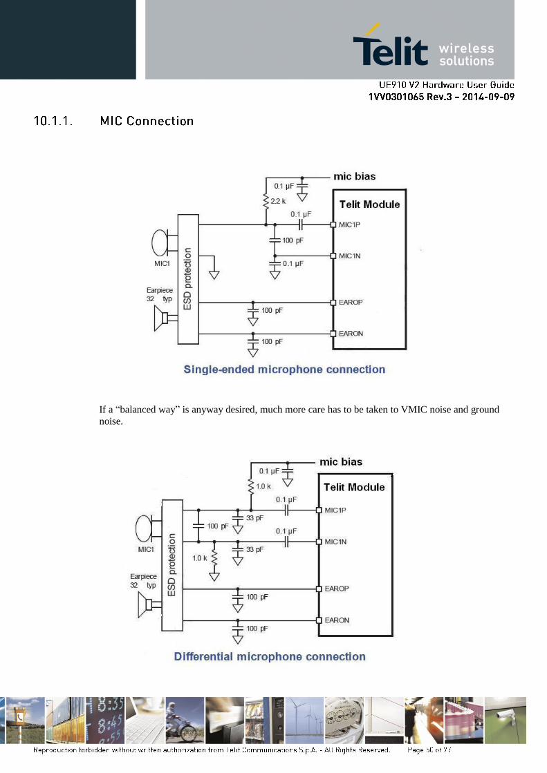
If a “balanced way” is anyway desired, much more care has to be taken to VMIC noise and ground
noise.
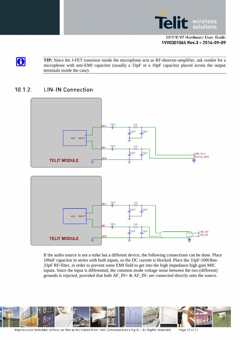
TIP: Since the J-FET transistor inside the microphone acts as RF-detector-amplifier, ask vendor for a
microphone with anti-EMI capacitor (usually a 33pF or a 10pF capacitor placed across the output
terminals inside the case).
If the audio source is not a mike but a different device, the following connections can be done. Place
100nF capacitor in series with both inputs, so the DC current is blocked. Place the 33pF-100Ohm-
33pF RF-filter, in order to prevent some EMI field to get into the high impedance high gain MIC
inputs. Since the input is differential, the common mode voltage noise between the two (different)
grounds is rejected, provided that both AF_IN+ & AF_IN- are connected directly onto the source.
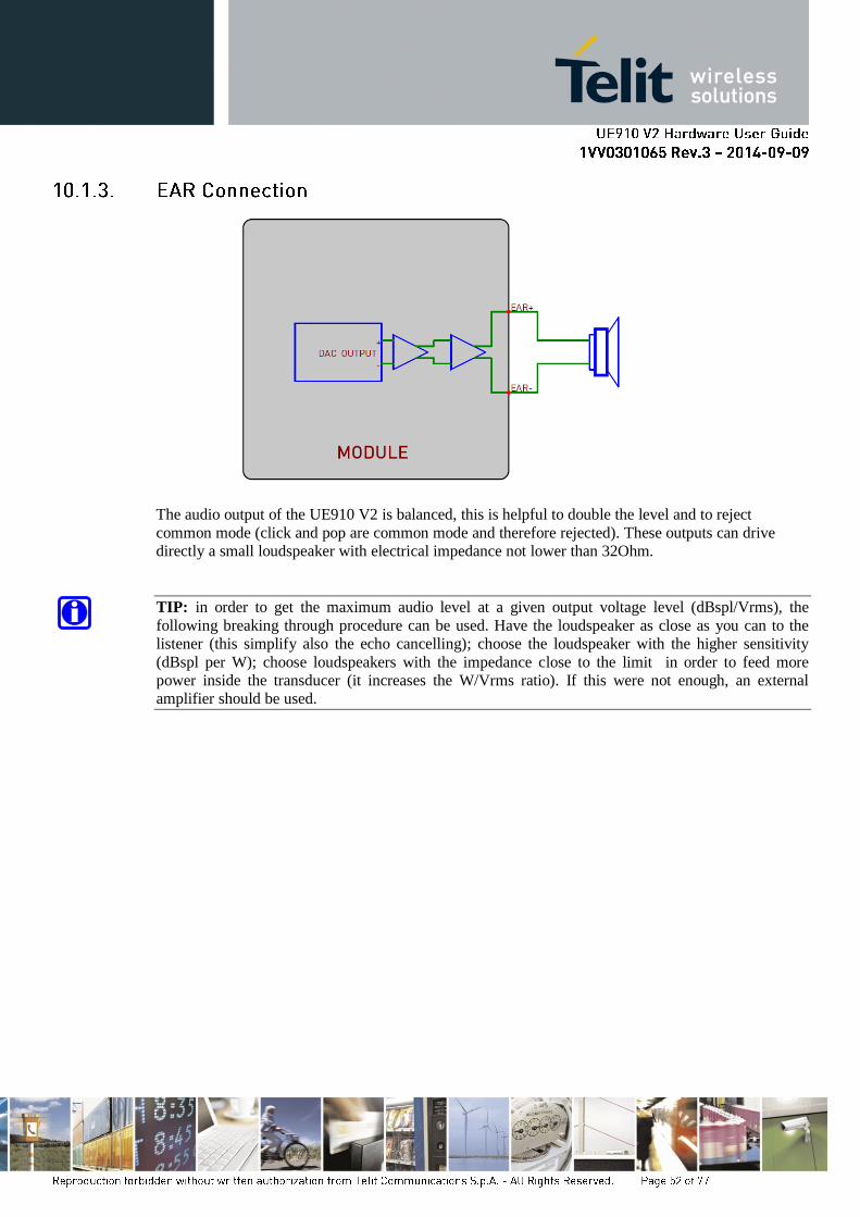
The audio output of the UE910 V2 is balanced, this is helpful to double the level and to reject
common mode (click and pop are common mode and therefore rejected). These outputs can drive
directly a small loudspeaker with electrical impedance not lower than 32Ohm.
TIP: in order to get the maximum audio level at a given output voltage level (dBspl/Vrms), the
following breaking through procedure can be used. Have the loudspeaker as close as you can to the
listener (this simplify also the echo cancelling); choose the loudspeaker with the higher sensitivity
(dBspl per W); choose loudspeakers with the impedance close to the limit in order to feed more
power inside the transducer (it increases the W/Vrms ratio). If this were not enough, an external
amplifier should be used.
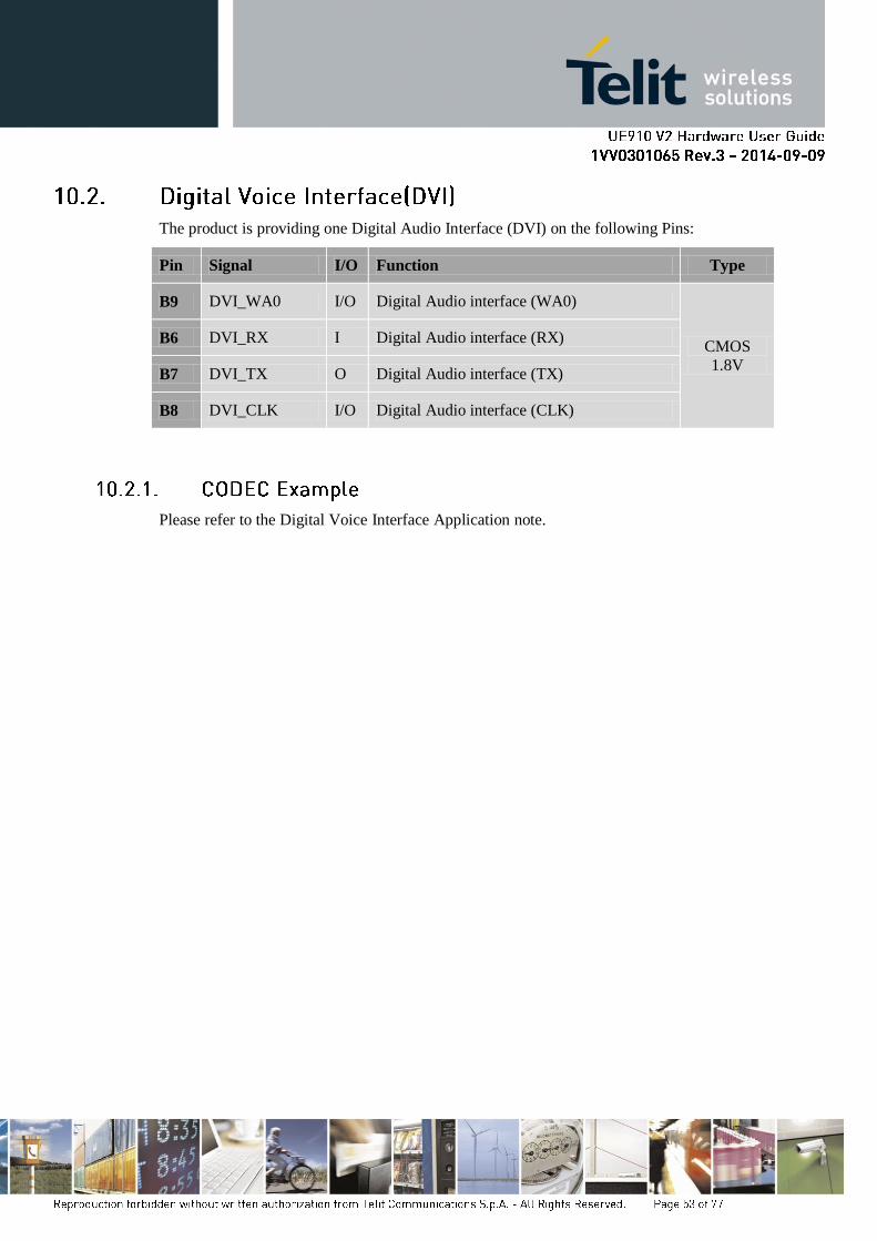
The product is providing one Digital Audio Interface (DVI) on the following Pins:
Pin Signal I/O Function Type
B9 DVI_WA0 I/O Digital Audio interface (WA0)
CMOS
1.8V
B6 DVI_RX I Digital Audio interface (RX)
B7 DVI_TX O Digital Audio interface (TX)
B8 DVI_CLK I/O Digital Audio interface (CLK)
Please refer to the Digital Voice Interface Application note.
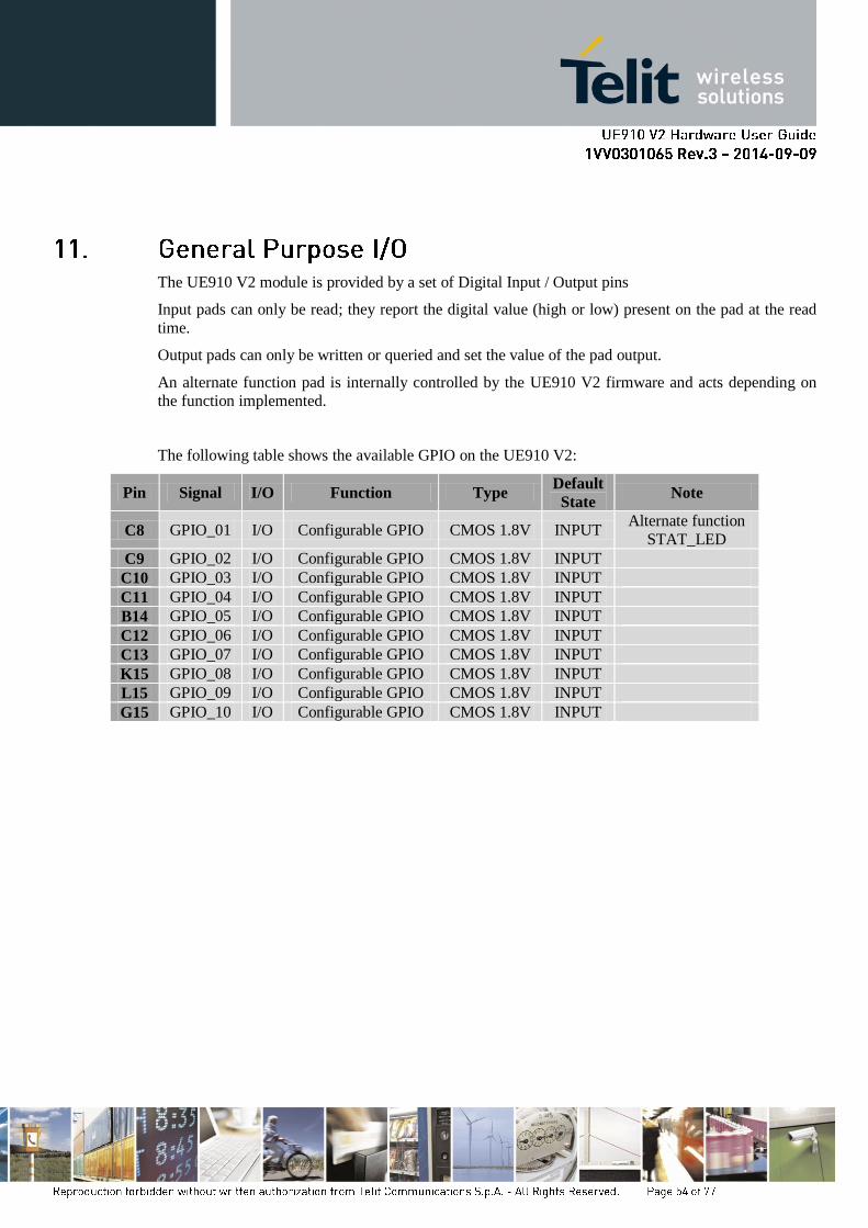
The UE910 V2 module is provided by a set of Digital Input / Output pins
Input pads can only be read; they report the digital value (high or low) present on the pad at the read
time.
Output pads can only be written or queried and set the value of the pad output.
An alternate function pad is internally controlled by the UE910 V2 firmware and acts depending on
the function implemented.
The following table shows the available GPIO on the UE910 V2:
Pin Signal I/O Function Type Default
State Note
C8 GPIO_01 I/O Configurable GPIO CMOS 1.8V INPUT Alternate function
STAT_LED
C9 GPIO_02 I/O Configurable GPIO CMOS 1.8V INPUT
C10 GPIO_03 I/O Configurable GPIO CMOS 1.8V INPUT
C11 GPIO_04 I/O Configurable GPIO CMOS 1.8V INPUT
B14 GPIO_05 I/O Configurable GPIO CMOS 1.8V INPUT
C12 GPIO_06 I/O Configurable GPIO CMOS 1.8V INPUT
C13 GPIO_07 I/O Configurable GPIO CMOS 1.8V INPUT
K15 GPIO_08 I/O Configurable GPIO CMOS 1.8V INPUT
L15 GPIO_09 I/O Configurable GPIO CMOS 1.8V INPUT
G15 GPIO_10 I/O Configurable GPIO CMOS 1.8V INPUT
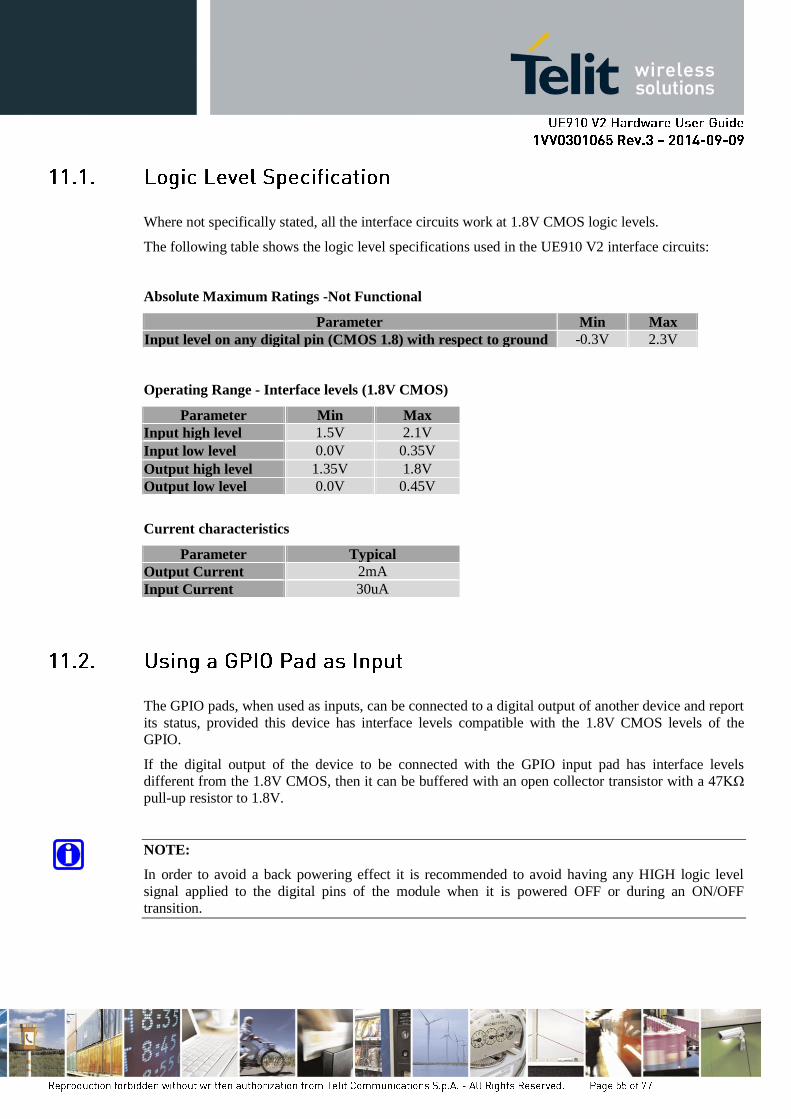
Where not specifically stated, all the interface circuits work at 1.8V CMOS logic levels.
The following table shows the logic level specifications used in the UE910 V2 interface circuits:
Absolute Maximum Ratings -Not Functional
Parameter Min Max
Input level on any digital pin (CMOS 1.8) with respect to ground -0.3V 2.3V
Operating Range - Interface levels (1.8V CMOS)
Parameter Min Max
Input high level 1.5V 2.1V
Input low level 0.0V 0.35V
Output high level 1.35V 1.8V
Output low level 0.0V 0.45V
Current characteristics
Parameter Typical
Output Current 2mA
Input Current 30uA
The GPIO pads, when used as inputs, can be connected to a digital output of another device and report
its status, provided this device has interface levels compatible with the 1.8V CMOS levels of the
GPIO.
If the digital output of the device to be connected with the GPIO input pad has interface levels
different from the 1.8V CMOS, then it can be buffered with an open collector transistor with a 47KΩ
pull-up resistor to 1.8V.
NOTE:
In order to avoid a back powering effect it is recommended to avoid having any HIGH logic level
signal applied to the digital pins of the module when it is powered OFF or during an ON/OFF
transition.
The GPIO pads, when used as outputs, can drive 1.8V CMOS digital devices or compatible hardware.
When set as outputs, the pads have a push-pull output and therefore the pull-up resistor may be
omitted.
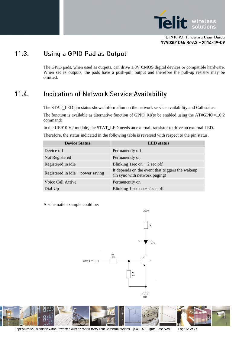
The STAT_LED pin status shows information on the network service availability and Call status.
The function is available as alternative function of GPIO_01(to be enabled using the AT#GPIO=1,0,2
command)
In the UE910 V2 module, the STAT_LED needs an external transistor to drive an external LED.
Therefore, the status indicated in the following table is reversed with respect to the pin status.
Device Status LED status
Device off Permanently off
Not Registered Permanently on
Registered in idle Blinking 1sec on + 2 sec off
Registered in idle + power saving It depends on the event that triggers the wakeup
(In sync with network paging)
Voice Call Active Permanently on
Dial-Up Blinking 1 sec on + 2 sec off
A schematic example could be:
The VRTC pin brings out the Real Time Clock supply, which is separate from the rest of the digital
part, allowing having only RTC going on when all the other parts of the device are off.
To this power output a backup capacitor can be added in order to increase the RTC autonomy during
power off of the battery. NO Devices must be powered from this pin.
In order to keep the RTC active when VBATT is not supplied it is possible to back up the RTC
section connecting a backup circuit to the related VRTC signal (pad C14 on module’s Pinout).
For additional details on the Backup solutions please refer to the related application note (xE910
RTC Backup Application Note)
For additional details on the Backup solutions please refer to the related application note (xE910
RTC Backup Application Note)
Bypass capacitor Min Typical Max
Pad no. C14 : VRTC 2.2uF - -
A regulated power supply output is provided in order to supply small devices from the module. This
output is active when the module is ON and goes OFF when the module is shut down. The operating
range characteristics of the supply are:
Operating Range – VAUX/PWRMON power supply
Parameter Min Typical Max
Output voltage 1.77V 1.8V 1.83V
Output current 200mA
Output bypass capacitor
(Inside the module) 2.2μF
The on board ADC is 10-bit converter. It is able to read a voltage level in the range of 0 ~ 1.2 volts
applied on the ADC pin input and store and convert it into 10 bit word.
Parameter Min Max Units
Input Voltage range 0 1.2 Volt
AD conversion - 10 bits
Resolution - 2 mV
Input Resistance 1 Mohm
The UE910 V2 provides one Analog to Digital Converter.
The input line is named as ADC_IN1 and it is available on pad B1.
An AT command is available to use the ADC function.
The command is AT#ADC=1,2. The read value is expressed in mV
Refer to SW User Guide or AT Commands Reference Guide for the full description of this function.
The UE910 V2 has been designed in order to be compliant with a standard lead-free SMT process.
The UE910 V2 overall dimensions are:
Length : 28.2 mm
Width : 28.2 mm
Thickness : 2.2 mm
Weight : 4.1 g
In order to easily rework the UE910 V2 it is suggested to consider having a 1.5 mm placement inhibit
area around the module on the application.
It is also suggested, as a common rule for an SMT component, to avoid having a mechanical part of
the application in direct contact with the module.
NOTE:
In the customer application, the region under WIRING INHIBIT (see figure) must be clear from
signal or ground paths.
Stencil’s apertures layout can be the same of the recommended footprint (1:1). We suggest a thickness
of stencil foil ≥ 120 µm.
Non solder mask defined (NSMD) type is recommended for the solder pads on the PCB.
The recommendation for the PCB pads dimensions are described in the following image(dimensions
in mm)
It is not recommended to place via or micro-via not covered by solder resist in an area of 0.3 mm
around the pads unless it carries the same signal as the pad itself (see following figure).
Holes in pad are allowed only for blind holes and not for through holes.
Recommendations for PCB Pad Surfaces:
Finish Layer thickness (um) Properties
Electro-less Ni / Immersion Au 3 ~ 7 / 0.05 ~ 0.15 good solder ability protection,
high shear force values
The PCB must be able to resist the higher temperatures which are occurring at the lead-free process.
This issue should be discussed with the PCB-supplier. Generally, the wettability of tin-lead solder
paste on the described surface plating is better compared to lead-free solder paste.
It is not necessary to panel the application’s PCB, however in that case it is suggested to use milled
contours and predrilled board breakouts; scoring or v-cut solutions are not recommended.
Lead free
Solder Paste Sn/Ag/Cu
We recommend using only “no clean” solder paste in order to avoid the cleaning of the modules after
assembly.
The following is the recommended solder reflow profile:
Profile Feature Pb-Free Assembly
Average ramp-up rate (TL to TP) 3℃/second max
Preheat
- Temperature Min (Tsmin)
- Temperature Max (Tsmax)
- Time (min to max) (ts)
150℃
200℃
60 ~ 180 seconds
Tsmax to TL
- Ramp-up Rate
3℃/second max
Time maintained above:
- Temperature (TL)
- Time (tL)
217℃
60 ~150 seconds
Peak Temperature (TP) 245 +0/-5℃
Time within 5℃ of actual Peak Temperature (tP) 10 ~30 seconds
Ramp-down Rate 6 ℃/sec max
Time 25℃ to Peak Temperature 8 minutes max
NOTE:
All temperatures refer to topside of the package, measured on the package body surface.
WARNING:
The UE910 V2 module withstands one reflow process only.

The UE910 V2 modules are packaged on trays of 20 pieces each. These trays can be used in SMT
processes for pick & place handling.


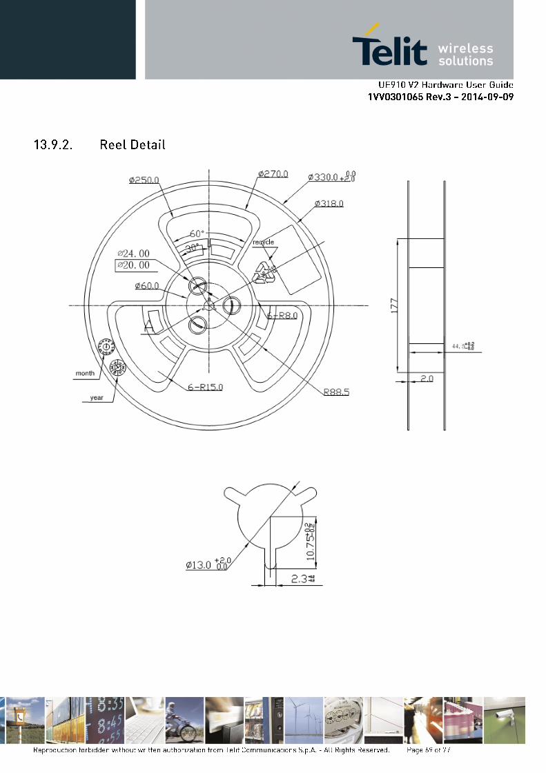
The UE910 V2 can be packaged on reel of 200 pieces each.
See figure for module positioning into the carrier.
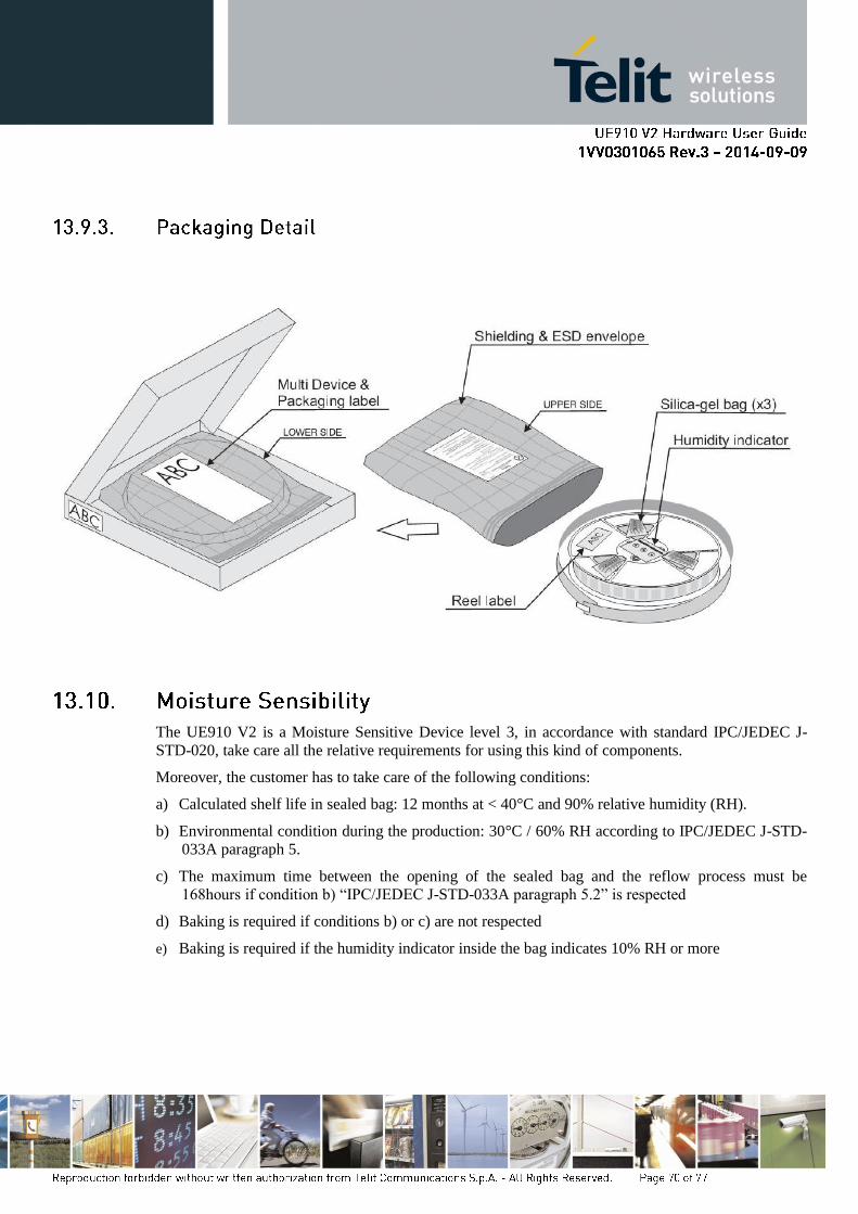
The UE910 V2 is a Moisture Sensitive Device level 3, in accordance with standard IPC/JEDEC J-
STD-020, take care all the relative requirements for using this kind of components.
Moreover, the customer has to take care of the following conditions:
a) Calculated shelf life in sealed bag: 12 months at < 40°C and 90% relative humidity (RH).
b) Environmental condition during the production: 30°C / 60% RH according to IPC/JEDEC J-STD-
033A paragraph 5.
c) The maximum time between the opening of the sealed bag and the reflow process must be
168hours if condition b) “IPC/JEDEC J-STD-033A paragraph 5.2” is respected
d) Baking is required if conditions b) or c) are not respected
e) Baking is required if the humidity indicator inside the bag indicates 10% RH or more

One of the following options should be chosen in the design of host system in order to download or
upgrade the Telit’s software and debug UE910 V2 when UE910 V2 is already mounted on a host
system.
CASE I:
Users who use both of UART and USB interfaces to communicate with UE910 V2 - Must implement a download method in a host system for upgrading UE910 V2 when it’s mounted.
CASE II:
Users who use USB interface only to communicate with UE910 V2 - Must arrange UART port in a host system for debugging or upgrading UE910 V2 when it’s mounted.
CASE III:
Users who use UART interface only to communicate with UE910 V2
- Must arrange USB port in a host system for debugging or upgrading UE910 V2 when it’s mounted.

READ CAREFULLY
Be sure the use of this product is allowed in the country and in the environment required. The use of
this product may be dangerous and has to be avoided in the following areas:
Where it can interfere with other electronic devices in environments such as hospitals, airports,
aircrafts, etc.
Where there is risk of explosion such as gasoline stations, oil refineries, etc.
It is the responsibility of the user to enforce the country’s regulations and the specific environmental
regulation.
Do not disassemble the product; any mark of tampering will compromise the warranty validity.
We recommend following the instructions of the hardware user guides for a correct wiring of the
product. The product has to be supplied with a stabilized voltage source and the wiring has to be
conforming to the security and fire prevention regulations.
The product has to be handled with care, avoiding any contact with the pads because electrostatic
discharges may damage the product itself. Same cautions have to be taken for the SIM, checking
carefully the instruction for its use. Do not insert or remove the SIM when the product is in power
saving mode.
The system integrator is responsible for the functioning of the final product; therefore, care has to be
taken to the external components of the module, as well as of any project or installation issue, because
of the risk of disturbing the GSM/WCDMA network or external devices or having impact on the
security. Should there be any doubt, please refer to the technical documentation and the regulations in
force.
Every module has to be equipped with a proper antenna with specific characteristics. The antenna has
to be installed with care in order to avoid any interference with other electronic devices and has to
guarantee a minimum distance from the body (20 cm). In case this requirement cannot be satisfied,
the system integrator has to assess the final product against SAR regulations.
The Telit UE910-EU V2 module has been evaluated against the essential requirements of the
1999/5/EC Directive.
The conformity assessment procedure referred to in Article 10 and detailed in Annex IV of Directive
1999/5/EC has been followed with the involvement of the following Notified Body:
AT4 wireless S.A.
Parque Technologico de Andalucia
C/ Severo Ochoa 2
29590 Campanillas – Malaga
SPAIN
Notified Body No: 1909
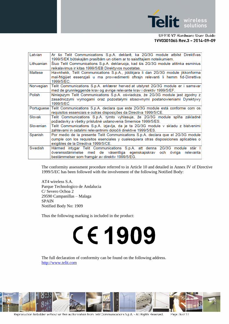
Thus the following marking is included in the product:
The full declaration of conformity can be found on the following address.
http://www.telit.com

There is no restriction for the commercialization of the UE910-EU V2 module in all the countries of
the European Union.
Final product integrating this module must be assessed gainst essential requirements of the
1999/5/EC(R&TTE) Directive. It should be noticed that assessment does not necessarily lead to
testing. Telit Communications S.p.A recommends carrying out the following assessments:
Alternately, assessment of the final product against EMC(Art. 3.1b) and Electrical safety(Art. 3.1a)
Essential requirements can be done against the essential requirements of the EMC and the LVD
Directives:
Low Voltage Directive 2006/95/EC and product safety
Directive EMC 2004/108/EC for conformity for EMC

Modification statement
Telit has not approved any changes or modifications to this device by the user. Any changes or
modifications could void the user’s authority to operate the equipment.
Telit n’approuve aucune modification apportée à l’appareil par l’utilisateur, quelle qu’en soit la
nature. Tout changement ou modification peuvent annuler le droit d’utilisation de l’appareil par
l’utilisateur.
Interference statement
This device complies with Part 15 of the FCC Rules and Industry Canada licence-exempt RSS
standard(s). Operation is subject to the following two conditions: (1) this device may not cause
interference, and (2) this device must accept any interference, including interference that may cause
undesired operation of the device.
Le présent appareil est conforme aux CNR d'Industrie Canada applicables aux appareils radio
exempts de licence. L'exploitation est autorisée aux deux conditions suivantes : (1) l'appareil ne doit
pas produire de brouillage, et (2) l'utilisateur de l'appareil doit accepter tout brouillage
radioélectrique subi, même si le brouillage est susceptible d'en compromettre le fonctionnement.
Wireless notice
This equipment complies with FCC and IC radiation exposure limits set forth for an uncontrolled
environment. The antenna should be installed and operated with minimum distance of 20 cm between
the radiator and your body. Antenna gain must be below:
Frequency band UE910-NA V2
GSM850 8.1 dBi
WCDMA FDD V 11.09 dBi
PCS1900 3.51 dBi
WCDMA FDD II 9.83 dBi
This transmitter must not be co-located or operating in conjunction with any other antenna or
transmitter.
Cet appareil est conforme aux limites d'exposition aux rayonnements de la IC pour un environnement
non contrôlé. L'antenne doit être installé de façon à garder une distance minimale de 20 centimètres
entre la source de rayonnements et votre corps. Gain de l'antenne doit être ci-dessous:
Frequency band UE910-NA V2
GSM850 8.1 dBi
WCDMA FDD V 11.09 dBi
PCS1900 3.51 dBi
WCDMA FDD II 9.83 dBi

L'émetteur ne doit pas être colocalisé ni fonctionner conjointement avec à autre antenne ou autre
émetteur.
FCC Class B digital device notice
This equipment has been tested and found to comply with the limits for a Class B digital device,
pursuant to part 15 of the FCC Rules. These limits are designed to provide reasonable protection
against harmful interference in a residential installation. This equipment generates, uses and can
radiate radio frequency energy and, if not installed and used in accordance with the instructions, may
cause harmful interference to radio communications. However, there is no guarantee that interference
will not occur in a particular installation. If this equipment does cause harmful interference to radio or
television reception, which can be determined by turning the equipment off and on, the user is
encouraged to try to correct the interference by one or more of the following measures:
- Reorient or relocate the receiving antenna.
- Increase the separation between the equipment and receiver.
- Connect the equipment into an outlet on a circuit different from that to which the receiver is
connected.
- Consult the dealer or an experienced radio/TV technician for help.
Labeling on Host product statements
Host system including UE910-NA V2 must be labeled with
“Contains FCC ID:RI7UE910NAV2 and IC ID:5131A-UE910NAV2”.