sonochemical approach for rapid growth of zinc...
TRANSCRIPT

Sonochemical Approach for Rapid Growth of Zinc Oxide Nanowalls
Avinash P. Nayak1,*
, Aaron M. Katzenmeyer2,†, Yasuhiro Gosho
3,¥, M. Saif Islam2, ‡.
*[email protected], †[email protected], ¥[email protected], ‡[email protected].
Department of Electrical Engineering, University of California - Davis, Davis, 95616, USA
Abstract:
In this report, we propose a new approach to synthesize ZnO (zinc oxide) nanowalls (NWall)on
aluminum and alumina coated substrates at room ambient conditions. The synthesized ZnO
NWalls are uniform and highly dense in areas where Al or Al2O3 (Alumina) is present. The
height and thickness of these ZnO NWalls average at 0.8µm-1.5µm to 20nm respectively.
Photoluminescence (PL) measurements, transmission electron microscopy (TEM) images, UV
Vis spectroscopy, SEM-EDS results indicate NWalls composed of ZnO. The sonochemical
synthesis was tried on Si, SiO2, Cr, and Ag but did not result in NWalls. We find that the growth
of ZnO NWalls only form on Al or alumina. We attribute the formation of Al assisted ZnO
nanowall growth to the phase transformations that occur under high-pressure, high-temperature,
and chemical growth kinetics. The deposition method reported is applicable to Al coated non-
metallic surfaces such as glass and we show the as-formed NWalls function as UV
photoconductors.
Keywords: Zinc Oxide, Nanowalls, Sonochemistry, Solution Growth, Ultrasound, Self-
Organization, Selective Deposition.
Introduction:
Zinc oxide (ZnO) has a relatively large bandgap (3.37eV) in comparison to traditional
semiconductors such as silicon (1.12eV), germanium (0.66eV), indium phosphide (1.27eV) and
galium phoshide (2.25eV). This large bandgap is of great interest for photonic applications[1]
,
solar cells[2]
, and gas sensors[3]
. The physical characeteristics of ZnO material have also been
widley explored. Quantum dots[4]
, nanobelts[5]
, nanotubes[6]
, and nanowires[7]
are just a few of
the structures that have been synthesised. Using a metal catalyst, high temperature and vapor-
liquid-process (VLS) process ZnO nanowalls were synthesied[8]
. Using such a process however,
requires extensive time for growth. ZnO nanowalls grown by metalorganic chemical vapor
depositon (MOCVD) has also been reported. This requires an ellaborate setup enclosed in a
pressurized chamber to grow NWalls at relatively low tempereature (~500oC).
[9] This
temperature is too high for many possible device applications. Here we report on a simple
sonochemical method of growth that does not require external input of high temperature or
pressure.
For fast process, high density, uniform growth of ZnO nanowalls, we use a simple and
inexpensive method for growing ZnO nanowalls in ten minutes. Herein, we report on a new
sonochemical deposition technique to selectively deposit ZnO nanowalls on Al or alumina
coated substrates. To our knowledge, no one has adopted this sonochemical method to synthesize
ZnO nanowalls. The room ambient process reported in this paper greatly reduces the time down
to ten minutes for the synthesis of ZnO nanowalls. Scanning electron microscopy (SEM),
absorbtion spectroscopy (UV-Vis), photomuminascence (PL), field emission energy dispersive
spectroscopy (EDS), transmission electron microscopy (TEM) have been used to investigate the
ZnO nanowall structure. The foramtion of these ZnO NWalls is mainly due to the phase
transfomrations that take place under high-pressure and high-temperature caused by the
cavitation bubbles.Growth kinetics of ZnO NWalls are explained by observing growth in three
minute intervals.

Experimental:
The growth of ZnO NWalls was performed using only one system (750W ultrasonic processor,
Sonics and Systems). A solution of 0.02M zinc nitrate hexahydrate (Zn (NO3)2.6H2O, 99.998%)
and 0.02M hexamethylenetetramine (HMT, (CH2) .6N4, 99
+ %) which was first stirred with a
magnetic stir bar at 350 r.p.m for 5 minutes to ensure a mixed solution was used as the only
solution for the growth of ZnO nanowalls. The Al coated substrate was immersed onto the
aqueous solution and sonicated at 50% of the maximum amplitude (21Wcm-2
) of the 20 kHz
ultrasonic probe for 10 minutes. The sample was then rinsed with DI water and dried with a N2
gun for characterization. FE-SEM was performed using a LEO 1550,Hitachi S-4500, or FEI
XL30-SFEG. UV-Vis used was performed using a Perkin Elmer Lambda 750 spectrometer. A
325 nm HeCd laser (Melles Griot) was used to collect the photoluminescence spectrum. All
chemical reagents used in this report were used without further purification.
To understand the growth kinetics, an Al coated Si substrate was immersed into a beaker
containing zinc nitrate hexahydrate and HMTA. The sample was incrementally extracted from
the beaker in three minute intervals.
Sunray 400 SM 100mW/cm2 UVA light (320–390nm) flood-lamp to test for photoconductivity.
Results and discussion:
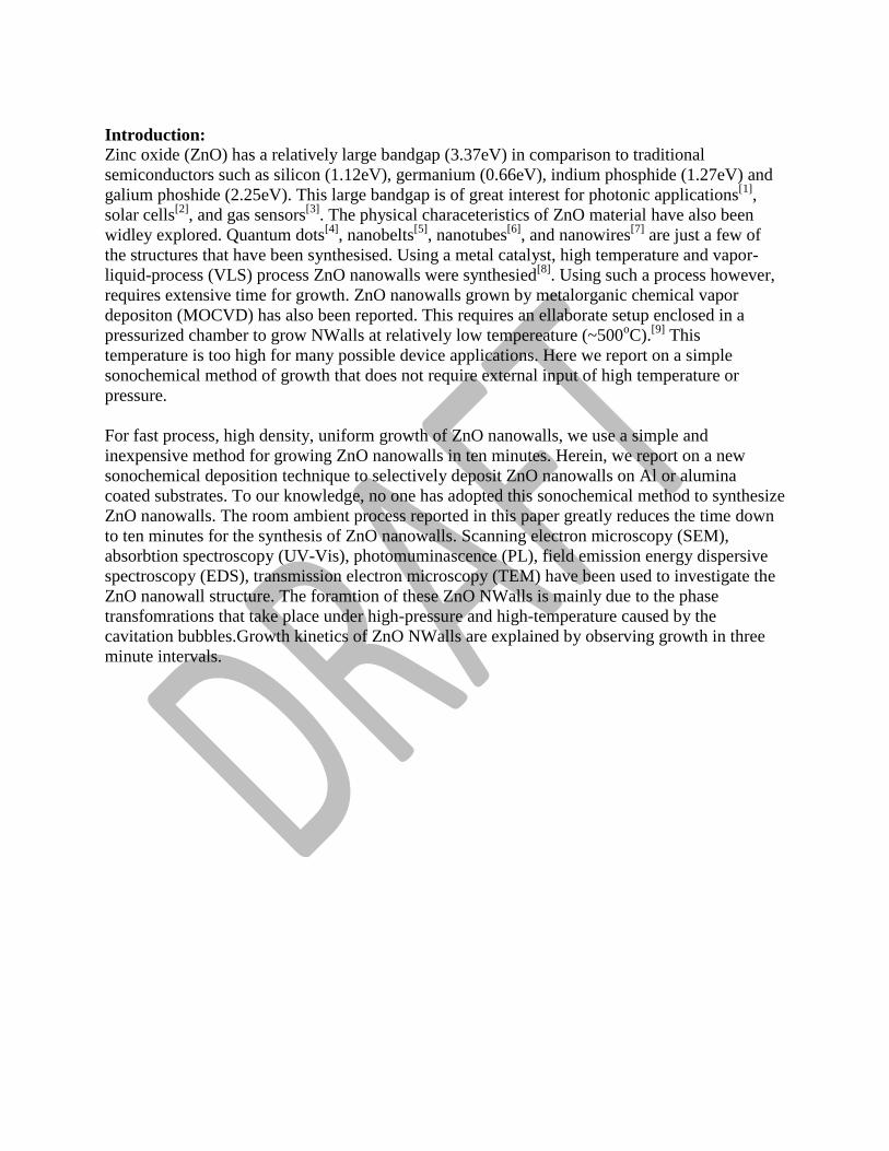
All zinc oxide nanowalls reported were synthesized using the same experimental parameters
stated in the experimental section except in some cases; a seed layer was first deposited. We find
however that this deposition however is not required for the formation of ZnO nanowalls. Figure
1a shows the ZnO NWalls grown from 6nm of an Al coated Si substrate. The thickness of each
wall is ~10-15nm. The average length of these nanowalls is 0.8µm-1.5µm as seen in the inset.
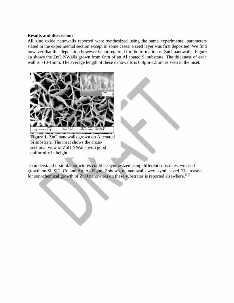
To understand if similar structures could be synthesized using different substrates, we tried
growth on Si, SiC, Cr, and Ag. As Figure 2 shows, no nanowalls were synthesized. The reason
for sonochemical growth of ZnO nanowires on these substrates is reported elsewhere.[10]
Figure 1. ZnO nanowalls grown on Al coated
Si substrate. The inset shows the cross-
sectional view of ZnO NWalls with good
uniformity in height.
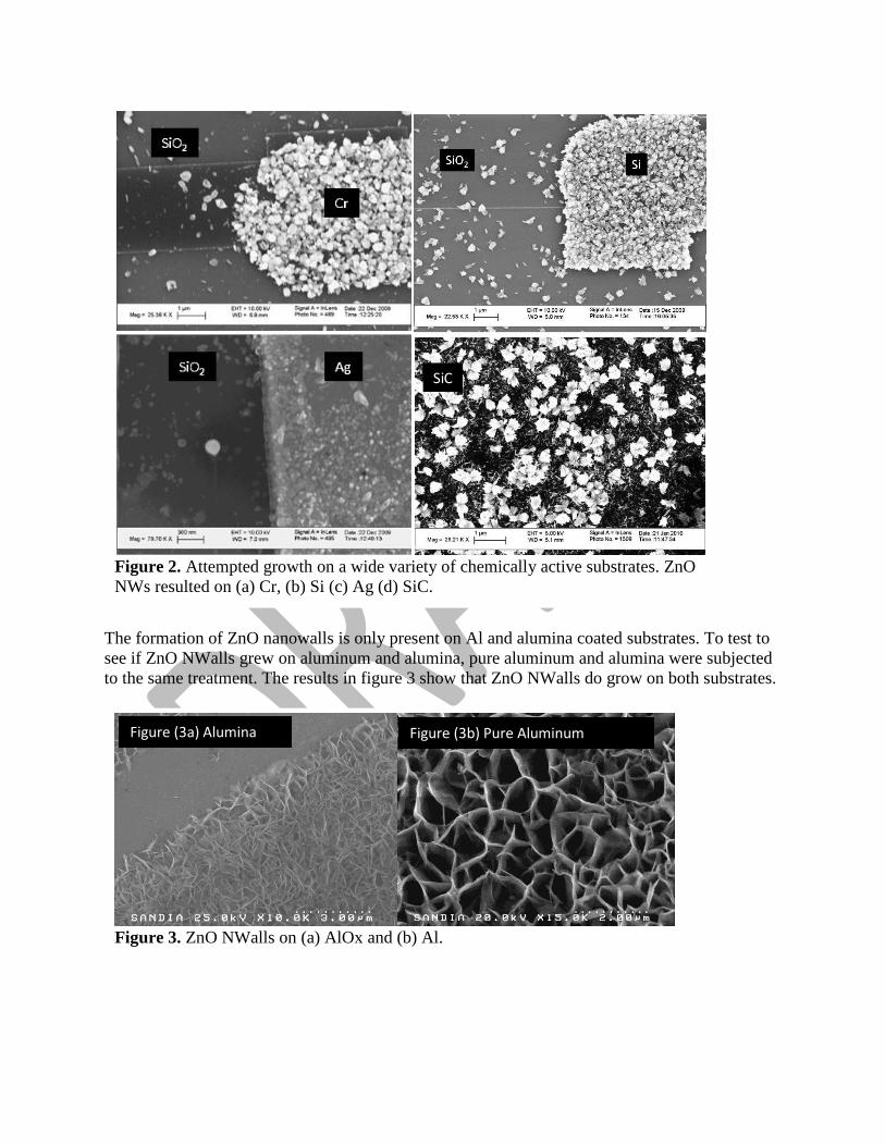
The formation of ZnO nanowalls is only present on Al and alumina coated substrates. To test to
see if ZnO NWalls grew on aluminum and alumina, pure aluminum and alumina were subjected
to the same treatment. The results in figure 3 show that ZnO NWalls do grow on both substrates.
Figure 3. ZnO NWalls on (a) AlOx and (b) Al.
Figure (3a) Alumina Figure (3b) Pure Aluminum
SiC
Figure 2. Attempted growth on a wide variety of chemically active substrates. ZnO
NWs resulted on (a) Cr, (b) Si (c) Ag (d) SiC.
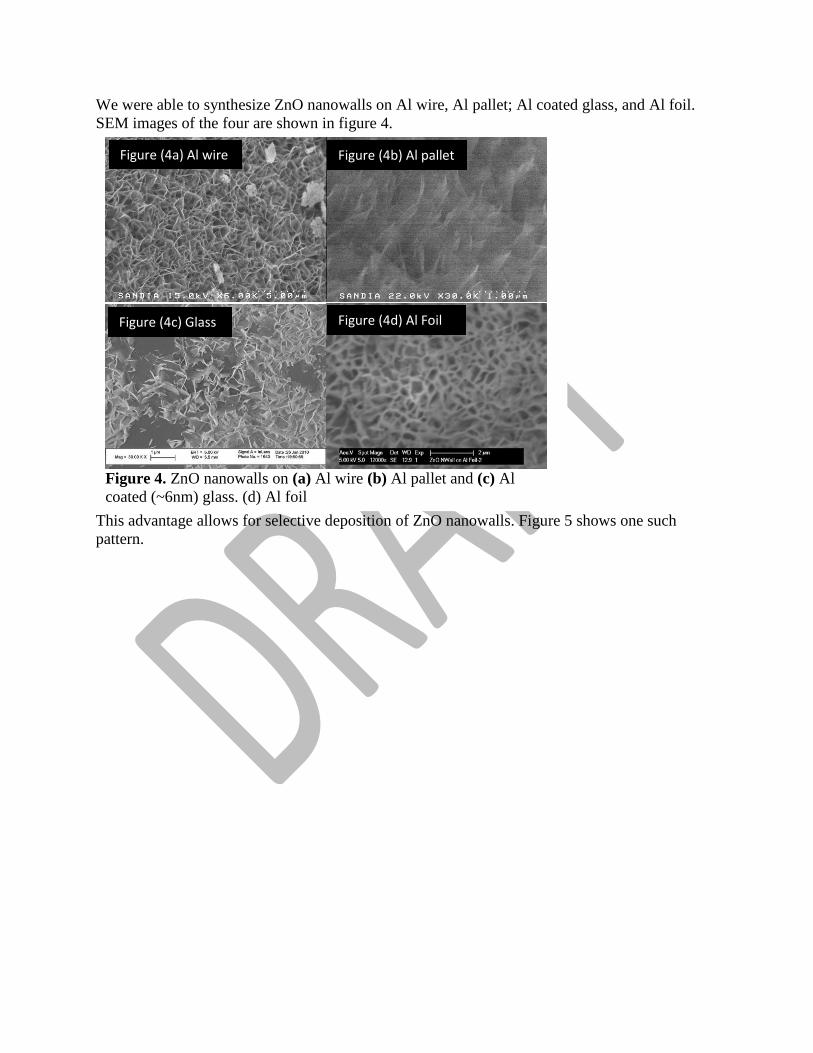
We were able to synthesize ZnO nanowalls on Al wire, Al pallet; Al coated glass, and Al foil.
SEM images of the four are shown in figure 4.
This advantage allows for selective deposition of ZnO nanowalls. Figure 5 shows one such
pattern.
Figure 4. ZnO nanowalls on (a) Al wire (b) Al pallet and (c) Al
coated (~6nm) glass. (d) Al foil
Figure (4a) Al wire Figure (4b) Al pallet
Figure (4c) Glass Figure (4d) Al Foil

In the growth process, elemental Al is consumed as is evident from transmission experiments.
The spectroscopy results showing the transparency of ZnO nanowall electrodes is shown in
figure 6. The transparency increases by ~10% after growth.
AlPtSi02
Al
Al
Al
Si02
Si02
Pt
Al
Si02
Figure 5. Selective deposition of ZnO nanowalls on Al electrodes.
Al
Al Al
SiO2

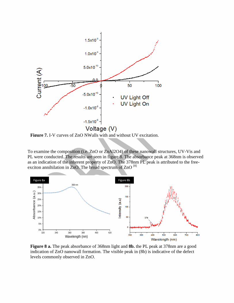
Dark and UV photocurrents of a NWall film are plotted in figure 7. The measurements were
done on a processed sample of 6nm Al on glass with separation distance between the two
tungsten probe tips was ~10µm. The reason for low conductivity even in the presence of
ultraviolet (UV) light is attributed to the formation of ZnAl2O4 during the growth of these
nanowalls. The chemical growth kinetics for the formation of these ZnO NWalls is explained in
the succeeding section. It has been reported that ZnAl2O4 is lower in electrical conductivity than
ZnO and other oxide mixtures.[11]
Figure 6. Transparency results before and after ZnO NWall growth for different thickness’
of Al. The Al undergoes chemical modification or consumption as a result of the growth
process. The inset shows the optical images of the processed and unprocessed samples.
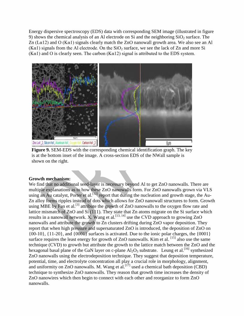
To examine the composition (i.e. ZnO or ZnAl2O4) of these nanowall structures, UV-Vis and
PL were conducted. The results are seen in figure 8. The absorbance peak at 368nm is observed
as an indication of the inherent property of ZnO. The 378nm PL peak is attributed to the free-
exciton annihilation in ZnO. The broad spectrum of ZnO [8]
368 nm
0%
5%
10%
15%
20%
25%
30%
35%
40%
320 340 360 380 400 420
Absorb
ance (
a.u
.)
Wavelength (nm)
Figure 8 a. The peak absorbance of 368nm light and 8b. the PL peak at 378nm are a good
indication of ZnO nanowall formation. The visible peak in (8b) is indicative of the defect
levels commonly observed in ZnO.
Figure 7. I-V curves of ZnO NWalls with and without UV excitation.
Figure 8a Figure 8b
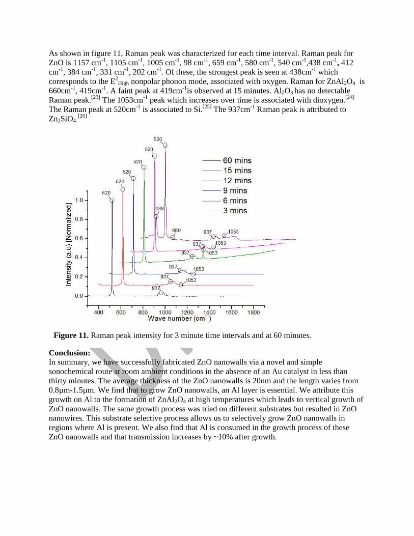
Energy dispersive spectroscopy (EDS) data with corresponding SEM image (illustrated in figure
9) shows the chemical analysis of an Al electrode on Si and the neighboring SiO2 surface. The
Zn (Lα12) and O (Kα1) signals clearly match the ZnO nanowall growth area. We also see an Al
(Kα1) signals from the Al electrode. On the SiO2 surface, we see the lack of Zn and more Si
(Kα1) and O is clearly seen. The carbon (Kα12) signal is attributed to the EDS system.
Growth mechanism:
We find that no additional seed-layer is necessary beyond Al to get ZnO nanowalls. There are
multiple explanations as to how these ZnO nanowalls form. For ZnO nanowalls grown via VLS
using an Au catalyst, Porter et al.[12]
report that during the nucleation and growth stage, the Au-
Zn alloy forms ripples instead of dots which allows for ZnO nanowall structures to form. Growth
using MBE by Fan et al.[3]
attribute the growth of ZnO nanowalls to the oxygen flow rate and
lattice mismatch of ZnO and Si (111). They state that Zn atoms migrate on the Si surface which
results in a nanowall network. X. Wang et al.[13, 14]
use the CVD approach to growing ZnO
nanowalls and attribute the growth to Zn clusters drifting during ZnO vapor deposition. They
report that when high pressure and supersaturated ZnO is introduced, the deposition of ZnO on
{00-10}, {11-20}, and {0001} surfaces is activated. Due to the ionic polar charges, the {0001}
surface requires the least energy for growth of ZnO nanowalls. Kim et al. [15]
also use the same
technique (CVD) to growth but attribute the growth to the lattice match between the ZnO and the
hexagonal basal plane of the GaN layer on c-plane Al2O3 substrate. Leung et al.[16]
synthesized
ZnO nanowalls using the electrodeposition technique. They suggest that deposition temperature,
potential, time, and electrolyte concentration all play a crucial role in morphology, alignment,
and uniformity on ZnO nanowalls. M. Wang et al.[17]
used a chemical bath deposition (CBD)
technique to synthesize ZnO nanowalls. They reason that growth time increases the density of
ZnO nanowires which then begin to connect with each other and reorganize to form ZnO
nanowalls.
Figure 9. SEM-EDS with the corresponding chemical identification graph. The key
is at the bottom inset of the image. A cross-section EDS of the NWall sample is
shown on the right.

The PL spectra for the ZnO nanowall sample (figure 8b) that we synthesized sonochemically,
indicate that the ZnO nanowall growth is mediated by the presence of aluminum oxide.
Aluminum oxide produced at low temperature shows two PL peaks between 400-500nm.[18]
The
induced high pressure and temperature from the cavitation bubble imploding produces AlOOH
during cavitation.. The zinc/aluminum interface allows for zinc aluminate (ZnAl2O4) or “spinel”
to form.[19]
The reaction between Zn(OH)2 and AlOOH allows for the formation of ZnAl2O4, this
zinc aluminate has been synthesized in a hydrothermal solution at high temperatures.[20]
HMTA
and ZnAl2O4 would then support the vertical growth {0001} of ZnO nanowalls. We find that the
ZnO nanowalls grow perpendicular to the alumina/spinel interface.
The chemical reaction that is undertaken is stated in [equations 1-7][10, 21, 22]
:
(CH2)6N4 + 6H2O 4NH3 + 6HCHO [1]
NH3 + H2O NH4+
+ OH-
[2]
Zn(NO3)6H2O Zn2+
+ 2NO3-
[3]
Zn2+
+ 2OH- Zn(OH)2 [4]
Zn(OH)2 ZnO + H2O [5]
Al + 2H2O 1.5H2 + (AlO)OH [6]
From [4] and [6]:
Zn(OH)2 + 2AlO(OH) ZnAl2O4 + 2H2O [7]
To find at what time the formation of ZnO nanowalls occur, we observe growth in three minute
intervals. The experimental procedure is presented in the experimental section. The results are
shown in figure 10. We see that within nine minutes, ZnO nanowalls have formed. Within six
minutes, spinel clusters form which suppliment the growth of ZnO in the vertical direction.
Figure 10. Growth kinetics for the formation of ZnO NWalls at (a) 3 minutes (b) 6 minutes
(c) 9 minutes (d) 12 minutes (e) 15 minutes and (f) 60 minutes.
a. 3 minutes b. 6 minutes
d. 12 minutes e. 15 minutes
c. 9 minutes
f. 60 minutes
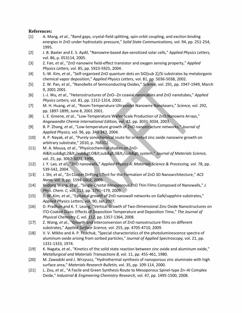
As shown in figure 11, Raman peak was characterized for each time interval. Raman peak for
ZnO is 1157 cm-1
, 1105 cm-1
, 1005 cm-1
, 98 cm-1
, 659 cm-1
, 580 cm-1
, 540 cm-1
,438 cm-1
, 412
cm-1
, 384 cm-1
, 331 cm-1
, 202 cm-1
. Of these, the strongest peak is seen at 438cm-1
which
corresponds to the E2
High nonpolar phonon mode, associated with oxygen. Raman for ZnAl2O4 is
660cm-1
, 419cm-1
. A faint peak at 419cm-1
is observed at 15 minutes. Al2O3 has no detectable
Raman peak.[23]
The 1053cm-1
peak which increases over time is associated with dioxygen.[24]
The Raman peak at 520cm-1
is associated to Si.[25]
The 937cm-1
Raman peak is attributed to
Zn2SiO4 [26]
Conclusion:
In summary, we have successfully fabricated ZnO nanowalls via a novel and simple
sonochemical route at room ambient conditions in the absence of an Au catalyst in less than
thirty minutes. The average thickness of the ZnO nanowalls is 20nm and the length varies from
0.8µm-1.5µm. We find that to grow ZnO nanowalls, an Al layer is essential. We attribute this
growth on Al to the formation of ZnAl2O4 at high temperatures which leads to vertical growth of
ZnO nanowalls. The same growth process was tried on different substrates but resulted in ZnO
nanowires. This substrate selective process allows us to selectively grow ZnO nanowalls in
regions where Al is present. We also find that Al is consumed in the growth process of these
ZnO nanowalls and that transmission increases by ~10% after growth.
Figure 11. Raman peak intensity for 3 minute time intervals and at 60 minutes.
References: [1] A. Mang, et al., "Band gaps, crystal-field splitting, spin-orbit coupling, and exciton binding
energies in ZnO under hydrostatic pressure," Solid State Communications, vol. 94, pp. 251-254, 1995.
[2] J. B. Baxter and E. S. Aydil, "Nanowire-based dye-sensitized solar cells," Applied Physics Letters, vol. 86, p. 053114, 2005.
[3] Z. Fan, et al., "ZnO nanowire field-effect transistor and oxygen sensing property," Applied Physics Letters, vol. 85, pp. 5923-5925, 2004.
[4] S.-W. Kim, et al., "Self-organized ZnO quantum dots on SiO[sub 2]/Si substrates by metalorganic chemical vapor deposition," Applied Physics Letters, vol. 81, pp. 5036-5038, 2002.
[5] Z. W. Pan, et al., "Nanobelts of Semiconducting Oxides," Science, vol. 291, pp. 1947-1949, March 9, 2001 2001.
[6] J.-J. Wu, et al., "Heterostructures of ZnO--Zn coaxial nanocables and ZnO nanotubes," Applied Physics Letters, vol. 81, pp. 1312-1314, 2002.
[7] M. H. Huang, et al., "Room-Temperature Ultraviolet Nanowire Nanolasers," Science, vol. 292, pp. 1897-1899, June 8, 2001 2001.
[8] L. E. Greene, et al., "Low-Temperature Wafer-Scale Production of ZnO Nanowire Arrays," Angewandte Chemie International Edition, vol. 42, pp. 3031-3034, 2003.
[9] B. P. Zhang, et al., "Low-temperature growth of ZnO nanostructure networks," Journal of Applied Physics, vol. 96, pp. 340-343, 2004.
[10] A. P. Nayak, et al., "Purely sonochemical route for oriented zinc oxide nanowire growth on arbitrary substrate," 2010, p. 768312.
[11] M. A. Mousa, et al., "Physicochemical studies on ZnO-Al<sub>2</sub>O<sub>3</sub> system," Journal of Materials Science, vol. 25, pp. 3067-3071, 1990.
[12] J. Y. Lao, et al., "ZnO nanowalls," Applied Physics A: Materials Science & Processing, vol. 78, pp. 539-542, 2004.
[13] J. Shi, et al., "Zn Cluster Drifting Effect for the Formation of ZnO 3D Nanoarchitecture," ACS Nano, vol. 3, pp. 1594-1602, 2009.
[14] Xudong Wang, et al., "Single-Crystal Mesoporous ZnO Thin Films Composed of Nanowalls," J. Phys. Chem. C, vol. 113, pp. 1791–179, 2009.
[15] S. W. Kim, et al., "Epitaxial growth of ZnO nanowall networks on GaN/sapphire substrates," Applied Physics Letters, vol. 90, Jan 2007.
[16] D. Pradhan and K. T. Leung, "Vertical Growth of Two-Dimensional Zinc Oxide Nanostructures on ITO-Coated Glass: Effects of Deposition Temperature and Deposition Time," The Journal of Physical Chemistry C, vol. 112, pp. 1357-1364, 2008.
[17] Z. Wang, et al., "Growth and interconversion of ZnO nanostructure films on different substrates," Applied Surface Science, vol. 255, pp. 4705-4710, 2009.
[18] V. V. Mikho and A. P. Fedchuk, "Special characteristics of the photoluminescence spectra of aluminum oxide arising from sorbed particles," Journal of Applied Spectroscopy, vol. 21, pp. 1331-1333, 1974.
[19] K. Nagata, et al., "Kinetics of the solid state reaction between zinc oxide and aluminum oxide," Metallurgical and Materials Transactions B, vol. 11, pp. 455-461, 1980.
[20] M. Zawadzki and J. Wrzyszcz, "Hydrothermal synthesis of nanoporous zinc aluminate with high surface area," Materials Research Bulletin, vol. 35, pp. 109-114, 2000.
[21] L. Zou, et al., "A Facile and Green Synthesis Route to Mesoporous Spinel-type Zn−Al Complex Oxide," Industrial & Engineering Chemistry Research, vol. 47, pp. 1495-1500, 2008.
[22] C. R. Gorla, et al., "Structure and interface-controlled growth kinetics of ZnAl[sub 2]O[sub 4] formed at the (112-bar 0) ZnO/(011-bar 2) Al[sub 2]O[sub 3] interface," Journal of Applied Physics, vol. 87, pp. 3736-3743, 2000.
[23] B. R. Strohmeier and D. M. Hercules, "Surface spectroscopic characterization of the interaction between zinc ions and [gamma]-alumina," Journal of Catalysis, vol. 86, pp. 266-279, 1984.
[24] C. Pettenkofer, et al., "Surface enhanced Raman spectra of oxygen adsorbed on silver," Surface Science, vol. 135, pp. 52-64, 1983.
[25] S. Hayashi and K. Yamamoto, "Optical properties of Si-rich SiO2 films in relation with embedded Si mesoscopic particles," Journal of Luminescence, vol. 70, pp. 352-363, 1996.
[26] A. Roy, et al., "First Preparation of Nanocrystalline Zinc Silicate by Chemical Vapor Synthesis Using an Organometallic Single-Source Precursor," Chemistry – A European Journal, vol. 10, pp. 1565-1575, 2004.