solder reflow process induced residual warpage measurement and its influence on reliability of...
TRANSCRIPT

Microelectronics Reliability 46 (2006) 512–522
www.elsevier.com/locate/microrel
Solder reflow process induced residual warpagemeasurement and its influence on reliability
of flip-chip electronic packages
Se Young Yang a, Young-Doo Jeon b, Soon-Bok Lee a,*, Kyung-Wook Paik b
a Department of Mechanical Engineering, Korea Advanced Institute of Science and Technology, 373-1 Guseong-dong,
Yuseong-gu, Daejeon 305-701, Republic of Koreab Department of Material Science, Korea Advanced Institute of Science and Technology, 373-1 Guseong-dong, Yuseong-gu,
Daejeon 305-701, Republic of Korea
Received 13 May 2004; received in revised form 8 May 2005Available online 16 September 2005
Abstract
To meet the future needs of high pin count and high performance, package size of flip-chip devices is constrained tobecome larger. In addition, to fulfill the environment issues, lead free solders will be replacing lead contained eutectic(Sn/37Pb) in near future. Thus, in this work, the effect of residual warpage and consequent residual stress on the reli-ability of large flip-chip using lead free solder is examined. Several effective experimental approaches to accurately mea-sure residual warpage, using Moire interferometry, shadow Moire, and image processing schemes, are introduced.Moreover, geometric, process, and material parameters affecting the residual warpage during reflow process are dis-cussed and some modifications are suggested. Finally, it is verified that it is crucial to accurately quantify and controlthe residual warpage in order to guarantee the overall reliability of flip-chip packages regardless of presence of underfill.� 2005 Elsevier Ltd. All rights reserved.
1. Introduction
Flip-chip on board (FCOB) technology possesses thehighest packaging density compared with other elec-tronic packaging approaches, and is expected to becomea mainstream technology in the near future [1]. It at-tracts increasing attention from the electronic packagingindustry due to their good thermal performance, smallersize, lower profile, lighter weight, higher I/O density,high speed, low inductance, fine pitch, etc. [2–4]. How-
0026-2714/$ - see front matter � 2005 Elsevier Ltd. All rights reservdoi:10.1016/j.microrel.2005.06.007
* Corresponding author. Tel.: +82 42 869 3029; fax: +82 42869 3210.
E-mail address: [email protected] (S.-B. Lee).
ever, the difference in the coefficient of thermal expan-sion (CTE) between the chip and the substrate makesflip-chip configurations vulnerable to thermally inducedstrains and often results in solder joint fatigue [5]. As aneffective solution, filling the space between the silicon dieand PCB with underfill encapsulant mechanically cou-ples the severely CTE mismatched chip and substrateand provides a significant (at least one order of magni-tude) enhancement in solder joints reliability [3,5–7,9–12]. This mechanical coupling between the die and thesubstrate reduces the strain in the solder connectionsby additional load transfer through the shear stresses,thus enhancing the thermomechanical reliability offlip-chip assembly [13]. Extensive studies have alreadymade clear that the thermal fatigue life of the solder
ed.

S.Y. Yang et al. / Microelectronics Reliability 46 (2006) 512–522 513
joints can be greatly improved when the underfill mate-rial has a low CTE, a high Young�s modulus and a highglass transition temperature (Tg) [14–16].
However, even with underfill, the reliability of solderjoints is still a serious concern in FCOB assembly[17,18]. The accurate failure prediction of solder jointsmay be hindered by factors such as underfill imperfec-tion [10,12,19–22] or assembly process induced residualstresses [11,23,24]. In this study, the latter is focusedfor closer analysis, especially during solder reflow pro-cess which appears to be more severe when Sn/37Pb(SP)is replaced to Sn/3.0Ag/0.5Cu(SAC), lead free solders.This is ascribed to the inherent material behavior ofSAC which tends to creep and relax less than SP atlow stress levels [25–28] which will be discussed furtherin Section 2.2.
Most of existing works to predict effects of sequentialprocessing steps on manufacturing stresses or deforma-tions, are based on non-linear visco-plastic numericalanalysis [23,24,28–32]. Although there exist some exper-imental works to directly measure residual warpage andstresses during fabrication process [3,11,33,34,59], notmany of them have mainly focused on soldering process,neither have addressed a direct comparison between leadcontained and lead free solders. Polsky et al. [35], Stiteleret al. [36], and Chien et al. [37] have investigated the war-page behavior of packages or PCBs during soldering pro-cesses, however, the works are primarily interested in thewarpage of substrate or package themselves under reflowhistory rather than the warpage induced due to mechan-ical coupling of chip and substrate through solder.
There exist various techniques in order to accuratelymeasure warpage of chip or substrates. Covering the re-cent works, geometric Moire [38] methods, includingshadow Moire [35–37,39–42] and projection Moire[41], in-plane Moire interferometry [43–50], Twyman–Green (Michelson) interferometry [34,51,52], Fizeauinterferometry [53,54], stylus scratch method [58], touch
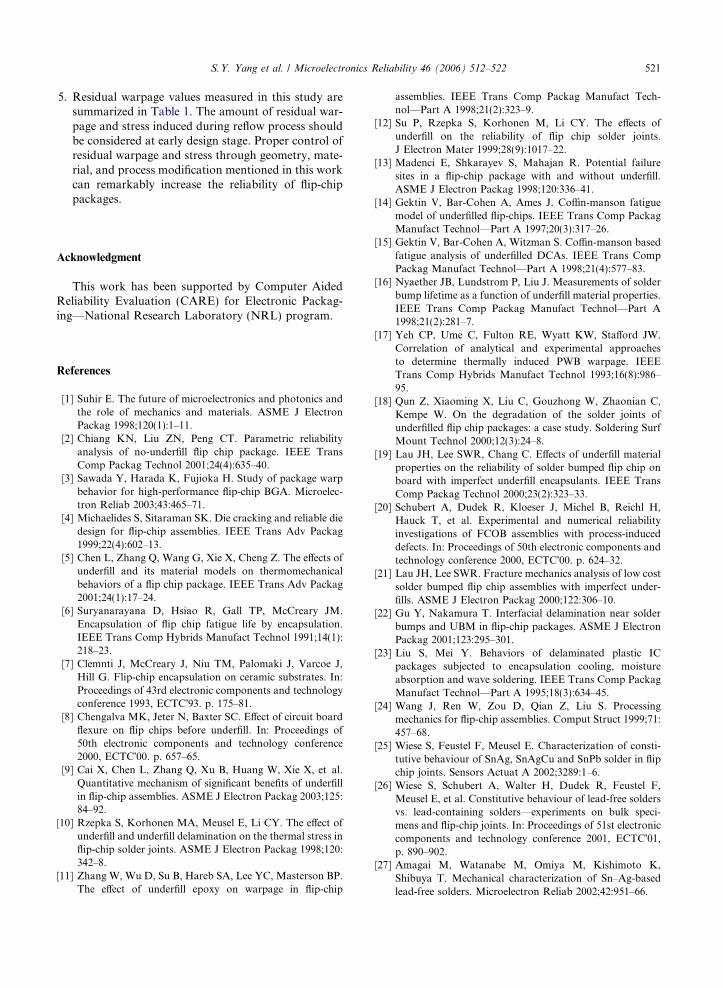
Fig. 1. Flip-chip ass
probe method [32] and laser profilometry [55,56] are welldeveloped and frequently applied methods in electronicpackaging field. Each technique comprises of both mer-its and demerits at the same time, thus, one should care-fully decide considering effectiveness to one�s ownengineering application. Pioneer works of late 1980sand early 1990s, especially on optical methods, are wellsummarized by Suhling [57].
In this work, in-plane Moire interferometry in com-pany with newly developed image processing filter is ap-plied to measure residual warpage of flip-chip aftersolder reflow process. The amount of warpage is rela-tively small, happening to occur between 0 and 10 lm,which is too little to apply conventional geometric Moiremethods. For verification, alternative experimental ap-proaches are performed. Adopting in-plane Moire inter-ferometer and thermal optical chamber, residualwarpage is estimated by in situ measurement of V-dis-placement field while heating the package up to its fullrelaxation. For SAC(Sn/3.0Ag/0.5Cu) which does notrelax even up to 175 �C of heating, shadow Moire tech-nique with fine grating (5 lm pitch) is applied to evalu-ate its residual warpage. In addition, the effect ofmaterial property (SAC vs. SP(Sn/37Pb)) of solders onresidual warpage is emphasized. It is discovered thatresidual warpage and stresses induced during solder re-flow process significantly affects the entire reliability offlip-chip regardless of presence of underfill.
2. Experiments and results
2.1. Flip-chip assembly
The flip-chip package studied in this work is com-posed of silicon chip, C4 solder joints, and PCB sub-strate (Fig. 1). The chip has a side dimension andthickness of 10.0 mm and 0.685 mm, respectively. Single
embly design.

514 S.Y. Yang et al. / Microelectronics Reliability 46 (2006) 512–522
row 144 I/Os are distributed at the peripheral of the chipwith 0.25 mm pitch, 0.12 mm pad size, and 0.095 mmpassivation openings. 19.6 mm2 PCB substrate of0.5 mm thickness is designed with four point probe daisychains so that electrical connection of 16 solders locatedat each corners can be monitored. Electrical resistance ofsolder joints is measured at room temperature in be-tween certain number of cycles. Solder pastes, SP andSAC alloys, are screen-printed on electroless Ni–PUBMs resolving low-cost and simple flip-chip bumping.Five microns of Ni–P layer and 0.08 lm of Au layer areplated on Al pads where solder bumps of 120 lm diam-eter are fabricated subsequently. The solder bumps on Sichip are dipped into a flux and then aligned to the sub-strate using flip-chip bonder. Soldering was performedusing a reflow module on the flip-chip bonder with peaktemperature of 230 �C and 280 �C for SP and SAC,respectively. Reflow of each solder was performed asfollowed processes:
1. Flux activation at 150 �C for 1 min.2. Solder melting at peak temperature for 1 min.3. Air cooling to room temperature.
Finally, flux cleaning is followed in DI (deionized) waterat 60 �C.
2.2. Moire experiment
Moire interferometry is a whole-field in-plane dis-placement optical measurement technique with bothhigh displacement sensitivity and high spatial resolution.It is especially effective for the non-uniform in-planedeformation measurements and has been used in the re-search and development of microelectronic packages tomeasure thermally induced displacement fields.
A thin cross-line diffraction grating is replicated ontothe cross-section of interest and deforms with the sam-
Chip PCB
0.685
10.0
0.5
19.6a
b
Fig. 2. Specimen preparation for Moire experiment: (a) separatereplication at room temperature (23 �C).
ple. Interaction between two coherent laser beams withthe deformed grating produces an interference patternrepresentative of the thermally induced displacementfield. Based on a grating frequency, f of 1200 lines/mm, each interference fringe spacing represents 417 nmrelative displacement difference which explains the defi-nition of sensitivity [38]. Thermally induced deforma-tions can be extracted from the displacement fields bythe following relationship:
Uðx; yÞ ¼ 1
fNxðx; yÞ ð1Þ
V ðx; yÞ ¼ 1
fNyðx; yÞ ð2Þ
where Nx and Ny are the fringe orders in U and V fields,respectively.
In order to measure the residual warpage of chip andPCB after soldering process, bare chip and PCB arecross-sectioned and polished separately until the flat sur-face is guaranteed as in Fig. 2(a). They are polished insuch a way that surface of cross-section is controlledto be shown in Fig. 1. The surface does not include sol-der bumps. Since warpage is a global deformation whichoccurs mainly due to chip and PCB CTE mismatch thepresence of solder in the measured surface would not af-fect the value significantly. After polishing, a 1200 lines/mm cross-line diffraction grating is replicated on thecross-section of interest using TRA-BOND F114 epoxyas shown in Fig. 2(b). The epoxy has Tg of 128 �C andoperation temperature range varies from (�)60 �C to(+)130 �C. The replication is performed at room temper-ature (23 �C) and cured for 24 h. The thickness of epoxyis extremely lower than the specimen. It is controlled tobe below 5 lm. Its modulus is also an order lower thanpackaging materials. Thus the deformation of epoxy isthoroughly confined to that of the specimen. Situationis preferable if temperature exceeds the Tg of theepoxy since the modulus of epoxy is further decreased.
(mm)
Aluminum Grating Mold1200 lines/mm
F114 Epoxy appliedTg=128oC
polishing for chip and PCB; (b) separate diffraction grating
S.Y. Yang et al. / Microelectronics Reliability 46 (2006) 512–522 515
However, epoxy will not reflect the deformation of thespecimen in case the adhesion is lost. The adhesion ofthe epoxy is guaranteed by several pretests. It lastedfor 4000 cycles from (�)50 �C to (+)150 �C.
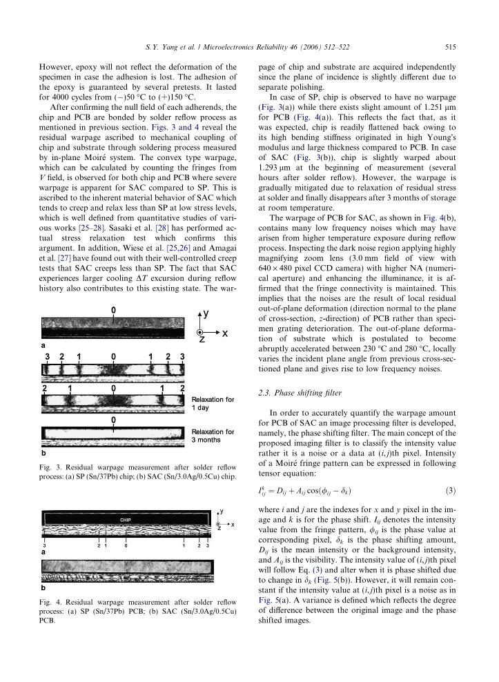
After confirming the null field of each adherends, thechip and PCB are bonded by solder reflow process asmentioned in previous section. Figs. 3 and 4 reveal theresidual warpage ascribed to mechanical coupling ofchip and substrate through soldering process measuredby in-plane Moire system. The convex type warpage,which can be calculated by counting the fringes fromV field, is observed for both chip and PCB where severewarpage is apparent for SAC compared to SP. This isascribed to the inherent material behavior of SAC whichtends to creep and relax less than SP at low stress levels,which is well defined from quantitative studies of vari-ous works [25–28]. Sasaki et al. [28] has performed ac-tual stress relaxation test which confirms thisargument. In addition, Wiese et al. [25,26] and Amagaiet al. [27] have found out with their well-controlled creeptests that SAC creeps less than SP. The fact that SACexperiences larger cooling DT excursion during reflowhistory also contributes to this existing state. The war-
Fig. 3. Residual warpage measurement after solder reflowprocess: (a) SP (Sn/37Pb) chip; (b) SAC (Sn/3.0Ag/0.5Cu) chip.
Fig. 4. Residual warpage measurement after solder reflowprocess: (a) SP (Sn/37Pb) PCB; (b) SAC (Sn/3.0Ag/0.5Cu)PCB.
page of chip and substrate are acquired independentlysince the plane of incidence is slightly different due toseparate polishing.
In case of SP, chip is observed to have no warpage(Fig. 3(a)) while there exists slight amount of 1.251 lmfor PCB (Fig. 4(a)). This reflects the fact that, as itwas expected, chip is readily flattened back owing toits high bending stiffness originated in high Young�smodulus and large thickness compared to PCB. In caseof SAC (Fig. 3(b)), chip is slightly warped about1.293 lm at the beginning of measurement (severalhours after solder reflow). However, the warpage isgradually mitigated due to relaxation of residual stressat solder and finally disappears after 3 months of storageat room temperature.
The warpage of PCB for SAC, as shown in Fig. 4(b),contains many low frequency noises which may havearisen from higher temperature exposure during reflowprocess. Inspecting the dark noise region applying highlymagnifying zoom lens (3.0 mm field of view with640 · 480 pixel CCD camera) with higher NA (numeri-cal aperture) and enhancing the illuminance, it is af-firmed that the fringe connectivity is maintained. Thisimplies that the noises are the result of local residualout-of-plane deformation (direction normal to the planeof cross-section, z-direction) of PCB rather than speci-men grating deterioration. The out-of-plane deforma-tion of substrate which is postulated to becomeabruptly accelerated between 230 �C and 280 �C, locallyvaries the incident plane angle from previous cross-sec-tioned plane and gives rise to low frequency noises.
2.3. Phase shifting filter
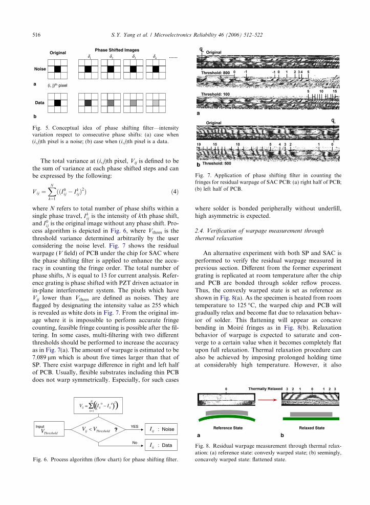
In order to accurately quantify the warpage amountfor PCB of SAC an image processing filter is developed,namely, the phase shifting filter. The main concept of theproposed imaging filter is to classify the intensity valuerather it is a noise or a data at (i, j)th pixel. Intensityof a Moire fringe pattern can be expressed in followingtensor equation:
Ikij ¼ Dij þ Aij cosð/ij � dkÞ ð3Þ
where i and j are the indexes for x and y pixel in the im-age and k is for the phase shift. Iij denotes the intensityvalue from the fringe pattern, /ij is the phase value atcorresponding pixel, dk is the phase shifting amount,Dij is the mean intensity or the background intensity,and Aij is the visibility. The intensity value of (i, j)th pixelwill follow Eq. (3) and alter when it is phase shifted dueto change in dk (Fig. 5(b)). However, it will remain con-stant if the intensity value at (i, j)th pixel is a noise as inFig. 5(a). A variance is defined which reflects the degreeof difference between the original image and the phaseshifted images.
Original
a
b
Phase Shifted Images
Noise
Data
1 2 3 4 ……
(i, j)th pixel
δ δ δ δ
Fig. 5. Conceptual idea of phase shifting filter—intensityvariation respect to consecutive phase shifts: (a) case when(i, j)th pixel is a noise; (b) case when (i, j)th pixel is a data.
Fig. 7. Application of phase shifting filter in counting thefringes for residual warpage of SAC PCB: (a) right half of PCB;(b) left half of PCB.
516 S.Y. Yang et al. / Microelectronics Reliability 46 (2006) 512–522
The total variance at (i, j)th pixel, Vij is defined to bethe sum of variance at each phase shifted steps and canbe expressed by the following:
V ij ¼XN
k¼1
ððI0ij � IkijÞ2Þ ð4Þ
where N refers to total number of phase shifts within asingle phase travel, Ikij is the intensity of kth phase shift,and I0ij is the original image without any phase shift. Pro-cess algorithm is depicted in Fig. 6, where Vthres is thethreshold variance determined arbitrarily by the userconsidering the noise level. Fig. 7 shows the residualwarpage (V field) of PCB under the chip for SAC wherethe phase shifting filter is applied to enhance the accu-racy in counting the fringe order. The total number ofphase shifts, N is equal to 13 for current analysis. Refer-ence grating is phase shifted with PZT driven actuator inin-plane interferometer system. The pixels which haveVij lower than Vthres are defined as noises. They areflagged by designating the intensity value as 255 whichis revealed as white dots in Fig. 7. From the original im-age where it is impossible to perform accurate fringecounting, feasible fringe counting is possible after the fil-tering. In some cases, multi-filtering with two differentthresholds should be performed to increase the accuracyas in Fig. 7(a). The amount of warpage is estimated to be7.089 lm which is about five times larger than that ofSP. There exist warpage difference in right and left halfof PCB. Usually, flexible substrates including thin PCBdoes not warp symmetrically. Especially, for such cases
Thresholdij VV < ?YES
No
ijI : Noise
ijI : Data
Input
ThresholdV
_N
k=
kijijij IIV
1
20Σ ( ))(=
Fig. 6. Process algorithm (flow chart) for phase shifting filter.
where solder is bonded peripherally without underfill,high asymmetric is expected.
2.4. Verification of warpage measurement through
thermal relaxation
An alternative experiment with both SP and SAC isperformed to verify the residual warpage measured inprevious section. Different from the former experimentgrating is replicated at room temperature after the chipand PCB are bonded through solder reflow process.Thus, the convexly warped state is set as reference asshown in Fig. 8(a). As the specimen is heated from roomtemperature to 125 �C, the warped chip and PCB willgradually relax and become flat due to relaxation behav-ior of solder. This flattening will appear as concavebending in Moire fringes as in Fig. 8(b). Relaxationbehavior of warpage is expected to saturate and con-verge to a certain value when it becomes completely flatupon full relaxation. Thermal relaxation procedure canalso be achieved by imposing prolonged holding timeat considerably high temperature. However, it also
Fig. 8. Residual warpage measurement through thermal relax-ation: (a) reference state: convexly warped state; (b) seemingly,concavely warped state: flattened state.

S.Y. Yang et al. / Microelectronics Reliability 46 (2006) 512–522 517
requires certain degree of bending stiffness of the adher-ends to become flat.
In order to resolve deformation behavior during hightemperature condition the Moire system is connected tothe optical environmental chamber (EC1A, Sun Sys-tems) as in Fig. 9. The air inside the chamber must becirculated vigorously to achieve the heating/cooling rateand maintain isothermal condition. Consequently, theenvironmental chamber experiences vibrations, whichare normally transmitted to the specimen. However,vibrations can be tolerated if there is no relative motion,
Fig. 9. Experimental setup for thermal relaxation test: (a) setupfeature; (b) schematic design view (adapted from [45]).
20 40 60 80 100 120-0.5
0.0
0.5
1.0
1.5
2.0
2.5
3.0
3.5
4.0
War
page
(µm
)
Temperature (oC)
FC-P w/o U SAC1 chip 1stFC-P w/o U SAC1 PCB 1stFC-P w/o U SP2 chip 1stFC-P w/o U SP2 PCB 1st
Fig. 10. Residual warpage measure
i.e., if the specimen and the optical system vibrate in uni-son. To fulfill this requirement, the specimen holder isconnected directly to the interferometer and it is essen-tially free from the chamber [45].
In Fig. 10, results clearly reveal that the amount ofresidual warpage is in quite good agreement with thevalues obtained in previous section for SP chip, SPPCB, and SAC chip. However, for SAC PCB, low bend-ing stiffness of PCB as well as low degree of relaxationbehavior of SAC hinder the full relaxation. It failed torelax fully, even at 175 �C with 30 min holding time(Fig. 11). Accurate warpage above 175 �C was unattain-able due to poor spatial resolution caused by high coef-ficient of thermal expansion (CTE), ay of PCB whichresulted in excessive thermal deformation in y-directionas shown in Fig. 11.
2.5. Fine pitch grating shadow Moire
As an alternative solution to quantify the residualwarpage of SAC PCB, a shadow Moire setup is devel-oped. This, non-contact, simple, and relatively low costsetup provides whole-field fringe pattern of out-of-planedisplacement. A Moire pattern is a visual pattern pro-duced by the superposition of two regularly spaced grat-ings that geometrically interfere to create light and darkfringes [35]. The shadow Moire method uses a referencegrating which is placed directly in front of a test objector specimen. The shadow of reference grating on thespecimen, generated from transmitting a collimatedbeam of light through the grating, produces a virtualgrating, termed specimen grating [17]. When the surfaceunder investigation is inclined or curved, shadow Moirefringes are formed by interaction between these two
140
SAC Chip Warpage:
SAC PCB Warpage:More heating required
SP Chip Warpage:0.0 µm
(cf. SAC Chip from Fig.3(b)1.25 µm)
(cf. SP Chip from Fig.3(a)0.0 µm)
SP PCB Warpage:0.938 µm
(cf. SP PCB from Fig.4(a)1.25 µm)
1.334 µm
d by thermal relaxation test.

Fig. 11. Warpage variation measured by thermal relaxation test for SAC PCB up to 175 �C.
D
LCCD Camera
Light Source
ggrating
specimen
αβ
Fig. 12. Typical schematic design for shadow Moire system.
Fig. 13. Feature of shadow Moire setup for this study.
518 S.Y. Yang et al. / Microelectronics Reliability 46 (2006) 512–522
gratings. Fig. 12 is a typical schematic design for shadowMoire system. The governing equation of the out-of-plane displacement can be expressed as the following:
W ¼ gtan aþ tanb
Nz ð5Þ
where g is the grating pitch, Nz is the fringe order, a isthe incident angle, and b is the viewing angle. If theCCD camera and light source are separated by the dis-tance D and located at the identical distance L fromthe grating, by the following relation:
tan aþ tan b ¼ DL
ð6Þ
Eq. (5) is simplified to
W ¼ gLD
Nz ð7Þ
Basic sensitivity,
g ¼ gLD
ð8Þ
which refers to the minimum relative displacement thesystem can optically resolve, is usually set to be 10–100 lm/fringe for shadow Moire. Sensitivity can beenhanced up to sub-micron level by adopting phaseshifting module and imposing related image processingschemes. However, intrinsic non-linearity of phase shift-ers and dependence of image processing on test condi-tions may cause adverse affects to the accuracy andrepeatability of the system. Thus, in this work, opticalsensitivity is elevated by introducing 200 lines/mm(5 lm pitch) quartz glass grating so that the warpageof SAC PCB can be measured which is expected to bearound 7 lm. Fig. 13 shows the shadow Moire setup.Collimated, monochromatic (k = 632.8 nm) laser source
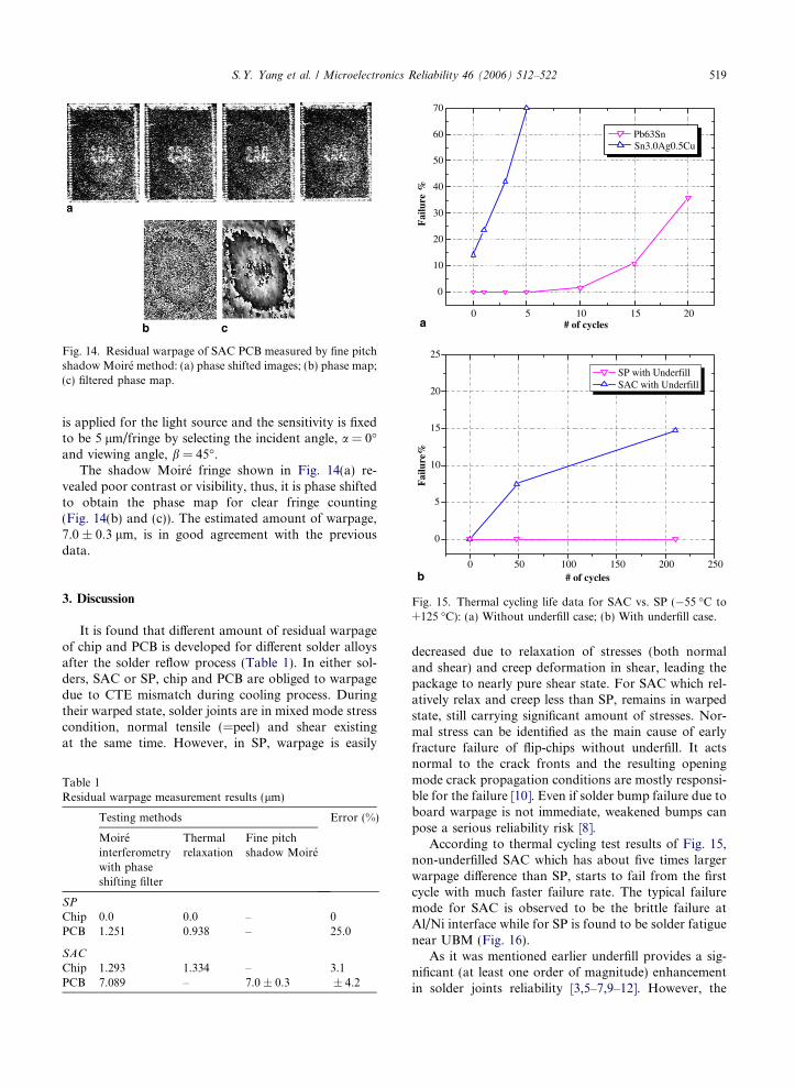
Fig. 14. Residual warpage of SAC PCB measured by fine pitchshadowMoire method: (a) phase shifted images; (b) phase map;(c) filtered phase map.
0 5 10 15 20
0
10
20
30
40
50
60
70
Fai
lure
%
# of cycles
Pb63Sn Sn3.0Ag0.5Cu
0
5
10
15
20
25
Fai
lure
%
SP with Underfill SAC with Underfill
a
S.Y. Yang et al. / Microelectronics Reliability 46 (2006) 512–522 519
is applied for the light source and the sensitivity is fixedto be 5 lm/fringe by selecting the incident angle, a = 0�and viewing angle, b = 45�.
The shadow Moire fringe shown in Fig. 14(a) re-vealed poor contrast or visibility, thus, it is phase shiftedto obtain the phase map for clear fringe counting(Fig. 14(b) and (c)). The estimated amount of warpage,7.0 ± 0.3 lm, is in good agreement with the previousdata.
0 50 100 150 200 250# of cyclesb
Fig. 15. Thermal cycling life data for SAC vs. SP (�55 �C to+125 �C): (a) Without underfill case; (b) With underfill case.
3. Discussion
It is found that different amount of residual warpageof chip and PCB is developed for different solder alloysafter the solder reflow process (Table 1). In either sol-ders, SAC or SP, chip and PCB are obliged to warpagedue to CTE mismatch during cooling process. Duringtheir warped state, solder joints are in mixed mode stresscondition, normal tensile (=peel) and shear existingat the same time. However, in SP, warpage is easily
Table 1Residual warpage measurement results (lm)
Testing methods Error (%)
Moireinterferometrywith phaseshifting filter
Thermalrelaxation
Fine pitchshadow Moire
SP
Chip 0.0 0.0 – 0PCB 1.251 0.938 – 25.0
SAC
Chip 1.293 1.334 – 3.1PCB 7.089 – 7.0 ± 0.3 ± 4.2
decreased due to relaxation of stresses (both normaland shear) and creep deformation in shear, leading thepackage to nearly pure shear state. For SAC which rel-atively relax and creep less than SP, remains in warpedstate, still carrying significant amount of stresses. Nor-mal stress can be identified as the main cause of earlyfracture failure of flip-chips without underfill. It actsnormal to the crack fronts and the resulting openingmode crack propagation conditions are mostly responsi-ble for the failure [10]. Even if solder bump failure due toboard warpage is not immediate, weakened bumps canpose a serious reliability risk [8].
According to thermal cycling test results of Fig. 15,non-underfilled SAC which has about five times largerwarpage difference than SP, starts to fail from the firstcycle with much faster failure rate. The typical failuremode for SAC is observed to be the brittle failure atAl/Ni interface while for SP is found to be solder fatiguenear UBM (Fig. 16).
As it was mentioned earlier underfill provides a sig-nificant (at least one order of magnitude) enhancementin solder joints reliability [3,5–7,9–12]. However, the
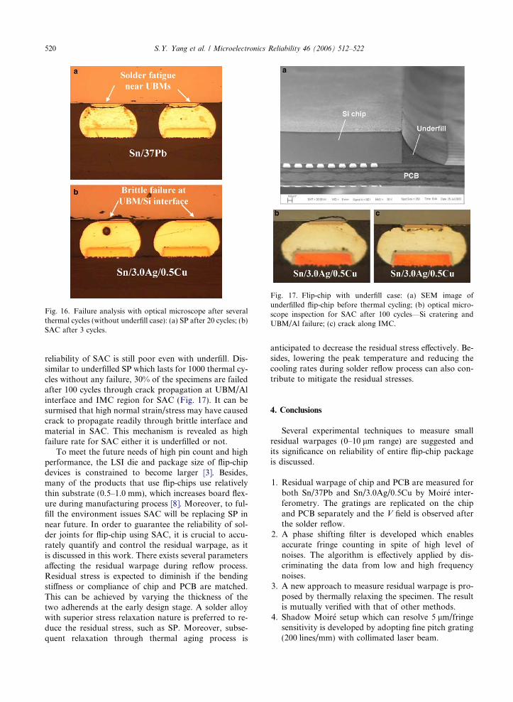
Fig. 16. Failure analysis with optical microscope after severalthermal cycles (without underfill case): (a) SP after 20 cycles; (b)SAC after 3 cycles.
Fig. 17. Flip-chip with underfill case: (a) SEM image ofunderfilled flip-chip before thermal cycling; (b) optical micro-scope inspection for SAC after 100 cycles—Si cratering andUBM/Al failure; (c) crack along IMC.
520 S.Y. Yang et al. / Microelectronics Reliability 46 (2006) 512–522
reliability of SAC is still poor even with underfill. Dis-similar to underfilled SP which lasts for 1000 thermal cy-cles without any failure, 30% of the specimens are failedafter 100 cycles through crack propagation at UBM/Alinterface and IMC region for SAC (Fig. 17). It can besurmised that high normal strain/stress may have causedcrack to propagate readily through brittle interface andmaterial in SAC. This mechanism is revealed as highfailure rate for SAC either it is underfilled or not.
To meet the future needs of high pin count and highperformance, the LSI die and package size of flip-chipdevices is constrained to become larger [3]. Besides,many of the products that use flip-chips use relativelythin substrate (0.5–1.0 mm), which increases board flex-ure during manufacturing process [8]. Moreover, to ful-fill the environment issues SAC will be replacing SP innear future. In order to guarantee the reliability of sol-der joints for flip-chip using SAC, it is crucial to accu-rately quantify and control the residual warpage, as itis discussed in this work. There exists several parametersaffecting the residual warpage during reflow process.Residual stress is expected to diminish if the bendingstiffness or compliance of chip and PCB are matched.This can be achieved by varying the thickness of thetwo adherends at the early design stage. A solder alloywith superior stress relaxation nature is preferred to re-duce the residual stress, such as SP. Moreover, subse-quent relaxation through thermal aging process is
anticipated to decrease the residual stress effectively. Be-sides, lowering the peak temperature and reducing thecooling rates during solder reflow process can also con-tribute to mitigate the residual stresses.
4. Conclusions
Several experimental techniques to measure smallresidual warpages (0–10 lm range) are suggested andits significance on reliability of entire flip-chip packageis discussed.
1. Residual warpage of chip and PCB are measured forboth Sn/37Pb and Sn/3.0Ag/0.5Cu by Moire inter-ferometry. The gratings are replicated on the chipand PCB separately and the V field is observed afterthe solder reflow.
2. A phase shifting filter is developed which enablesaccurate fringe counting in spite of high level ofnoises. The algorithm is effectively applied by dis-criminating the data from low and high frequencynoises.
3. A new approach to measure residual warpage is pro-posed by thermally relaxing the specimen. The resultis mutually verified with that of other methods.
4. Shadow Moire setup which can resolve 5 lm/fringesensitivity is developed by adopting fine pitch grating(200 lines/mm) with collimated laser beam.
S.Y. Yang et al. / Microelectronics Reliability 46 (2006) 512–522 521
5. Residual warpage values measured in this study aresummarized in Table 1. The amount of residual war-page and stress induced during reflow process shouldbe considered at early design stage. Proper control ofresidual warpage and stress through geometry, mate-rial, and process modification mentioned in this workcan remarkably increase the reliability of flip-chippackages.
Acknowledgment
This work has been supported by Computer AidedReliability Evaluation (CARE) for Electronic Packag-ing—National Research Laboratory (NRL) program.
References
[1] Suhir E. The future of microelectronics and photonics andthe role of mechanics and materials. ASME J ElectronPackag 1998;120(1):1–11.
[2] Chiang KN, Liu ZN, Peng CT. Parametric reliabilityanalysis of no-underfill flip chip package. IEEE TransComp Packag Technol 2001;24(4):635–40.
[3] Sawada Y, Harada K, Fujioka H. Study of package warpbehavior for high-performance flip-chip BGA. Microelec-tron Reliab 2003;43:465–71.
[4] Michaelides S, Sitaraman SK. Die cracking and reliable diedesign for flip-chip assemblies. IEEE Trans Adv Packag1999;22(4):602–13.
[5] Chen L, Zhang Q, Wang G, Xie X, Cheng Z. The effects ofunderfill and its material models on thermomechanicalbehaviors of a flip chip package. IEEE Trans Adv Packag2001;24(1):17–24.
[6] Suryanarayana D, Hsiao R, Gall TP, McCreary JM.Encapsulation of flip chip fatigue life by encapsulation.IEEE Trans Comp Hybrids Manufact Technol 1991;14(1):218–23.
[7] Clemnti J, McCreary J, Niu TM, Palomaki J, Varcoe J,Hill G. Flip-chip encapsulation on ceramic substrates. In:Proceedings of 43rd electronic components and technologyconference 1993, ECTC�93. p. 175–81.
[8] Chengalva MK, Jeter N, Baxter SC. Effect of circuit boardflexure on flip chips before underfill. In: Proceedings of50th electronic components and technology conference2000, ECTC�00. p. 657–65.
[9] Cai X, Chen L, Zhang Q, Xu B, Huang W, Xie X, et al.Quantitative mechanism of significant benefits of underfillin flip-chip assemblies. ASME J Electron Packag 2003;125:84–92.
[10] Rzepka S, Korhonen MA, Meusel E, Li CY. The effect ofunderfill and underfill delamination on the thermal stress inflip-chip solder joints. ASME J Electron Packag 1998;120:342–8.
[11] Zhang W, Wu D, Su B, Hareb SA, Lee YC, Masterson BP.The effect of underfill epoxy on warpage in flip-chip
assemblies. IEEE Trans Comp Packag Manufact Tech-nol—Part A 1998;21(2):323–9.
[12] Su P, Rzepka S, Korhonen M, Li CY. The effects ofunderfill on the reliability of flip chip solder joints.J Electron Mater 1999;28(9):1017–22.
[13] Madenci E, Shkarayev S, Mahajan R. Potential failuresites in a flip-chip package with and without underfill.ASME J Electron Packag 1998;120:336–41.
[14] Gektin V, Bar-Cohen A, Ames J. Coffin-manson fatiguemodel of underfilled flip-chips. IEEE Trans Comp PackagManufact Technol—Part A 1997;20(3):317–26.
[15] Gektin V, Bar-Cohen A, Witzman S. Coffin-manson basedfatigue analysis of underfilled DCAs. IEEE Trans CompPackag Manufact Technol—Part A 1998;21(4):577–83.
[16] Nyaether JB, Lundstrom P, Liu J. Measurements of solderbump lifetime as a function of underfill material properties.IEEE Trans Comp Packag Manufact Technol—Part A1998;21(2):281–7.
[17] Yeh CP, Ume C, Fulton RE, Wyatt KW, Stafford JW.Correlation of analytical and experimental approachesto determine thermally induced PWB warpage. IEEETrans Comp Hybrids Manufact Technol 1993;16(8):986–95.
[18] Qun Z, Xiaoming X, Liu C, Gouzhong W, Zhaonian C,Kempe W. On the degradation of the solder joints ofunderfilled flip chip packages: a case study. Soldering SurfMount Technol 2000;12(3):24–8.
[19] Lau JH, Lee SWR, Chang C. Effects of underfill materialproperties on the reliability of solder bumped flip chip onboard with imperfect underfill encapsulants. IEEE TransComp Packag Technol 2000;23(2):323–33.
[20] Schubert A, Dudek R, Kloeser J, Michel B, Reichl H,Hauck T, et al. Experimental and numerical reliabilityinvestigations of FCOB assemblies with process-induceddefects. In: Proceedings of 50th electronic components andtechnology conference 2000, ECTC�00. p. 624–32.
[21] Lau JH, Lee SWR. Fracture mechanics analysis of low costsolder bumped flip chip assemblies with imperfect under-fills. ASME J Electron Packag 2000;122:306–10.
[22] Gu Y, Nakamura T. Interfacial delamination near solderbumps and UBM in flip-chip packages. ASME J ElectronPackag 2001;123:295–301.
[23] Liu S, Mei Y. Behaviors of delaminated plastic ICpackages subjected to encapsulation cooling, moistureabsorption and wave soldering. IEEE Trans Comp PackagManufact Technol—Part A 1995;18(3):634–45.
[24] Wang J, Ren W, Zou D, Qian Z, Liu S. Processingmechanics for flip-chip assemblies. Comput Struct 1999;71:457–68.
[25] Wiese S, Feustel F, Meusel E. Characterization of consti-tutive behaviour of SnAg, SnAgCu and SnPb solder in flipchip joints. Sensors Actuat A 2002;3289:1–6.
[26] Wiese S, Schubert A, Walter H, Dudek R, Feustel F,Meusel E, et al. Constitutive behaviour of lead-free soldersvs. lead-containing solders—experiments on bulk speci-mens and flip-chip joints. In: Proceedings of 51st electroniccomponents and technology conference 2001, ECTC�01,p. 890–902.
[27] Amagai M, Watanabe M, Omiya M, Kishimoto K,Shibuya T. Mechanical characterization of Sn–Ag-basedlead-free solders. Microelectron Reliab 2002;42:951–66.

522 S.Y. Yang et al. / Microelectronics Reliability 46 (2006) 512–522
[28] Sasaki K, Yanagimoto A, Ishikawa H. Effect of lead andlead-free solders on bend of substrate. In: Proceedings ofadvanced technology in experimental mechanics 2003,ATEM�03, OS10W0040.
[29] Liu S, Mei Y, Wu TY. Bimaterial interfacial crack growthas a function of mode-mixity. IEEE Trans Comp PackagManufact Technol—Part A 1995;18(3):618–26.
[30] Liu S, Zhu JS, Hu JM, Pao YH. Investigation of crackpropagation in ceramic/conductive adhesive/glass systems.IEEE Trans Comp Packag Manufact Technol—Part A1995;18(3):627–33.
[31] Wang J, Qian Z, Liu S. Process induced stresses of a flip-chip packag by sequential processing modeling technique.ASME J Electron Packag 1998;120:309–13.
[32] Yeung DTS, Yuen MMF. Warpage of plastic IC packagesas a function of processing conditions. ASME J ElectronPackag 2001;123:268–72.
[33] Palaniappan P, Baldwin DF. In process stress analysis offlip-chip assemblies during underfill cure. MicroelectronReliab 2000;40:1181–90.
[34] Driel WD, Zhang GQ, Janssen JHJ, Ernst LJ, Su F, ChianKS, et al. Prediction and verification of process inducedwarpage of electronic packages. Microelectron Reliab2003;43:765–74.
[35] Polsky Y, Sutherlin W, Ume IC. A comparison of PWBwarpage due to simulated infrared and wave solderingprocesses. IEEE Trans Electron Packag Manufact 2000;23(3):191–9.
[36] Stiteler MR, Ume IC, Leutz B. In-process board warpagemeasurement in a lab scale wave soldering oven. IEEETrans Comp Packag Manufact Technol—Part A 1996;19(4):562–9.
[37] Chien CH, Chen YC, Chiou YT, Chen T, Hsieh CC, YanJJ, et al. Influences of the moisture absorption on PBGApackage�s warpage during IR reflow process. Microelec-tron Reliab 2003;43:131–9.
[38] Post D, Han B, Ifju P. High sensitivity Moire. NewYork: Spring-Verlag; 1994.
[39] Karalekas D, Aggelopoulos A. Study of shrinkage strainsin stereolithography cured acrylic photopolymer resin.J Mater Process Technol 2003;136:146–50.
[40] Lin TY, Njoman B, Crouthamel D, Chua KH, Teo SY,Ma YY. The impact of moisture in mold compoundperforms on the warpage of PBGA packages. Microelec-tron Reliab 2004;44:603–9.
[41] Ding H, Powell RE, Hanna CR, Ume IC. Warpagemeasurement comparison using shadow Moire and pro-jection Moire methods. In: Proceedings of 52nd electroniccomponents and technology conference 2002, ECTC�02.p. 176–82.
[42] Bhattacharya SK, Ume IC, Dang AXH. Warpage mea-surement of large area multitilted silicon substrates atvarious processing conditions. IEEE Trans Comp PackagTechnol 2000;23(3):497–504.
[43] Voloshin AS, Tsao PH, Pearson RA. In situ evaluation ofresidual stresses in an organic die-attach adhesive. ASME JElectron Packag 1998;120:314–8.
[44] Stout EA, Sottos NR, Skipor AF. Mechanical character-ization of plastic ball grid array package flexure using
Moire inteferometry. IEEE Trans Adv Packag 2000;23(4):637–45.
[45] Cho SM, Cho SY, Han B. Observing real-time thermaldeformations in electronic packaging. Exp Tech 2002;26(3):25–9.
[46] Guo Y, Woychik CG. Thermal strain measurement ofsolder joints in second level interconnections using Moireinterferometry. ASME J Electron Packag 1992;114(1):88–92.
[47] Han B. Thermal stresses in microelectronics subassemblies:quantitative characterization using photomechanics meth-ods. J Thermal Stresses 2003;26(6):1–16.
[48] KwonWS, Yang SY, Lee SB, Paik KW. The effect of Tg onthermo-mechanical deformation and reliability of adhesiveflip chip assemblies during temperature cycling. In: Pro-ceedings of 54th electronic components and technologyconference 2004, ECTC�04. p. 1731–7.
[49] Yang SY, Lee SB, Kwon WS, Paik KW. Analyticalapproach to evaluate shear stress in flip chip interconnec-tion using NCA/ACF. In: Proceedings of 4th internationalsymposium on electronic materials and packaging 2002,EMAP2002. p. 415–20.
[50] Wen Y, Basaran C. An analytical model for thermal stressanalysis of multi-layered microelectronics packaging. MechMater 2004;36:369–85.
[51] Guo Y, Liu S. Development in optical methods forreliability analysis in electronic packaging applications.ASME J Electron Packag 1998;120:186–93.
[52] Han B, Guo Y, Lim CK, Caletka D. Verificationof numerical models used in microelectronics packag-ing design by interferometric displacement measure-ment methods. ASME J Electron Packag 1996;118:157–63.
[53] Verma K, Park SB, Han B. On the design parameters offlip-chip PBGA package assembly for optimum solder ballreliability. IEEE Trans Comp Packag Technol 2001;24(2):300–7.
[54] Verma K, Han B. Warpage measurement on dielectricrough surfaces of microelectronics devices by far infraredfizeau interferometry. ASME J Electron Packag 2000;122:227–32.
[55] Du Y, Zhao JH, Ho P. An optical method for measuringthe two-dimensional surface curvatures of electronic pack-ages during thermal cycling. ASME J Electron Packag2001;123:196–9.
[56] Kim JS, Paik KW, Seo HS. A quantitative analysis of thestress relaxation effect of thermoplastics in multilayersubstrates. IEEE Trans Adv Packag 1999;22(4):638–41.
[57] Suhling JC, Lin ST. Application of optical methods toelectronic packaging. Applicat Exp Mech Electron PackagASME 1995;EEP-13/AMD-214:39–45.
[58] Miyake K, Yoshida T, Baik HG, Park SW. Viscoelasticwarpage analysis of surface mount package. ASME JElectron Packag 2001;123:101–4.
[59] Kong JWY, Kim JK, Yuen MMF. Warpage in plasticpackages: effects of process conditions, geometry andmaterials. IEEE Trans Electron Packag Manufact2003;26(3):245–52.