software engineering for embedded systems || optimizing embedded software for power
TRANSCRIPT

CHAPTER 13
Optimizing Embedded Software for PowerRobert Oshana
Chapter Outline
Introduction 368
Understanding power consumption 369Basics of power consumption 369
Static vs. dynamic power consumption 370
Static power consumption 370
Dynamic power consumption 371
Maximum, average, worst-case, and typical power 371
Measuring power consumption 372Measuring power using an ammeter 372
Measuring power using a hall sensor type IC 373
VRMs (voltage regulator module power supply ICs) 374
Static power measurement 375
Dynamic power measurement 375
Profiling your application’s power consumption 376
Minimizing power consumption 377Hardware support 378
Low-power modes (introduction to devices) 378
Example low-power modes 380
Texas Instruments C6000 low-power modes 381
Clock and voltage control 382
Considerations and usage examples of low-power modes 383
Low-power example 383
Optimizing data flow 388Reducing power consumption for memory accesses 388
DDR overview 389
DDR data flow optimization for power 392
Optimizing power by timing 393
Optimizing with interleaving 394
Optimizing memory software data organization 394
Optimizing general DDR configuration 394
Optimizing DDR burst accesses 394
SRAM and cache data flow optimization for power 395SRAM (all memory) and code size 396
SRAM power consumption and parallelization 397
367Software Engineering for Embedded Systems.
DOI: http://dx.doi.org/10.1016/B978-0-12-415917-4.00013-X
© 2013 Elsevier Inc. All rights reserved.
Data transitions and power consumption 397
Cache utilization and SoC memory layout 397
Explanation of locality 398
Explanation of set-associativity 399
Memory layout for cache 401
Write-back vs. write-through caches 401
Cache coherency functions 402
Compiler cache optimizations 403
Peripheral/communication utilization 403DMA of data vs. CPU 405
Coprocessors 406
System bus configuration 406
Peripheral speed grades and bus width 407
Peripheral to core communication 407
Polling 407
Time-based processing 408
Interrupt processing 408
Algorithmic 408Compiler optimization levels 408
Instruction packing 409
Loop unrolling revisited 409
Software pipelining 410
Eliminating recursion 412
Reducing accuracy 415
Low-power code sequences and data patterns 416
Summary and closing remarks 416
Introduction
One of the most important considerations in the product lifecycle of an embedded project is
to understand and optimize the power consumption of the device. Power consumption is
highly visible for hand-held devices which require battery power to be able to guarantee
certain minimum usage/idle times between recharging. Other embedded applications, such
as medical equipment, test, measurement, media, and wireless base stations, are very
sensitive to power as well � due to the need to manage the heat dissipation of increasingly
powerful processors, power supply cost, and energy consumption cost � so the fact is that
power consumption cannot be overlooked.
The responsibility for setting and keeping power requirements often falls on the shoulders
of hardware designers, but the software programmer has the ability to provide a large
contribution to power optimization. Often, the impact that the software engineer has on
influencing the power consumption of a device is overlooked or underestimated.
368 Chapter 13

The goal of this section is to discuss how software can be used to optimize power
consumption, starting with the basics of what power consumption consists of, how to
properly measure power consumption, and then moving on to techniques for minimizing
power consumption in software at the algorithmic level, hardware level, and data-flow
level. This will include demonstrations of the various techniques and explanations of both
how and why certain methods are effective at reducing power so the reader can take and
apply this work to their application right away.
Understanding power consumption
Basics of power consumption
In general, when power consumption is discussed, the four main factors discussed for a
device are the application, the frequency, the voltage and the process technology, so we
need to understand why exactly it is that these factors are so important.
The application is highly important, so much so that the power profile for two hand-held
devices could differ to the point of making power optimization strategies the complete
opposite. While we will be explaining more about power optimization strategies later on,
the basic idea is clear enough to introduce in this section.
Take for example a portable media player vs. a cellular phone. The portable media player
needs to be able to run at 100% usage for a long period of time to display video (full-length
movies), audio, etc. We will discuss this later, but the general power-consumption profile
for this sort of device would have to focus on algorithmic and data flow power optimization
more than on efficient usage of low-power modes.
Compare this to the cellular phone, which spends most of its time in an idle state, and
during call time the user only talks for a relatively small percentage of the time. For this
small percentage of time, the processor may be heavily loaded, performing encode/decode
of voice and transmit/receive data. For the remainder of the call time, the phone is not so
heavily tasked, performing procedures such as sending heartbeat packets to the cellular
network and providing “comfort noise” to the user to let the user know the phone is still
connected during silence. For this sort of profile, power optimization would be focused first
on maximizing processor sleep states to save as much power as possible, and then on data
flow/algorithmic approaches.
In the case of process technology, the current cutting-edge embedded cores are based on
45 nm and in the near future 28 nm technology, a decrease in size from its predecessor, the
65 nm technology. What this smaller process technology provides is a smaller transistor.
Smaller transistors consume less power and produce less heat, so are clearly advantageous
compared with their predecessors.
Optimizing Embedded Software for Power 369

Smaller process technology also generally enables higher clock frequencies, which is
clearly a plus, providing more processing capability, but higher frequency, along with
higher voltage, comes at the cost of higher power draw. Voltage is the most obvious of
these, as we learned in physics (and EE101), power is the product of voltage times current.
So if a device requires a large voltage supply, power consumption increase is a fact of life.
While staying on the subject of P5V�I, the frequency is also directly part of this equation
because current is a direct result of the clock rate. Another thing we learned in physics and
EE101: when voltage is applied across a capacitor, current will flow from the voltage
source to the capacitor until the capacitor has reached an equivalent potential. While this is
an over-simplification, we can imagine that the clock network in a core consumes power in
such a fashion. Thus at every clock edge, when the potential changes, current flows through
the device until it reaches the next steady state. The faster the clock is switching, the more
current is flowing, therefore faster clocking implies more power consumed by the
embedded processor. Depending on the device, the clock circuit is responsible for
consuming between 50% and 90% of dynamic device power, so controlling clocks is a
theme that will be covered very heavily here.
Static vs. dynamic power consumption
Total power consumption consists of two types of power: dynamic and static (also known
as static leakage) consumption, so total device power is calculated as:
Ptotal5PDynamic1PStatic
As we have just discussed, clock transitions are a large portion of the dynamic
consumption, but what is this “dynamic consumption”? Basically, in software we have
control over dynamic consumption, but we do not have control over static consumption.
Static power consumption
Leakage consumption is the power that a device consumes independent of any activity or
task the core is running, because even in a steady state there is a low “leakage” current path
(via transistor tunneling current, reverse diode leakage, etc.) from the device’s Vin to
ground. The only factors that affect the leakage consumption are supply voltage,
temperature, and process.
We have already discussed voltage and process in the introduction. In terms of temperature,
it is fairly intuitive to understand why heat increases leakage current. Heat increases the
mobility of electron carriers, which will lead to an increase in electron flow, causing greater
static power consumption. As the focus of this chapter is software, this will be the end of
static power consumption theory.
370 Chapter 13

Dynamic power consumption
The dynamic consumption of the embedded processor includes the power consumed by the
device actively using the cores, core subsystems, peripherals such as DMA, I/O (radio,
Ethernet, PCIe, CMOS camera), memories, and PLLs and clocks. At the low level, this can
be translated to say that dynamic power is the power consumed by switching transistors
which are charging and discharging capacitances.
Dynamic power increases as we use more elements of the system, more cores, more
arithmetic units, more memories, higher clock rates, or anything that could possibly
increase the amount of transistors switching, or the speed at which they are switching. The
dynamic consumption is independent of temperature, but still depends on voltage supply
levels.
Maximum, average, worst-case, and typical power
When measuring power, or determining power usage for a system, there are four main types
of power that need to be considered: maximum power, average power, worst-case power
consumption, and typical power consumption.
Maximum and average power are general terms, used to describe the power measurement
itself more than the effect of software or other variables on a device’s power consumption.
Simply stated, maximum power is the highest instantaneous power reading measured over a
period of time. This sort of measurement is useful to show the amount of decoupling
capacitance required by a device to maintain a decent level of signal integrity (required for
reliable operation).
Average power is intuitive at this point: technically the amount of energy consumed in a
time period, divided by that time (power readings averaged over time). Engineers do this by
calculating the average current consumed over time and use that to find power. Average
power readings are what we are focusing on optimizing as this is the determining factor for
how much power a battery or power supply must be able to provide for a processor to
perform an application over time, and this also used to understand the heat profile of the
device.
Both worst case and typical power numbers are based on average power measurement.
Worst-case power, or the worst-case power profile, describes the amount of average power
a device will consume at 100% usage over a given period. One hundred percent usage
refers to the processer utilizing the maximum number of available processing units (data
and address generation blocks in the core, accelerators, bit masking, etc.), memories, and
peripherals simultaneously. This may be simulated by putting the cores in an infinite loop
of performing six or more instructions per cycle (depending on the available processing
Optimizing Embedded Software for Power 371

units in the core) while having multiple DMA channels continuously reading from and
writing to memory, and peripherals constantly sending and receiving data. Worst-case
power numbers are used by the system architect or board designer in order to provide
adequate power supply to guarantee functionality under all worst-case conditions.
In a real system, a device will rarely if ever draw the worst-case power, as applications do
not use all the processing elements, memory, and I/O for long periods of time, if at all. In
general, a device provides many different I/O peripherals, though only a portion of them are
needed, and the device cores may only need to perform heavy computation for small
portions of time, accessing just a portion of memory. Typical power consumption then may
be based on the assumed “general use case” example application that may use anywhere
from 50% to 70% of the processor’s available hardware components at a time. This is a
major aspect of software applications that we are going to be taking advantage of in order
to optimize power consumption.
In this section we have explained the differences of static vs. dynamic power, maximum
vs. average power, process effect on power, and core and processing power effect on
power. Now that the basics of what makes power consumption are covered, we will
discuss power consumption measurement before going into detail about power
optimization techniques.
Measuring power consumption
Now that background, theory, and vocabulary have been covered, we will move on to
taking power measurements. We will discuss the types of measurements used to get
different types of power readings (such as reading static vs. dynamic power), and use these
methods in order to test optimization methods used later in the text.
Measuring power is hardware dependent: some embedded processors provide internal
measurement capabilities; processor manufacturers may also provide “power calculators”
which give some power information; there are a number of power supply controller ICs
which provide different forms of power measurement capabilities; some power supply
controllers called VRMs (voltage regulator modules) have these capabilities internal to
them to be read over peripheral interfaces; and finally, there is the old-fashioned method of
connecting an ammeter in series to the core power supply.
Measuring power using an ammeter
The “old-fashioned” method is to measure power via the use of an external power supply
connected in series to the positive terminal of an ammeter, which connects via the negative
connector to the DSP device power input, as shown in Figure 13.1.
372 Chapter 13

Note that there are three different set-ups shown in Figure 13.1, which are all for a
single processor. This is due to the fact that processor power input is isolated, generally
between cores (possibly multiple supplies), peripherals, and memories. This is done by
design in hardware as different components of a device have different voltage
requirements, and this is useful to isolate (and eventually optimize) the power profile of
individual components.
In order to properly measure power consumption, the power to each component
must be properly isolated, which in some cases may require board modification,
specific jumper settings, etc. The most ideal situation is to be able to connect the
external supply/ammeter combination as close as possible to the processor power input
pins.
Alternatively, one may measure the voltage drop across a (shunt) resister which is in series
with the power supply and the processor power pins. By measuring the voltage drop across
the resistor, current is found simply by calculating I5V/R.
Measuring power using a hall sensor type IC
In order to simplify efficient power measurement, many embedded vendors are building
boards that use a Hall-effect-based sensor. When a Hall sensor is placed on a board in the
current path to the device’s power supply, it generates a voltage equivalent to the current
times some coefficient with an offset. In the case of Freescale’s MSC8144 DSP Application
Development System board, an Allegro ACS0704 Hall sensor is provided on the board,
which enables such measurement. With this board, the user can simply place a scope to the
board, and view the voltage signal over time, and use this to calculate average power using
Allegro’s current to voltage graph, shown in Figure 13.2.
A
Power Supply
+ - -
DSPPeripheral
Supply
A
Power Supply
+ - -
DSPMemorySupply
A
Power Supply
+ - -
DSP CoreSupply
Figure 13.1:Measuring power via ammeters.
Optimizing Embedded Software for Power 373

Using Figure 13.2, we can calculate input current to a device based on measuring potential
across Vout as:
I5 ðVout2 2:5Þ�10A
VRMs (voltage regulator module power supply ICs)
Finally, some VRMs (power supply controller ICs), which are used to split a large
input voltage into a number of smaller ones to supply individual sources at varying
potentials, measure current/power consumption and store the values in registers to be
read by the user. Measuring current via the VRM requires no equipment, but this
sometimes comes at the cost of accuracy and real-time measurement. For example, the
PowerOne ZM7100 series VRM (also used on the MSC8144ADS) provides current
readings for each supply, but the current readings are updated once every 0.5 to 1
seconds, and the reading accuracy is of the order of B20%, so instantaneous reading
for maximum power is not possible, and fine tuning and optimization may not be
possible using such devices.
In addition to deciding a specific method for measuring power in general, different
methods exist to measure dynamic power versus static leakage consumption. The static
leakage consumption data is useful in order to have a floor for our low-power
–20 –15 –10 –5 0 5 10 15 20Ip (A)
0
0.5
1.0
1.5
2.0
2.5
3.0
3.5
4.0
4.5
5.0
Output Voltage versus Primary Current
VCC= 5 V
–40–202585
150
oC
Figure 13.2:Hall effect IC voltage to current graph (www.allegromicro.com/en/Products/Part. . ./0704/
0704-015.pdf).
374 Chapter 13
expectations, and to understand how much power the actual application is pulling versus
what the device will pull in idle. We can then subtract that from the total power
consumption we measure in order to determine the dynamic consumption the processor
is pulling, and work to minimize that. There are various tools available in the industry
to help in this area.
Static power measurement
Leakage consumption on a processor can usually be measured while the device is placed
in a low-power mode, assuming that the mode shuts down clocks to all of the core
subsystems and peripherals. If the clocks are not shut down in low-power mode, the
PLLs should be bypassed, and then the input clock should be shut down, thus shutting
down all clocks and eliminating clock and PLL power consumption from the static
leakage measurement.
Additionally, static leakage should be measured at varying temperatures since leakage
varies based on temperature. Creating a set of static measurements based on
temperature (and voltage) provides valuable reference points for determining how
much dynamic power an application is actually consuming at these temperature/voltage
points.
Dynamic power measurement
The power measurements should separate the contribution of each major module in the
device to give the engineer information about what effect a specific configuration will
have on a system’s power consumption. As noted above, dynamic power is found
simply by measuring the total power (at a given temperature) and then subtracting the
leakage consumption for that given temperature using the initial static measurements
from above.
Initial dynamic measurement tests include running sleep-state tests, debug-state tests, and a
NOP test. Sleep-state and debug-state tests will give the user insight into the cost of
enabling certain clocks in the system. A NOP test, as in a loop of NOP commands, will
provide a baseline dynamic reading for your core’s consumption when mainly using the
fetch unit of the device, but no arithmetic units, address generation, bit mask, memory
management, etc.
When comparing specific software power optimization techniques, we compare the before
and after power consumption numbers of each technique in order to determine the effect of
that technique.
Optimizing Embedded Software for Power 375
Profiling your application’s power consumption
Before optimizing an application for power, the programmer should get a baseline power
reading of the section of code being optimized. This provides a reference point for
measuring optimizations, and also ensures that the alterations to code do in fact decrease
total power, and not the opposite. In order to do this, the programmer needs to generate a
sample power test which acts as a snapshot of the code segment being tested.
This power test-case generation can be done by profiling code performance using a high-
end profiler to gain some base understanding of the percentage of processing elements and
memory used. We can demonstrate this by creating a new project in a standard tools IDE
(there are many available) with the profiler enabled, then compiling, and running the
project. The application will run from start to finish, at which point the user may select a
profiler view and get any number of statistics.
Using relevant data such as the percentage of ALUs used, AGUs used, code hot-spots, and
knowledge of memories being accessed, we can get a general idea of where our code will
spend the most time (and consume the most power). We can use this to generate a basic
performance test which runs in an infinite loop, enabling us to profile the average “typical”
power of an important code segment.
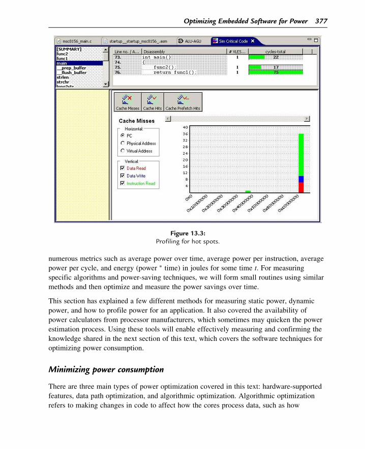
As an example, using two main functions: func1 and func2. Profiling the example code, we
can see from the Figure 13.3 that the vast majority of cycles are consumed by the func1
routine. This routine is located in M2 memory and reads data from cacheable M3 memory
(meaning possible causing write back accesses to L2 and L1 cache). By using the profiler
(as per Figure 13.4), information regarding the percentage ALU and percentage AGU can
be extracted. We can effectively simulate this by turning the code into an infinite loop,
adjusting the I/O, and compiling at the same optimization level, and verifying that we see
the same performance breakdown. Another option would be to write a sample test in
assembly code to force certain ALU/AGU usage models to match our profile, though this is
not as precise and makes testing of individual optimizations more difficult.
We can then set a break point, re-run our application, and confirm that the device usage
profile is in line with our original code. If not, we can adjust the compiler optimization
level or our code until it matches the original application.
This method is quick and effective for measuring core power consumption for various loads
and, if we mirrored the original application by properly using the profiler, this should
account for stalls and other pipeline issues as the profiler provides information on total
cycle count as well as instruction and VLES utilization. By having the infinite loop, testing
is much easier as we are simply comparing steady-state current readings of optimized and
non-optimized code in the hope of getting lower numbers. We can use this to measure
376 Chapter 13
numerous metrics such as average power over time, average power per instruction, average
power per cycle, and energy (power � time) in joules for some time t. For measuring
specific algorithms and power-saving techniques, we will form small routines using similar
methods and then optimize and measure the power savings over time.
This section has explained a few different methods for measuring static power, dynamic
power, and how to profile power for an application. It also covered the availability of
power calculators from processor manufacturers, which sometimes may quicken the power
estimation process. Using these tools will enable effectively measuring and confirming the
knowledge shared in the next section of this text, which covers the software techniques for
optimizing power consumption.
Minimizing power consumption
There are three main types of power optimization covered in this text: hardware-supported
features, data path optimization, and algorithmic optimization. Algorithmic optimization
refers to making changes in code to affect how the cores process data, such as how
Figure 13.3:Profiling for hot spots.
Optimizing Embedded Software for Power 377

instructions or loops are handled, whereas hardware optimization, as discussed here, focuses
more on how to optimize clock control and power features provided in hardware. Data flow
optimization focuses on working to minimize the power cost of utilizing different
memories, buses, and peripherals where data can be stored or transmitted by taking
advantage of relevant features and concepts.
Hardware support
Low-power modes (introduction to devices)
DSP applications normally work on tasks in packets, frames, or chunks. For example, in a
media player, frames of video data may come in at 60 frames per second to be decoded,
while the actual decoding work may take the processor orders of magnitude less than 1/60th
of a second, giving us a chance to utilize sleep modes, shut down peripherals, and organize
memory, all to reduce power consumption and maximize efficiency.
We must also keep in mind that the power-consumption profile varies based on application.
For instance, two differing hand-held devices, an MP3 player and a cellular phone, will
have two very different power profiles.
The cellular phone spends most of its time in an idle state, and when in a call is still not
working at full capacity during the entire call duration as speech will commonly contain
pauses which are long in terms of the processor’s clock cycles.
For both of these power profiles, software-enabled low-power modes (modes/features/
controls) are used to save power, and the question for the programmer is how to use them
efficiently. A quick note to the reader: different device documents may refer to features
discussed in this section such as gating and scaling in various ways, such as low-power
modes, power saving modes, power controls, etc. The most common modes available
consist of power gating, clock gating, voltage scaling, and clock scaling.
Figure 13.4:Core component (% ALU, % AGU) utilization.
378 Chapter 13
Power gating
This uses a current switch to cut off a circuit from its power supply rails during
standby mode, to eliminate static leakage when the circuit is not in use. Using power
gating leads to a loss of state and data for a circuit, meaning that using this requires
storing necessary context/state data in active memory. As embedded processors are
moving more and more towards being full SoC solutions with many peripherals, some
peripherals may be unnecessary for certain applications. Power gating may be available
to completely shut off such unused peripherals in a system, and the power savings
attained from power gating depend on the specific peripheral on the specific device in
question.
It is important to note that in some cases, documentation will refer to powering down a
peripheral via clock gating, which is different from power gating. It may be possible to gate
a peripheral by connecting the power supply of a certain block to ground, depending on
device requirements and interdependence on a power supply line. This is possible in
software in certain situations, such as when board/system-level power is controlled by an
on-board IC, which can be programmed and updated via an I2C bus interface. As an
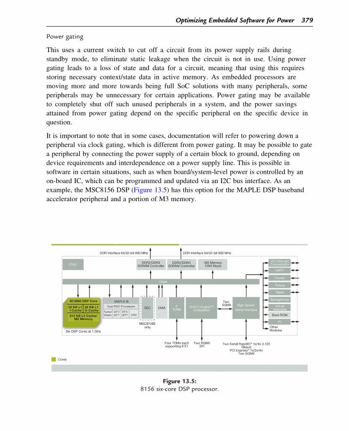
example, the MSC8156 DSP (Figure 13.5) has this option for the MAPLE DSP baseband
accelerator peripheral and a portion of M3 memory.
Figure 13.5:8156 six-core DSP processor.
Optimizing Embedded Software for Power 379

Clock gating
As the name implies, this shuts down clocks to a circuit or portion of a clock tree in a
device. As dynamic power is consumed during state change triggered by clock toggling (as
we discussed in the introductory portion of this chapter), clock gating enables the
programmer to cut dynamic power through the use of a single (or a few) instructions.
Clocking of a processor core like a DSP is generally separated into trees stemming from a
main clock PLL into various clock domains as required by design for core, memories, and
peripherals, and DSPs generally enable levels of clock gating in order to customize a
power-saving solution.
Example low-power modes
As an example, the Freescale MSC815x DSPs provide various levels of clock gating in the
core subsystem and peripheral areas. Gating clocks to a core may be done in the form of
STOP and WAIT instructions. STOP mode gates clocks to the DSP core and the entire core
subsystem (L1 and L2 caches, M2 memory, memory management, debug and profile unit)
aside from internal logic used for waking from the STOP state.
In order to safely enter STOP mode, as one may imagine, care must be taken to ensure
accesses to memory and cache are all complete, and no fetches/prefetches are under way.
The recommended process is:
Terminate any open L2 prefetch activity.
Stop all internal and external accesses to M2/L2 memory.
Close the subsystem slave port window (peripheral access path to M2 memory) by
writing to the core subsystem slave port general configuration register.
Verify slave port is closed by reading the register, and also testing access to the slave
port (at this point, any access to the core’s slave port will generate an interrupt).
Ensure STOP ACK bit is asserted in General Status Register to show subsystem is in
STOP state.
Enter STOP mode.
STOP state can be exited by initiating an interrupt. There are other ways to exit from STOP
state, including a reset or debug assertion from external signals.
The WAIT state gates clocks to the core and some of the core subsystem aside from the
interrupt controller, debug and profile unit, timer, and M2 memory, which enables faster
entering and exiting from WAIT state, but at the cost of greater power consumption. To
enter WAIT state, the programmer may simply use the WAIT instruction for a core. Exiting
WAIT, like STOP, may also be done via an interrupt.
380 Chapter 13
A particularly nice feature of these low-power states is that both STOP and WAIT mode
can be exited via either an enabled or a disabled interrupt. Wake-up via an enabled interrupt
follows the standard interrupt handling procedure: the core takes the interrupt, does a full
context switch, and then the program counter jumps to the interrupt service routine before
returning to the instruction following the segment of code that executed the WAIT (or
STOP) instruction. This requires a comparatively large cycle overhead, which is where
disabled interrupt waking becomes quite convenient. When using a disabled interrupt to exit
from either WAIT or STOP state, the interrupt signals the core using an interrupt priority
that is not “enabled” in terms of the core’s global interrupt priority level (IPL), and when
the core wakes it resumes execution where it left off without executing a context switch or
any ISR. An example using a disabled interrupt for waking the MSC8156 is provided at the
end of this section.
Clock gating to peripherals is also enabled, where the user may gate specific peripherals
individually as needed. This is available for the MSC8156’s serial interface, Ethernet
controller (QE), DSP accelerators (MAPLE), and DDR. As with STOP mode, when gating
clocks to any of these interfaces, the programmer must ensure that all accesses are
completed beforehand. Then, via the System Clock Control register, clocks to each of these
peripherals may be gated. In order to come out of the clock gated modes, a Power on Reset
is required, so this is not something that can be done and undone on the fly in a function,
but rather a setting that is decided at system configuration time.
Additionally, partial clock gating is possible on the high-speed serial interface components
(SERDES, OCN DMA, SRIO, RMU, PCI Express) and ddr so that they may be temporarily
put in a “doze state” in order to save power, but still maintain the functionality of providing
an acknowledge to accesses (in order to prevent internal or external bus lockup when
accessed by external logic).
Texas Instruments C6000 low-power modes
Another popular DSP family on the market is the C6000 series DSP from Texas Instruments
(TI). TI DSPs in the C6000 family provide a few levels of clock gating, depending on the
generation of C6000. For example, the previous generation C67x floating-point DSP has low-
power modes called “power-down modes”. These modes include PD1, PD2, PD3, and
“peripheral power down”, each of which gates clocking to various components in the silicon.
For example, PD1 mode gates clocks to the C67x CPU (processor core, data registers,
control registers, and everything else within the core aside from the interrupt controller).
The C67x can wake up from PD1 via an interrupt into the core. Entering power-down mode
PD1 (or PD2 / PD3) for the C67x is done via a register write (to CSR). The cost of entering
PD1 state is B9 clock cycles plus the cost of accessing the CSR register. As this
Optimizing Embedded Software for Power 381

power-down state only affects the core (and not cache memories), it is not comparable to
the Freescale’s STOP or WAIT state.
The two deeper levels of power down, PD2 and PD3, effectively gate clocks to the entire
device (all blocks which use an internal clock: internal peripherals, the CPU, cache, etc.).
The only way to wake up from PD2 and PD3 clock gating is via a reset, so PD2 and PD3
would not be very convenient or efficient to use mid-application.
Clock and voltage control
Some devices have the ability to scale voltage or clock, which may help optimize the power
scheme of a device/application. Voltage scaling, as the name implies, is the process of
lowering or raising the power. In the section on measuring current, VRMs were introduced
as one method. The main purpose of a VRM (voltage regulator module) is to control the
power/voltage supply to a device. Using a VRM, voltage scaling may be done through
monitoring and updating voltage ID (VID) parameters.
In general, as voltage is lowered, frequency/processor speed is sacrificed, so generally
voltage would be lowered when the demand from a DSP core or a certain peripheral is
reduced.
The TI C6000 devices provide a flavor of voltage scaling called SmartReflex®.
SmartReflex® enables automatic voltage scaling through a pin interface which provides
VID to a VRM. As the pin interface is internally managed, the software engineer does not
have much influence over this, so we will not cover any programming examples for this.
Clock control is available in many processors, which allows the changing of the values of
various PLLs in runtime. In some cases, updating the internal PLLs requires relocking the
PLLs, where some clocks in the system may be stopped, and this must be followed by a
soft reset (reset of the internal cores). Because of this inherent latency, clock scaling is not
very feasible during normal heavy operation, but may be considered if a processor’s
requirements over a long period of time are reduced (such as during times of low call
volume during the night for processors on a wireless base station).
When considering clock scaling, we must keep the following in mind: during normal
operation, running at a lower clock allows for lower dynamic power consumption, assuming
clock and power gating are never used. In practice, running a processor at a higher
frequency allows for more “free” cycles, which, as previously noted, can be used to hold
the device in a low-power/sleep mode � thus offsetting the benefits of such clock scaling.
Additionally, updating the clock for custom cases is time-intensive, and for some
processors, not an option at all � meaning clock frequency has to be decided at device
reset/power-on time, so the general rule of thumb is to enable enough clock cycles with
382 Chapter 13

some additional headroom for the real-time application being run, and to utilize other power
optimization techniques. Determining the amount of headroom varies from processor to
processor and application to application � at which point it makes sense to profile your
application in order to understand the number of cycles required for a packet/frame, and the
core utilization during this time period.
Once this is understood, measuring the power consumption for such a profile can be done,
as demonstrated earlier in this chapter in the profiling power section. Measure the average
power consumption at your main frequency options. (for example this could be 800 MHz
and 1 GHz), and then average in idle power over the headroom slots in order to get a head-
to-head comparison of the best-case power consumption.
Considerations and usage examples of low-power modes
Here we will summarize the main considerations for low-power mode usage, and then close
with a coding example demonstrating low-power mode usage in a real-time multimedia
application.
Consider available block functionality when in low-power mode:
• When in low-power modes, we have to remember that certain peripherals will not be
available to external peripherals, and peripheral buses may also be affected. As noted
earlier in this section, devices may take care of this, but this is not always the case. If
power gating a block, special care must be taken regarding shared external buses,
clocks, and pins.
• Additionally, memory states and validity of data must be considered. We will cover this
when discussing cache and DDR in the next section
Consider the overhead of entering and exiting low-power modes:
• When entering and exiting low -ower modes, in addition to overall power savings, the
programmer must ensure the cycle overhead of actually entering and exiting the low
power mode does not break real time constraints.
• Cycle overhead may also be affected by the potential difference in initiating a low
power mode by register access as opposed to by direct core instructions.
Low-power example
To demonstrate low power usage, we will refer to a Motion JPEG (MJPEG) application. In
this application, raw image frames are sent from a PC to an embedded DSP over Ethernet.
Each Ethernet packet contains 1 block of an image frame. A full raw QVGA image uses
B396 blocks plus a header. The DSP encodes the image in real time (adjustable from 1 to
301 frames per second), and sends the encoded Motion JPEG video back over Ethernet to
Optimizing Embedded Software for Power 383

be played on a demo GUI in the PC. The flow and a screenshot of this GUI are shown in
Figure 13.6.
The GUI will display not only the encoded JPEG image, but also the core utilization (as a
percentage of the maximum core cycles available).
For this application, we need to understand how many cycles encoding a frame of JPEG
consumes. Using this we can determine the maximum frame rate we can use and, in
parallel, also determine the maximum down time we have for low-power mode usage.
If we are close to the maximum core utilization for the real-time application, then using
low-power modes may not make sense (may break real-time constraints).
As noted in previous chapters, we could simply profile the application to see how many
cycles are actually spent per image frame, but this is already handled in the MJPEG
demo’s code using the core cycle counters in the OCE (on-chip emulator). The OCE is
a hardware block on the DSP that the profiler utilizes to get core cycle counts for use in
code profiling.
The MJPEG code in this case counts the number of cycles a core spends doing actual work
(handling an incoming Ethernet interrupt, dequeueing data, encoding a block of data into
JPEG format, enqueueing/sending data back over Ethernet).
The number of core cycles required to process a single block encode of data (and supporting
background data movement) is measured to be of the order of 13,000 cycles. For a full JPEG
image (B396 image blocks and Ethernet packets), this is approximately 5 million cycles.
Embedded computer board (8156 DSP)
Row
image fram
es
JPE
G fram
es
PC
Figure 13.6:DSP operating system Motion JPEG application.
384 Chapter 13
So 1 JPEG frame a second would work out to be 0.5% of a core’s potential processing
power, assuming a 1 GHz core that is handling all Ethernet I/O, interrupt context
switches, etc.
CyclesBlock Mgmt Encode5 13; 000
CyclesJPEG Frame5CyclesBlock Mgmt Encode3 3965 5; 148; 000
Core Utilization30FPSð%Þ5 301003OCECount
1; 000; 000; 0005 15:4%
In this example the DSP has up to six cores, and only one core would have to manage
Ethernet I/O; in a full multicore system, utilization per core drops to a range of 3 to
7%. A master core acts as the manager of the system, managing both Ethernet I/O,
intercore communication, and JPEG encoding, while the other slave cores are
programmed to solely focus on encoding JPEG frames. Because of this intercore
communication and management, the drop in cycle consumption from one core to four
or six is not linear.
Based on cycle counts from the OCE, we can run a single core, which is put in a sleep
state for 85% of the time, or a multicore system which uses sleep state up to 95% of
the time.
This application also uses only a portion of the SoC peripherals (Ethernet, JTAG, a single
DDR, and M3 memory). So we can save power by gating the full HSSI System (Serial
Rapid IO, PCI Express), the MAPLE accelerator, and the second DDR controller.
Additionally, for our GUI demo, we are only showing four cores, so we can gate cores 4
and 5 without affecting this demo as well.
Based on the above, and what we have discussed in this section, here is the plan we want to
follow:
• At application start up:
Clock gate the unused MAPLE accelerator block (MAPLE described later in this
chapter).
NOTES:
MAPLE power pins share a power supply with core voltage. If the power supply to
MAPLE was not shared, we could completely gate power. Due to shared pins on
the development board, the most effective choice we have is to gate the MAPLE
clock.
MAPLE automatically goes into a doze state, which gates part of the clocks to the
block when it is not in use. Because of this, power savings from entirely gating
MAPLE may not be massive.
Clock gate the unused HSSI (high-speed serial interface).
Optimizing Embedded Software for Power 385

NOTES:
We could also put MAPLE into a doze state, but this gates only part of the clocks.
Since we will not be using any portion of these peripherals, complete clock gating
is more power efficient.
Clock gate the unused second DDR controller.
NOTES:
When using VTB, the OS places buffer space for VTB in the second DDR memory,
so we need to be sure that this is not needed.
• During application runtime:
At runtime, QE (Ethernet Controller), DDR, interconnect, and cores 1�4 will be
active. Things we must consider for these components include:
The Ethernet Controller cannot be shut down or put into a low power state � as
this is the block that receives new packets (JPEG blocks) to encode. Interrupts from
the Ethernet controller can be used to wake our master core from low-power mode.
Active core low-power modes:
WAIT mode enables core power savings, while allowing the core to be
woken up in just a few cycles by using a disabled interrupt to signal exit from
WAIT.
STOP mode enables greater core savings by shutting down more of the
subsystem than WAIT (including M2), but requires slightly more time to wake
due to more hardware being re-enabled. If data is coming in at high rates,
and the wake time is too long, we could get an overflow condition, where
packets are lost. This is unlikely here due to the required data rate of the
application.
The first DDR contains sections of program code and data, including parts of the
Ethernet handling code. (This can be quickly checked and verified by looking at the
program’s .map file.) Because the Ethernet controller will be waking the master
core from WAIT state, and the first thing the core will need to do out of this state
is to run the Ethernet handler, we will not put DDR0 to sleep.
We can use the main background routine for the application to apply these changes without
interfering with the RTOS. This code segment is shown in Figure 13.7 with power-down-
related code.
Note that the clock gating must be done by only one core as these registers are system level
and access is shared by all cores.
This code example demonstrates how a programmer using the OS can make use of the
interrupt APIs in order to recover from STOP or wait state without actually requiring a
context switch. In the MJPEG player, as noted above, raw image blocks are received via
Ethernet (with interrupts), and then shared via shared queues (with interrupts). The master
386 Chapter 13

static void appBackground(void)
{
os_hwi_handle hwi_num;
if (osGetCoreID() == 0)
{
*((unsigned int*)0xfff28014) = 0xF3FCFFFB;//HSSI CR1
*((unsigned int*)0xfff28018) = 0x0000001F;//HSSI CR2
*((unsigned int*)0xfff28034) = 0x20000E0E; //GCR5
*((unsigned int*)0xfff24000) = 0x00001500; //SCCR
}
osMessageQueueHwiGet(CORE0_TO_OTHERS_MESSAGE, &hwi_num);
while(1)
{
osHwiSwiftDisable();
osHwiEnable(OS_HWI_PRIORITY10);
stop();//wait();
osHwiEnable(OS_HWI_PRIORITY4);
osHwiSwiftEnable();
osHwiPendingClear(hwi_num);
MessageHandler(CORE0_TO_OTHERS_MESSAGE);
}
}
Figure 13.7:Code segment with power-down-related code.
Optimizing Embedded Software for Power 387
core will have to use context switching to read new Ethernet frames here, but slave cores
only need to wake up and go to the MessageHandler function.
We take advantage of this fact by enabling only higher-priority interrupts before going to
sleep:
osHwiSwiftDisable();
osHwiEnable(OS_HWI_PRIORITY10);
Then when a slave core is asleep, if a new queue message arrives on an interrupt, the core
will be woken up (on context switch), and standard interrupt priority levels will be restored.
The core will then go and manage the new message without context switch overhead by
calling the MessageHandler() function. In order to verify our power savings, we will take a
baseline power reading before optimizing across the relevant power supplies, and then
measure the incremental power savings of each step.
The processor board has power for cores, accelerators, HSSI, and M3 memory connected to
the same power supply, simplifying data collection. Since these supplies and DDR are the
only blocks we are optimizing, we shall measure improvement based on these supplies alone.
Figure 13.8 provides a visual on the relative power consumed by the relevant power
supplies (1V: core, M3, HSSI, MAPLE accelerators, and DDR) across the power-down
steps used above. Note that actual power numbers are not provided to avoid any potential
non-disclosure issues.
The first two bars provide reference points � indicating the power consumption for these
supplies using a standard FIR filter in a loop and the power consumption when the cores
are held in debug state (not performing any instructions, but not in a low-power mode).
With our steps we can see that there was nearly a 50% reduction in power consumption
across the relevant supplies for the Motion JPEG demo with the steps laid out above, with
each step providing B5% reduction in power, with the exception of the STOP and WAIT
power modes, which are closer to 15�20% savings.
One thing to keep in mind is that, while the MJPEG demo is the perfect example to
demonstrate low-power modes, it is not highly core-intensive, so as we progress through
different optimization techniques, we will be using other examples as appropriate.
Optimizing data flow
Reducing power consumption for memory accesses
Because clocks have to be activated not only in the core components, but also in buses, and
memory cells, memory-related functionality can be quite power-hungry, but luckily memory
388 Chapter 13

access and data paths can also be optimized to reduce power. This section will cover
methods to optimize power consumption with regard to memory accesses to DDR and
SRAM memories by utilizing knowledge of the hardware design of these memory types.
Then we will cover ways to take advantage of other specific memory set-ups at the SoC
level. Common practice is to optimize memory in order to maximize the locality of critical
or heavily used data and code by placing as much in cache as possible. Cache misses incur
not only core stall penalties, but also power penalties as more bus activity is needed, and
higher-level memories (internal device SRAM, or external device DDR) are activated and
consume power. As a rule, access to higher-level memory such as DDR is not as common
as internal memory accesses, so high-level memory accesses are easier to plan, and thus
optimize.
DDR overview
The highest level of memory we will discuss here is external DDR memory. To optimize
DDR accesses in software, first we need to understand the hardware that the memory
consists of. DDR SDRAM, as the DDR (dual data rate) name implies, takes advantage of
Total Consumption Power Savings per Step
Standard FIRLoop
Device inDebug State(not running)
BaselineMJPEG (noPD modes)
Clock GateMAPLE
Clock GateHSSI
Gate HSSI Gate 2ndDDR
Using WAITMode for PD
Using STOPMode for PD
Figure 13.8:Power consumption savings in PD modes.
Optimizing Embedded Software for Power 389
both edges of the DDR clock source in order to send data, thus doubling the effective data
rate at which data reads and writes may occur. DDR provides a number of different types
of features which may affect total power utilization, such as EDC (error detection), ECC
(error correction), different types of bursting, programmable data refresh rates,
programmable memory configuration allowing physical bank interleaving, page
management across multiple chip selects, and DDR-specific sleep modes.
• Key DDR vocabulary to be discussed
• Chip Select (also known as Physical Bank): selects a set of memory chips
(specified as a “rank”) connected to the memory controller for accesses.
• Rank: specifies a set of chips on a DIMM to be accessed at once. A Double Rank
DIMM, for example, would have two sets of chips � differentiated by chip select.
When accessed together, each rank allows for a data access width of 64 bits (or 72
with ECC).
• Rows are address bits enabling access to a set of data, known as a “page” � so row
and page may be used interchangeably.
• Logical banks, like row bits, enable access to a certain segment of memory. By
standard practice, the row bits are the MSB address bits of DDR, followed by the
bits to select a logical bank, finally followed by column bits.
• Column bits are the bits used to select and access a specific address for reading or
writing.
On a typical embedded processor, like a DSP, the DSPs’ DDR SDRAM controller is
connected to either discrete memory chips or a DIMM (dual inline memory module), which
contains multiple memory components (chips). Each discrete component/chip contains
multiple logical banks, rows, and columns which provide access for reads and writes to
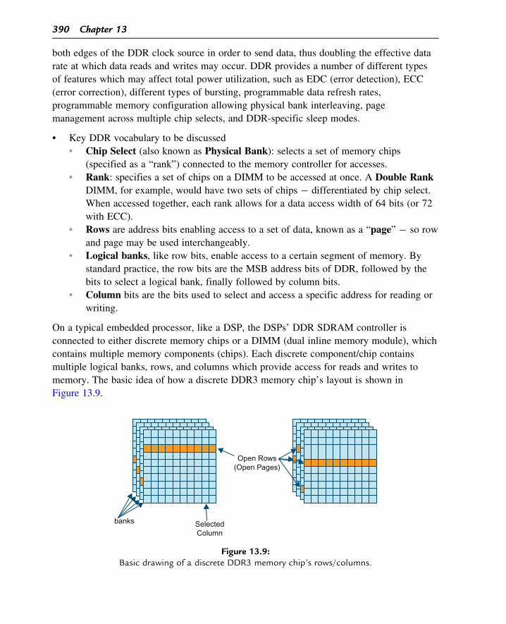
memory. The basic idea of how a discrete DDR3 memory chip’s layout is shown in
Figure 13.9.
banks SelectedColumn
Open Rows(Open Pages)
Figure 13.9:Basic drawing of a discrete DDR3 memory chip’s rows/columns.
390 Chapter 13
Standard DDR3 discrete chips are commonly made up of eight logical banks, which
provide addressability as shown above. These banks are essentially tables of rows and
columns. The action to select a row effectively opens that row (page) for the logical bank
being addressed. So different rows can be simultaneously open in different logical banks, as
illustrated by the active or open rows highlighted in the picture. A column selection gives
access to a portion of the row in the appropriate bank.
When considering sets of memory chips, the concept of chip select is added to the equation.
Using chip selects, also known as “physical banks”, enables the controller to access a
certain set of memory modules (up to 1 GB for the MSC8156, 2 GB for MSC8157 DSPs
from Freescale for example) at a time. Once a chip select is enabled, access to the selected
memory modules with that chip select are activated, using page selection (rows), banks, and
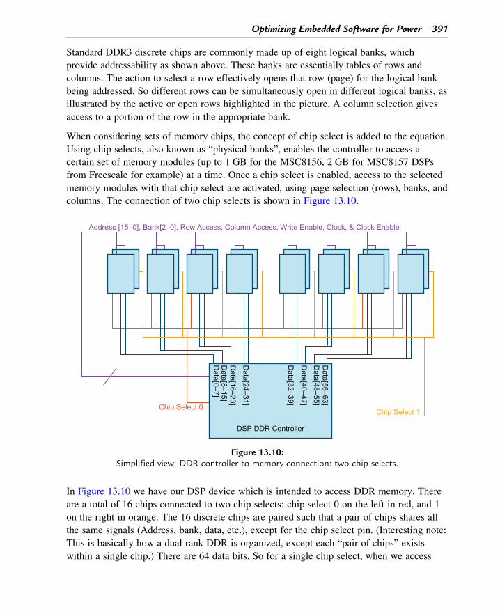
columns. The connection of two chip selects is shown in Figure 13.10.
In Figure 13.10 we have our DSP device which is intended to access DDR memory. There
are a total of 16 chips connected to two chip selects: chip select 0 on the left in red, and 1
on the right in orange. The 16 discrete chips are paired such that a pair of chips shares all
the same signals (Address, bank, data, etc.), except for the chip select pin. (Interesting note:
This is basically how a dual rank DDR is organized, except each “pair of chips” exists
within a single chip.) There are 64 data bits. So for a single chip select, when we access
Address [15–0], Bank[2–0], Row Access, Column Access, Write Enable, Clock, & Clock Enable
DSP DDR Controller
Data[56–63]
Data[48–55]
Data[40–47]
Data[32–39]
Data[24–31]
Data[16–23]
Data[8–15]
Data[0–7]
Chip Select 0Chip Select 1
Figure 13.10:Simplified view: DDR controller to memory connection: two chip selects.
Optimizing Embedded Software for Power 391

DDR and write 64 contiguous bits of data to DDR memory space in our application, the
DDR controller does the following:
• Selecting chip select based on your address (0 for example).
• Opening the same page (row) for each bank on all eight chips using the DDR address
bits during the Row Access phase.
• New rows are opened via the ACTIVE command, which copies data from the row to a
“row buffer” for fast access.
• Rows that were already opened do not require an active command and can skip this
step.
• During the next phase, the DDR controller will select the same column on all eight
chips. This is the column-access phase.
• Finally, the DDR controller will write the 64 bytes to the now open row buffers for
each of the eight separate DDR chips which each input eight bits.
As there is a command to open rows, there is also one to close rows, called PRECHARGE,
which tells the DDR modules to store the data from the row buffers back to the actual DDR
memory in the chip, thus freeing up the row buffer. So when switching from one row to the
next in a single DDR bank, we have to PRECHARGE the open row to close it, and then
ACTIVATE the row we wish to start accessing.
A side effect of an ACTIVATE command is that the memory is automatically read and
written � thus REFRESHing it. If a row in DDR is PRECHARGED, then it must be
periodically refreshed (read/re-written with the same data) to keep data valid. DDR
controllers have an autorefresh mechanism that does this for the programmer.
DDR data flow optimization for power
Now that the basics of DDR accesses have been covered, we can cover how DDR accesses
can be optimized for minimal power consumption. As is often the case, optimizing for
minimal power consumption is beneficial for performance as well.
DDR consumes power in all states, even when the CKE (clock enable � enabling the DDR
to perform any operations) is disabled, though this is minimal. One technique to minimize
DDR power consumption is made available by some DDR controllers which have a power
saving mode that de-asserts the CKE pin � greatly reducing power. In some cases, this is
called Dynamic Power Management Mode, which can be enabled via the
DDR_SDRAM_CFG[DYN_PWR] register. This feature will de-assert CKE when no
memory refreshes or accesses are scheduled. If the DDR memory has self-refresh
capabilities, then this power-saving mode can be prolonged as refreshes are not required
from the DDR controller.
392 Chapter 13

This power-saving mode does impact performance to some extent, as enabling CKE when a
new access is scheduled adds a latency delay.
Tools such as Micron’s DDR power calculator can be used to estimate power consumption
for DDR. If we choose 1 GB x8 DDR chips with 2125 speed grade, we can see estimates
for the main power-consuming actions on DDR. Power consumption for non-idle operations
is additive, so total power is the idle power plus non-idle operations.
Idle with no rows open and CKE low is shown as: 4.3 mW (IDD2p)
Idle with no rows open and CKE high is shown as: 24.6 mW (IDD2n)
Idle with rows open and no CKE low is shown as: 9.9 mW (IDD3p)
Idle with rows open and CKE high is shown as: 57.3 mW (IDD3n)
ACTIVATE and PRECHARGE is shown as consuming 231.9 mW
REFRESH is shown as 3.9 mW
WRITE is shown as 46.8 mW
READ is shown as 70.9 mW
We can see that using the Dynamic Power Management mode saves up to 32 mW of
power, which is quite substantial in the context of DDR usage.
Also, it is clear that the software engineer must do whatever possible to minimize
contributions to power from the main power contributors: ACTIVATE, PRECHARGE,
READ, and WRITE operations.
The power consumption from row activation/precharge is expected as DDR needs to
consume a considerable amount of power in decoding the actual ACTIVATE instruction
and address followed by transferring data from the memory array into the row buffer.
Likewise, the PRECHARGE command also consumes a significant amount of power in
writing data back to the memory array from row buffers.
Optimizing power by timing
One can minimize the maximum “average power” consumed by ACTIVATE commands
over time by altering the timing between row activate commands, tRC (a setting the
programmer can set at start up for the DDR controller). By extending the time required
between DDR row activates, the maximum power spike of activates is spread, so the
amount of power pulled by the DDR in a given period of time is lessened, though the total
power for a certain number of accesses will remain the same. The important thing to note
here is that this can help with limiting the maximum (worst-case) power seen by the
device, which can be helpful when having to work within the confines of a certain
hardware limitation (power supply, limited decoupling capacitance to DDR supplies on the
board, etc.).
Optimizing Embedded Software for Power 393

Optimizing with interleaving
Now that we understand that our main enemy in power consumption on DDR is the
activate/precharge commands (for both power and performance), we can devise plans to
minimize the need for such commands. There are a number of things to look at here, the
first being address interleaving, which will reduce ACTIVATE/PRECHARGE command
pairs via interleaving chip selects (physical banks) and additionally by interleaving logical
banks.
In setting up the address space for the DDR controller, the row bits and chip select/bank
select bits may be swapped to enable DDR interleaving, whereby changing the higher-order
address enables the DDR controller to stay on the same page while changing chip selects
(physical banks) and then changing logical banks before changing rows. The software
programmer can enable this by register configuration in most cases.
Optimizing memory software data organization
We also need to consider the layout of our memory structures within DDR. If using large
ping-pong buffers, for example, the buffers may be organized so that each buffer is in its
own logical bank. This way, if DDR is not interleaved, we still can avoid unnecessary
ACTIVATE/PRECHARGE pairs if a pair of buffers is larger than a single row (page).
Optimizing general DDR configuration
There are other features available to the programmer which can positively or negatively
affect power, including “open/closed” page mode. Closed page mode is a feature available
in some controllers which will perform an auto-precharge on a row after each read or write
access. This of course unnecessarily increases the power consumption in DDR as a
programmer may need to access the same row 10 times, for example; closed page mode
would yield at least 9 unneeded PRECHARGE/ACTIVATE command pairs. In the example
DDR layout discussed above, this could consume an extra 231.9 mW � 95 2087.1 mW.
As you may expect, this has an equally negative effect on performance due to the stall
incurred during memory PRECHARGE and ACTIVATE.
Optimizing DDR burst accesses
DDR technology has become more restrictive with each generation: DDR2 allows 4-beat
bursts and 8-beat bursts, whereas DDR3 only allows 8. This means that DDR3 will treat all
burst lengths as 8-beat (bursts of 8 accesses long). So for the 8-byte (64 bit) wide DDR
394 Chapter 13

accesses we have been discussing here, accesses are expected to be 8 beats of 8 bytes, or 64
bytes long.
If accesses are not 64 bytes wide, there will be stalls due to the hardware design. This
means that if the DDR memory is accessed only for reading (or writing) 32 bytes of data at
a time, DDR will only be running at 50% efficiency, as the hardware will still perform
reads/writes for the full 8-beat burst, though only 32 bytes will be used. Because DDR3
operates this way, the same amount of power is consumed whether doing 32-byte or 64-
byte-long bursts to our memory here. So for the same amount of data, if doing 4-beat (32
byte) bursts, the DDR3 would consume approximately twice the power.
The recommendation here then is to make all accesses to DDR full 8-beat bursts in order to
maximize power efficiency. To do this, the programmer must be sure to pack data in the
DDR so that accesses to the DDR are in at least 64-byte-wide chunks. Packing data so it is
64-byte-aligned or any other alignment can be done through the use of pragmas.
The concept of data packing can be used to reduce the amount of used memory as well. For
example, packing eight single bit variables into a single character reduces memory footprint
and increases the amount of usable data the core or cache can read in with a single burst.
In addition to data packing, accesses need to be 8-byte-aligned (or aligned to the burst
length). If an access is not aligned to the burst length, for example, let’s assume an 8-byte
access starts with a 4-byte offset, both the first and second access will effectively become
4-beat bursts, reducing bandwidth utilization to 50% (instead of aligning to the 64-byte
boundary and reading data in with one single burst).
SRAM and cache data flow optimization for power
Another optimization related to the usage of off-chip DDR is avoidance: avoiding using
external off-chip memory and maximizing accesses to internal on-chip memory saves the
additive power draw that occurs when activating not only internal device buses and clocks,
but also off-chip buses, memory arrays, etc.
High-speed memory close to the DSP processor core is typically SRAM memory, whether
it functions in the form of cache or as a local on-chip memory. SRAM differs from
SDRAM in a number of ways (such as no ACTIVATE/PRECHARGE, and no concept of
REFRESH), but some of the principles of saving power still apply, such as pipelining
accesses to memory via data packing and memory alignment.
The general rule for SRAM access optimization is that accesses should be optimized for
higher performance. The fewer clock cycles the device spends doing a memory operation,
the less time that memory, buses, and core are all activated for said memory operation.
Optimizing Embedded Software for Power 395
SRAM (all memory) and code size
As programmers, we can affect this in both program and data organization. Programs may
be optimized for minimal code size (by a compiler, or by hand), in order to consume a
minimal amount of space. Smaller programs require less memory to be activated to read the
program. This applies not only to SRAM, but also to DDR and any type of memory � less
memory having to be accessed implies a lesser amount of power drawn.
Aside from optimizing code using the compiler tools, other techniques such as instruction
packing, which are available in some embedded core architectures, enable fitting maximum
code into a minimum set of space. The VLES (variable-length execution set) instruction
architecture allows the program to pack multiple instructions of varying sizes into a single
execution set. As execution sets are not required to be 128-bit-aligned, instructions can be
packed tightly, and the prefetch, fetch, and instruction dispatch hardware will handle
reading the instructions and identifying the start and end of each instruction set.
Additionally, size can be saved in code by creating functions for common tasks. If tasks are
similar, consider using the same function with parameters passed to determine the variation
to run instead of duplicating the code in software multiple times.
Be sure to make use of combined functions where available in the hardware. For example,
in the Freescale StarCore architecture, using a multiply accumulate (MAC) instruction,
which takes one pipelined cycle, saves space and performance in addition to power
compared with using separate multiple and add instructions.
Some hardware provides code compression at compile time and decompression on the fly,
so this may be an option depending on the hardware the user is dealing with. The problem
with this strategy is related to the size of compression blocks. If data is compressed into
small blocks, then not as much compression optimization is possible, but this is still more
desirable than the alternative. During decompression, if code contains many branches or
jumps, the processor will end up wasting bandwidth, cycles, and power decompressing
larger blocks that are hardly used.
The problem with the general strategy of minimizing code size is the inherent conflict
between optimizing for performance and space. Optimizing for performance generally
does not always yield the smallest program, so determining ideal code size vs. cycle
performance in order to minimize power consumption requires some balancing and
profiling. The general advice here is to use what tricks are available to minimize code
size without hurting the performance of a program that meets real-time requirements.
The 80/20 rule of applying performance optimization to the 20% of code that performs
80% of the work, while optimizing the remaining 80% of code for size, is a good
practice to follow.
396 Chapter 13

SRAM power consumption and parallelization
It is also advisable to optimize data accesses in order to reduce the cycles in which SRAM
is activated, pipelining accesses to memory, and organizing data so that it may be accessed
consecutively. In systems like the MSC8156, the core/L1 caches connect to the M2 memory
via a 128-bit wide bus. If data is organized properly, this means that 128-bit data accesses
from M2 SRAM could be performed in one clock cycle each, which would obviously be
beneficial when compared to doing 16 independent 8-bit accesses to M2 in terms of
performance and power consumption.
An example showing how one may use move instructions to write 128 bits of data back to
memory in a single instruction set (VLES) is provided below:
[
MOVERH.4F d0:d1:d2:d3,(r4)1 n0
MOVERL.4F d4:d5:d6:d7,(r5)1 n0
]
We can parallelize memory accesses in a single instruction (as with the above where both
of the moves are performed in parallel) and, even if the accesses are to separate memories
or memory banks, the single-cycle access still consumes less power than doing two
independent instructions in two cycles.
Another note: as with DDR, SRAM accesses need to be aligned to the bus width in order to
make full use of the bus.
Data transitions and power consumption
SRAM power consumption may also be affected by the type of data used in an application.
Power consumption is affected by the number of data transitions (from 0 s to 1 s) in
memory as well. This power effect also trickles down to the DSP core processing elements,
as found by Kojima et al. Processing mathematical instructions using constants consumes
less power at the core than with dynamic variables. In many devices, because pre-charging
memory to reference voltage is common practice in SRAM memories, power consumption
is also proportional to the number of zeros as the memory is pre-charged to a high state.
Using this knowledge, it goes without saying that re-use of constants where possible and
avoiding zeroing out memory unnecessarily will, in general, save the programmer some power.
Cache utilization and SoC memory layout
Cache usage can be thought of in the opposite manner to DDR usage when designing a
program. An interesting detail about cache is that both dynamic and static power increase
Optimizing Embedded Software for Power 397

with increasing cache sizes; however, the increase in dynamic power is small. The increase
in static power is significant, and becomes increasingly relevant for smaller feature sizes.
As software programmers, we have no impact on the actual cache size available on a
device, but when it is provided, based on the above, it is our duty to use as much of it as
possible!
For SoC-level memory configuration and layout, optimizing the most heavily used routines
and placing them in the closest cache to the core processors will offer not only the best
performance, but also better power consumption.
Explanation of locality
The reason the above is true is thanks to the way caches work. There are a number of
different cache architectures, but they all take advantage of the principle of locality. The
principle of locality basically states that if one memory address is accessed, the probability
of an address nearby being accessed soon is relatively high. Based on this, when a cache
miss occurs (when the core tries to access memory that has not been brought into the
cache), the cache will read the requested data in from higher-level memory one line at a
time. This means that if the core tries to read a 1-byte character from cache, and the data is
not in the cache, then there is a miss at this address. When the cache goes to higher-level
memory (whether it be on-chip memory or external DDR, etc.), it will not read in an 8-bit
character, but rather a full cache line. If our cache uses cache sizes of 256 bytes, then a
miss will read in our 1-byte character, along with 255 more bytes that happen to be on the
same line in memory.
This is very effective in reducing power if used in the right way. If we are reading an array
of characters aligned to the cache line size, once we get a miss on the first element,
although we pay a penalty in power and performance for cache to read in the first line of
data, the remaining 255 bytes of this array will be in cache. When handling image or video
samples, a single frame would typically be stored this way, in a large array of data. When
performing compression or decompression on the frame, the entire frame will be accessed
in a short period of time, thus it is spatially and temporally local.
Again, let’s use the example of the six-core MSC8156 DSP SoC. In this SoC, there are two
levels of cache for each of the six DSP processor cores: L1 cache (which consists of 32 KB
of instruction and 32 KB of data cache), and a 512 KB L2 memory which can be
configured as L2 cache or M2 memory. At the SoC level, there is a 1 MB memory shared
by all cores called M3. L1 cache runs at the core processor speed (1 GHz), L2 cache
effectively manages data at the same speed (double the bus width, half the frequency), and
M3 runs at up to 400 MHz. The easiest way to make use of the memory hierarchy is to
enable L2 as cache and make use of data locality. As discussed above, this works when
398 Chapter 13
data is stored with high locality. Another option is to DMA data into L2 memory
(configured in non-cache mode). We will discuss DMA in a later section.
When we have a large chunk of data stored in M3 or in DDR, the MSC8156 can draw this
data in through the caches simultaneously. L1 and L2 caches are linked, so a miss from L1
will pull 256 bytes of data in from L2, and a miss from L2 will pull data in at 64 bytes at a
time (64 B line size) from the requested higher-level memory (M3 or DDR). Using L2
cache has two advantages over going directly to M3 or DDR. First, it is running at
effectively the same speed as L1 (though there is a slight stall latency here, it is negligible),
and second, in addition to being local and fast, it can be up to 16 times larger than L1
cache, allowing us to keep much more data in local memory than just L1 alone would.
Explanation of set-associativity
All caches in the MSC8156 are eight-way set-associative. This means that the caches are
split into eight different sections (“ways”). Each section is used to access higher-level
memory, meaning that a single address in M3 could be stored in one of eight different
sections (ways) of L2 cache, for example. The easiest way to think of this is that the section
(way) of cache can be overlaid onto the higher-level memory x times. So so if L2 is set up
as all cache, the following equation calculates how many times each set of L2 memory is
overlaid onto M3:
# of overlays O5M3size
ðL2size=8waysÞ
51MB
ð512KB=8Þ 5 16384 overlays
In the MSC8156, a single way of L2 cache is 64 KB in size, so addresses are from
03 0000_0000 to 03 0001_0000 hexadecimal. If we consider each way of cache
individually, we can explain how a single way of L2 is mapped to M3 memory. M3
addresses start at 0xC000_0000. So M3 addresses 0xC000_0000, 0xC001_0000,
0xC002_0000, 0xC003_0000, 0xC004_0000, etc. (up to 16 K times) all map to the same
line of a way of cache. So if way #1 of L2 cache has valid data for M3’s 0xC000_0000,
and the core processor wants to next access 0xC001_0000, what is going to happen?
If the cache has only one way set-associativity, then the line of cache containing
0xC000_0000 will have to be flushed back to cache and re-used in order to cache
0xC001_0000. In an eight-way set-associative cache, however, we can take advantage of
the other 73 64 KB sections (ways) of cache. So we can potentially have 0xC000_0000
stored in way #1, and the other seven ways of cache have their first line of cache as empty.
In this case, we can store our new memory access to 0xC001_0000 in way #2.
Optimizing Embedded Software for Power 399

So, what happens when there is an access to 0xC000_0040? (03 40 5 5 64 B). The
answer here is that we have to look at the second cache line in each way of L2 to see if it is
empty, as we were only considering the first line of cache in our example above. So here
we now have eight more potential places to store a line of data (or program).
Figure 13.11 shows a four-way set-associative cache connecting to M3. In this figure, we
can see that every line of M3 maps to four possible lines of the cache (one for each way).
So line 0xC000_0040 maps to the second line (second “set”) of each way in the cache. So
when the core wants to read 0xC000_0040, but the first way has 0xC000_0100 in it, the
cache can load the core’s request into any of the other three ways if their second lines are
empty (invalid).
The reason for discussing set-associativity of caches is that it does have some effect on
power consumption (as one might imagine). The goal for optimizing power consumption
(and performance) when using cache is to maximize the hit rate in order to minimize
accesses to external buses and hardware caused by misses. Set-associativity is normally
already determined by hardware, but, if the programmer can change set associativity,
Figure 13.11:Set-associativity by cache line: four-way set-associative cache.
400 Chapter 13

set-associative caches maintain a higher hit-rate than directly mapped caches, and thus draw
lower power.
Memory layout for cache
While having an eight-way set-associative architecture is statistically beneficial in
improving hit ratio and power consumption, the software programmer may also directly
improve hit ratio in the cache, and thus lower power by avoiding conflicts in cache.
Conflicts in cache occur when the core needs data that will replace cache lines with
currently valid data that will be needed again.
We can organize memory in order to avoid these conflicts in a few different ways. For
memory segments we need simultaneously, it is important to pay attention to the size of
ways in the cache. In our eight-way L2 cache, each way is 64 KB. As we discussed before,
we can simultaneously load eight cache lines with the same lower 16 bits of address
(03 0000_xxxx).
Another example is if we are working with nine arrays with 64 KB of data simultaneously.
If we organize each array contiguously data will be constantly thrashed as all arrays share
the same 64 KB offset. If the same indices of each array are being accessed simultaneously,
we can offset the start of some of the arrays by inserting buffer, so that each array does not
map to the same offset (set) within a cache way.
When data sizes are larger than a single way, the next step is to consider reducing the
amount of data that is pulled into the cache at a time � process smaller chunks at a time.
Write-back vs. write-through caches
Some caches are designed as either “write-back” or “write-through” caches, and others,
such as the MSC815x series DSPs, are configurable as either. Write-back and write-
through buffering differs in how data from the core is managed by the cache in the case
of writes.
Write-back is a cache writing scheme in which data is written only to the cache. The main
memory is updated when the data in the cache is replaced. In the write-through cache write
scheme, data is written simultaneously to the cache and to memory. When setting up cache
in software, we have to weigh the benefits of each of these. In a multicore system,
coherency is of some concern, but so are performance and power. Coherency refers to how
up-to-date data in main memory is compared to the caches. The greatest level of multicore
coherency between internal core caches and system level memory is attained by using
write-through caching, as every write to cache will immediately be written back to system
Optimizing Embedded Software for Power 401

memory, keeping it up to date. There are a number of down sides to write-through caching
including:
• core stalls during writes to higher-level memory;
• increased bus traffic on the system buses (higher chance of contention and system-level
stalls);
• increased power consumption as the higher-level memories and buses are activated for
every single memory write.
The write-back cache scheme, on the other hand, will avoid all of the above disadvantages
at the cost of system-level coherency. For optimal power consumption, a common approach
is to use the cache in write-back mode, and strategically flush cache lines/segments when
the system needs to be updated with new data.
Cache coherency functions
In addition to write-back and write-through schemes, specific cache commands should also
be considered. Commands include:
• invalidation sweep: invalidating a line of data by clearing valid and dirty bits
(effectively just re-labeling a line of cache as “empty”);
• synchronization sweep: writing any new data back to cache and removing the dirty
label;
• flush sweep: writing any new data back to cache and invalidating the line;
• fetch: fetch data into the cache.
Generally these operations can be performed by either cache line, a segment of the cache,
or as a global operation. When it is possible to predict that a large chunk of data will be
needed in the cache in the near future, performing cache sweep functions on larger
segments will make better use of the full bus bandwidths and lead to fewer stalls by the
core. As memory accesses all require some initial memory access set-up time, but after set-
up bursts will flow at full bandwidth, making use of large prefetches will save power when
compared to reading in the same amount of data line by line so long as this is done
strategically so as to avoid the data we want from being thrashed before the core actually
gets to use it.
When using any of these instructions, we have to be careful about the effect it has on
the rest of the cache. For instance, performing a fetch from higher-level memory into
cache may require replacing contents currently in the cache. This could result in
thrashing data in the cache and invalidating cache in order to make space for the data
being fetched.
402 Chapter 13

Compiler cache optimizations
In order to assist with the above, compilers may be used to optimize cache power
consumption by reorganizing memory or memory accesses for us. Two main techniques
available are array merging and loop interchanging, explained below.
Array merging organizes memory so that arrays accessed simultaneously will be at
different offsets (different “sets”) from the start of a way. Consider the following two array
declarations below:
int array1[ array_size ];
int array2[ array_size ];
The compiler can merge these two arrays as shown below:
struct merged_arrays
{
int array1;
int array2;
} new_array[ array_ size ]
In order to re-order the way that high-level memory is read into cache, reading in smaller
chunks to reduce the chance of thrashing loop interchanging can be used. Consider the code
below:
for (i50; i,100; i5i11)
for (j50; j,200; j5j11)
for (k50; k,10000; k5k11)
z[ k ][ j ] 5 10 * z[ k ][ j ];
By interchanging the second and third nested loops, the compiler can produce the
following code, decreasing the likelihood of unnecessary thrashing during the innermost
loop.
for (i50; i,100; i5i11)
for (k50; k,10000; k5k11)
for (j50; j,200; j5j11)
z[ k ][ j ] 5 10 * z[ k ][ j ];
Peripheral/communication utilization
When considering reading and writing of data, of course, we cannot just think about
memory access: we need to pull data into and out of the device as well. As such, for the
Optimizing Embedded Software for Power 403

final portion of data path optimization we will look at how to minimize power consumption
in commonly used embedded processor (I/O) peripherals.
Things to consider include the peripheral’s burst size, speed grade, transfer width, and
general communication modes. The main standard forms of peripheral communication for
embedded processors include DMA (direct memory access), SRIO (serial rapid I/O),
Ethernet, PCI Express, and RF antenna interfaces. I2C and UART are also commonly used,
though mostly for initialization and debug purposes.
The fact that communication interfaces usually require their own PLLs/clocks increases the
individual power consumption impact. The higher-clocked peripherals that we need to
consider as the main power consumers are the DMA, SRIO, Ethernet, and PCI Express.
Clock gating and peripheral low-power modes for these peripherals were discussed in the
low-power modes section of this chapter, so this section will talk about how to optimize
actual usage.
Although each protocol is different for the I/O peripherals and the internal DMA, they all
share the fact that they are used to read/write data. As such, one basic goal is to
maximize the throughput while the peripheral is active in order to maximize efficiency
and the time the peripheral/device can be in a low-power state, thus minimizing the active
clock times.
The most basic way to do this is to increase transfer/burst size. For DMA, the programmer
has control over burst size and transfer size in addition to the start/end address (and can
follow the alignment and memory accessing rules we discussed in earlier subsections of
data path optimization). Using the DMA, the programmer can decide not only the
alignment, but also the transfer “shape”, for lack of a better word. What this means is that
using the DMA, the programmer can transfer blocks in the form of two-dimensional, three-
dimensional, and four-dimensional data chunks, thus transferring data types specific to
specific applications on the alignment chosen by the programmer without spending cycles
transferring unnecessary data. Figure 13.12 demonstrates the data structure of a three-
dimensional DMA.
The user programs the start address for data, the length for the first dimension, the offset
for the second dimension, the number of transfers, followed by the offset for the third
dimension and the number of transfers. At the end of the all transfers, the programmer may
also program the DMA to interrupt the core to signal data transfer completion. Having the
DMA intelligently moving the data in the format and organization needed by the user’s
application helps optimize data flow and core processing by avoiding the need for the core
to reorganize data or alter algorithms that are optimized for data in a specific format. This
also simplifies the maintaining of certain alignments as the programmer can decide where
each dimension of the data structure starts.
404 Chapter 13

Other high-speed peripherals will generally also use a DMA, whether it be the system DMA
or the peripheral’s own private DMA for data passing. In the case of the MSC8156
discussed earlier, the SRIO, PCI Express, and Ethernet controllers all have their own DMAs
separate from the system DMA for data transfers. The basics still apply here: we want data
transfers to be long (long bursts), we want bus accesses to be aligned, and, additionally, one
more thing we want is optimal access to the system bus! We will discuss system bus
optimization later in this section.
DMA of data vs. CPU
While on the topic of DMA, we need to consider whether the core should move data from
internal core memory or whether a DMA should be utilized in order to save power. As the
DMA hardware is optimized solely for the purpose of moving data, it will move data while
consuming less power than the core (which is generally running at much higher frequencies
than the DMA). As the core runs at such a higher frequency, not intended solely for data
movement, etc., the core utilizes more dynamic power while incurring heavy stall penalties
when accessing external memory.
As some external memory access and stalls are incurred for writing to peripheral registers
when setting up the DMA, there is a point where data accesses are too small or infrequent
to justify DMA usage. In general, when moving larger chunks of data, or data in a
predictable manner, for the purpose of optimizing power consumption (and core
performance) DMA should be utilized for maximum power savings and application
efficiency.
For transactions and I/O that are not large enough to justify DMA we can consider caching,
as this assists with stalls and requires virtually no core intervention. Generally speaking,
using the cache is much simpler than DMA, so this is the generally accepted solution for
unpredictable data I/O, while DMA should be used for larger memory transfers. Due to the
0xE5C40
0xE5C00
0x104000x1000
0x1040 0x1090 0x10D0 0x9F70 0x9FB0 0x103FF
Interrupt
Figure 13.12:Three-dimensional DMA data format.
Optimizing Embedded Software for Power 405
overhead of programming the DMA, and the unique properties of data per application, the
trade-off between power savings, performance, and program complexity from DMA to
cache has to be done on a case-by-case basis. Peripherals with their own DMA generally
require the programmer to use that DMA for peripheral interaction, which is a good habit to
force the programmer into, as we have just discussed.
Coprocessors
Just as the DMA peripheral is optimized for data movement and can do so more efficiently
with less power consumption than the high-frequency embedded core, so are other
peripherals acting as coprocessors able to perform special functions more efficiently than
the core. In the case of the MSC8156, an on-board baseband coprocessor (accelerator)
includes hardware for fast Fourier transforms, discrete Fourier transforms, and turbo
Viterbi. When a chain of transforms can be offloaded onto the accelerator, depending on
the cost of transferring data and transform sizes, the system is able to save power and
cycles by offloading the core and having the coprocessor do this work as the coprocessor is
running at a much lower frequency than the core, has fewer processing elements aimed at a
single function, and also has automatic lower-power modes that are used when the
coprocessor is not processing transforms, etc.
System bus configuration
System bus stalls due to lack of priority on the bus can cause a peripheral to actively wait
unnecessarily for extra cycles when not set up properly. These extra active wait cycles
mean more wasted power. Generally embedded processors will have system bus
configuration registers which allow the programmer to configure the priority and arbitration
per bus initiator port. In the case of the MSC8156, the system bus (called the CLASS) has
11 initiator ports and eight target ports (memory and register space). When the programmer
understands the I/O needs of the application, it is possible to set up priority appropriately
for the initiators that need the extra bandwidth on the bus so they can access memory and
register space with minimal stalls.
There is not much of a trick to this; simply set priority based on I/O usage. Some devices
such as the MSC815x series DSPs provide bus profiling tools which enable the programmer
to count the number of accesses per initiator port to each target. This allows the
programmer to see where congestion and bottlenecks are occurring in order to appropriately
configure and tune the bus. Profiling tools also allow the programmer to see how many
“priority upgrades” are needed per port. This means that the programmer can temporarily
assign test priorities to each port, and if some ports constantly require priority upgrades the
programmer can decide to set the starting priority of these ports one level up and re-profile.
406 Chapter 13

Peripheral speed grades and bus width
Like with the system bus access, the peripheral’s external interface should be set up
according to the actual needs of the system. The catch-22 of I/O peripherals is that some
peripherals require being powered on all the time (so minimal to no use of low-power
modes is available). If a communication port such as SRIO is dedicated to receiving
incoming blocks of data to process, when no data is coming in clocks and low-power
modes for the SRIO port are not an option. As such, there is a balancing game to be played
here.
In testing software and power consumption, we found on the MSC8156 that running four
lanes of SRIO at 3.125 GHz with 40% utilization (B4 Gbps of data) consumes a
comparable amount of power, or even less, to running four lanes of SRIO at 2.5 GHz with
50% utilization (the same data throughput). So the user needs to test various cases or make
use of the device manufacturer’s power calculator in order to make an informed decision. In
a case like this, peripherals which have an auto-idle feature should make use of the higher-
speed bus in order to maximize sleep times.
SRIO, PCI Express, Ethernet over SGMII, and some antenna interfaces make use of the
same serial I/O hardware, so similar care should be taken here. All could be required to be
held in an active mode as a form of “device wake” or signaling to the DSP core, meaning
they may be restricted from going into sleep modes. In the case of antenna signaling, this is
especially detrimental as the active antenna’s RF interface has to constantly consume power
to emit signal. If possible, it is ideal to use an alternative method for waking the core in
order to enable idle and sleep modes on the antenna.
Peripheral to core communication
When considering device waking, and general peripheral to core I/O, we have to consider
how the peripheral interacts with the core processors. How does the core know that data is
available? How often is the core notified that data is available? How does the core know
when to send data over the peripheral? There are three main methods for managing this:
polling, time-based processing, and interrupt processing.
Polling
This is by far the least efficient method of core-peripheral interaction as it has the core
constantly awake and burning through high-frequency clock cycles (consuming active
current) just to see if data is ready. The only advantage of using this method happens when
the programmer is not concerned about power consumption. In this case, polling enables the
core to avoid the context switches that occur during interrupt processing, thus saving some
Optimizing Embedded Software for Power 407
cycles in order to access data faster. Generally this is only used for testing maximum
peripheral bandwidth as opposed to being used in a real application.
Time-based processing
This works on the assumption that data will always be available at a certain interval. For
example, if a processor is processing a GSM voice codec (AMR, EFR, HR, etc.) the core
will know that samples will be arriving every 20 ms, so the core can look for the new audio
samples on this time basis and not poll. This process allows the core to sleep, and use a
timer for wake functionality, followed by performing data processing. The down side of this
is the complexity and inflexibility of this model: set-up and synchronization require a lot of
effort on the programmer’s side, and the same effect can be reached using simple interrupt
processing.
Interrupt processing
The final core-to-peripheral communication mechanism is also the most commonly used
one as it allows the benefits of the time-based processing without the complicated software
architecture. We also briefly discussed using interrupt processing in the low-power modes
section as a method for waking the core from sleep states: when new data samples and
packets come in for processing, the core is interrupted by the peripheral (and can be woken
if in sleep state) to start processing new data. The peripheral can also be used to interrupt
the core when the peripheral is ready to transfer new data, so that the core does not have to
constantly poll a heavily loaded peripheral to see when data is ready to send.
Power consumption results for polling vs. interrupt processing were shown in Figure 13.8
when comparing the baseline MJPEG vs. using WAIT for PD and using STOP for PD
modes. When not using WAIT and STOP modes, the application would constantly check
for new buffers without taking advantage of massive idle times in the application.
Algorithmic
Of the three main areas of power optimization discussed here, algorithmic optimization
requires the most work for a given amount of power savings. Algorithmic optimization
includes optimization at the core application level, code structuring, data structuring (in
some cases, this could be considered as data path optimization), data manipulation, and
optimizing instruction selection.
Compiler optimization levels
In the data path section, we briefly discussed how the compiler can be used to optimize
code for minimal size. The compiler may also be used to optimize code for maximum
408 Chapter 13
performance (utilizing the maximum number of processing units per cycle and minimizing
the amount of time code is running). A key question is whether optimizing for performance
will reduce power consumption. In general increasing the number of processing units will
increase the power consumed per cycle, but the total power to perform a function over time
will reduce as the number of cycles to perform the function is reduced. The question of
when to optimize for performance versus code size generally still fits with the 80/20 rule
(80% of cycle time is spent in 20% of the code), so, as mentioned in the data path section,
the general rule here is to optimize the cycle-hungry (20%) portion of code for
performance, while focusing on minimizing code size for the rest. Fine tuning this is the job
of the programmer and will require power measurement (as discussed earlier). The rest of
this section will cover specific algorithmic optimizations, some of which may be performed
by the performance optimizer in the compiler.
Instruction packing
Instruction packing was included in the data path optimization section above, but may also
be listed as an algorithmic optimization as it involves not only how memory is accessed,
but also how code is organized.
Loop unrolling revisited
We briefly discussed using altering loops in code in order to optimize cache utilization
before. As we discussed earlier, another method for optimizing both performance and
power in embedded processors is via loop unrolling. This method effectively partially
unravels a loop, as shown in the code snippets below:
Regular loop:
for (i50; i,100; i5i11)
for (k50; k,10000; k5k11)
a[i]5 10 * b[k];
Loop unrolled by 4x:
for (i50; i,100; i5i14)
for (k50; k,10000; k5k14)
{
a[i]5 10 * b[k];
a[i11]5 10 * b[k11];
a[i12]5 10 * b[k12];
a[i13]5 10 * b[k13];
}
Optimizing Embedded Software for Power 409
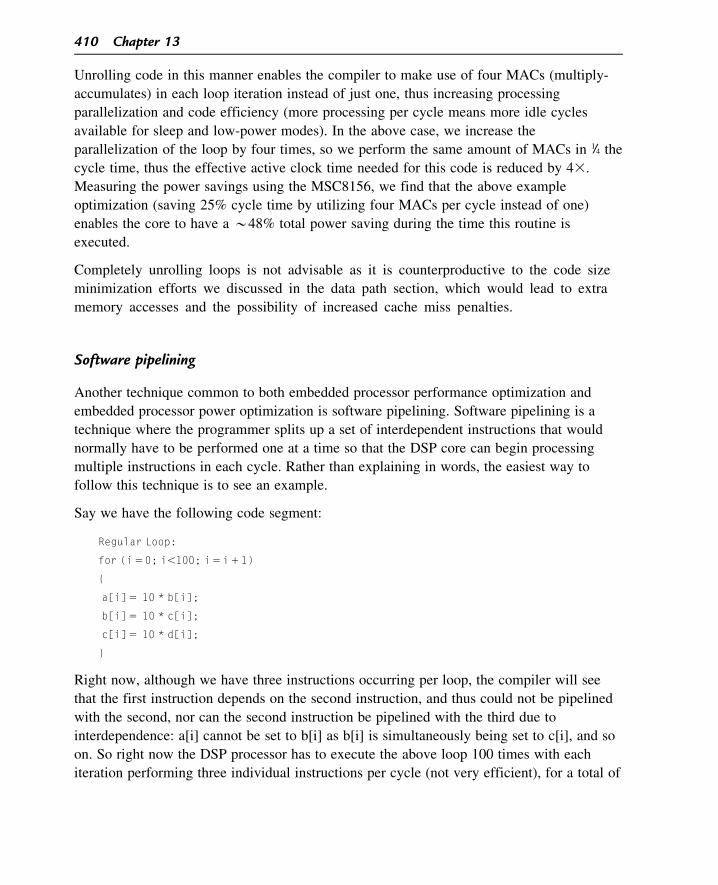
Unrolling code in this manner enables the compiler to make use of four MACs (multiply-
accumulates) in each loop iteration instead of just one, thus increasing processing
parallelization and code efficiency (more processing per cycle means more idle cycles
available for sleep and low-power modes). In the above case, we increase the
parallelization of the loop by four times, so we perform the same amount of MACs in 1/4 the
cycle time, thus the effective active clock time needed for this code is reduced by 43.
Measuring the power savings using the MSC8156, we find that the above example
optimization (saving 25% cycle time by utilizing four MACs per cycle instead of one)
enables the core to have a B48% total power saving during the time this routine is
executed.
Completely unrolling loops is not advisable as it is counterproductive to the code size
minimization efforts we discussed in the data path section, which would lead to extra
memory accesses and the possibility of increased cache miss penalties.
Software pipelining
Another technique common to both embedded processor performance optimization and
embedded processor power optimization is software pipelining. Software pipelining is a
technique where the programmer splits up a set of interdependent instructions that would
normally have to be performed one at a time so that the DSP core can begin processing
multiple instructions in each cycle. Rather than explaining in words, the easiest way to
follow this technique is to see an example.
Say we have the following code segment:
Regular Loop:
for (i50; i,100; i5i11)
{
a[i]5 10 * b[i];
b[i]5 10 * c[i];
c[i]5 10 * d[i];
}
Right now, although we have three instructions occurring per loop, the compiler will see
that the first instruction depends on the second instruction, and thus could not be pipelined
with the second, nor can the second instruction be pipelined with the third due to
interdependence: a[i] cannot be set to b[i] as b[i] is simultaneously being set to c[i], and so
on. So right now the DSP processor has to execute the above loop 100 times with each
iteration performing three individual instructions per cycle (not very efficient), for a total of
410 Chapter 13

300 cycles (best case) performed by MACs in the core of the loop. With software
pipelining, we can optimize this in the following way:
First we see where we can parallelize the above code by unrolling the loop to some extent:
Unrolled loop
a[i]5 10 * b[i];
b[i]5 10 * c[i];
c[i]5 10 * d[i];
a[i11]5 10 * b[i11];
b[i11]5 10 * c[i11];
c[i11]5 10 * d[i11];
a[i12]5 10 * b[i12];
b[i12]5 10 * c[i12];
c[i12]5 10 * d[i12];
a[i13]5 10 * b[i13];
b[i13]5 10 * c[i13];
c[i13]5 10 * d[i13];
Using the above, we can see that certain instructions are not interdependent. The first
assignment of array “a” relies on the original array “b”, meaning we can potentially assign
a entirely before doing any other instructions. If we do this, this means that array “b” would
be entirely free of dependence and could be completely assigned to the original array “c”.
We can abstract this for c as well.
We can use this idea to break the code apart and add parallelism by placing instructions
together that can run in parallel when doing some assignment in advance:
First, we have to perform our first instruction (no parallelism):
a[i]5 10 � b[i];
Then we can have two instructions performed in one cycle:
b[i]5 10 � c[i];a[i1 1]5 10 � b[i1 1];
Here we see that the first and second lines do not depend on each other, so there is no
problem with running the above in parallel as one execution set.
Finally, we reach the point where three instructions in our loop are all being performed in
one cycle:
c[i]5 10 � d[i];b[i1 1]5 10 � c[i1 1];
a[i1 2]5 10 � b[i1 2];
Optimizing Embedded Software for Power 411

Now we see how to parallelize the loop and pipeline, the final software pipelined will first
have some “set-up”, also known as loading the pipeline. This consists of the first sets of
instructions we performed above. After this we have our pipelined loop:
//pipeline loading � first stage
a[i]5 10 * b[i];
//pipeline loading � second stage
b[i]5 10 * c[i];
a[i11]5 10 * b[i11];
//pipelined loop
for (i50; i,100-2; i5i11)
{
c[i]5 10 * d[i];
b[i11]5 10 * c[i11];
a[i12]5 10 * b[i12];
}
//after this, we still have 2 more partial loops:
c[i11]5 10 * d[i11];
b[i12]5 10 * c[i12];
//final partial iteration
c[i12]5 10 * d[i12];
By pipelining the loop, we enabled the compiler to reduce the number of cycles for MACs
from 300 to:
3 MACs that can be performed in 2 cycles for pipeline loading
100 cycles (3 MACs each) in the core of our loop
3 MACs that can be performed in 2 cycles for pipeline loading
for a total of 104 cycles or roughly 1/3 of the execution time, thus reducing the amount of
time the core clocks must be active by 33 for the same functionality! Similar to the loop
unrolling case, the pipelining case has enabled us to save substantially: B43% total power
over the time this routine is executed.
Eliminating recursion
An interesting technique is to eliminate recursive procedure calls in order to reduce
function call overhead.
Recursive procedure calls require the function’s general context, etc., to be pushed onto the
stack with each call. So in the classic case of the factorial example (n!), this can be
calculated using recursion with a function as follows:
412 Chapter 13

fn!ð0Þ5 1 For n55 0
fn!ðnÞ5 fn!ðn2 1Þ; For n. 0
If this recursive factorial function is called with n5 100, there would be B100 function
calls entailing 100 branches to subroutines (which are change of flow routines which affect
the program counter and software stack). Each change of flow instruction takes longer to
execute because not only is the core pipeline disrupted during execution, but every branch
adds at least a return address to the call stack. Additionally, if multiple variables are being
passed, these also must be pushed onto the stack.
This means that this recursive subroutine requires 1003 individual writes to physical
memory and related stall as writes/reads to memory will not be pipelined and 1003
pipeline stalls due to change of flow.
We can optimize this by moving to a simple loop
int res5 1;
for(int i5 0; i, n; i11)
{
res�5 i;
}
This function requires no actual writes to the stack/physical memory as there are no
function calls/jumps. As this function only involves a single multiply, it qualifies as a
“short loop” on certain devices, whereby the loop is entirely handled in hardware.
Thanks to this feature, there are no change of flow penalties, no loop overhead either, so
this effectively acts like a completely unrolled loop of multiplies (minus the memory
cost).
Compared to the recursive routine, using the loop for 100 factorial saves approximately:
• 100 changes of flow (pipeline cycle penalties)
• 1001 pushes to the stack (1003 memory accesses).
For the above example, avoiding recursion savings can be estimated as follows.
The loop method’s change of flow savings from avoiding pipeline disruptions depend on
the pipeline length and if there is any branch prediction available in the core hardware. In
the case of a 12-stage pipeline, refilling it would potentially be a 12-cycle penalty. As
branch target prediction is available on some processors, this may reduce some of this
penalty significantly, but not completely. We can multiply the estimated stall penalty by the
factorial (iteration), which will indicate the additional active core clock cycles and thus
active power consumption from the core due to recursion.
Optimizing Embedded Software for Power 413

Table 13.1: Summary of power-optimization techniques.
Category Technique Impact
Hardwaresupport
Power gating: via a VRM or processor-supported interface, switch offcurrent to specific logic or peripherals of the device
High
Hardwaresupport
Clock gating: often provided as device low-power modes, maximize theamount of clocks that can be shut down for an application
High
Hardwaresupport
Voltage and clock scaling: where available, reduce frequency and voltage. Processordependent
Hardwaresupport
Peripheral low-power modes: gating power/clock to peripherals. Medium-High
Data flow DDR optimizing timing: increasing timing between ACTIVATE commands LowData flow DDR interleaving: used to reduce PRECHARGE/ACTIVATE combinations HighData flow DDR optimization of software organization: organizing buffers to fit into
logical banks to avoid PRECHARGE/ACTIVATE commandsMedium
Data flow DDR general configuration: avoid using modes such as open/closed pagemode, which would force a PRECHARGE/ACTIVATE after each write
High
Data flow DDR burst accesses: organize memory to make full use of the DDR burstsize. This includes alignment and data packing
Medium
Data flow Code size: optimize code and data for minimal size via compiler tools Applicationdependent
Data flow Code size: code packing MediumData flow Code size: creating functions for common tasks Application
dependentData flow Code size: utilized combined function instructions (multiple instructions in
one, which save size and cycles)Processordependent
Data flow Code size: use tools for compression on the fly Processordependent
Data flow Parallelize and pipeline accesses to memory MediumData flow Use constants and avoid zeroing out memory Processor
dependentData flow Cache: layout memory to take advantage of cache set associativity Application
dependentData flow Cache: use write-back model when available and feasible for application Application
dependentData flow Cache: use prefetching to bring data in ahead of time and avoid miss
penalties and extra dead clock cyclesApplicationdependent
Data flow Cache: array merging Applicationdependent
Data flow Cache: interchanging Applicationdependent
Data flow Take advantage of DMA for memory movement MediumData flow Coprocessors: use to perform functions instead of core MediumData flow System bus configuration: configure bus to minimize stalls and bottlenecks Application
dependentData flow Peripheral speed grades and bus width: optimize per usage needs. Application
dependentData flow Peripheral to core flow: use interrupt processing when possible HighAlgorithmic Medium
(Continued)
414 Chapter 13

The cost of recursion causing 1001 individual stack accesses is great, as even in internal
device memory there is potentially an initial delay penalty for initial access. As these stack
accesses will not be pipelined, initial memory delay is multiplied by the number of
recursive calls. If we assume the stack is stored low-latency internal memory running at the
core speed, initial latency could still be seen of the order of anywhere from 8 to 20 cycles.
A 10-cycle latency for initial access would not be a problem if subsequent accesses were
pipelined, meaning 100 reads have a total core stall time of 10 cycles, but in the case of
recursion we have non-pipelined accesses and thus 103 100 stalls, or 1000 additional core
cycles of active clock-consuming power.
In the above example, removing recursion and moving to loops reduces the total energy
(power over time) consumed by the processor to complete the factorial function to less than
half.
Reducing accuracy
Often programmers will over-calculate mathematical functions, using too much accuracy
(too much precision), which can lead to more complicated programs requiring more
functional units and more cycles.
If 16-bit integers could be used as the signal-processing application it is able to tolerate
more noise, but if 32-bit integers are used instead, this could cause additional cycles for just
a basic multiply. A 16-bit by 16-bit multiply can be completed in one cycle on most
architectures, but a 32-bit by 32-bit may require more. Such is the case for the SC3400 DSP
core, which requires two cycles instead of one, so the programmer is doubling the cycle
time for the operation needlessly (inefficient processing and additional clock cycles where
the core is consuming active dynamic power).
Table 13.1: (Continued)
Category Technique Impact
Compiler optimization levels: use compiler optimization tools to optimizefor performance to minimize cycle time in critical areas, and optimize for
code size elsewhereAlgorithmic Instruction packing: maximize code to functionality efficiency MediumAlgorithmic Loop unrolling: maximizes parallelism, minimizes active clock time HighAlgorithmic Software pipelining: another method to maximize parallelism and minimize
active clock timeHigh
Algorithmic Eliminating recursion: save cycle time from function call overhead HighAlgorithmic Reducing accuracy: saving cycles by reducing calculations Application
dependentAlgorithmic Low-power code sequences: using equivalent functions via a lower-power
set of instructionsProcessordependent
Optimizing Embedded Software for Power 415

Low-power code sequences and data patterns
Another suggestion is to look at the specific instructions used for an operation or algorithm.
The programmer may be able to perform exactly the same function with different
commands while saving power, though the analysis and work to do this is very time-
consuming and detail-oriented.
Different instructions activate different functional units, and thus different power
requirements. To accurately use this, it requires the programmer to profile equivalent
instructions to understand the power trade-offs.
Obvious examples could be using a MAC when only the multiply functionality is needed.
Less obvious comparisons, such as the power consumption difference between using a
subtraction to clear a register versus the actual clear instruction, require the programmer to
profile power consumption for each instruction, as we may not know internally how the
hardware goes about clearing a register.
Summary and closing remarks
In order to provide the reader with tools to optimize software for power, over 30 different
optimization techniques in the areas of low power modes, current and voltage controls,
memory optimization, data path optimization, and algorithmic strategies have been
discussed. A summary of those techniques are provided in Table 13.1.
416 Chapter 13