skpm study on organic-inorganic perovskite materialsbmphys.cqu.edu.cn/paper/song2018.pdf · as skpm...
TRANSCRIPT

SKPM study on organic-inorganic perovskite materialsKena Song, Yinghui Wu, Xi Chen, Yi He, Liyu Liu, Guo Chen, and Ruchuan Liu
Citation: AIP Advances 8, 035114 (2018); doi: 10.1063/1.5021755View online: https://doi.org/10.1063/1.5021755View Table of Contents: http://aip.scitation.org/toc/adv/8/3Published by the American Institute of Physics
Articles you may be interested in Ferroelectric, pyroelectric, and piezoelectric properties of a photovoltaic perovskite oxideApplied Physics Letters 110, 063903 (2017); 10.1063/1.4974735
Crystalline orientation dependent photoresponse and heterogeneous behaviors of grain boundaries inperovskite solar cellsJournal of Applied Physics 123, 083105 (2018); 10.1063/1.5007857
Photocharge accumulation and recombination in perovskite solar cells regarding device performance andstabilityApplied Physics Letters 112, 053904 (2018); 10.1063/1.5009040
Unusual defect physics in CH3NH3PbI3 perovskite solar cell absorberApplied Physics Letters 104, 063903 (2014); 10.1063/1.4864778
Mechanical response of CH3NH3PbI3 nanowiresApplied Physics Letters 112, 111901 (2018); 10.1063/1.5023115
Qualifying composition dependent p and n self-doping in CH3NH3PbI3Applied Physics Letters 105, 163508 (2014); 10.1063/1.4899051
AIP ADVANCES 8, 035114 (2018)
SKPM study on organic-inorganic perovskite materialsKena Song, Yinghui Wu, Xi Chen, Yi He, Liyu Liu, Guo Chen,and Ruchuan Liua
Department of Physics, Chongqing University, Chongqing 401331, China
(Received 8 January 2018; accepted 7 March 2018; published online 19 March 2018)
We report Atomic Force Microscopy (AFM) and Scanning Kelvin Probe Microscopy(SKPM) studies on the surface morphology and surface potential propertiesof CH3NH3PbI3, CH3NH3PbI3-xClx, CH3NH3PbI3-xBrx and CH3NH3PbBr3-xClx,respectively. For CH3NH3PbI3 rod structure, its surface potential is independent ofthe precursor concentration, suggesting a robust electronic feature. Surface potentialstudies of CH3NH3PbI3 particle reveal that the Fermi level within CH3NH3PbI3 isstrongly influenced by the substrate. In the case of CH3NH3PbI3-xClx, its surfacepotential depends on precursor concentrations and we suspect that chlorine concen-trated solutions might lead to more chlorine incorporation in the final products, thuslowering its Fermi level. Also, we studied the surface potentials of CH3NH3PbI3-xBrx
and CH3NH3PbBr3-xClxwith specified halide ratios. The surface potential differ-ences between different samples are related to their work function variations. Theseresults are helpful to the understanding of the structural and electronic propertiesof perovskite materials. © 2018 Author(s). All article content, except where oth-erwise noted, is licensed under a Creative Commons Attribution (CC BY) license(http://creativecommons.org/licenses/by/4.0/). https://doi.org/10.1063/1.5021755
I. INTRODUCTION
Since their first introduction in solar cells in 2009,1 methylammonium lead halide perovskitematerials (e.g., CH3NH3PbX3,X = Cl, Br, I) have attracted much attention in photovoltaic researchcommunity.2–9 The power conversion efficiency of perovskite based solar cells has already surpassed20% in a few years.10 Various investigations have revealed their great potential as a prospectivecandidate for photovoltaic application, featuring with favorable bandgap, high absorption coefficient,high carrier mobility and long electron/hole diffusion length.11–14
For iodide/chloride mixed perovskite CH3NH3PbI3-xClx, a variety of experiments are conductedto investigate the role of chlorine element.15–25 It shows that Cl ions in the precursor solution have aprofound and beneficial effect on the film morphology,15,16 carrier transport,13 and stability,17,26 eventhough Cl remains at a very low content in the perovskite lattice.24,25,27,28 For iodide/bromide andchloride/bromide mixed perovskites, their optical and electronic properties can be tuned by changingthe halide ratios.29–31 These perovskites are mostly wide bandgap and are not suitable for photovoltaicapplications due to their transparency to most of the solar spectrum. However, recent studies haveshown promising prospects for their use in light emission devices whose spectral response can bechemically tuned across the entire visible spectrum.30,31
Despite the fast development for perovskite materials, more studies are needed to clearly clarifytheir structure-property relations. Scanning Kelvin Probe Microscopy (SKPM) is a surface potentialdetection technique based on AFM. It measures the surface potential or contact potential difference(VCPD) by compensating the electrostatic forces between the microscopic probe and sample. Thecontact potential difference is generally determined by the effective work function of two materi-als and the electrostatic potential difference. The former depends on the surface properties of thetwo materials, and the latter is determined by the bias and surface charges of the sample.32 SKPM
aEmail: [email protected]
2158-3226/2018/8(3)/035114/12 8, 035114-1 © Author(s) 2018
035114-2 Song et al. AIP Advances 8, 035114 (2018)
is widely used in multiple disciplines to study the morphology and surface electronic properties ofmaterials simultaneously.33–35 It also has been used for perovskite films to study grain boundary (GB)effects.36–40 Their SKPM studies revealed a downward band bending in the energy band diagram atthe GBs which act as effective charge dissociation interfaces and photocurrent transduction path-ways, enhance minority carrier collection and boost the overall performance of the device. However,as SKPM directly gives the local work function/Fermi level of materials, or at least shows the relativeenergy levels with careful controls on experimental conditions in air, it provides a useful approachto obtain insights on the electronic properties of perovskite and the interaction between perovskitematerials and substrates.
In this work, we systematically conduct AFM and SKPM experiments to investigate themorphology and surface potential of CH3NH3PbI3, CH3NH3PbI3-xClx, CH3NH3PbI3-xBrx andCH3NH3PbBr3-xClx, respectively. For triiodide perovskite, two different structures are formed.The rod structure is made by single-step pre-mixed precursor deposition, particle structure bytwo-step deposition. The concentration effect and substrate effect on the energy barrier at theperovskite/substrate interfaces are studied. Then by studying CH3NH3PbI3-xClx perovskite filmsdeposited from three precursor concentrations, we establish a connection between its Fermi leveland chlorine effect. Also, we studied the surface potential of I/Br and Br/Cl mixed perovskites withspecified ratios and the surface potential is correlated with their work functions.
II. RESULT AND DISCUSSION
A. Morphology and surface potential study of CH3NH3PbI3We first choose to investigate the most widely studied perovskite CH3NH3PbI3.1 Structures are
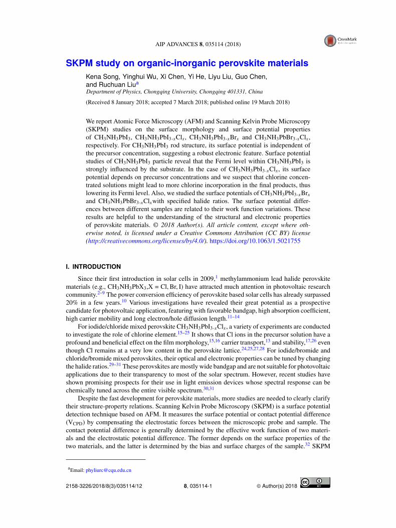
both formed by solution approaches. The common rod structure is made by one-step pre-mixed pre-cursor deposition, and the particle structure by two-step deposition. Their typical topography imagesare shown in Figures 1(a) and 1(b), respectively. Four precursor solutions with different concentra-tions are used to obtain perovskite rods with micrometer-long sizes. Increasing concentration from4.8 to 29 wt%, the rod length grows from ∼4.5 µm to ∼20 µm and its average height increasesfrom 5.8 nm to 211.7 nm. For particle perovskite, FTO, PEDOT:PSS/FTO and PEDOT:PSS/glass areused as substrates. The size distributions of obtained rods and particles are summarized in Table I.More topography images can be found in the supplementary material(Figure S1, S4).
Figures 1(g) and 1(h) shows the absorption spectra and PL spectra of both perovskite particlesand rods, respectively. Perovskite particles show more pronounced absorption peaks around 420 nmand 500 nm. The absorption spectra of the both structures display a distinct absorption onset aroundthe energy band gap (∼760 nm), indicating the formation of perovskite. This is also confirmed by theirsteady state PL spectra, which show emission peaks around 764 nm. A slight shift in the emissionpeak (∼756 nm) is observed for rod perovskite.
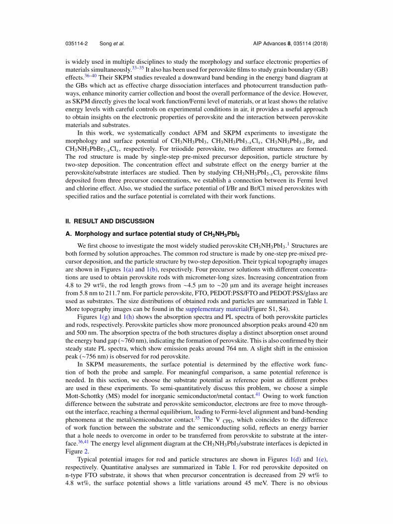
In SKPM measurements, the surface potential is determined by the effective work func-tion of both the probe and sample. For meaningful comparison, a same potential reference isneeded. In this section, we choose the substrate potential as reference point as different probesare used in these experiments. To semi-quantitatively discuss this problem, we choose a simpleMott-Schottky (MS) model for inorganic semiconductor/metal contact.41 Owing to work functiondifference between the substrate and perovskite semiconductor, electrons are free to move through-out the interface, reaching a thermal equilibrium, leading to Fermi-level alignment and band-bendingphenomena at the metal/semiconductor contact.35 The V CPD, which coincides to the differenceof work function between the substrate and the semiconducting solid, reflects an energy barrierthat a hole needs to overcome in order to be transferred from perovskite to substrate at the inter-face.36,41 The energy level alignment diagram at the CH3NH3PbI3/substrate interfaces is depicted inFigure 2.
Typical potential images for rod and particle structures are shown in Figures 1(d) and 1(e),respectively. Quantitative analyses are summarized in Table I. For rod perovskite deposited onn-type FTO substrate, it shows that when precursor concentration is decreased from 29 wt% to4.8 wt%, the surface potential shows a little variations around 45 meV. There is no obvious

035114-3 Song et al. AIP Advances 8, 035114 (2018)
FIG. 1. Topography, surface potential and optical properties of perovskites. (a-c) AFM topography images of rodCH3NH3PbI3, particle CH3NH3PbI3 and CH3NH3PbI3-xClx deposited on FTO substrate, respectively. (d-f) Correspond-ing contact potential difference obtained by SKPM. (g) Similar absorption spectra both display a distinct absorption onsetaround 760 nm, indicating the formation of final perovskites. (h) PL spectra of rod CH3NH3PbI3 and CH3NH3PbI3-xClxshare a nearly identical emission peak around 750 nm. A slight shift in the emission peak (∼756 nm) is observed for rodCH3NH3PbI3.
connections between the surface potential and the rod size. This suggests that the electronic propertiesof this rod structure perovskite is robust or that CH3NH3PbI3 is defect tolerance as small variationsin the processing/reaction could lead to an incomplete conversion or structural heterogeneity acrossthe bulk film, resulting defects or different phases in perovskite films. The topography and poten-tial images of these rods made from these precursor solutions are shown in supplementary material(Figure S1, S2, S3).
The surface potential of particle perovskite depends on the substrates used. On the n-type FTOsubstrate, SKPM measurement exhibits an energy barrier around 11 meV. When another p-typePEDOT:PSS film is spin coated on FTO or glass substrates before the perovskite deposition, thebarrier is lowered to around 0∼4 meV. These results agree with literature which reveals that the Fermilevel within CH3NH3PbI3 is strongly influenced by the substrate.42 The n-type substrates (FTO usedhere) yield strongly n-type surfaces, while the p-type substrates (PEDOT:PSS used here) result inperovskite surfaces that are more p-type like. The small potential difference at perovskite/PEDOT:PSSinterface indicates that their Fermi levels are very close before reaching equilibrium as depicted inFigure 2.
B. Morphology and surface potential study of CH3NH3PbI3-xClxIodide/chloride mixed perovskite (CH3NH3PbI3-xClx) is another widely used perovskite.
It possesses the same basic crystalline structure and similar electronic structure as its CH3NH3PbI3
035114-4 Song et al. AIP Advances 8, 035114 (2018)
TABLE I. Summarized potential of rod CH3NH3PbI3, particle CH3NH3PbI3 and CH3NH3PbI3-xClx , together with theirheight and size distribution.
Comparison Surface potential Height (nm) Size (nm)conditions (meV) avg± std avg± std avg± std
CH3NH3PbI3 roda 29.0 wt% -45.9± 16.8 211.7± 137.9 20177.5± 6208.421.4 wt% -36.9± 11.9 116.3± 202.7 15861.2± 3248.56.3 wt% -51.6± 17.0 17.9± 16.7 6462.9± 2021.14.8 wt% -45.1± 17.3 5.8± 11.4 4526.1± 1310.8
CH3NH3PbI3 Particleb FTO -11.4± 12.3 200.6± 49.9 474.8± 329.2PEDOT/FTO -4.9± 8.5 220.8± 25.8 568.6± 120.3PEDOT/glass 0.0± 5.4 107± 11.1 400.7± 81.1
CH3NH3PbI3-xClxc 32.9 wt% -174.6± 27.7 143.6± 144.5 -24.7 wt% -71.4± 17.3 100.9± 97.4 -7.6 wt% -23.6± 9.2 77.8± 97.6 -
aPrecursor solutions with concentrations ranging from 4.8 wt% to 29 wt% are used to form different sized rod CH3NH3PbI3.bParticle CH3NH3PbI3 is formed on n-type FTO substrate and p-type PEDOT:PSS films, repectively.cThe CH3NH3PbI3-xClx film is spin coated from precursor solutions with concentrations of 32.9 wt%, 24.7 wt% and 7.6 wt%, respectively.
analogue.28,43 However, its carrier lifetime and diffusion length are found to increase by morethan an order of magnitude.13 For example, experiment shows that electron-hole diffusion lengthsin CH3NH3PbI3-xClx exceed 1 µm compared with ∼100 nm in CH3NH3PbI3. In this section,we study the film morphology and surface potential of CH3NH3PbI3-xClx by AFM and SKPM,respectively.
The CH3NH3PbI3-xClx films are deposited by spin coating a precursor solution with respective32.9 wt%, 24.7 wt% and 7.6 wt% concentrations. Its typical topography and surface potential imagesare compared with CH3NH3PbI3 rod in Figure 1. More topography and potential images can befound in supplementary material (Figure S7). Figures 1(g) and 1(h) shows that these two perovskitesshare nearly identical absorption and PL spectra. However, their topography images are different.Instead of the rod structure made by one-step method for CH3NH3PbI3, the structure ofCH3NH3PbI3-xClx is mainly isolated fused-like crystalline islands with several micrometer in sizeat least. It is caused by their different crystal growth kinetics. It is reported that the PbCl2 additionaffected perovskite crystal formation kinetics by acting as heterogeneous nucleation sites due to itslimited solubility in DMF.44
The surface potential of CH3NH3PbI3-xClx are also different compared with CH3NH3PbI3.From the SKPM measurements, its surface potential depends on the concentrations of the precur-sor used. The surface potential data are summarized in Table I. Its surface potential decreases from175 meV for 32.9 wt% solution to 71 meV and 24 meV for 24.7 wt% and 7.6 wt% solution, respec-tively. This indicates that its Fermi level is lowered with the increasing precursor concentrations.
FIG. 2. Energy diagram of CH3NH3PbI3 on n-type or p-type substrates before and after contact. (a) N-type substrates (FTO)yield strongly n-type CH3NH3PbI3. (b) P-type substrates (PEDOT:PSS) result in p-type like CH3NH3PbI3. After contact,electrons are free to move across the interface, leading to Fermi-level alignment and band-bending at the metal/semiconductorcontact according to Mott–Schottky model.
035114-5 Song et al. AIP Advances 8, 035114 (2018)
By comparing their topography and potential line profiles in Figure S9 in supplementary material,the potential variation is not following its height variation. Thus, the contribution of the substrate tothe potential data is neglected.
Here, we speculate that the dependence of surface potential on the precursor concentrationsmight be related to the presence of chloride in perovskite films. It is expected that more chlorineconcentrated solutions might lead to more chlorine incorporation although the content is very low,thus lowering its Fermi level. In a previous study about As-doped CdTe, SKPM experiments revealedthat increasing As concentrations in CdTe led to a decrease in V CPD, a downward shift in the CdTeFermi level and an increase in the CdTe work function.45 We would expect the same case here.It is also consistent with a recent literature about CH3NH3PbI3(Cl)-based perovskite solar cellswhich found that chlorine incorporation decreased the V CPD compared with CH3NH3PbI3, resultinga lower Fermi level.43 XPS and UPS experiments also confirmed that CH3NH3PbI3-xClx has a slighthigher work function than CH3NH3PbI3.46 More topography and surface potential can be found inthe supplementary material (Figure S7, S8, S9).
C. Morphology and optical properties of I/Br mixed perovskite films
For CH3NH3PbI3-xClx perovskite, the chlorine element is believed to be at a very low concen-tration.24,25,27,28 It is caused by the limited chloride solubility in the iodide derivative due to thelarge difference in the ionic radii of ClandI anions.24 However, for I/Br and Cl/Br mixed perovskites,the composition can be widely tuned from 0 ∼1 by varying the halide ratio in the precursor solu-tion.29–31 Similar conclusions were drawn for other halide compounds, such as CH3NH3SnX3,47
CH3NH3I1-xBrx and CH3NH3Br1-xClx (Figure S10 in supplementary material).I/Br mixed perovskites CH3NH3Pb(I1-xBrx)3 are deposited by spin coating precursors with
specified CH3NH3I/CH3NH3Br ratios mixed with PbAc2 in DMF solvent. As the halide element
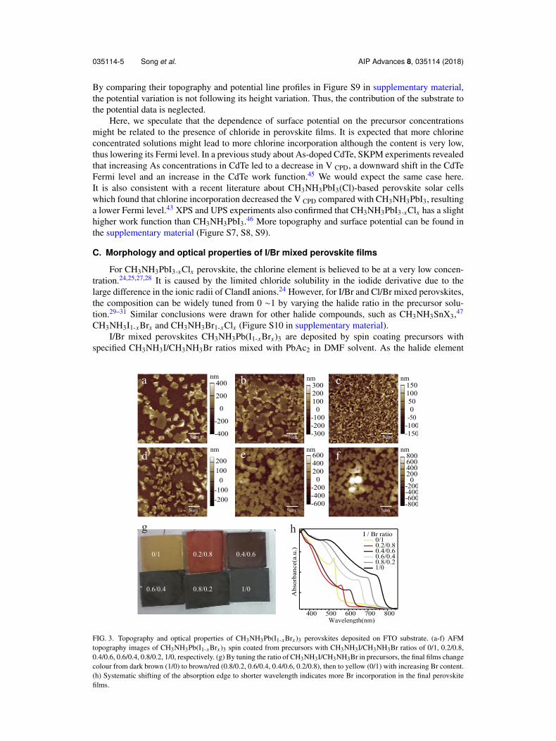
FIG. 3. Topography and optical properties of CH3NH3Pb(I1-xBrx)3 perovskites deposited on FTO substrate. (a-f) AFMtopography images of CH3NH3Pb(I1-xBrx)3 spin coated from precursors with CH3NH3I/CH3NH3Br ratios of 0/1, 0.2/0.8,0.4/0.6, 0.6/0.4, 0.8/0.2, 1/0, respectively. (g) By tuning the ratio of CH3NH3I/CH3NH3Br in precursors, the final films changecolour from dark brown (1/0) to brown/red (0.8/0.2, 0.6/0.4, 0.4/0.6, 0.2/0.8), then to yellow (0/1) with increasing Br content.(h) Systematic shifting of the absorption edge to shorter wavelength indicates more Br incorporation in the final perovskitefilms.
035114-6 Song et al. AIP Advances 8, 035114 (2018)
comes only from the CH3NH3I/CH3NH3Br mixtures, Pb source from PbAc2, the final perovskitecomposition are more easily controlled. Studies also show that the PbAc2 are facilitating theremoval of the by-products during crystallization, thus obtaining more continuous films with lesspinholes.48
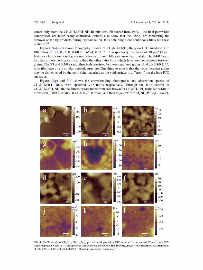
Figures 3(a)–3(f) shows topography images of CH3NH3Pb(I1-xBrx)3 on FTO substrate withI/Br ratios of 0/1, 0.2/0.8, 0.4/0.6, 0.6/0.4, 0.8/0.2, 1/0,respectively, for areas of 30 µm*30 µm.It shows a little variation of grain size between different I/Br ratio mixed perovskite. The 0.4/0.6 ratiofilm has a more compact structure than the other ratio films which have less connections betweengrains. The 0/1 and 0.2/0.8 ratio films both consisted by more separated grains. And the 0.8/0.2, 1/0ratio film have a very similar network structure. One thing to note is that the voids between grainsmay be also covered by the perovskite materials as the void surface is different from the bare FTOsubstrate.
Figures 3(g) and 3(h) shows the corresponding photographs and absorption spectra ofCH3NH3Pb(I1-xBrx)3 with specified I/Br ratios respectively. Through the ratio control ofCH3NH3I/CH3NH3Br, the film colors are tuned from dark brown for CH3NH3PbI3 (ratio I/Br=1/0) tobrown/red (0.8/0.2, 0.6/0.4, 0.4/0.6, 0.2/0.8 ratios) and then to yellow for CH3NH3PbBr3(I/Br=0/1)
FIG. 4. SKPM results of CH3NH3Pb(I1-xBrx)3 perovskites deposited on FTO substrate for an area of 5∗5µm2. (a-f) AFMsurface topography and (g-l) Corresponding surface potential maps of CH3NH3Pb(I1-xBrx)3 with CH3NH3I/CH3NH3Br ratioof 0/1, 0.2/0.8, 0.4/0.6, 0.6/0.4, 0.8/0.2, 1/0 used in precursors, respectively.
035114-7 Song et al. AIP Advances 8, 035114 (2018)
TABLE II. Average potential of CH3NH3Pb(I1-xBrx)3 perovskites for an area of 5µm*5µm with indicatedCH3NH3I/CH3NH3Br ratio used in precursor solutions. The standard deviation (STD) reflects the local work functioninhomogeneities.
Sample number CH3NH3I/CH3NH3Br ratio Surface potential (meV) STD
1 0/1 -172 40.62 0.2/0.8 -135 35.93 0.4/0.6 -61 7.94 0.6/0.4 31 3.25 0.8/0.2 -2 2.96 1/0 -123 3.6
with increasing Br content. A systematic shift of the absorption band edge to shorter wavelength withincreasing Br content in CH3NH3Pb(I1-xBrx)3 indicates the incorporation of Br element, resultingin the energy band gap (Eg) changes. Also notes that samples with higher Br content (ratio 0/1 and0.2/0.8) exhibit a peak at the absorption edge that is related to an excitonic transition that appearsdue to the higher exciton binding energy at high Br concentration.49
D. Surface potential study of I/Br mixed perovskite films
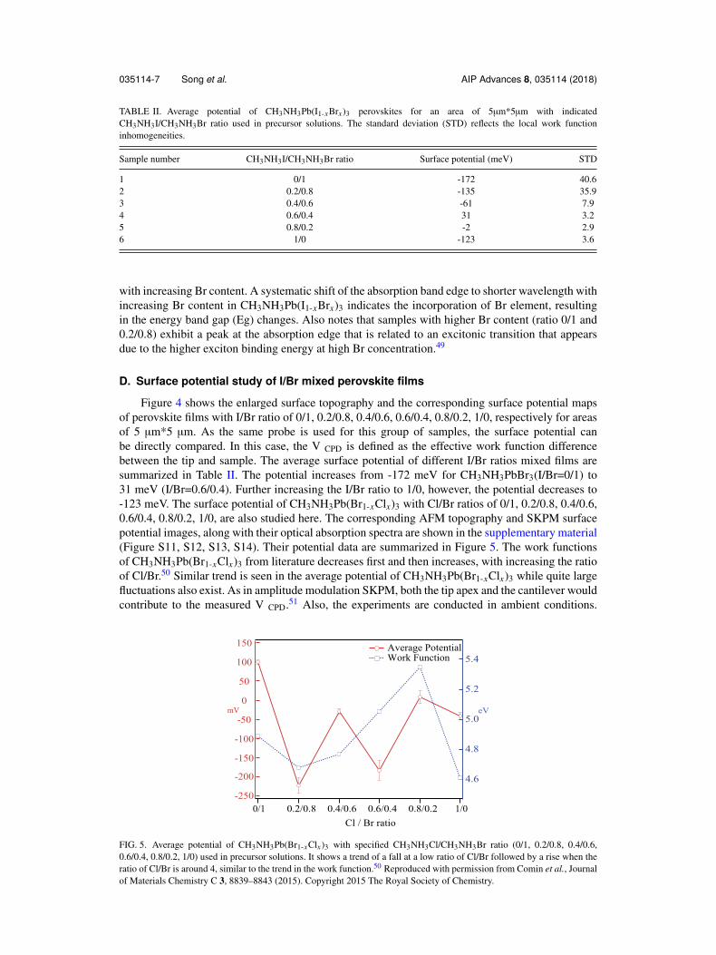
Figure 4 shows the enlarged surface topography and the corresponding surface potential mapsof perovskite films with I/Br ratio of 0/1, 0.2/0.8, 0.4/0.6, 0.6/0.4, 0.8/0.2, 1/0, respectively for areasof 5 µm*5 µm. As the same probe is used for this group of samples, the surface potential canbe directly compared. In this case, the V CPD is defined as the effective work function differencebetween the tip and sample. The average surface potential of different I/Br ratios mixed films aresummarized in Table II. The potential increases from -172 meV for CH3NH3PbBr3(I/Br=0/1) to31 meV (I/Br=0.6/0.4). Further increasing the I/Br ratio to 1/0, however, the potential decreases to-123 meV. The surface potential of CH3NH3Pb(Br1-xClx)3 with Cl/Br ratios of 0/1, 0.2/0.8, 0.4/0.6,0.6/0.4, 0.8/0.2, 1/0, are also studied here. The corresponding AFM topography and SKPM surfacepotential images, along with their optical absorption spectra are shown in the supplementary material(Figure S11, S12, S13, S14). Their potential data are summarized in Figure 5. The work functionsof CH3NH3Pb(Br1-xClx)3 from literature decreases first and then increases, with increasing the ratioof Cl/Br.50 Similar trend is seen in the average potential of CH3NH3Pb(Br1-xClx)3 while quite largefluctuations also exist. As in amplitude modulation SKPM, both the tip apex and the cantilever wouldcontribute to the measured V CPD.51 Also, the experiments are conducted in ambient conditions.
FIG. 5. Average potential of CH3NH3Pb(Br1-xClx)3 with specified CH3NH3Cl/CH3NH3Br ratio (0/1, 0.2/0.8, 0.4/0.6,0.6/0.4, 0.8/0.2, 1/0) used in precursor solutions. It shows a trend of a fall at a low ratio of Cl/Br followed by a rise when theratio of Cl/Br is around 4, similar to the trend in the work function.50 Reproduced with permission from Comin et al., Journalof Materials Chemistry C 3, 8839–8843 (2015). Copyright 2015 The Royal Society of Chemistry.
035114-8 Song et al. AIP Advances 8, 035114 (2018)
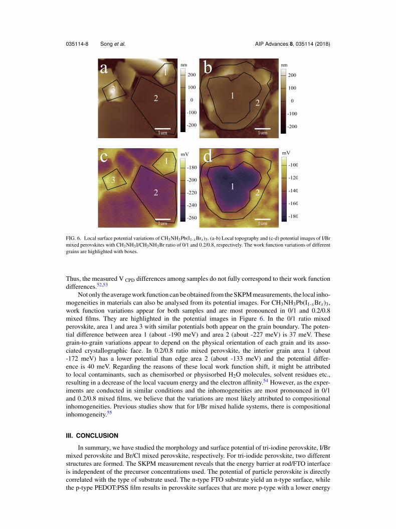
FIG. 6. Local surface potential variations of CH3NH3Pb(I1-xBrx)3. (a-b) Local topography and (c-d) potential images of I/Brmixed perovskites with CH3NH3I/CH3NH3Br ratio of 0/1 and 0.2/0.8, respectively. The work function variations of differentgrains are highlighted with boxes.
Thus, the measured V CPD differences among samples do not fully correspond to their work functiondifferences.52,53
Not only the average work function can be obtained from the SKPM measurements, the local inho-mogeneities in materials can also be analysed from its potential images. For CH3NH3Pb(I1-xBrx)3,work function variations appear for both samples and are most pronounced in 0/1 and 0.2/0.8mixed films. They are highlighted in the potential images in Figure 6. In the 0/1 ratio mixedperovskite, area 1 and area 3 with similar potentials both appear on the grain boundary. The poten-tial difference between area 1 (about -190 meV) and area 2 (about -227 meV) is 37 meV. Thesegrain-to-grain variations appear to depend on the physical orientation of each grain and its asso-ciated crystallographic face. In 0.2/0.8 ratio mixed perovskite, the interior grain area 1 (about-172 meV) has a lower potential than edge area 2 (about -133 meV) and the potential differ-ence is 40 meV. Regarding the reasons of these local work function shift, it might be attributedto local contaminants, such as chemisorbed or physisorbed H2O molecules, solvent residues etc.,resulting in a decrease of the local vacuum energy and the electron affinity.54 However, as the exper-iments are conducted in similar conditions and the inhomogeneities are most pronounced in 0/1and 0.2/0.8 mixed films, we believe that the variations are most likely attributed to compositionalinhomogeneities. Previous studies show that for I/Br mixed halide systems, there is compositionalinhomogeneity.55
III. CONCLUSION
In summary, we have studied the morphology and surface potential of tri-iodine perovskite, I/Brmixed perovskite and Br/Cl mixed perovskite, respectively. For tri-iodide perovskite, two differentstructures are formed. The SKPM measurement reveals that the energy barrier at rod/FTO interfaceis independent of the precursor concentrations used. The potential of particle perovskite is directlycorrelated with the type of substrate used. The n-type FTO substrate yield an n-type surface, whilethe p-type PEDOT:PSS film results in perovskite surfaces that are more p-type with a lower energy
035114-9 Song et al. AIP Advances 8, 035114 (2018)
barrier. For chloride mixed perovskite, measurements show the energy barrier is decreased from175 meV to 71 meV and 24 meV for 32.9 wt%, 24.7 wt% and 7.6 wt%, respectively. It is expectedthat chlorine concentrated solutions might lead to more chlorine incorporation, thus lowering itsFermi level. Also, we studied the surface potential of I/Br and Br/Cl mixed perovskites with spec-ified ratios. The surface potential trend between samples is directly related to their work functions.We believe these studies are helpful to understand the structural, optical and electronic properties ofperovskite materials.
IV. EXPERIMENTAL
A. Materials
All the chemicals were purchased from Aladdin Inc unless specified and were used as receivedwithout further purification, including HI (55-58 wt% in water), HBr(ACS, 48 wt%), HCl(36-38%),CH3NH2(AR, 30-33 wt% in absolute ethanol), PbI2(99.9% metals basis),PbCl2(99.99% metals basis),Pb(Ac)2 ·3H2O (99.99% metals basis), N,N-dimethylformamide (GC, > 99.9%), Isopropyl Alcohol(AR, ≥ 99.5%), diethyl ether (AR), ethanol (ACS, ≥ 99.5%), acetone (AR). PEDOT:PSS (CleviosPH 1000) was purchased from H.C.Starck.
1. Methylammonium halide synthesis
Methylammonium halide (CH3NH3I,CH3NH3Br,CH3NH3Cl) was synthesized by the reactionof methylamine aqueous solution and the corresponding hydrohalide (HCl,HBr,HI) acid in a beaker atroom temperature for 2 h with constant stirring. The precipitate was recovered by carefully evaporatingthe solvents at 70 ◦C. The raw product CH3NH3X was then rinsed with diethyl ether and dried at60 ◦C in a vacuum oven overnight.
Methylammonium mix halides (CH3NH3I1-xBrx and CH3NH3I1-xClx) were synthesized by evap-orating the specified ratio of CH3NH3I(CH3NH3Cl) and CH3NH3Br in ethanol solution at 70 ◦C.The raw product was rinsed with diethyl ether and dried at 60 ◦C in a vacuum oven overnight.
B. Precursor preparation and film formation
Before the film deposition, FTO coated glass substrates and glass substrates were cleaned withDI water, acetone and ethanol, for 10 min successively in ultra sonicator. Then the substrates wererinsed by DI water and dried with clean air.
To deposit tri-iodide perovskite rod, CH3NH3I powder and PbI2 were dissolved in DMF at 1:1 molar ratio with required concentrations. The obtained solution was stirred overnight before use.Then the precursor was spin coated on FTO substrate at the rotation speed of 3000 rpm for 40 s.The film was finally annealed at 100 ◦C for 30 min on the hotplate.
To deposit tri-iodide perovskite particle, CH3NH3I powder and PbI2 were dissolved in IPA andDMF with a concentration of 30 mg/ml and 100 mg/ml, respectively. For FTO substrate based sample,hot PbI2 precursor solution (70 ◦C) was directly spin coated on FTO surface at a rotation speed of2000 rpm for 40 s without further annealing. For PEDOT:PSS/FTO or PEDOT:PSS/glass substratebased samples, PEDOT:PSS solution was first spin coated on the FTO or glass substrate at a rotationspeed of 2000 rpm for 40 s, followed by annealing at 130 ◦C for 15 min. Then the hot PbI2 precursorsolution (70 ◦C) was spin coated on the PEDOT:PSS surface at a rotation speed of 2000 rpm for40 s. After that, the prepared CH3NH3I solutions were spin coated on FTO, PEDOT:PSS/FTO andPEDOT:PSS/glass substrates at a rotation speed of 2000 rpm for 40 s. During another spin process,several IPA drops were dripped on the films to clean extra CH3NH3I solutions. The obtained filmswere finally annealed at 100 ◦C for 30 min.
For chloride mixed perovskite, CH3NH3I powder and PbCl2 were dissolved in DMF at 3: 1 molarratio with required concentrations. The obtained solution was stirred overnight before use. Then theprecursor was spin coated on FTO substrate at a rotation speed of 3000 rpm for 40 s. The film wasfinally annealed at 100 ◦C for 45 min.
To prepare I/Br and Cl/Br mixed perovskite films, specified CH3NH3I(or CH3NH3Cl)/CH3NH3Brratios and PbAc2 were dissolved in DMF at 3:1 molar ratio at ∼40 wt% concentrations. The obtained
035114-10 Song et al. AIP Advances 8, 035114 (2018)
solutions were stirred overnight before use. Then the precursors were spin coated on FTO substrateat a rotation speed of 3000 rpm for 40 s. The films were finally annealed at 100 ◦C for 10 min.
C. UV-Vis characterization
A UV-3600 spectrophotometer (Shimadzu, Japan) was used for the absorption spectra of samples.PL spectra were recorded by a commercial Micro Raman spectrometer (Horiba), using an excitationlaser beam with a wavelength of 532 nm.
D. Morphology and surface potential characterization
SKPM is implemented on an AFM platform (MFP-3D-BIO, Asylum Research). The measure-ment is carried out in a two-pass technique. The first pass is conducted as a standard AC mode scanand is used to record the surface topography. In the second pass, the tip is then retraced from thefirst topography scan with an additional z distance of 10 ∼50 nm. An AC voltage at a frequency of60-65 kHz and a tunable DC voltage are applied between the tip and the substrate in the second pass.The DC voltage is adjusted at each point to cancel the force at the AC frequency, and accordingly thevalue is recorded as the potential difference. In this article, Pt/Cr coated silicon tips (Multi75E-G,Budget sensor) are used. It has an oscillation frequency of 60 kHz, spring constant of 1-5 N/m, anda quality factor Q of ∼186. All experiments are conducted in ambient conditions, in dark.
SUPPLEMENTARY MATERIAL
See supplementary material for the detailed data.
ACKNOWLEDGMENTS
This work was supported by the National Natural Science Foundation of China (Grant No.11474345, No. 11674043).1 A. Kojima, K. Teshima, Y. Shirai, and T. Miyasaka, “Organometal halide perovskites as visible-light sensitizers for
photovoltaic cells,” Journal of the American Chemical Society 131, 6050–6051 (2009).2 J. Im, C. Lee, J. Lee, S. Park, and N. Park, “6.5% efficient perovskite quantum-dot-sensitized solar cell,” Nanoscale 3,
4088–4093 (2011).3 H. Kim, C. Lee, J. Im, K. Lee, T. Moehl, A. Marchioro, S. Moon, R. Humphrybaker, J. Yum, J. Moser et al., “Lead iodide
perovskite sensitized all-solid-state submicron thin film mesoscopic solar cell with efficiency exceeding 9%,” ScientificReports 2, 591 (2012).
4 M. M. Lee, J. Teuscher, T. Miyasaka, T. N. Murakami, and H. J. Snaith, “Efficient hybrid solar cells based on meso-superstructured organometal halide perovskites,” Science 338, 643–647 (2012).
5 H. Zhou, Q. Chen, G. Li, S. Luo, T. Song, H. Duan, Z. Hong, J. You, Y. Liu, and Y. Yang, “Interface engineering of highlyefficient perovskite solar cells,” Science 345, 542–546 (2014).
6 M. Yang, Y. Zhou, Y. Zeng, C. Jiang, N. P. Padture, and K. Zhu, “Square-centimeter solution-processed planar CH3NH3PbI3perovskite solar cells with efficiency exceeding 15%,” Advanced Materials 27, 6363–6370 (2015).
7 J. H. Heo, D. H. Song, H. J. Han, S. Y. Kim, J. H. Kim, D. Kim, H. W. Shin, T. K. Ahn, C. Wolf, T. Lee et al., “PlanarCH3NH3PbI3 perovskite solar cells with constant 17.2% average power conversion efficiency irrespective of the scan rate,”Advanced Materials 27, 3424–3430 (2015).
8 N. J. Jeon, J. H. Noh, W. S. Yang, Y. C. Kim, S. Ryu, J. Seo, and S. I. Seok, “Compositional engineering of perovskitematerials for high-performance solar cells,” Nature 517, 476–480 (2015).
9 N. Ahn, D. Son, I. Jang, S. M. Kang, M. Choi, and N. Park, “Highly reproducible perovskite solar cells with averageefficiency of 18.3% and best efficiency of 19.7% fabricated via Lewis base adduct of lead(II) iodide,” Journal of theAmerican Chemical Society 137, 8696–8699 (2015).
10 W. S. Yang, J. H. Noh, N. J. Jeon, Y. C. Kim, S. Ryu, J. Seo, and S. I. Seok, “High-performance photovoltaic perovskitelayers fabricated through intramolecular exchange,” Science 348, 1234–1237 (2015).
11 W. Yin, T. Shi, and Y. Yan, “Unique properties of halide perovskites as possible origins of the superior solar cell performance,”Advanced Materials 26, 4653–4658 (2014).
12 C. Wehrenfennig, G. E. Eperon, M. B. Johnston, H. J. Snaith, and L. M. Herz, “High charge carrier mobilities and lifetimesin organolead trihalide perovskites,” Advanced Materials 26, 1584–1589 (2014).
13 S. D. Stranks, G. E. Eperon, G. Grancini, C. Menelaou, M. J. P. Alcocer, T. Leijtens, L. M. Herz, A. Petrozza, and H. J. Snaith,“Electron-hole diffusion lengths exceeding 1 micrometer in an organometal trihalide perovskite absorber,” Science 342,341–344 (2013).
14 G. Xing, N. Mathews, S. Sun, S. S. Lim, Y. M. Lam, M. Gratzel, S. G. Mhaisalkar, and T. C. Sum, “Long-range balancedelectron- and hole-transport lengths in organic-inorganic CH3NH3PbI3,” Science 342, 344–347 (2013).
15 S. T. Williams, F. Zuo, C. Chueh, C. Liao, P. Liang, and A. K. Y. Jen, “Role of chloride in the morphological evolution oforgano-lead halide perovskite thin films,” ACS Nano 8, 10640–10654 (2014).

035114-11 Song et al. AIP Advances 8, 035114 (2018)
16 H. Yu, F. Wang, F. Xie, W. Li, J. Chen, and N. Zhao, “The role of chlorine in the formation process of “CH3NH3PbI3-xClx”perovskite,” Advanced Functional Materials 24, 7102–7108 (2014).
17 J. Chae, Q. Dong, J. Huang, and A. Centrone, “Chloride incorporation process in CH3NH3PbI3-xClx perovskites viananoscale bandgap maps,” Nano Letters 15, 8114–8121 (2015).
18 S. Colella, E. Mosconi, G. Pellegrino, A. Alberti, V. L. P. Guerra, S. Masi, A. Listorti, A. Rizzo, G. G. Condorelli,F. De Angelis et al., “Elusive presence of chloride in mixed halide perovskite solar cells,” Journal of Physical ChemistryLetters 5, 3532–3538 (2014).
19 M. I. Dar, N. Arora, P. Gao, S. Ahmad, M. Gratzel, and M. K. Nazeeruddin, “Investigation regarding the role of chlo-ride in organic–inorganic halide perovskites obtained from chloride containing precursors,” Nano Letters 14, 6991–6996(2014).
20 J. Liu and O. V. Prezhdo, “Chlorine doping reduces electron–hole recombination in lead iodide perovskites: Time-domainab initio analysis,” Journal of Physical Chemistry Letters 6, 4463–4469 (2015).
21 J. Qing, H. T. Chandran, Y. Cheng, X. Liu, H. Li, S. Tsang, M. Lo, and C. S. Lee, “Chlorine incorporation for enhancedperformance of planar perovskite solar cell based on lead acetate precursor,” ACS Applied Materials & Interfaces 7,23110–23116 (2015).
22 E. L. Unger, A. R. Bowring, C. J. Tassone, V. L. Pool, A. Goldparker, R. Cheacharoen, K. H. Stone, E. T. Hoke, M. F. Toney,and M. D. Mcgehee, “Chloride in lead chloride-derived organo-metal halides for perovskite-absorber solar cells,” Chemistryof Materials 26, 7158–7165 (2014).
23 Q. Wang, M. Lyu, M. Zhang, J. H. Yun, H. Chen, and L. Wang, “Transition from the tetragonal to cubic phase of organohalideperovskite: The role of chlorine in crystal formation of CH3NH3PbI3 on TiO2 substrates,” Journal of Physical ChemistryLetters 6, 150929151618007 (2015).
24 S. Colella, E. Mosconi, P. Fedeli, A. Listorti, F. Gazza, F. Orlandi, P. Ferro, T. Besagni, A. Rizzo, G. Calestani et al.,“MAPbI3-xClx mixed halide perovskite for hybrid solar cells: The role of chloride as dopant on the transport and structuralproperties,” Chemistry of Materials 25, 4613–4618 (2013).
25 V. L. Pool, A. Goldparker, M. D. Mcgehee, and M. F. Toney, “Chlorine in PbCl2-derived hybrid-perovskite solar absorbers,”Chemistry of Materials 27, 7240–7243 (2015).
26 Y. Chen, T. Chen, and L. Dai, “Layer-by-layer growth of CH3NH3PbI3-xClx for highly efficient planar heterojunctionperovskite solar cells,” Advanced Materials 27, 1053–1059 (2015).
27 G. Grancini, S. Marras, M. Prato, C. Giannini, C. Quarti, F. De Angelis, M. De Bastiani, G. E. Eperon, H. J. Snaith, L. Mannaet al., “The impact of the crystallization processes on the structural and optical properties of hybrid perovskite films forphotovoltaics,” Journal of Physical Chemistry Letters 5, 3836–3842 (2014).
28 B. Philippe, B. Park, R. Lindblad, J. Oscarsson, S. Ahmadi, E. M. J. Johansson, and H. Rensmo, “Chemical and electronicstructure characterization of lead halide perovskites and stability behavior under different exposures—A photoelectronspectroscopy investigation,” Chemistry of Materials 27, 1720–1731 (2015).
29 B. Philippe, B. Park, R. Lindblad, J. Oscarsson, S. Ahmadi, E. M. J. Johansson, and H. Rensmo, “Chemical and electronicstructure characterization of lead halide perovskites and stability behavior under different exposures—A photoelectronspectroscopy investigation,” Chemistry of Materials 27, 1720–1731 (2015).
30 N. K. Kumawat, A. Dey, A. Kumar, S. P. Gopinathan, K. L. Narasimhan, and D. Kabra, “Band gap tuning ofCH3NH3Pb(Br1-xClx)3 hybrid perovskite for blue electroluminescence,” ACS Applied Materials & Interfaces 7,13119–13124 (2015).
31 A. Sadhanala, S. Ahmad, B. Zhao, N. Giesbrecht, P. M. Pearce, F. Deschler, R. L. Z. Hoye, K. C. Godel, T. Bein, P. Docampoet al., “Blue-green color tunable solution processable organolead chloride–bromide mixed halide perovskites foroptoelectronic applications,” Nano Letters 15, 6095–6101 (2015).
32 Y. S. Zhou, Y. Liu, G. Zhu, Z. Lin, C. Pan, Q. Jing, and Z. L. Wang, “In situ quantitative study of nanoscale triboelectrificationand patterning,” Nano Letters 13, 2771–2776 (2013).
33 A. Liscio, V. Palermo, and P. Samori, “Nanoscale quantitative measurement of the potential of charged nanostructuresby electrostatic and kelvin probe force microscopy: Unraveling electronic processes in complex materials,” Accounts ofChemical Research 43, 541–550 (2010).
34 W. Melitz, J. Shen, A. C. Kummel, and S. Lee, “Kelvin probe force microscopy and its application,” Surface Science Reports66, 1–27 (2011).
35 V. Palermo, M. Palma, and P. Samori, “Electronic characterization of organic thin films by kelvin probe force microscopy,”Advanced Materials 18, 145–164 (2006).
36 N. Adhikari, A. Dubey, D. Khatiwada, A. F. Mitul, Q. Wang, S. Venkatesan, A. Iefanova, J. Zai, X. Qian, M. Kumaret al., “Interfacial study to suppress charge carrier recombination for high efficiency perovskite solar cells,” ACS AppliedMaterials & Interfaces 7, 26445–26454 (2015).
37 Q. Chen, H. Zhou, T. Song, S. Luo, Z. Hong, H. Duan, L. Dou, Y. Liu, and Y. Yang, “Controllable self-induced passivationof hybrid lead iodide perovskites toward high performance solar cells,” Nano Letters 14, 4158–4163 (2014).
38 G. Y. Kim, S. H. Oh, B. P. Nguyen, W. Jo, B. J. Kim, D. G. Lee, and H. S. Jung, “Efficient carrier separation and intriguingswitching of bound charges in inorganic–organic lead halide solar cells,” Journal of Physical Chemistry Letters 6, 2355–2362(2015).
39 J. S. Yun, A. Hobaillie, S. Huang, S. H. Woo, Y. Heo, J. Seidel, F. Huang, Y. Cheng, and M. A. Green, “Benefit of grainboundaries in organic–inorganic halide planar perovskite solar cells,” Journal of Physical Chemistry Letters 6, 875–880(2015).
40 J. Li, J. Ma, Q. Ge, J. Hu, D. Wang, and L. Wan, “Microscopic investigation of grain boundaries in organolead halideperovskite solar cells,” ACS Applied Materials & Interfaces 7, 28518–28523 (2015).
41 H. Ishii, N. Hayashi, E. Ito, Y. Washizu, K. Sugi, Y. Kimura, M. Niwano, Y. Ouchi, and K. Seki, “Kelvin probe study ofband bending at organic semiconductor/metal interfaces: Examination of fermi level alignment,” Physica Status Solidi (A)201, 1075–1094 (2004).

035114-12 Song et al. AIP Advances 8, 035114 (2018)
42 E. M. Miller, Y. Zhao, C. C. Mercado, S. K. Saha, J. M. Luther, K. Zhu, V. Stevanovic, C. L. Perkins, and d. L. J. Van,“Substrate-controlled band positions in CH3NH3PbI3 perovskite films,” Physical Chemistry Chemical Physics PCCP 16,22122 (2014).
43 Q. Chen, H. Zhou, Y. Fang, A. Z. Stieg, T. Song, H. Wang, X. Xu, Y. Liu, S. Lu, J. You et al., “The optoelectronic role ofchlorine in CH3NH3PbI3(Cl)-based perovskite solar cells,” Nature Communications 6, 7269 (2015).
44 D. T. Moore, H. Sai, K. W. Tan, D. Smilgies, W. Zhang, H. J. Snaith, U. Wiesner, and L. A. Estroff, “Crystallization kineticsof organic-inorganic trihalide perovskites and the role of the lead anion in crystal growth,” Journal of the American ChemicalSociety 137, 2350–2358 (2015).
45 W. S. M. Brooks, S. J. C. Irvine, and D. M. Taylor, “Scanning kelvin probe measurements on as-doped CdTe solar cells,”Semiconductor Science and Technology 28, 105024 (2013).
46 P. Schulz, E. Edri, S. Kirmayer, G. Hodes, D. Cahen, and A. Kahn, “Interface energetics in organo-metal halide perovskite-based photovoltaic cells,” Energy and Environmental Science 7, 1377–1381 (2014).
47 K. Yamada, K. Nakada, Y. Takeuchi, K. Nawa, and Y. Yamane, “Tunable perovskite semiconductor CH3NH3SnX3 (x: Cl,Br, or I) characterized by x-ray and DTA,” Bulletin of the Chemical Society of Japan 84, 926–932 (2011).
48 W. Zhang, M. Saliba, D. T. Moore, S. Pathak, M. T. Horantner, T. Stergiopoulos, S. D. Stranks, G. E. Eperon, J. A. Alexan-derwebber, A. Abate et al., “Ultrasmooth organic–inorganic perovskite thin-film formation and crystallization for efficientplanar heterojunction solar cells,” Nature Communications 6, 6142 (2015).
49 M. Saba, F. Quochi, A. Mura, and G. Bongiovanni, “Excited state properties of hybrid perovskites,” Accounts of ChemicalResearch 49, 166–173 (2016).
50 R. Comin, G. Walters, E. S. Thibau, O. Voznyy, Z. Lu, and E. H. Sargent, “Structural, optical, and electronic studies ofwide-bandgap lead halide perovskites,” Journal of Materials Chemistry C 3, 8839–8843 (2015).
51 G. Koley, M. G. Spencer, and H. R. Bhangale, “Cantilever effects on the measurement of electrostatic potentials by scanningkelvin probe microscopy,” Applied Physics Letters 79, 545–547 (2001).
52 P. Qin, A. L. Domanski, A. K. Chandiran, R. Berger, H. Butt, M. I. Dar, T. Moehl, N. Tetreault, P. Gao, S. Ahmadet al., “Yttrium-substituted nanocrystalline TiO2 photoanodes for perovskite based heterojunction solar cells,” Nanoscale6, 1508–1514 (2014).
53 S. V. Kalinin and D. A. Bonnell, “Local potential and polarization screening on ferroelectric surfaces,” Physical Review B63 (2001).
54 A. Henning, G. Gunzburger, R. Johr, Y. Rosenwaks, B. Bozicweber, C. E. Housecroft, E. C. Constable, E. Meyer, andT. Glatzel, “Kelvin probe force microscopy of nanocrystalline TiO2 photoelectrodes,” Beilstein Journal of Nanotechnology4, 418–428 (2013).
55 A. Sadhanala, F. Deschler, T. H. Thomas, S. E. Dutton, K. Goedel, F. C. Hanusch, M. L. Lai, U. Steiner, T. Bein, P. Docampoet al., “Preparation of single-phase films of CH3NH3Pb(I1-xBrx)3 with sharp optical band edges,” Journal of PhysicalChemistry Letters 5, 2501–2505 (2014).