simulations results of some diamond on insulator nano-misfets
TRANSCRIPT
ls 15 (2006) 777–782www.elsevier.com/locate/diamond
Diamond & Related Materia
Simulations results of some Diamond On Insulator nano-MISFETs
C. Ravariu a,⁎, A. Rusu a, F. Udrea b, F. Ravariu c
a “Politehnica” University of Bucharest, 313 Splaiul Independentei, 77206, Bucharest, Romaniab Cambridge University, UK
c IMT, Romania
Available online 23 February 2006
Abstract
The miniaturisation of the electronic devices pushes the semiconductor physics toward quantum physics. Some thinner SOI devices werestudied, reaching from 200 nm to uni-atomic layer of Silicon placed On Oxide. Frequently, the insulator underneath the nanotransistor body servesas a mechanical support.
This paper firstly proposes a generalisation of the “silicon on insulator” concept into “semiconductor on insulator”, with the same “SOI”acronym. The investigated device is a “diamond on insulator”, DOI-MISFET with two architectures, having 100 and 1 nm diamond filmthicknesses. The simulations reveal a quantum well forming between source and drain when the film thickness decreases at 1 nm. The electricalcharacteristics preserve the classical shape in the case of 100 nm film thickness and presents special shapes in the case of DOI-MISFETwith 1-nmdiamond film thickness and a cavity.© 2005 Elsevier B.V. All rights reserved.
Keywords: Diamond film; Nanostructures; Device modeling; Electronic device structures
1. Introduction
Silicon on insulator technology was introduced about 30years ago for quite different purposes, like immunity to thehardness radiation. Nowadays, this acronym must be reconsid-ered and generalised as semiconductors on insulators [1]. In thesame time, the MOS devices are included in a larger class –MIS devices – when the insulator is other than the oxide. Thework principle of some MIS transistors with 200 nm SiC filmsonto 400 nm Si3N4 layer was studied in a previous work [2].Those structures inspire us to test a Diamond On Sapphire FET.The diamond film thickness was scaled from 100 nm up to1 nm. The Sapphire was selected due to the technologicalcompatibility with diamond [3].
The diamond can be doped more difficult and more expensivethan silicon. But this is an advantage for the nanodevices thatrequest shallows diffusions in diamond. For the same diffusiontime, an impurity penetrates deeply the silicon versus diamond.This paper analyses some Field Effect Transistors with nano-
⁎ Corresponding author. Tel./fax: +40 21 4024886.E-mail address: [email protected] (C. Ravariu).
0925-9635/$ - see front matter © 2005 Elsevier B.V. All rights reserved.doi:10.1016/j.diamond.2005.11.050
metric sizes, speculating these diamond properties. The nano-technology challenge permits us to investigate some nano-devices with the most complicate architectures [4]. The simula-tions can reveal some useful behaviour, which suggests theapplication area.
This paper just verifies the functionality of a miniaturisedDOI-MISFETs. As it is expected, a new behaviour will ariseunder 10 nm diamond film thickness. The I–V electrical char-acteristics evolutes in a similar mode as in the case of minia-turised SOI-MISFETs [4], but with a higher threshold voltage.
2. The investigated devices
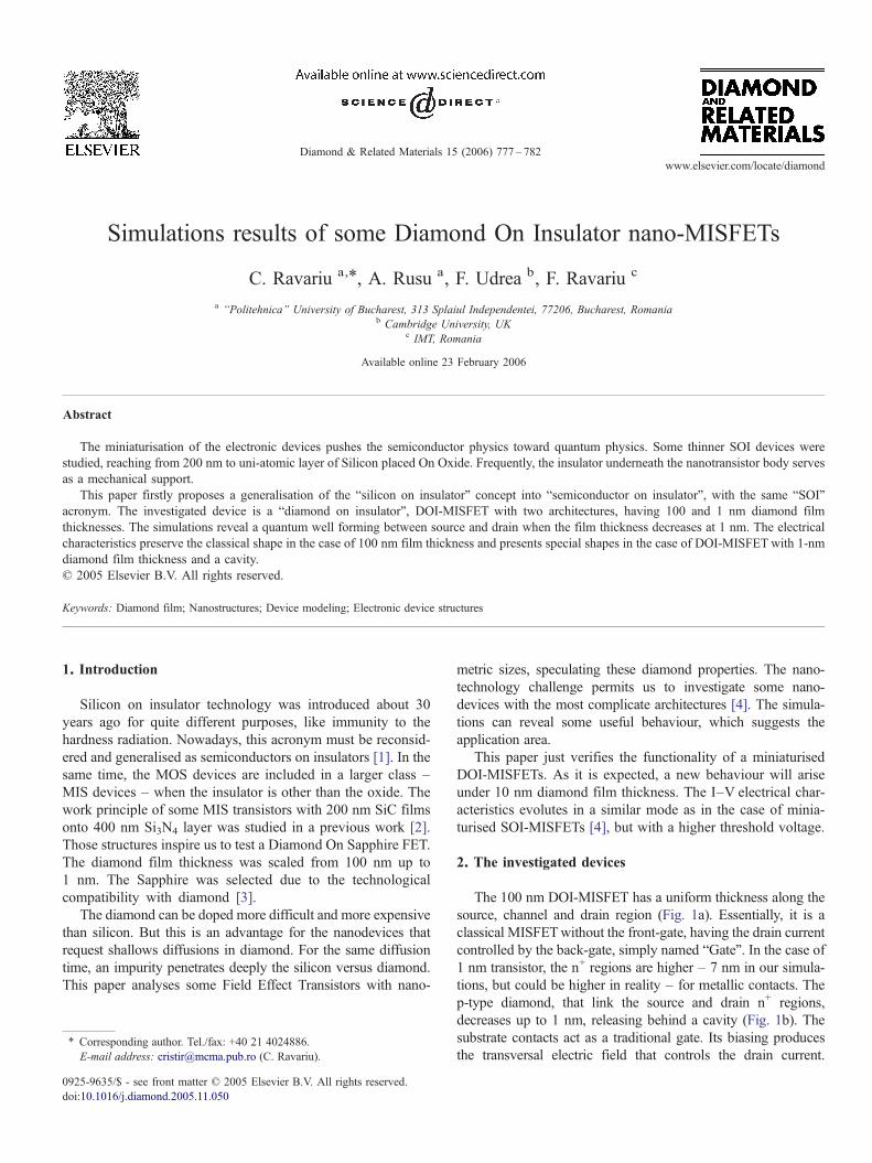
The 100 nm DOI-MISFET has a uniform thickness along thesource, channel and drain region (Fig. 1a). Essentially, it is aclassical MISFETwithout the front-gate, having the drain currentcontrolled by the back-gate, simply named “Gate”. In the case of1 nm transistor, the n+ regions are higher – 7 nm in our simula-tions, but could be higher in reality – for metallic contacts. Thep-type diamond, that link the source and drain n+ regions,decreases up to 1 nm, releasing behind a cavity (Fig. 1b). Thesubstrate contacts act as a traditional gate. Its biasing producesthe transversal electric field that controls the drain current.
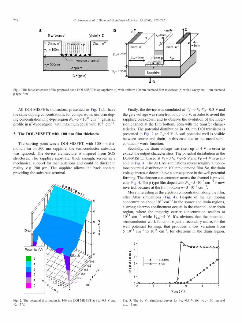
Fig. 1. The basic structures of the proposed nano-DOI-MISFETs on sapphire: (a) with uniform 100 nm diamond film thickness; (b) with a cavity and 1 nm diamondp-type film.
778 C. Ravariu et al. / Diamond & Related Materials 15 (2006) 777–782
All DOI-MISFETs transistors, presented in Fig. 1a,b, havethe same doping concentrations, for comparisons: uniform dop-ing concentration in p-type region NA=5×10
15 cm−3, gaussianprofile in n+-type region, with maximum equal with 1017 cm−3.
3. The DOI-MISFET with 100 nm film thickness
The starting point was a DOI-MISFET, with 100 nm dia-mond film on 500 nm sapphire; the semiconductor substratewas ignored. The device architecture is inspired from SOSstructures. The sapphire substrate, thick enough, serves as amechanical support for manipulations and could be thicker inreality, e.g. 200 μm. The sapphire allows the back contact,providing the substrate terminal.
Fig. 2. The potential distribution in 100 nm DOI-MISFET at VD=0.3 V andVG=5 V.
Firstly, the device was simulated at VS=0 V, VD=0.3 V andthe gate voltage was risen from 0 up to 5 V, in order to avoid thesapphire breakdown and to observe the evolution of the inver-sion channel at the film bottom, both with the transfer charac-teristics. The potential distribution in 100 nm DOI transistor ispresented in Fig. 2 at VG=5 V. A soft potential well is visiblebetween source and drain, in this case due to the metal-semi-conductor work function.
Secondly, the drain voltage was risen up to 4 V in order toextract the output characteristics. The potential distribution in theDOI-MISFET biased at VS=0 V, VG=5 V and VD=4 V is avail-able in Fig. 4. The ATLAS simulations reveal roughly a mono-tone potential distribution in 100 nm diamond film. So, the drainvoltage increase doesn't have a consequence in the well potentialforming. The electron concentration across the channel is provid-ed in Fig. 4. The p-type film doped withNA=5·10
15 cm−3 is nowinverted, because at the film bottom n=3·1017 cm−3.
More interesting is the electron concentration along the film,after Atlas simulations (Fig. 4). Despite of the net dopingconcentration about 1017 cm−3 in the source and drain regions,a strong electron confinement occurs in the channel, near drainregion, where the majority carrier concentration reaches at1015 cm−3 while VDS=4 V. It's obvious that the potential-semiconductor work function is just a secondary cause, for thewell potential forming, that produces a low variation from5·1014 cm-3 to 1015 cm-3, for electrons in the drain region.
0
1
2
3
4
5
0 1 2 3 4 5
6
V GS ( V )
100nm1nm
I D (
n A
/ n
m )
Fig. 3. The ID–VG simulated curves for VD=0.3 V, for yfilm=100 nm andyfilm=1 nm.
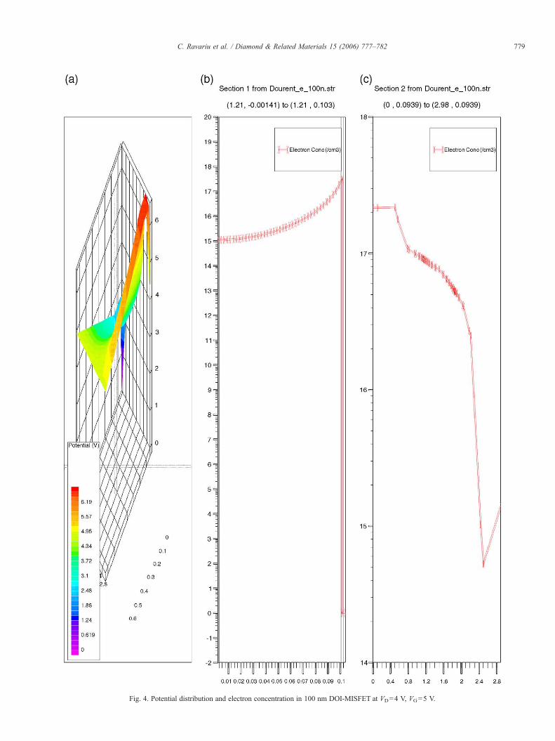
Fig. 4. Potential distribution and electron concentration in 100 nm DOI-MISFET at VD=4 V, VG=5 V.
779C. Ravariu et al. / Diamond & Related Materials 15 (2006) 777–782

0
2
4
6
8
V DS ( V )
0
1
2
3
4
5
6
100nm
1nm
0 1 2 3 4
I D (
n A
/ n
m )
for
100
nm
I D (
n A
/ n
m )
for
1 n
m
10
12
14
16
18
Fig. 6. The ID−VDS simulated curves at VG=−4 V.
780 C. Ravariu et al. / Diamond & Related Materials 15 (2006) 777–782
The main cause is related to the nanometric size of the chan-nel, where the electron concentration decreases with two orderof magnitude, from 2·1017 to 5 ·1014 cm−3 (Fig. 4a,c).
4. The DOI-MISFET with 1 nm p-type diamond onsapphire
A DOI nanotransistor with 1 nm diamond p-type film, withthe same sizes as in Fig. 1b was studied. In fact, the draincurrent is a superposition between the inversion channel currentand tunnel current provided by the electrons from the n+ regionthat tunnel the vacuum cavity, with length xcb4 nm. The cavityvolume is:
Vc ¼ xcd ðynþ−yfilmÞd z ¼ 54 nm3; ð1Þwhere xc is the channel length, yn+ is the n
+ thickness and yfilmthe p-type film thickness. Hence, the air molecules number N,in the cavity is:
N ¼ Vcd NA
Vm0¼ 1; 4 molecules ð2Þ
Consequently, the electron flow isn't disturbed by the airfrom cavity, in normal conditions (Avogadro's numberNA=6023×10
23 molec/mol and normal gass volume per molis Vm0=2242 dm
3/mol). So, the device doesn't require a specialvacuum technology. The simulated 1 nm DOI-MISFET tran-sistor has the same doping concentrations with the 100 nmtransistor: uniform doping concentration in p-type regionNA=5×10
15 cm−3, gaussian profile in n+-type region, withmaximum equal with 1017 cm−3. The ATLAS simulations
Fig. 5. The potential distribution in 1 nm DOI-FET at VG=−4 Vand VD=−1 V.
reveal a quantum well potential in this case, of 1 nm DOI-MISFET, biased at VS=−1 V, VD=0 V, VG=−4V (Fig. 5).
The “nano-effects” were simulated using ATLAS, takinginto account the: Band to Band Tunnelling, Fowler-Nordheimtunnelling, Fermi distribution, Schrodinger's equation, includ-ing in the MODEL statement the following parameters: BBT,FNORD, FERMI, SCHRO [5]. Increasing the gate voltage, thetransfer characteristics were drawn (Fig. 3). Now is the momentto comment them. If the 100 nm DOI-MISFET still preserve aclassical shape of ID–VGS curve, the 1 nm DOI-MISFET pro-duces a new shape, with a maximum. The explanation must berelated to the appearance of the tunnel current through thecavity.
From the characteristics presented in Fig. 3 results the thresh-old voltage, VT=2.8 V for 100 nm device, higher versus asimilar device with SOI structure [4] and 2.2 V for 1 nm device.The criterion for the threshold voltage extraction was adaptedfrom microdevices [6]: voltage that produces 0.1 nA/ nm, whenthe maximum current reaches 1–10 nA/ nm. The transconduc-tance of the characteristic is expressed by the first order deriv-ative. In the threshold vicinity gm=dID /dVG=0.5 nA/V for100 nm device and 10 nA/V for 1 nm device. The nanotran-sistor with 1 nm film thickness presents a steeper character-istic, more suitable for the logic circuits. This device has twostable states for a large range of the gate voltage: (0, 2)V and(2.3, 5)V. For amplifiers or analog circuits, the nano-DOIFETsmust be operated in a sharp domains, where gm is higher (e.g.2.10 VbVGb2.29 V).
The static characteristics, ID–VDS at VGS=−4 V are pre-sented in Fig. 6. In the left side could be read the current for100 nm DOI-MISFET and in the right side the current for 1 nmDOI-MISFETwith cavity. For the first devices (without cavity),the drain current consists of the inversion channel current at thefilm bottom. However, the 100 nm transistor does not have acompletely classical output characteristic. Unusually, there is a“threshold” for the drain voltage, too, VDT=0.2 V. Just over thisvalue the current flows through the transistor, like in a MOS-FET. Then the curve tends to saturate as in the classical case.For the last device with 1 nm film thickness, the drain current iscompletely atypically. The assumption that for the 1 nm devicethe total current is a superposition between the inversion chan-nel current through diamond p-film and the tunnel current
781C. Ravariu et al. / Diamond & Related Materials 15 (2006) 777–782
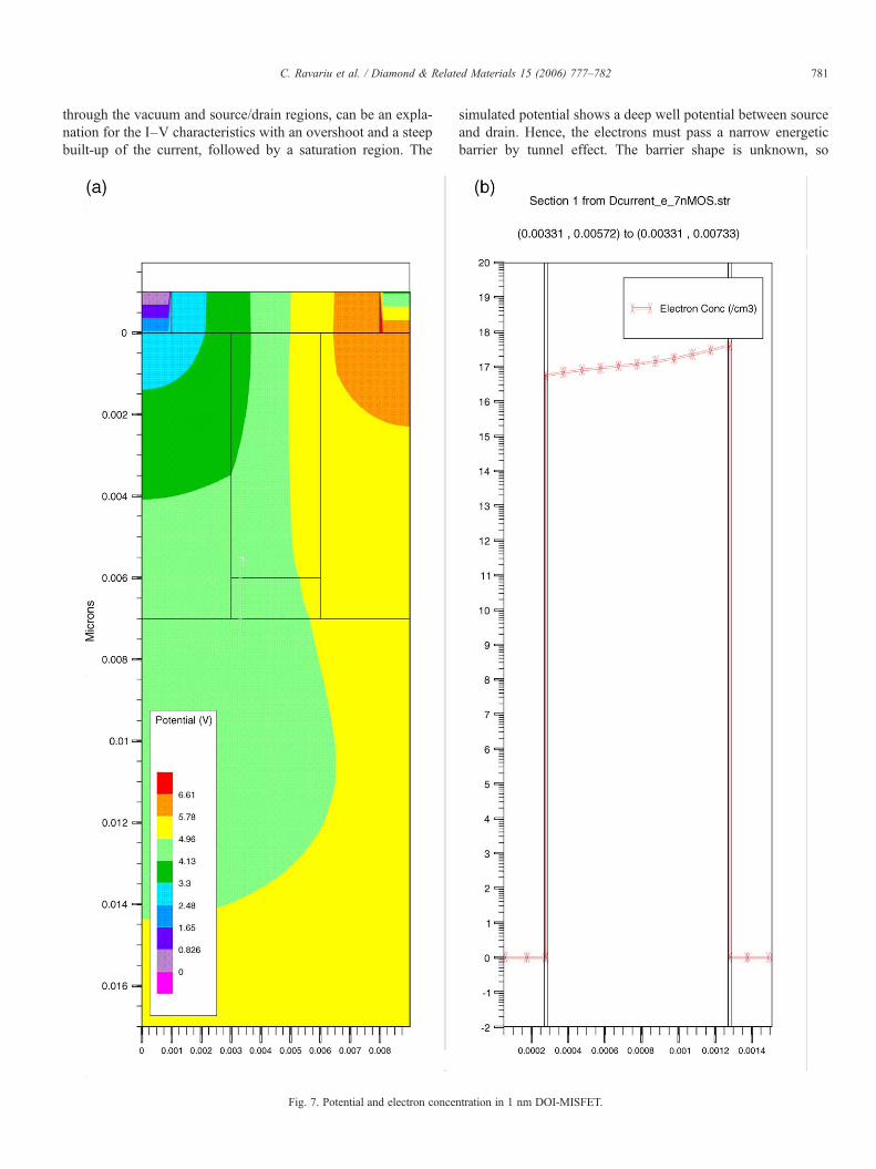
through the vacuum and source/drain regions, can be an expla-nation for the I–V characteristics with an overshoot and a steepbuilt-up of the current, followed by a saturation region. The
Fig. 7. Potential and electron conce
simulated potential shows a deep well potential between sourceand drain. Hence, the electrons must pass a narrow energeticbarrier by tunnel effect. The barrier shape is unknown, so
ntration in 1 nm DOI-MISFET.
782 C. Ravariu et al. / Diamond & Related Materials 15 (2006) 777–782
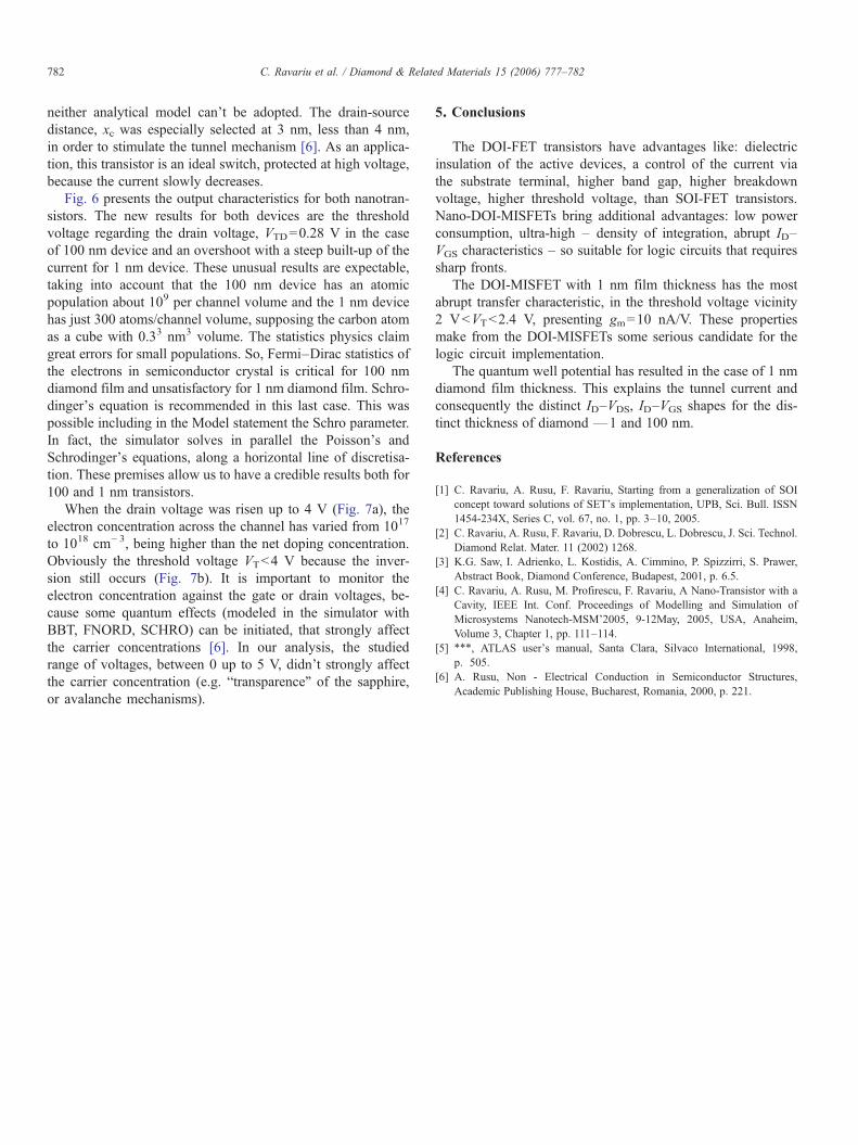
neither analytical model can't be adopted. The drain-sourcedistance, xc was especially selected at 3 nm, less than 4 nm,in order to stimulate the tunnel mechanism [6]. As an applica-tion, this transistor is an ideal switch, protected at high voltage,because the current slowly decreases.
Fig. 6 presents the output characteristics for both nanotran-sistors. The new results for both devices are the thresholdvoltage regarding the drain voltage, VTD=0.28 V in the caseof 100 nm device and an overshoot with a steep built-up of thecurrent for 1 nm device. These unusual results are expectable,taking into account that the 100 nm device has an atomicpopulation about 109 per channel volume and the 1 nm devicehas just 300 atoms/channel volume, supposing the carbon atomas a cube with 0.33 nm3 volume. The statistics physics claimgreat errors for small populations. So, Fermi–Dirac statistics ofthe electrons in semiconductor crystal is critical for 100 nmdiamond film and unsatisfactory for 1 nm diamond film. Schro-dinger's equation is recommended in this last case. This waspossible including in the Model statement the Schro parameter.In fact, the simulator solves in parallel the Poisson's andSchrodinger's equations, along a horizontal line of discretisa-tion. These premises allow us to have a credible results both for100 and 1 nm transistors.
When the drain voltage was risen up to 4 V (Fig. 7a), theelectron concentration across the channel has varied from 1017
to 1018 cm− 3, being higher than the net doping concentration.Obviously the threshold voltage VTb4 V because the inver-sion still occurs (Fig. 7b). It is important to monitor theelectron concentration against the gate or drain voltages, be-cause some quantum effects (modeled in the simulator withBBT, FNORD, SCHRO) can be initiated, that strongly affectthe carrier concentrations [6]. In our analysis, the studiedrange of voltages, between 0 up to 5 V, didn't strongly affectthe carrier concentration (e.g. “transparence” of the sapphire,or avalanche mechanisms).
5. Conclusions
The DOI-FET transistors have advantages like: dielectricinsulation of the active devices, a control of the current viathe substrate terminal, higher band gap, higher breakdownvoltage, higher threshold voltage, than SOI-FET transistors.Nano-DOI-MISFETs bring additional advantages: low powerconsumption, ultra-high – density of integration, abrupt ID–VGS characteristics – so suitable for logic circuits that requiressharp fronts.
The DOI-MISFET with 1 nm film thickness has the mostabrupt transfer characteristic, in the threshold voltage vicinity2 VbVTb2.4 V, presenting gm=10 nA/V. These propertiesmake from the DOI-MISFETs some serious candidate for thelogic circuit implementation.
The quantum well potential has resulted in the case of 1 nmdiamond film thickness. This explains the tunnel current andconsequently the distinct ID–VDS, ID–VGS shapes for the dis-tinct thickness of diamond —1 and 100 nm.
References
[1] C. Ravariu, A. Rusu, F. Ravariu, Starting from a generalization of SOIconcept toward solutions of SET's implementation, UPB, Sci. Bull. ISSN1454-234X, Series C, vol. 67, no. 1, pp. 3–10, 2005.
[2] C. Ravariu, A. Rusu, F. Ravariu, D. Dobrescu, L. Dobrescu, J. Sci. Technol.Diamond Relat. Mater. 11 (2002) 1268.
[3] K.G. Saw, I. Adrienko, L. Kostidis, A. Cimmino, P. Spizzirri, S. Prawer,Abstract Book, Diamond Conference, Budapest, 2001, p. 6.5.
[4] C. Ravariu, A. Rusu, M. Profirescu, F. Ravariu, A Nano-Transistor with aCavity, IEEE Int. Conf. Proceedings of Modelling and Simulation ofMicrosystems Nanotech-MSM'2005, 9-12May, 2005, USA, Anaheim,Volume 3, Chapter 1, pp. 111–114.
[5] ⁎⁎⁎, ATLAS user's manual, Santa Clara, Silvaco International, 1998,p. 505.
[6] A. Rusu, Non - Electrical Conduction in Semiconductor Structures,Academic Publishing House, Bucharest, Romania, 2000, p. 221.