silicon photonics for mid-board optical modules · conclusion •the combination of mid-board...
TRANSCRIPT

Marc Epitaux
Silicon Photonics for Mid-Board Optical Modules
Chief Architect at Samtec, Inc

Outline
• Interconnect Solutions
• Mid-Board Optical Modules
• Silicon Photonics
o Benefits
o Challenges
• DragonFly Packaging Platform
• Conclusion

Interconnect Challenges
• Raw speed
• Distance
• Size
• Cooling and thermals
• Various environmental constraints
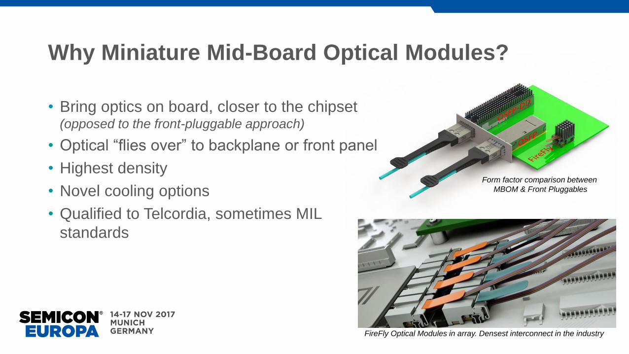
Why Miniature Mid-Board Optical Modules?
• Bring optics on board, closer to the chipset (opposed to the front-pluggable approach)
• Optical “flies over” to backplane or front panel
• Highest density
• Novel cooling options
• Qualified to Telcordia, sometimes MIL
standards
Form factor comparison between
MBOM & Front Pluggables
FireFly Optical Modules in array. Densest interconnect in the industry

Mid-Board Optics Standardization
Consortium for On-Board Optics
• Effort to standardize on-board optics
• Has adopted a two connectors mounting concept
• Two lane width proposed: 8x and 16x
• Three module length proposed
• 0.6mm pitch highspeed connector
• Full specification expected by mid-year with first
sample Q1’18

Why Silicon Photonics?
• Direct modulated laser diode is challenged with next
generation data rates (>28Gbps)
• Optical function integration: photodetection, WDM filter,
modulation, splitter
• Higher channel counts (8x, 16x)
• Enable advanced modulation: PAM, WDM, QAM,
DPSK
• Single mode operation allows longer reach (up to 2km)
• Volume manufacturing (wafer processing)

Silicon Photonics Challenges
• Circuit integration
o Platform and CAD tool homogenization
o Limited generic component offering
o Test infrastructure
• Light coupling
o Laser integration
o Single mode fiber coupling and alignment
• Packaging integration
o High speed signaling and interconnect
o Thermal management
Courtesy UCSB
Example: Laser integration
• Platform/PDK?
• Fabrication/foundry?
• Coupling approach?
• Test and Reliability?

DragonFly Packaging Platform
Architectural Features
• MBOM packaging
• Semiconductor manufacturing
• SiPho Engine (BGA’ed)
• Single mode optics
• Flip-chipped PMDs
• Backside illumination
• 4x 56G bandwidth
Development carried out in the IRT Nanoelec program

DragonFly Optical Layout
Optical Features
• Single mode fiber
• Free space optical layout
• Grating Coupler
o 1D output (3dB IL)
o 2D input (6dB IL)
o Mode converter
• Alignment Strategy
o Passive
o Active
0%
10%
20%
30%
40%
50%
60%
70%
80%
90%
100%
0% 10% 20% 30% 40% 50% 60% 70% 80% 90% 100%
FIB
ER C
OU
PLI
NG
EFF
ICIE
NC
Y (%
)
% OF POPULATION
FIBER COUPLING EFFICIENCY FROM 10K MONTE CARLO
Design A Design B Design C Design D Design E
With same tolerances Design D would be better for Active Alignment
Design C: better for Passive Alignment

DragonFly Electrical Signal Integrity
Features
• Organic substrate
• 0.5mm edge connector
• BGA interconnect SiPho chip (200um)
Modeling & Simulation
• Modeled the system in HFSS
• IL: -1.55 dB Insertion loss @ 28 GHz
• RL: < -18 dB up to 28 GHz Nyquist.

DragonFly Thermal Management
200G DragonFly Est. Power
Driver + CDR 1’300mW
TIA + CDR 1’400mW
Laser Driver 400mW
Phase Shifter 100mW
Micro-Controller + IO Ctrl 150mW
Total 3’350mW
Autodesk CFD 360 Simulation
Power Density
• Multi-Gbps interconnect requires signal processing
and electronic compensation (CDR, CTLE, FFE,
DFE, PAM4,…)
• Smaller, integrated device increases drastically the
power density (1.7W/cm2 at the MBOM level)
Heatsink Alternatives
• Convection cooling (not sufficient)
• Conduction cooling
• Immersion

MBOM Implementation Example
Conclusion
• The combination of Mid-Board Optics packaging platform and Silicon Photonics is offering new high performance horizon for optical interconnect:
o Bring the fibers closer to the signal processor (ASIC, FPGA, switch)
o Increase the interconnect density
o Offer a path to 100Gbps and much beyond
o Extend optical link reach
• However the promises of photonics integration is still facing challenges:
o Circuit integration
o Light coupling
o Packaging integration
o A novel Mid-Board Silicon Photonics packaging platform has been presented which address most of those challenges

Thank you
Acknowledgments:• Samtec Team• IRT Nanoelec Partners