silicon-germanium films deposited by low-frequency … films deposited by low-frequency...
TRANSCRIPT

Silicon-germanium films deposited by low-frequencyplasma-enhanced chemical vapor deposition: Effect of H2 andAr dilution
A. Kosarev,a) A. Torres, Y. Hernandez, R. Ambrosio, and C. ZunigaInstitute National for Astrophysics, Optics and Electronics, INAOE, CP 7200, Puebla, Mexico
T.E. FelterLawrence Livermore National Laboratory, Livermore, California 94550
R. Asomoza and Y. KudriavtsevCentro de Investigacion y de Estudios Avanzado del Instituto Politecnico Nacional,Mexico, D.F. 07360
R. Silva-GonzalezInstituto de Fisica, Benemerita Universidad Autonoma de Puebla, Puebla, Pue., C.P. 72570, Mexico
E. Gomez-BarojasCIDS-IC, Benemerita Universidad Autonoma de Puebla, Puebla, Pue. C.P. 72000, Mexico
A. IlinskiBenemerita Universidad Autonoma de Puebla, Puebla, Puebla 72050, Mexico
A.S. AbramovA.F. Ioffe Phys.-Technical Institute, St.-Petersburg 194021, Russia
(Received 21 December 2004; accepted 6 July 2005)
We have studied structure and electrical properties of Si1−YGeY:H films deposited bylow-frequency plasma-enhanced chemical vapor deposition over the entire compositionrange from Y � 0 to Y � 1. The deposition rate of the films and their structural andelectrical properties were measured for various ratios of the germane/silane feed gasesand with and without dilution by Ar and by H2. Structure and composition was studiedby Auger electron spectroscopy (AES), secondary ion mass spectroscopy (SIMS), andFourier transform infrared (FTIR) spectroscopy. Surface morphology was characterizedby atomic force microscopy (AFM). We found that the deposition rate increased withY, maximizing at Y � 1 without dilution. The relative rate of Ge and Si incorporationis affected by dilution. Hydrogen preferentially bonds to silicon. Hydrogen contentdecreases for increasing Y. In addition, optical measurements showed that as Y goesfor 0 to 1, the Fermi level moves from mid gap to the conduction band edge; i.e., thefilms become more n-type. No correlation was found between the pre-exponential andthe activation energy of conductivity. The behavior of the conductivity �-factorsuggests a local minimum in the density of states at E ≈ 0.33 eV for the films grownwith or without H-dilution and E ≈ 0.25 eV for the films with Ar dilution.
I. INTRODUCTION
Silicon-germanium alloys (Si1−YGeY:H) are used as alow-bandgap material in multi-junction amorphous sili-con solar cells1–3 and are of much interest for other ap-plications, e.g., un-cooled micro-bolometers3–4 and inun-cooled bolometers.5–7
Jordan et al.8 have very recently studied a nano-crystalline Ge p-i-n structure. Despite implementation in
device structures, Si1−YGeY:H films have been signifi-cantly less studied and their electronic properties arepoorly understood in comparison to those for amorphoussilicon. Reviews of earlier work on Si1−YGeY:H films canbe found in Refs. 9 and 10. Although radio frequency (rf;f � 13.56 MHz) plasma-enhanced chemical vapor depo-sition (PECVD) remains the major technique for fabri-cation of Si1−YGeY:H films, alternative methods, such as,electron-cyclotron resonance (ECR) plasma deposition11
and non-plasma hot wire (HW) deposition,12 have alsodemonstrated promising results. Dalal et al.13 have founda positive role of ion bombardment on film growth and
a)Address all correspondence to this author.e-mail: [email protected]
DOI: 10.1557/JMR.2006.0013
J. Mater. Res., Vol. 21, No. 1, Jan 2006 © 2006 Materials Research Society88

electronic properties of Si1−YGeY:H films. With this inmind, a low-frequency (LF) capacitive discharge, whichhas thicker near electrode sheathes,14 could provide in-creased ion bombardment. Nevertheless, only one paper,Budagian et al.15 reports LF PECVD deposition ofSi1−YGeY:H films. Although the various investigationshave found that the optoelectronic properties of thesefilms change significantly with deposition conditions, itseems that all these methods of alloying Si with Ge resultin deterioration of the photo-electronic properties. Mostof the publications deal with relatively low Ge concen-tration (Y < 0.5) and only these films have providedopto-electronic properties suitable for application in de-vice structures. The investigation of Si1−YGeY:H filmsover the entire range 0 � Y � 1 has been reported inRefs. 16–18. Feed gases (SiH4, GeH4 or GeF4) have beenmixed with the dilution gas Ar,19 He,17 or H2.20 Thelatter is of great importance for fabrication of micro-21
and nano-crystalline films.22,23 Nevertheless, the effectof dilution gas on both film growth and electronic prop-erties has not been systematically studied.
The present report concerns an investigation ofgrowth, structural, optical, and electrical properties ofSi1−YGeY:H films over the entire range of Ge concentra-tions 0 � Y � 1 in films deposited by LF PECVD fromsilane-germane mixtures with and without argon and hy-drogen gas dilution.
II. EXPERIMENT
The samples of amorphous silicon germanium filmswere prepared by LF PECVD decomposition using amodernized PECVD system from Applied Materials Inc.(Santa Clara, CA), Model 3300. Silane, SiH4, and ger-mane, GeH4, were used as the feed gases and hydrogenand argon as the dilution gases. Two different substrateswere used: Corning (Danville, VA) 1737 glass for theconductivity measurements and crystalline silicon (c-Si)for the measurements of infrared spectra. The films weredeposited at substrate temperature Ts � 300 °C. Thedeposition parameters were as follows: pressure, P �0.6 Torr; power, W � 350 W; and frequency f �110 kHz. The total flow of silane and germaniumQSiH4,GeH4 was 50 sccm for all depositions. Three typesof the samples were fabricated: 20:1 hydrogen dilution(H-dilution), 10:1 argon dilution (Ar-dilution), and undi-luted. Prior to film growth on glass substrates, stripes ofaluminum electrodes with 1–2 mm inter-electrode dis-tance were deposited by e-beam evaporation. For puregermanium samples, i.e., Y � 1, a silicon nitride layerwas deposited after film growth to protect the sample andavoid oxidation. The germane content in the gas phase X,defined as the gas flow ratio X � QGeH4/QSiH4+GeH4, wasvaried from 0 to 1. The thickness of the films was meas-ured by a Dektak II step profiler. Composition of the
films was characterized by secondary ion mass spectros-copy (SIMS) and Auger electron spectroscopy (AES).SIMS profiles were measured with a Cameca (Courbe-voie, France) IMS-6f ion microprobe. Sputtering duringSIMS utilized a cesium ion beam with primary ion en-ergy from 5 to 15 keV. The primary ion beam was rasterscanned at approximately 200 �m, and the secondaryions emitted from a central area of 60 �m were moni-tored after mass and energy separation with an electronmultiplier.
We monitored negative secondary ions to check con-taminants H, C, O, and N. The solid solution compositionwas analyzed with a special mode in which secondaryions CsM+ (where M is the analyzed element) weremonitored during cesium sputtering. Oxygen floodingwas always used with this mode to minimize the SIMSmatrix effect found in SiGe compounds. We deposited athin gold film on the surface of samples prone to charg-ing and applied an electron beam charge compensationtechnique during the SIMS analysis.
The AES data were obtained by means of a JEOL(JEOL Ltd., Tokyo, Japan) system, Model JAMP-7800,with hemispherical electrostatic Auger energy analyzer.The system operates in ultrahigh vacuum (�10−8 Pa)with energy resolution of 0.6% to 0.06%. The Augerspectra were recorded using a 10 keV electron beam at 5× 10⁻⁸ A after the samples were sputtered clean by anAr+ ion beam with kinetic energy of 3 keV and rasteredover a 20 × 35 �m area. The Si(LVV), N(KLL),Ge(LMM), and Si(KLL) transitions were observed in theAuger spectra. The Si(KLL) line was used for semi-quantified analysis of the concentration as discussed inSec. III. B.
Atomic force microscopy (AFM) was used to studysurface morphology of the films. These measurementswere conducted with a Quesant (Agoura Hills, CA) Scan-ning Probe Microscope. Hydrogen bonding in the filmswas studied by Fourier transform infrared (FTIR) spec-troscopy. The infrared (IR) absorption spectra of thefilms were measured with a Brucker (Brucker Optics,Ettingen, Germany) infrared spectrometer, Model Vec-tor-22 over the range 350–4000 cm−1. The measuredtransmission spectra were normalized to the transmissionspectrum of a crystalline silicon substrate, and the absorp-tion coefficient was determined by the Brodsky–Cardona–Cuomo method.24
The spectral dependence of the optical absorption co-efficient �(h�) was calculated from optical transmissionT(h�) measurements by the method described in Refs.25, 26. T(h�) was measured with a Perkin Elmer (PerkinElmer Inc., Wellesley, MA) spectrophotometer ModelLambda 3B. Optical constants, namely the refractive in-dex n and the extinction coefficient k, were determined at� � 0.63 �m by variable angle ellipsometry (VAR) us-ing a EL X-02 C (ElipsometerBau GmbH, Ratzeburg,
A. Kosarev et al.: Silicon-germanium films deposited by low-frequency plasma-enhanced chemical vapor deposition: Effect of H2 and Ar dilution
J. Mater. Res., Vol. 21, No. 1, Jan 2006 89

Germany) ellipsometer. The conductivity of the filmswas measured in the direct current (dc) regime in avacuum thermostat with bias voltage Ub � 40 V. Thetemperature dependence of conductivity was measuredwith the heating-cooling rate of approximately 1°/min.
III. RESULTS
A. Film growth
Depending on gas dilutor, we observed different depo-sition rates of the films for X ranging from 0 (pure Si) to1 (pure Ge). The deposition rate was measured by divid-ing the film thickness by deposition time. Figure 1 showsthe dependence of deposition rate Vd on germanium con-tent in the film for the three cases, hydrogen dilution,argon dilution and without dilution. At low Ge-contentX � 0.1, the highest rate Vd � 2.5 A/s was observed inthe films deposited with Ar dilution, and the lowest rateVd � 1.5 A/s in the films deposited with H-dilution. Inall cases, Vd increases with Ge content but the detailedform of Vd � f(X) depends on gas-dilutor. In samplesfabricated without dilution, Vd increased with X andreached the maximum rate of 3.7 A/s at X � 1. WithH-dilution, Vd initially increased rapidly, then moreslowly to a maximum of 2.8 A/s again at X � 1. WithAr dilution, Vd first decreases, reaching a minimum atX � 0.2, and then slowly increases to 3 A/s at X � 1.The growth of these Si1−YGeY:H films will be discussedin Section 4 and compared with the literature.
B. Composition characterization
SIMS profiling and Auger spectroscopy (AES) wereused to characterize the composition of the films. SIMSprofiles are shown in Fig. 2 for representative samplesdeposited with hydrogen dilution. In our analysis, we use
only the values of the concentrations determined in themiddle part of the film excluding interface regions. Theabsolute values of Si and Ge concentrations wereobtained assuming the concentration of Si atoms isNSi � 5 × 10²² atoms/cm3 in the pure Si substrateand the concentration of Ge atoms is NGe � 4.4 ×10²² atoms/cm3 in the pure Ge films. The “peaking” of Siand Ge at the interfaces is caused by the SIMS matrixeffect. We analyzed the film composition in the CsM+
mode with oxygen flooding. The result obtained wascompared with the AES measurements and with SIMSmeasurements of negative Si and Ge ions using relativesensitivity factors (RSF) for a Si matrix. We analyzed C,H, and O as negative atomic ions, whereas nitrogen wasanalyzed as SiN− and GeN− molecular ions. The concen-tration of these elements (C, H, N, and O) was estimatedwith RSFs obtained for implanted Si standards. The in-corporation of Ge, Si, H, and O atoms was studied in thefilms prepared with different germanium feed gas con-tents (X) and with different dilutions. The efficiency ofGe incorporation is of great importance and seldom re-ported in the literature. Figure 3 shows the Ge-content inour films defined as Y � NGe/(NGe + NSi) as a functionof Ge content in the feed gas X. The experimental pointsobtained by both SIMS (filled symbols) and AES (cor-responding unfilled symbols) are presented. They are inagreement within 10%. Some of the discrepancy is re-lated to different probe depths; AES is more sensitive tothe surface (subsurface) region than the SIMS signal ob-tained from a region near mid-thickness. The incorpora-tion of hydrogen and oxygen in our films will be dis-cussed together with infrared (IR) data in Sec. III. D.
C. AFM characterization
Surface morphology of the films was characterized byAFM. AFM images (with dimensions 2 × 2 �m) weretaken for randomly selected parts of the sample. Statis-tical analysis of the surface roughness of the images wasperformed for the AFM images described by the functionof height distribution Z (x, y). Height histograms wereplotted and the following characteristics were deter-mined: average height ⟨Z⟩, average roughness Ra, stan-dard deviation of Z-height (root mean square, rms) Rq,and correlation length Lc. Determination of these char-acteristics are described, e.g., in Ref. 27. These charac-teristics are listed in Table I. We can see from Table Ithat roughness, measured as Rq and Ra, changed with Gecontent, X, Y, and these changes depend on the dilutionused. In the films deposited with H-dilution, roughnessRa (Rq) increases from 0.6(0.8) to 3.1(4.0) nm as Y in-creases from 0.42 to 0.0.87. In the films deposited withAr dilution, no significant change was observed as Y goesfrom 0.23 to 0.90. In the films obtained without dilution,roughness Ra (Rq) increases from 0.6(0.8) to 13(15) nmwith Y for Y � 0.33 to 0.79. Correlation length showed
FIG. 1. Deposition rate as a function of X, the germanium content inthe feed gas, defined as the gas flow ratio X � QGeH4/QSiH4+GeH4.
A. Kosarev et al.: Silicon-germanium films deposited by low-frequency plasma-enhanced chemical vapor deposition: Effect of H2 and Ar dilution
J. Mater. Res., Vol. 21, No. 1, Jan 200690

more complex behavior with Y: growth of Lc from 42(Y � 0.33) to 149 nm (Y � 0.79) in the films depositedwithout dilution, minimum Lc � 40 nm at Y � 0.60 inthe films deposited with Ar dilution, and maximum Lc �95 nm at Y � 0.62 in the films obtained with hydrogendilution.
D. IR spectra
General views of IR spectra for the Si1–YGeY:Hsamples are shown in Fig. 4(a) for X � 0, 0.1 andFig. 4(b) for X � 1. The spectra contain lines corre-sponding to stretching modes at approximately 2000 cm−1
for Si–H and 1880 cm−1 for Ge–H bonds. The rockingand wagging deformation modes are seen at approxi-mately 640 cm−1 for Si–H and 560 cm−1 for Ge–H. Themode at 1950–2000 cm−1 can also be related to the ab-sorption of the stretching mode of Ge–H and to Ge–H2
bonds located on surfaces, e.g., on surfaces of voids as
FIG. 2. SIMS profiles for Si1−YGeY:H films deposited with H-dilutionand various values of the germanium content in the feed gas, X �(a) 0.1, (b) 0.5, and (c) 1.
FIG. 3. (a) Germanium (Ge) content in film Y versus germanium(GeH4) content in feed gas X, and (b) an example of Y(X) best fit toEq. (12) with PGe as variable parameter for the films deposited withH-dilution.
A. Kosarev et al.: Silicon-germanium films deposited by low-frequency plasma-enhanced chemical vapor deposition: Effect of H2 and Ar dilution
J. Mater. Res., Vol. 21, No. 1, Jan 2006 91

reported by Comedi et al.28 In this case, however, thisline should exist in a-Ge:H films, which has not beenobserved in the films studied, see Fig. 4(b). Therefore,we assign the absorption at 2000 cm−1 to Si–H bondingbecause it was observed only in films that containedSi atoms.
The absorption related to Si–O and Ge–O bonds wasobserved in the range of 990–1100 cm−1 and 690–840 cm−1 respectively. Lukovsky et al.29 have assignedabsorption at 860–870 cm−1 to the Ge–O–Ge stretchingmode resulting from oxygen incorporation during plasmagrowth. The vibrational mode at 960 cm−1 was observedin almost all Si–Ge films, but it could not be unambigu-ously assigned. This line has been observed in previousIR spectra but was not assigned.30 It has been reportedearlier by Lukovsky et al.31,32 that absorption bands at650 and 940 cm−1 appeared in oxygen-doped a-Si:Hfilms. The position of the lines k0, their widths w, andareas S, obtained after analyzing the spectra are listed inTable II.
The concentration of chemical bonds, e.g., Si–H, canbe determined from the area of the corresponding lineeither for stretching or for deformation mode by means ofthe equation
NSi−H = A �−�
+���k�
kdk ≈
A
kO× S �cm−3� , (1)
where A is a constant determined from other experiments(e.g., hydrogen effusion33,34 nuclear-reaction analysis,35
nuclear magnetic resonance36 etc.), �(k) is the spectraldependence of the IR absorption in the vicinity of the lineat k � k0, and S is the area under the corresponding line.
Then, assuming that all hydrogen is chemicallybonded, e.g., with Si in a-Si–H films, it is possible tocalculate the hydrogen concentration
CH =NSi−H
× 100 �at.%� , (2)
where is atomic density in atoms/cm3.There is little data in the literature regarding the A-
values for stretching and deformation modes in Si–Hbonds25,33,37–39 and even less in Ge–H bonds.33,37,38 Itshould also be noted that A-values for films deposited by
TABLE I. Surface morphology parameters obtained from AFM measurements.
Sampleno. X Y Dilution
Morphology parameters
Avg. height,⟨Z⟩
(nm)Ra
(nm)
rmsRq
(nm)
Correlationlength Lc
(nm)
170 0 0 H2 5.1 0.79 1.0 60171 0.1 0.42 H2 7.6 0.6 0.8 17173 0.1 0.23 Argon 6.3 1.7 2.3 72175 0.1 0.33 None 3.1 0.6 0.8 42181 0.2 0.62 H2 9.4 1.6 2.1 95183 0.2 0.60 Argon 6.7 1.6 2.0 40186 0.2 0.45 None 8.5 2.1 3.0 58188 0.5 0.87 H2 12.3 3.1 4.0 55190 0.5 0.90 Argon 9.0 1.3 1.8 85192 0.5 0.79 None 35 13 15 149
FIG. 4. General view of IR spectra of the Si1−YGeY:H samples depos-ited with different dilutions and (a) X � 0.1 and (b) X � 1. The IRspectrum for a-Si:H film (X � 0) is shown for comparison.
A. Kosarev et al.: Silicon-germanium films deposited by low-frequency plasma-enhanced chemical vapor deposition: Effect of H2 and Ar dilution
J. Mater. Res., Vol. 21, No. 1, Jan 200692

TABLE II. FTIR data for the Si1−YGeY:H films.
Sample K (cm−1) W (cm−1) S (cm−2) Bonding
S170a-Si:HX � 0Y � 0
644.5 ± 0.4 78.2 ± 0.7 (8.76 ± 0.07) × 104 SiHn
999 ± 3 104 ± 2 (9.4 ± 0.5) × 104 Si–O in different1051.5 ± 0.7 60 ± 3 (3.2 ± 0.5) × 104 configurations2004.3 ± 0.9 71.8 ± 0.8 (1.38 ± 0.05) × 104 SiH2079.4 ± 0.8 88.5 ± 0.8 (2.73 ± 0.05) × 104 SiH or SiH2
S171X � 0.10Y � 0.42H-dilution
550 ± 20 52 ± 7 (1.7 ± 1.7) × 104 GeHn
592 ± 3 58 ± 10 (7 ± 3) × 104 GeHn
647 ± 5 62 ± 3 (6 ± 1) × 104 SiHn
782.4 ± 0.8 46 ± 1 (6.8 ± 0.3) × 103 GeHn(?), Si–O–Si–Hn(?)872 ± 6 79 ± 7 (1.3 ± 0.4) × 104 Ge–O–Ge966 ± 3 104 ± 7 (5.0 ± 0.4) × 104 GeO, Si–O, (?)
1058 ± 3 43 ± 9 (1.5 ± 0.8) × 103 Si–O1885.4 ± 0.5 66 ± 1 (1.45 ± 0.02) × 104 GeH2025.8 ± 0.3 95.0 ± 0.7 (4.30 ± 0.02) × 104 SiH
S174with Si3N4
X � 0.10Y � 0.23Ar dilution
596 ± 2 71 ± 1 (5.3 ± 0.2) × 104 GeHn
653 ± 2 60 ± 1 (2.8 ± 0.2) × 104 SiHn
798 ± 3 58 ± 4 (6.0 ± 0.8) × 103 GeHn(?), Si–CH3(?)874 ± 2 77 ± 6 (1.4 ± 0.2) × 104 Ge–O–Ge968 ± 2 122 ± 2 (5.2 ± 0.2) × 104 Si–O(?), Ge–O(?)
1883.9 ± 0.8 61 ± 2 (5.0 ± 0.1) × 103 GeH2031.8 ± 0.4 112.7 ± 0.8 (2.79 ± 0.02) × 104 SiH
S175X � 0.10Y � 0.33No dilution
619.9 ± 0.2 104 ± 1 (1.49 ± 0.02) × 105 SiHn
881.3 ± 0.6 32 ± 1 (2.0 ± 0.1) × 103 Ge–O–Ge964.6 ± 0.3 101.0 ± 0.6 (3.44 ± 0.02) × 104 Si–O(?), Ge–O(?)
1883 ± 1 59 ± 2 (6.9 ± 0.2) × 103 GeH2030.2 ± 0.3 109.7 ± 0.8 (4.84 ± 0.03) × 104 SiH
S181X � 0.20Y � 0.62H-dilution
584.7 ± 0.7 78.9 ± 0.8 (7.5 ± 0.1) × 104 GeHn
652 ± 1 54.0 ± 1 (1.7 ± 0.1) × 104 SiHn
875 ± 1 43 ± 4 (2.0 ± 0.4) × 103 Ge–O–Ge953.1 ± 7.21 103.4 ± 7.3 (2.7 ± 0.4) × 104 Si–O(?), Ge–O(?)
1025.4 ± 32.2 89 ± 20 (3 ± 4) × 103 Si–O1881.9 ± 0.2 65.7 ± 0.4 (2.13 ± 0.01) × 104 GeH2016.8 ± 0.3 82.5 ± 0.6 (2.32 ± 0.01) × 104 SiH
S183X � 0.20Y � 0.64Ar dilution
586.6 ± 0.9 75 ± 1 (9.3 ± 0.2) × 104 GeHn
652 ± 1 57 ± 1 (3.2 ± 0.2) × 104 SiH766 ± 1 25 ± 3 (1.1 ± 0.4) × 103 GeHn
801 ± 2 45 ± 7 (3.4 ± 0.7) × 103 GeHn(?), Si–CH3?867 ± 2 60 ± 4 (6.1 ± 0.8) × 103 Ge–O–Ge958 ± 1 129 ± 2 (3.90 ± 0.08) × 104 Si–O(?), Ge–O(?)
1072.9 ± 0.7 28 ± 2 (9 ± 1) × 102 Si–O1884.8 ± 0.3 65.5 ± 0.7 (1.71 ± 0.01) × 104 GeHn
2019.5 ± 0.3 85.8 ± 0.7 (2.67 ± 0.01) × 104 SiHn
S186X � 0.20Y � 0.45No dilution
593 ± 1 73 ± 1 (6.9 ± 0.2) 104 SiH2
655 ± 1 57 ± 1 (3.2 ± 0.2) × 104 Si–H878.9 ± 0.7 38 ± 2 (1.8 ± 0.2) × 103 Ge–O–Ge963.1 ± 0.3 110 ± 1 (3.94 ± 0.03) × 104 Si–O(?), Ge–O(?)
1073 ± 1 25 ± 3 (5.6 ± 0.7) × 102 Si–O1886.0 ± 0.6 64 ± 1 (9.6 ± 0.1) × 103 GeH2025.3 ± 0.3 96.8 ± 0.7 (2.98 ± 0.02) × 104 SiH
S188X � 0.50Y � 0.87H-dilution
564 ± 3 60 ± 3 (3.4 ± 0.8) × 104 GeH620 ± 20 83 ± 14 (2.0 ± 0.8) × 104 Si–H882 ± 4 65 ± 8 (7.3 ± 3.4) × 103 Ge–O–Ge977 ± 2 110 ± 20 (3.2 ± 0.6) × 104 Ge–O(?)
1060 ± 2 49 ± 14 (2.9 ± 2.6) × 103 Si–O1874.1 ± 0.2 62.9 ± 0.3 (2.49 ± 0.01) × 104 GeH1998 ± 1 93 ± 3 (5.6 ± 0.1) × 103 SiH
S190X � 0.50Y � 0.90Ar dilution
560 ± 3 65 ± 3 (5 ± 1) × 104 GeH610 ± 11 82 ± 7 (4 ± 1) × 104 SiH779 ± 1 43 ± 4 (1.7 ± 0.3) × 103 (?)912 ± 9 160 ± 11 (4.4 ± 0.5) × 104 Ge–O(?)
1014 ± 6 106 ± 14 (7.3 ± 4.6) × 103 Si–O1878.4 ± 0.2 59.9 ± 0.3 (2.54 ± 0.01) × 104 GeHn
2010.6 ± 0.7 66 ± 1 (6.9 ± 0.1) × 103 SiHn
(continued)
A. Kosarev et al.: Silicon-germanium films deposited by low-frequency plasma-enhanced chemical vapor deposition: Effect of H2 and Ar dilution
J. Mater. Res., Vol. 21, No. 1, Jan 2006 93

different techniques and by different laboratories canvary. This makes it difficult to calculate H-concentrationusing IR data and A-values from the literature. Never-theless, we have estimated CH using Eqs. (1) and (2) andsubstituting ASi-Hstr (2000) � 9 × 1019 cm−2,39 ASi-Hdef
(630) � 2.1 × 1019 cm−2,39 and AGe–Hstr (1880) � 5 ×1019 cm−2,37 to reveal trends in CH with increasing Gecontent in the film and with dilution in the feed gas.Relative errors in the estimations are determined by theerrors related with calculation of S in Eq. (1), which areless than 1%. This is acceptable for comparative analysis.Errors in absolute values of hydrogen concentration aremainly determined by A constants.
Figure 5 shows H-content CH as a function of Ge-content Y in the films. Generally, CH reduces with in-creasing Y. The minimum value of CH occurs at CH ≈ 1at.% for Ge films (Y � 1) and is achieved in the filmsdeposited without dilution. Films deposited with eitherH- or Ar-dilution had approximately twice the hydrogencontent, CH ≈ 2 at.%. At low Ge content (Y � 0.1), thehighest values of hydrogen content are CH ≈ 5.5 at.% andare observed for films deposited with H-dilution.
It is interesting to compare the behavior of CH deter-mined by both FTIR and SIMS with the Ge content Y inthe film. Both data show a similar general trend: CH
reduces with increasing Ge. FTIR and SIMS data dem-onstrate good agreement in the range of Y � 0.5 to 1.0.For low Ge content, Y � 0.1 to 0.5, the two methodsdisagree by approximately a factor of 2.
In a similar way, using the absorption line in the region850 < k < 1050 cm−1, we estimate the oxygen content CO
in the films by substituting the corresponding A-value:A � 0.156 at.%/eVcm−1.38 Note, we use this value forboth Si–O and Ge–O bonds because, to our knowledge,the A-constant for Ge–O bonds has not been reported.The behavior of CO determined by both FTIR and SIMSversus Y is shown in Fig. 6. All films showed O-contentreducing with Y increasing. The discrepancy, however,between the CO values determined by FTIR and by SIMSwas typically a factor of 2–4. The lowest O-content wasobserved by both techniques at Y � 1, i.e., for pure a-Gefilms. Nelson et al.40 have also reported a decrease of theoxygen concentration as measured by SIMS with Y for
TABLE II. FTIR data for the Si1−YGeY:H films. (continued)
Sample K (cm−1) W (cm−1) S (cm−2) Bonding
S192X � 0.50Y � 0.79No dilution
562 ± 3 66 ± 2 (3.7 ± 0.7) × 104 GeH617 ± 8 81 ± 6 (3.3 ± 0.7) × 104 SiH883 ± 3 71 ± 2 (4.8 ± 0.8) × 103 Ge–O–Ge961 ± 2 95 ± 4 (1.93 ± 0.09) × 104 Ge–O(?)
1045.2 ± 0.7 41 ± 2 (1.2 ± 0.2) × 103 Si–O1875.7 ± 0.1 60.4 ± 0.2 (2.253 ± 0.007) × 104 GeH2013.8 ± 0.3 67.6 ± 0.7 (8.7 ± 0.08) × 103 SiH
S195with Si3N4
X � 1.00Y � 1.00H-dilution
556 ± 3 73 ± 3 (3.9 ± 0.3) × 104 GeH612 ± 4 57 ± 8 (1.1 ± 0.5) × 104 SiH(?)684 ± 7 77 ± 9 (9 ± 2) × 103 SiH(?)897 ± 2 120 ± 3 (1.74 ± 0.04) × 104 Ge–O–Ge986 ± 1 58 ± 3 (4.0 ± 0.4) × 103 Ge–O(?)
1873.5 ± 0.3 46.3 ± 0.6 (1.19 ± 0.01) × 104 GeHS197with Si3N4
X � 1.00Y � 1.00Ar dilution
562 ± 1 75 ± 3 (3.7 ± 0.5) × 104 GeH630 ± 18 120 ± 17 (1.9 ± 0.5) × 104 SiH(?)887 ± 3 106 ± 4 (1.26 ± 0.06) × 104 Ge–O–Ge977 ± 2 78 ± 2 (7.5 ± 0.6) × 103 Si–O(?), Ge–O(?)
1877.1 ± 0.4 51 ± 0.7 (1.58 ± 0.02) × 104 GeHn
S199with Si3N4
X � 1.00Y � 1.00No dilution
557 ± 3 67 ± 2 (2.5 ± 0.3) × 104 GeH609 ± 6 61 ± 4 (10 ± 3) × 103 SiH(?)824 ± 1 73 ± 4 (1.7 ± 0.4) × 104 GeH2,887 ± 12 120 ± 10 (2.0 ± 0.4) × 104 Ge–O–Ge
1875.8 ± 0.4 49.4 ± 0.8 (1.48 ± 0.02) × 104 GeHn
FIG. 5. Dependence of hydrogen content CH in the film on Ge-contentY, determined from both FTIR and SIMS data.
A. Kosarev et al.: Silicon-germanium films deposited by low-frequency plasma-enhanced chemical vapor deposition: Effect of H2 and Ar dilution
J. Mater. Res., Vol. 21, No. 1, Jan 200694

Y > 0.5 without reporting a mechanism or reason for thisbehavior. As known for a-Si:H films, there should besome quantity of hydrogen that optimally terminates dan-gling bonds in the Si1−YGeY:H films and thereforeachieves the best electronic properties. We could alsoexpect some optimal distribution of this hydrogen be-tween the Si and Ge atoms since the sensitivity of elec-tronic properties to dangling bonds need not be the samefor Si and Ge atoms. The problem of hydrogen distribu-tion between Si and Ge atoms in Si–Ge films has beendiscussed in Refs. 41–43, but the optimum concentrationhas not yet been reported in the literature.
To characterize the hydrogen distribution in the filmsstudied we use a parameter called “Ge–H preference”
PGe−H = �SGe−H
SSi−H��� Y
1 − Y� ,
where Y is the Ge content in the film and SGe–H and SSi–H
are the areas of the absorption lines corresponding to thestretching mode of Ge–H and Si–H bonds, respectively.P � 1 corresponds to a proportional distribution of hy-drogen between Si and Ge atoms. P < 1 reflects that Geatoms are under-terminated by hydrogen and there areextra Ge dangling bonds. P > 1 indicates that there areextra Si dangling bonds. PGe–H values calculated fromthe IR data are as follows: PGe–H � 0.45 ± 02, 0.61 ±0.04, and 0.29 ± 0.04, for the films deposited with hy-drogen, argon and without dilution, respectively. Wehave observed only PGe–H < 1. This suggests that hydro-gen is not evenly distributed between the Ge and Si at-oms in Si–Ge films. The distribution, i.e., the exact valueof PGe–H, depends on the dilution gas mixture duringgrowth.
E. Optical absorption measurements
1. Spectral dependence of optical absorption
The spectral dependence of the optical absorption co-efficient �(h�) is shown in Fig. 7(a) for all the samplesstudied along with that for a-Si for comparison. As canbe seen, �(h�) curves shift to lower photon energy withincreasing Ge content in the feed gas. The total shift isabout 0.9 eV when Y changes from 0 to 1. The shift is notproportional to Y; nearly half of the total shift occurs inthe low Y region between Y � 0 and Y � 0.42. Theeffect of dilution is rather pronounced for Y � 0.23 to0.6; the films deposited with H-dilution are shifted morethan the others.
To determine the optical band gap Eg, we follow themethod of Tauc. Thus, the �(h�) curves are re-plotted as
��h� = f�h�� ,FIG. 6. Oxygen content determined by both SIMS and FTIR as afunction of Ge-content in solid phase CO(Y) for Si1−YGeY:H filmsdeposited with different dilutions.
FIG. 7. Spectral dependence of optical absorption coefficient:(a) �(h�) and (b) Tauc plots √�h� = f(h�) of the Si1−YGeY:H filmsdeposited from the gas mixtures with different Ge-content Y and dif-ferent dilutions.
A. Kosarev et al.: Silicon-germanium films deposited by low-frequency plasma-enhanced chemical vapor deposition: Effect of H2 and Ar dilution
J. Mater. Res., Vol. 21, No. 1, Jan 2006 95

[Fig. 7(b)], and the optical parameters are determinedfrom the best fit of the experimental points to the equa-tion:
��h� = B�h� − Eg� . (3)
Additionally, we determine the photon energies E03
and E04 as those providing absorption coefficients � �103 and � � 104 cm−1, respectively. Their difference,E � E04 − E03, characterizes the slope of �(h�). Theoptical characteristics discussed above are listed inTable III. The B-factor can be calculated from the bandtail density of states using the equation B2 � (4��min)/(ncEw), where �min, n, c, and Ew are the minimalconductivity, the refractive index, the velocity of light,and the width of the band gap, respectively.44 The deter-mination of the optical gap from experimental data fornon-crystalline materials is not as unambiguous as forcrystalline materials and Tauc plot determinations aretherefore supplemented or even replaced by consider-ations of the characteristic photon energy E04. In ouropinion, it is better to use the difference E � E04 − E03
than Ew for characterizing the band tail states becauseit is extracted from the region of � � 103 – 104 cm−1,which is typical for band tail related absorption. Thus,E reflects the steepness of the convolution of the con-duction band tail and valence band tail density of states.Ew, on the other hand, is calculated through the B fac-tor obtained from the best fit of the Tauc plot at � >104 cm−1, i.e., the region typical for band-to-band ab-sorption. The experimental values of E04, E03, E, andEw are listed in Table III. Figure 8 shows the behaviorof E versus Y to depend on the dilution used. The filmsdeposited with H- or Ar-dilution exhibit a maximum ofE at Y ≈ 0.6 that suggests an increased density of statesin the band tails. The films deposited without dilutiondemonstrate a minimum at Y ≈ 0.45 and further growth ofthe density of states in the band tail at higher Y.
2. Optical constants obtained by variableangle ellipsometry
Additional optical characterization of the films wasobtained by variable angle ellipsometry (VAE), whichdetermines the optical constants n (the refractive index)and k (the extinction coefficient). Ellipsometric angles and were measured at several (11–13) angles with 1°steps in the vicinity of the quasi Bruster angle at theincident laser beam wavelength � � 0.63 �m. Using thevalues for the film thickness and the optical constants forthe substrate previously measured, we determined theoptical constants of each film that best fit the measured and values for all angles of the incident laser beam.This was performed with the MAELS code developed byDr. A. Selkin (Ioffe Phys. Technical Inst., St. Petersburg,Russia) because it provided a better fit and higher accu-racy than that supplied by the instrument manufacturer.The optical characteristics measured by VAE are listed in
TABLE III. Optical characteristics: Eg, B, E03, E04 for the Si1−YGeY:H films.
Sample no. X Y DilutionEg
(eV)B
(eV cm)−1/2E03
(eV)E04
(eV)E
(eV)
128 0 0 Hydrogen 1.81 619 ± 12 1.86 2.04 0.18172 0.10 0.42 Hydrogen 1.33 539 ± 74 1.37 1.55 0.18174 0.10 0.23 Argon 1.39 485 ± 2 1.40 1.64 0.24176 0.10 0.33 None 1.36 529 ± 3 1.41 1.58 0.17182 0.20 0.62 Hydrogen 1.23 1101 ± 158 1.12 1.34 0.22184 0.20 0.60 Argon 1.42 1229 ± 163 1.20 1.48 0.28187 0.20 0.45 None 1.44 1460 ± 258 1.37 1.52 0.15189 0.50 0.87 Hydrogen 1.03 696 ± 48 1.01 1.20 0.19191 0.50 0.90 Argon 1.17 1347 ± 172 0.98 1.22 0.23193 0.50 0.79 None 1.05 483 ± 89 1.04 1.25 0.21195 1.00 1.00 Hydrogen 0.99 563 ± 82 0.95 1.14 0.19197 1.00 1.00 Argon 1.03 684 ± 153 0.96 1.17 0.21199 1.00 1.00 None 0.98 650 ± 31 0.92 1.15 0.23
Note: error of Eg is less than 0.05 eV, error of the values E03, E04, and E is less than 0.02 eV.
FIG. 8. Band tail characteristic energy as a function of Ge contentE(Y). The solid lines are shown as guide to the eye.
A. Kosarev et al.: Silicon-germanium films deposited by low-frequency plasma-enhanced chemical vapor deposition: Effect of H2 and Ar dilution
J. Mater. Res., Vol. 21, No. 1, Jan 200696

Table IV. The refractive index n significantly increaseswith the addition of germane to the feed gas. In particu-lar, n ≈ 3.92 for a-Si:H, n ≈ 5.44 to 5.47 at X � 0.1, andn ≈ 5.74 to 6 at X � 1. By comparison, the opticalconstants at � � 0.63 �m for crystalline Ge range fromn � 5.588 and k � 0.93345 to n � 5.64 and k � 0.8.46
Thus, the refractive index n obtained for the films withX � 0.2 (Y � 0.45) are close to the values for c-Ge. ForX � 1 (Y � 1), i.e., the germanium films, a thin SiNprotecting film was used. All other measured samples hadno SiN coating. The Si–N layer protecting was not incor-porated in the optical model and this simplified two layeroptical model may explain why the refractive index in thepure Ge films is measured to be higher than that in c-Ge.
The simplified two layer optical model, or perhapsoxygen in the surface of the film, also lowered the valueof k from crystalline germanium. The behavior of k withX is complex without a clear trend. However, when thevalues of k are used to calculate the absorption coeffi-cient, �, using � � 4�k/�, a systematic increase in �versus Y is apparent (Fig. 9). The figure also shows asimilar trend for � versus Y, when calculated from thespectral dependence of transmission. For both measure-ment techniques, �(Y) increases linearly with Y and withthe same slope. The values for � from VAE are shifteddownward compared to those from the transmission tech-nique. This could be due to different sensitivities of thetechniques to volume and surface properties. Transmis-sion measurements sense absorption in the volume, whileellipsometry is very sensitive to surface properties. Theoffset in the curves in Fig. 9 could arise from oxide andpores at the surface which would decrease the value forthe surface sensitive technique, VAE.
F. Conductivity measurements
Electrical properties of the films were studied bymeasurement of the temperature dependence of the con-ductivity �(T). Figure 10 shows �(T) curves for the
samples plotted as log� versus 1/T. The experimentalcurves can be described by activation dependence
�(T) � �0exp(−Ea/kT) , (4)
where Ea is the activation energy determined from theslope of the experimental curves log� versus 1/T. Thetemperature dependence of EC and EF can be written as47
EC(T) − EF(T) � EC(0) − EF(0) − �T , (5)
where EC(T) and EF(T) are the positions of conductionband edge and Fermi level at temperature T, and � is thetemperature coefficient. The theoretical temperaturedependence of the conductivity can be written as
�(T) = �minexp(��k) exp{[EC(0) − EV�0���kT� ,(6)
where it is conventionally accepted �min � 200 to300 Ohm−1cm−1.47
TABLE IV. Optical constants n, k, � measured by VAE for the Si1−YGeY:H films at wave length � � 0.6328 �m.
X Y Dilution
Refractiveindex,
nError
�n
Extinctioncoefficient
kError
�k
Thickness,d
(Å)
Error�d
(Å)
Absorptioncoefficient
� cm−1
0 0 Hydrogen 3.9172 0.0003 0.0188 0.0002 9913.7 0.8 3.7 × 10³
0.1 0.42 Hydrogen 5.435 0.003 0.083 0.005 7003 4 1.6 × 10⁴
0.23 Argon 5.4714 0.0004 0.01139 ��� 10501 3 2.2 × 10³
0.33 None 5.46 0.01 0.07 0.01 10539 37 1.4 × 10⁴
0.2 0.62 Hydrogen 5.583 0.008 0.024 0.009 9706 15 4.8 × 10³
0.60 Argon 5.64 0.02 0.08 0.01 8511 15 1.6 × 10⁴
0.45 None 5.50358 0.03 0.045 0.004 10492 41 9.0 × 10³
0.5 0.87 Hydrogen 5.76 0.04 0.0028 0.0004 11563 13 5.6 × 10²
0.90 Argon 5.660 0.006 0.035 0.006 8432 6 7.0 × 10³
0.79 None 5.589 0.005 0.00308 ��� 11426 8 6.1 × 10²
1 1.00 Hydrogen 5.785 0.006 0.0203 0.002 10004 11 4.0 × 10³
1.00 Argon 5.74 0.03 0.0124 0.001 10543 68 2.5 × 10³
1.00 None 5.99 0.02 0.0097 0.001 13299 50 2.0 × 10³
FIG. 9. Absorption coefficient at � � 0.63 �m as a function of Gecontent in the film �0.6 � f(Y), determined from measurement oftransmission and VAE.
A. Kosarev et al.: Silicon-germanium films deposited by low-frequency plasma-enhanced chemical vapor deposition: Effect of H2 and Ar dilution
J. Mater. Res., Vol. 21, No. 1, Jan 2006 97

From comparison of Eqs. (4) and (6) the values deter-mined experimentally are
�0 � �minexp(�/k) , (7)
and
Ea � EC(0) − EF(0) . (8)
The transport characteristics extracted from the �(T) dataare listed in Table V. From the data presented in thistable and in Fig. 10, we can see that Ge incorporationsignificantly changes conductivity of the films. Room-temperature (RT) conductivity increases from �RT � 2 ×10⁻⁸ at Y � 0 to 2 × 10⁻¹ Ohm−1cm−1 at Y � 1, i.e., by7 orders of magnitude. The activation energy changesfrom Ea � 0.60 at Y � 0 to 0.22 eV at Y � 1, i.e., bynearly a factor of 3. Except for the case Y � 1, H-dilutionlowers, sometimes substantially, the values of the acti-vation energy in comparison to films deposited with orwithout Ar-dilution. The effect of Ar-dilution was smallcompared to the non-diluted case except at Y ≈ 0.9 to 1.0for the �-factor temperature dependence, column 8,Table V.
It is interesting to compare the behavior of the opticalgap Eg(Y) and the Fermi level at room temperatureEF
RT(Y) versus the Ge-content Y. The correspondingcurves plotted in Fig. 11 clearly show both optical gapand Fermi position decreasing with increasing Ge-content. The solid lines are the result of a computer gen-erated best fit and demonstrate that in both the cases thebehavior can be roughly described by a linear depend-ence:
Eg(Y) � 1.7 − 0.7Y (REg � 0.93) , (9)
EFRT(Y) � 0.73 − 0.42Y (REf � 0.91) , (10)
where REg and REf are the correlation coefficients of thebest fit for Eg(Y) and EF
RT(Y), respectively.In a-Si:H films, there is a correlation known as the
Meyer–Neldel (M–N) rule between the pre-exponentialfactor �0 and the activation energy Ea.
48 Figure 12(a)shows all the experimental points for our Si–Ge filmsdeposited with different dilution in the coordinates �0
versus Ea. The plot indicates a general trend of �0 in-creasing with Ea rather than a clear correlation. The cor-relation is strongest for the samples deposited with hy-drogen dilution, re-plotted in Fig. 12(b). For this case, thecorrelation coefficient R � 0.95, and we can write:
�0 � �00exp(Ea/E0) , (11)
where �00 � 5.75 Ohm−1cm−1 and E0 � 0.1 eV.For comparison, �00 � 1 Ohm−1cm−1 and E0 �0.064 eV for amorphous silicon.48 The M-N model with
TABLE V. Parameters obtained from temperature dependence of conductivity.
Sample X Y Dilution �0(Ohm−1 cm−1)�RT
(Ohm−1 cm−1) Ea (eV)� × 104
(eV/K) EF (eV)
170 0 0 Hydrogen 9 8 × 10⁻¹⁰ 0.60 2.67 0.52172 0.10 0.42 Hydrogen 1400 8.6 × 10⁻⁷ 0.59 1.90 0.53174 0.10 0.23 Argon 270 6.7 × 10⁻⁸ 0.62 0.52 0.61176 0.10 0.33 None 240 1.1 × 10⁻⁷ 0.60 0.42 0.59182 0.20 0.62 Hydrogen 850 3.3 × 10⁻⁶ 0.54 1.50 0.50184 0.20 0.60 Argon 940 4.0 × 10⁻⁷ 0.60 1.60 0.55187 0.20 0.45 None 1000 1.1 × 10⁻⁷ 0.64 1.60 0.59189 0.50 0.87 Hydrogen 68 2.3 × 10⁻³ 0.29 −0.68 0.31191 0.50 0.90 Argon 1400 3.0 × 10⁻⁵ 0.49 1.90 0.43193 0.50 0.79 None 130 1.1 × 10⁻⁵ 0.46 −0.11 0.46195 1.00 1.00 Hydrogen 92 4.3 × 10⁻² 0.22 −0.41 0.23197 1.00 1.00 Argon 110 6.3 × 10⁻² 0.21 −0.27 0.22199 1.00 1.00 None 280 1.45 × 10⁻¹ 0.21 0.55 0.19
Note: Error in determination of Ea and EF is less than 0.05 eV.
FIG. 10. Temperature dependence of conductivity �(T) for the Si–Gefilms deposited with various Ge content Y and dilutions.
A. Kosarev et al.: Silicon-germanium films deposited by low-frequency plasma-enhanced chemical vapor deposition: Effect of H2 and Ar dilution
J. Mater. Res., Vol. 21, No. 1, Jan 200698
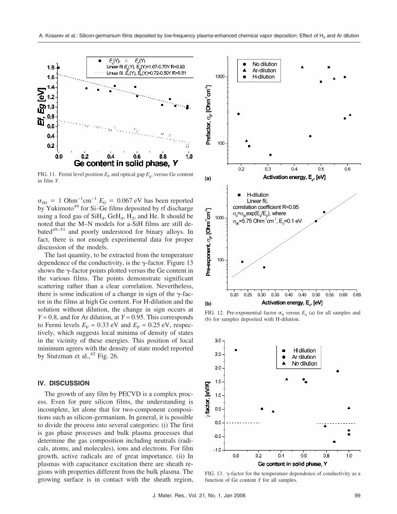
�00 � 1 Ohm−1cm−1 E0 � 0.067 eV has been reportedby Yukimoto49 for Si–Ge films deposited by rf dischargeusing a feed gas of SiH4, GeH4, H2, and He. It should benoted that the M–N models for a-SiH films are still de-bated49–51 and poorly understood for binary alloys. Infact, there is not enough experimental data for properdiscussion of the models.
The last quantity, to be extracted from the temperaturedependence of the conductivity, is the �-factor. Figure 13shows the �-factor points plotted versus the Ge content inthe various films. The points demonstrate significantscattering rather than a clear correlation. Nevertheless,there is some indication of a change in sign of the �-fac-tor in the films at high Ge content. For H-dilution and thesolution without dilution, the change in sign occurs atY ≈ 0.8, and for Ar dilution, at Y ≈ 0.95. This correspondsto Fermi levels EF ≈ 0.33 eV and EF ≈ 0.25 eV, respec-tively, which suggests local minima of density of statesin the vicinity of these energies. This position of localminimum agrees with the density of state model reportedby Stutzman et al.,42 Fig. 26.
IV. DISCUSSION
The growth of any film by PECVD is a complex proc-ess. Even for pure silicon films, the understanding isincomplete, let alone that for two-component composi-tions such as silicon-germanium. In general, it is possibleto divide the process into several categories: (i) The firstis gas phase processes and bulk plasma processes thatdetermine the gas composition including neutrals (radi-cals, atoms, and molecules), ions and electrons. For filmgrowth, active radicals are of great importance. (ii) Inplasmas with capacitance excitation there are sheath re-gions with properties different from the bulk plasma. Thegrowing surface is in contact with the sheath region,
FIG. 12. Pre-exponential factor �0 versus Ea (a) for all samples and(b) for samples deposited with H-dilution.
FIG. 13. �-factor for the temperature dependence of conductivity as afunction of Ge content Y for all samples.
FIG. 11. Fermi level position EF and optical gap Eg, versus Ge contentin film Y.
A. Kosarev et al.: Silicon-germanium films deposited by low-frequency plasma-enhanced chemical vapor deposition: Effect of H2 and Ar dilution
J. Mater. Res., Vol. 21, No. 1, Jan 2006 99

resulting in ion bombardment of the surface. For alter-nating current discharges, electrons bombard the growingsurface during part of the cycle. (iii) Gas–solid processesoccur on the surface of the growing film. Important stepsinclude creation of sites for growth, sticking and desorp-tion, surface diffusion, and surface chemical reactionssuch as hydrogen extraction. The effect of ion bombard-ment is significant and depends on chemical reactivityand mass of the ions, sheath potential, pressure, and dis-charge frequency.52–54 The effect of ion bombardmenthas not been well studied. Nevertheless Dalal et al.55
have reported a positive effect of ion bombardment fordeposition of Si-Ge films by ECR discharge. An increaseof growth rate with Ge in the gas feed was observed byChou and Lee.56 They observed that the growth rateshowed a nearly monotonic increase as X increased from0 to 0.8, followed by reduction as X increased from0.8 to 1.
We observed a monotonic increase of the depositionrate over the entire range of X for the films depositedwith or without H-dilution. The films deposited with Ar-dilution showed a reducing deposition rate in the range Xfrom 0.1 to 0.2 and an increasing rate in the range fromX � 0.2 to 1.0. For the films deposited without dilution,this growth Vd(X) was practically linear, while for H-dilution a trend for Vd to saturate at X > 0.5 was ob-served. The increase of Vd with X has also been reportedin Refs. 38 and 42. In Ref. 56, the authors attempted toexplain this trend by the assumed difference in bindingenergies of Ge–H and Si-H. If the former is less than thelatter, decomposition of GeH4 will be faster, resulting ina higher concentration of Ge radicals, which will thenbecome the more dominating precursors. However, thereis little difference in binding energy calculated from theenthalpy of the hydrogen bonds: 321.7 kJ/mol for Ge–H(Eb� 3.34 eV/bond) and 299.2 kJ/mol for Si–H (Eb�3.1 eV/bond).57 The cross-sections for SiH4 and GeH4
are also not expected to strongly differ since the atomradii are similar: RSi � 1.25 × 10⁻¹⁰ m and RGe � 1.11 ×10⁻¹⁰ m.57 For electron impact decomposition, the electronvelocity relative to the molecule is important, but this alsois practically the same for SiH4 and GeH4 molecules.
The arguments above suggest that the reason for thedeposition rate increase with X might be related to proc-esses on the surface of the growing film, including ionbombardment. For these processes, the difference in Siand Ge masses (mSi � 28 a.u., mGe � 73 a.u.) is of greatimportance. The effect of ion bombardment for the dif-ferent types of dilution (mAr � 40 a.u. and mH � 1 a.u.)is also expected in this case. The two main processes thatoccur on the growing surface are sticking of the precur-sors to the film and surface diffusion of the adsorbedspecies (radicals). The latter is important for structureand properties of the film, while the former significantlyinfluences the film-growth rate. Sticking of each type
of species (radicals) is characterized by the coefficients � Ns/Ntot, where Ns is the number of molecules stuckto the surface, and N is the total number of molecules thatarrived. Conventionally, the SiH3 radical is considered tobe important for the growth of a-SiH films,58 while forSi–Ge growth, a similar principal radical (or radicals) hasnot been revealed. For relatively low Ge concentrations,it is reasonable to consider incorporation of Si atoms inthe lattice in a way similar to amorphous silicon film butnot for incorporation of Ge atoms. The rise in depositionrate with X should be related to Ge atoms and presumablywith the sticking of Ge radicals (atoms). In this case, thefollowing questions should be answered: Why is s forGe-radicals larger than that for Si-radicals? Why doesdilution by H and by Ar affect the deposition rate?
The dependence of Ge content in the film on the Geconcentration in the feed mixture shown in Fig. 3(a) in-dicates clearly preferential incorporation of Ge atoms.Let us introduce the Ge-preference coefficient PGe as
PGe � [Y/(1 − Y)]/[(X/(1 − X)] . (12)
From the best fit of the experimental data as shown forexample in Fig. 3(b) to the theoretical curve (12), weobtain the single parameter of the fit PGe. The result isPGe. � 6.44 ± 0.03 (R � 1) for H-dilution, PGe � 4.3 ±0.6 (R � 0.97) for Ar dilution, and PGe � 3.9 ± 0.2(R � 0.98) for the films deposited without dilution. Pref-erential incorporation of Ge has been reported for rf dis-charge and silane + germane feed gases by Stutzmannet al.42 (PGe � 6 ± 1), and by Chou56 (PGe � 12). Thelatter value reported is remarkably higher than those ob-served in this work, which could be related to differencesin deposition conditions, including discharge frequency,geometry, gas flow, and substrate temperatures. It is in-teresting that the order of the values PGe correlates ininverse fashion with the order of the mass of the domi-nating species. Indeed, we can arrange PGe from maxi-mum to minimum value as PGe� 6.44, 4.3, and 3.9 forthe films deposited with H-and Ar- and without dilution,respectively. The corresponding mass of the dominatingspecies is, of course, MH � 1, MAr � 40, and MGe � 72.During film deposition, there is a sheath potential Usheath
between the growing surface and the bulk plasma. Thispotential accelerates ions moving from the plasma bulkto the growing surface resulting in ion bombardmentwith ion energy Ei ≈ eUsheath. The effect of the ion bom-bardment depends on both Ei and the energy transferefficiency from the ion to the lattice. The efficiency ishighest when the ion mass is equal to that of the latticeatom, while light ions are reflected almost elastically,without energy transfer. This suggests that ion bombard-ment is a significant factor in Ge incorporation.
Another kind of preference that should be discussed isrelated to hydrogen bonding in the films. In a-SiH films,it is well known that the material should have an optimal
A. Kosarev et al.: Silicon-germanium films deposited by low-frequency plasma-enhanced chemical vapor deposition: Effect of H2 and Ar dilution
J. Mater. Res., Vol. 21, No. 1, Jan 2006100

concentration of hydrogen and optimal microstructure,e.g., no Si–H2 bonding, to minimize the concentration ofdangling bonds. For the case of Si–Ge films, there isinsufficient knowledge and understanding of these prob-lems. What is the optimal hydrogen concentration? Howshould hydrogen be distributed between Si and Ge at-oms? What is the optimal microstructure for both Si–Hand Ge–H bonding for achieving good electronic prop-erties? To the knowledge of the authors, there is verylimited information about these questions for films de-posited by the commonly used methods of rf discharge42
and ECR discharge.43 There are no reports on these ques-tions for the films deposited by LF discharge. It shouldbe noted that it is not sufficient just to demonstrate IRspectra indicating significant Ge–H absorption; the lattermust be compared with that for Si–H bonds. Our data inTable II have revealed the effect of gas dilution onthe preference factor of Ge–H bond formation PGe–H
(see Sec. III. D). It should be noted that we observedPGe–H < 1 in all the samples independent of dilution. Thismeans that germanium atoms are terminated with hydro-gen less frequently than silicon atoms. The minimumvalue, PGe–H � 0.29, was observed for the films depos-ited without dilution and the maximum value, PGe–H �0.61, was observed for the films deposited with Ar dilution.
It is interesting to compare the hydrogen distributionbetween Si and Ge atoms and the incorporation of Geatoms. From this comparison, we can see that we have(i) high Ge preference and low Ge–H preference in thefilms with H-dilution, (ii) moderate Ge preference andhigher Ge–H preference in the films deposited with Ardilution, and (iii) low Ge preference together with verylow Ge–H preference in the films deposited without di-lution. In other words, in the case of H-dilution, the filmsgrow with strong preference for Ge incorporation, butthese Ge atoms can create dangling bonds because of lessfrequent termination with hydrogen. When Ar dilution isused, Ge preference is less and Ge–H preference ishigher. Finally, for deposition without dilution, we ob-serve the lowest Ge preference and the lowest Ge–Hpreference, which means that in this case, Ge atoms areincorporated more readily with respect to their propor-tion in the feed gas, but their hydrogen termination isworse. Two other important results from our IR spectraare the dependence of hydrogen and oxygen content inour films upon Ge content. In all the films studied, weobserved reduction in hydrogen content with Y (Fig. 6).The effect of dilution on this trend was not strong. Re-duction of hydrogen with Y has been reported previ-ously59 but without explanation or proposed mechanism.Oxygen content determined by both SIMS and IR wasalso found to decrease with Y (Fig. 7). This trend waspublished previously40 but again without explanation ormechanism for this behavior.
Let us start by considering the dependence of the
optical properties and the optical gap upon Ge content inthe films. A linear dependence of the optical gap on theGe content has been reported for LF discharge: Eg �1.71 − X for X � 0 to 0.5;60 for rf discharge, E04 �1.92 − 0.79Y, Y � 0 to 1.0;38 and for anodic films,18
Eg � 1.76 to 0.78Y61 Eg � 1.73 to 0.71Y.62 In our work,the dependence of the optical gap on Ge content can befitted by Eg � 1.7 to 0.7Y, which is in reasonable agree-ment with the previously reported expressions. The valueof E that characterizes the density of states of the bandtails changed with Ge content and shows a maximum atY ≈ 0.6 for the films deposited with H or Ar dilution. Thiscan presumably be related to the rise of structural disor-der (composition fluctuations) for the films with approxi-mately equal concentrations of Si and Ge atoms. Shenget al.63 have reported long-range fluctuations caused bycompositional disorder for Y > 0.5. Additionally, there isevidence from AFM measurements that for such filmssome peculiarities of Lc(Y) are observed, as indicated inTable I. The increase of the average grain diameter withY for a-Si–Ge films deposited by LF discharge from 81.5to 106 nm has been reported by Budaguan et al.61 Thereasons for the E minimum at Y � 0.45 for the filmsdeposited without dilution is not clear at present butcould be caused by a reduction in tensile stress when Geatoms are incorporated in an optimal concentration. Al-ternatively, processes on the growing surface could beresponsible. In this case, however, one would expectsome features on Vd(Y), which have not been observed.Wickboldt et al.18 found no correlation of E to theoptical gap in Si–Ge films deposited by rf plasma, buttheir experimental data exhibit significant scatter.
The absorption coefficient, �, measured at � �0.63 �m by both optical transmission T(�) and variableangle ellipsometry, exhibits a linear dependence with Y,as shown in Fig. 9. The values obtained by transmissionmeasurements were systematically higher. This can berelated to the fact that T(�) measurements are sensitive tobulk properties, while VAE measurements are more sen-sitive to the sample surface, which can contain an oxidelayer or can otherwise differ from the bulk composition.The refractive index measured by VAE at � � 0.63 �mchanged abruptly from n � 3.91 (characteristic ofa-Si film) to n � 5.4 (characteristic of a-Ge) even at lowY � 0.23. The index of refraction increased further ton � 5.99 at Y � 1.
All specimens exhibited an activation behavior for thetemperature dependence of conductivity �(T), as shownin Fig. 10. The conductivity was observed to increasewith Ge content. Specifically, room temperature conduc-tivity rises by about 7 orders of magnitude and the acti-vation energy reduces, when Y changes from 0 to 1. It isinteresting to compare the behavior of the Fermi levelposition EF, and the band gap EG with Ge content, asshown in Fig. 11. Here, the Fermi level behavior can be
A. Kosarev et al.: Silicon-germanium films deposited by low-frequency plasma-enhanced chemical vapor deposition: Effect of H2 and Ar dilution
J. Mater. Res., Vol. 21, No. 1, Jan 2006 101

fit to a linear dependence: EF(Y) � 0.72 − 0.50Y. Bycomparing EF(Y) to EG(Y), it can be concluded that theFermi level moves from approximately mid-gap for Y � 0to the edge of the conduction band with increasing Y;i.e., the films become more n-type. However, Wickboldtet al.18 reported no shift of EF with Y for the films de-posited by rf discharge. Nonlinear behavior of the Fermilevel position with Ge content has been reported in Ref.38. The behavior of the conductivity prefactor and �-fac-tor is discussed in Sec. III. F.
V. CONCLUSIONS
Deposition processes, structure, and optical and elec-trical properties have been studied in Si1−YGeY:H filmsdeposited by LF PECVD over the entire range of com-positions (0 � Y � 1) from SiH4 and GeH4 feed gasmixtures with and without dilution by hydrogen or byargon. From the observations and data analysis we candraw the following conclusions:
(1) Dilution by hydrogen or by argon decreases thedeposition rate. The deposition rate increases with Gecontent.
(2) Ge atoms are preferentially incorporated accord-ing to a preference factor PGe, ranging from a maximumof 6.44 for deposition with hydrogen dilution to a mini-mum of 3.9 for the films deposited without dilution.
(3) For all films, the hydrogen content decreases as Yincreases. Similar behavior is observed for oxygen.
(4) Hydrogen preferentially terminates at Si atoms. Thepreferential factor PGe–H � 0.29 for no dilution (the worstcase) and PGe–H � 0.61 for argon dilution (the best case).
(5) The optical gap decreases linearly with Ge contentto as small as Eg ≈ 0.92 to 0.95 eV at Y � 1 (a-Ge).
(6) The energy characterized band tail states Eachieves a maximum at Y ≈ 0.6 in the films depositedwith hydrogen or argon dilution and continuously in-creases with Y for the films deposited without dilution.
(7) The optical constants measured by VAE (a surfacesensitive technique) are in reasonable agreement withpublished data. The absorption coefficient and the refrac-tive index obtained by VAE in comparison with dataobtained from spectral transmission measurements (abulk sensitive technique) suggest the films contain a sur-face layer with oxides and pores.
(8) Ge content increases the conductivity of the filmsby about 7 orders of magnitude. Ge also reduces theactivation energy for �(T). The effect of Ge on the tem-perature dependence depends on the amount and speciesof dilution.
(9) The Fermi level position changes approximatelylinearly with Y. Comparing this behavior with that of theoptical gap suggests the Fermi level shifts from about themiddle of the gap at low Y to the conduction band edgeat high Y, i.e., the films become more n-type as Ge isincorporated.
(10) The conductivity pre-exponential �0 does notshow a correlation with activation energy, i.e., there is noevidence for an analog to the Neyer–Mendel rule foundfor amorphous silicon.
(11) The conductivity �-factor changes sign at Y � 0.8for deposition with or without H-dilution and at Y � 0.95for Ar dilution. This suggests local minima in the density ofstates at E ≈ 0.33eV and at E ≈ 0.25 eV for the two cases.
ACKNOWLEDGMENT
The co-authors from Institut Nacional de Astrofisica,Optica y Electronica acknowledge the support of thisresearch by Consejo Nacional de Ciencia y TecnologıaProject No. 42367 (Colaboracion Inter-Americana enMateriales-2002 Program). Work by T.E.F. was per-formed under the auspices of the United States Depart-ment of Energy by the University of California LawrenceLivermore National Laboratory under Contract No.W-7405-Eng-48.
REFERENCES1. J.K. Rath, F.D. Tichelaar, and R.E.I. Schropp: Heterogeneous
growth of microcrystalline silicon germanium. Sol. Energy Mater.Sol. Cells 74, 533 (2002).
2. M. Isomura, K. Nakahata, M. Shima, S. Taira, K. Wakisaka,M. Tanaka, and S. Kiyama: Microcrystalline silicon–germaniumsolar cells for multi-junction structures. Sol. Energy Mater.Sol. Cells 74, 519 (2002).
3. M. Krause, H. Stiebig, R. Carius, and H. Wagner: Microcrystal-line germanium photodetectors, in Amorphous and HeterogeneousSilicon-Based Films—2001, edited by M. Stutzman, J.B. Boyce,J.D. Cohen, R.W. Collins, and J. Hanna (Mater. Res. Soc. Symp.Proc. 664, Warrendale, PA, 2001), p. A26.5.
4. G. Masini, V. Cencelli, L. Colace, F. DeNotaristefani, andG. Assanto: A germanium photodetector array for the near infra-red monolithically integrated with silicon CMOS readout elec-tronics. Physica E 16, 614 (2003).
5. R. Ambrosio, A. Torres, A. Kosarev, A. Heredia, and M. Garcia:Amorphous Si1−yGey:H,F films obtained by low frequencyPECVD for uncooled microbolometers, in Amorphous andNanocrystalline Silicon Science and Technology—2004, edited byG. Ganguly, M. Kondo, E.A. Schiff, R. Carius, and R. Biswas.(Mater. Res. Soc. Symp. Proc. 808, Warrendale, PA, 2004),p. A4.29.
6. A. Torres, A. Kosarev, M.L. Garcia, and R. Ambrosio: Uncooledmicro-bolometer based on amorphous germanium film. J. Non-Cryst. Solids 329, 179 (2003).
7. M. Garcia, R. Ambrosio, A. Torres, and A. Kosarev: IR bolom-eters based on amorphous silicon germanium alloys. J. Non-Cryst.Solids 338–340, 744 (2004).
8. W.B. Jordan and S. Wagner: Nanocrystalline germanium p-i-nstructures, in Amorphous and Nanocrystalline Silicon Science andTechnology—2004, edited by G. Ganguly, M. Kondo, E.A. Schiff,R. Carius, and R. Biswas (Mater. Res. Soc. Symp. Proc. 808,Warrendale, PA, 2004), p. A9.47.
9. W. Luft and Y.S. Tsuo: Hydrogenated Amorphous Silicon AlloyDeposition Processes (Marcel Dekker, New York 1993).
10. T. Searle: Properties of amorphous silicon and its alloys. EMISDatareviews Series No. 19, INSPEC, The Institution of ElectricalEngineers, London, United Kingdom, 1998.
11. Y. Liu and V.L. Dalal: Properties of amorphous silicon-
A. Kosarev et al.: Silicon-germanium films deposited by low-frequency plasma-enhanced chemical vapor deposition: Effect of H2 and Ar dilution
J. Mater. Res., Vol. 21, No. 1, Jan 2006102

germanium films and devices deposited at higher growth rates, inAmorphous and Heterogeneous Silicon-Based Films—2002, ed-ited by J.D. Cohen, J.R. Abelson, H. Matsumura, and J. Robertson(Mater. Res. Soc. Symp. Proc. 715, Warrendale, PA, 2002),p. A18.3.
12. H. Matsumura, M. Yamaguchi, and K. Morigaki: Properties ofcatalytic CVD amorphous silicon germanium (a-SiGe:H), inAmorphous Silicon Technology—1990, edited by P.C. Taylor,M.J. Thompson, P.G. LeComber, Y. Hamakawa, and A. Madan(Mater. Res. Soc. Symp. Proc. 192, Pittsburgh, PA, 1990), p. 499.
13. V.L. Dalal, Y. Liu, Z. Zhou, and K. Han: Growth and propertiesof low bandgap amorphous (Si, Ge) alloy materials and devices.J. Non-Cryst. Solids 299–302, 1127 (2002).
14. M.A. Lieberman and A.J. Lichtenberg: Principles of Plasma Dis-charges and Material Processing (J. Wiley and Sons, New York,1994), p. 333.
15. B.G. Budagian, A.A. Sherechenkov, G.L. Gorbulin, andV.D. Chernomordic: Characterization of high rate a-SiGe:H thinfilms fabricated by 55 kHz PECVD. Physica B 325, 394 (2003).
16. K.D. Mackenzie, J.R. Eggert, D.J. Leopold, Y.M. Li, S. Lin, andW. Paul: Structural, electrical, and optical properties ofa-Si1−xGex:H and an inferred electronic band structure. Phys. Rev.B 31, 2198 (1985).
17. Y. Liu and V.L. Dalal: Properties of amorphous silicon-germanium films and devices deposited at higher growth rates, inAmorphous and Heterogeneous Silicon Based Films—2002, ed-ited by J.D. Cohen, J.R. Abelson, H. Matsumura, and J. Robertson(Mater. Res. Soc. Symp. Proc. 715, Warrendale, PA, 2002),p. A18.3.
18. P. Wickboldt, D. Pang, W. Paul, J.H. Chen, F. Zhong, C.C. Chen,J.D. Cohen, and L. Williamson: High performance glow dischargea-Si1−xGex:H of large x. J. Appl. Phys. 81, 6252 (1997).
19. Y.S. Tsuo, Y. Xu, E.A. Ramsay, R.S. Crandall, S.J. Salamon,I. Balberg, B.P. Nelson, Y. Xiao, and Y. Chen: Methods of im-proving glow-discharge-deposited a-SiGe, in Amorphous SiliconTechnology—1991, edited by A. Madan, Y. Hamakawa, M.J.Thompson, P.C. Taylor, and P.G. LeComber (Mater. Res. Soc.Symp. Proc. 219, Pittsburgh, PA, 1991), p. 769.
20. M. Shima, A. Terakawa, M. Isomura, H. Haku, M. Tanaka,K. Wakisaka, S. Kiyama, and S. Tsuda: Effects of very high hy-drogen dilution at low temperature on hydrogenated amorphoussilicon germanium. J. Non-Cryst. Solids 227–230, 442 (1998).
21. S. Miyazaki, H. Takahashi, H. Yamashita, and M. Hirose: Growthand characterization of microcrystalline silicon–germanium films.J. Non-Cryst. Solids 299–302, 148 (2002).
22. M.E. Gueunier, J.P. Kleider, R. Bruggemann, S. Lebib, P. Roca,I. Cabarrocas, R. Meaudre, and B. Canut: Properties of polymor-phous silicon–germanium alloys deposited under high hydrogendilution and at high pressure. J. Appl. Phys. 92, 4959 (2002).
23. W.B. Jordan and S. Wagner: Effects of deposition temperatureand film thickness on the structural, electrical, and optical prop-erties of germanium thin films, in Amorphous and HeterogeneousSilicon Based Films—2002, edited by J.D. Cohen, J.R. Abelson,H. Matsumura, and J. Robertson (Mater. Res. Soc. Symp. Proc.715, Warrendale, PA, 2002), p. A18.2.
24. M.H. Brodsky, M. Cardona, and J.C. Cuomo: Infrared and Ramanspectra of the silicon-hydrogen bonds in amorphous silicon pre-pared by glow discharge and sputtering. Phys. Rev. B 16, 3556(1977).
25. R. Swanepoel: Determination of the thickness and optical con-stants of amorphous silicon. J. Phys. E. Sci. Instrum. 16, 1214(1983).
26. R. Swanepoel: Determination of surface roughness and opticalconstants of inhomogeneous amorphous silicon films. J. Phys. E.Sci. Instrum. 17, 896 (1984).
27. Y. Zhao, G-C. Wang, and T-M. Lu: Characterization of Amor-phous and Crystalline Rough Surface: Principles and Applica-tions (Academic Press Inc., Reading, MA 2001), pp. 7–16.
28. D. Comedi, F. Dondeo, I. Chambouleyron, Z.L. Peng, andP. Masher: Compact hydrogenated amorphous germanium filmsby ion-beam sputtering deposition. J. Non-Cryst. Solids 266–269,713 (2000).
29. G. Lukovsky, S.S. Chao, J. Yang, J.E. Tyler, R.C. Ross, andW. Czubatyj: Chemical bonding of hydrogen and oxygen in glow-discharge–deposited thin films of a-Ge:H and a-Ge:(H,O). Phys.Rev. B 31, 2190 (1985).
30. M.N. Makadzi, M.F.A. Alias, A.A. Essa, and H.R. Al-Azawi: FT-IR and XPS analysis of a-Si1−xGex:H thin films. Renewable En-ergy 28, 975 (2003).
31. G. Lukovsky, J. Yang, S.S. Chao, J.E. Tyler, and W. Chubatyj: IRabsorption in glow-discharge-deposited a-Si:(D,O) and a-Si:(D,N)alloy films. Phys. Rev. B 29, 2302 (1984).
32. G. Lukovsky and J.D. Joannopoulos: The Physics of Hydroge-nated Amorphous Silicon (VII, Springer, Berlin, Germany, 1984),p. 235
33. C.J. Fang, R.J. Gruntz, L. Ley, M. Cardona, F.J. Demond,G. Muller, and S. Kalbitzer: The hydrogen content of a-Ge:H anda-Si:H as determined by IR spectroscopy, gas evolution andnuclear reaction techniques. J. Non-Cryst. Solids 35–36, 255(1980).
34. W. Beyer: Diffusion and solubility of hydrogen in amorphous andmicrocrystalline Si:H films, in Amorphous and HeterogeneousSilicon-Based Films—2001, edited by M. Stutzmann, J.B. Boyce,J.D. Cohen, R.W. Collins, and J. Hanna (Mater. Res. Soc. Symp.Proc. 664, Warrendale, PA, 2001), p. A13.1..
35. W.A. Lanford, H.P. Trautvetter, J.F. Ziegler, and J. Keller: Newprecision technique for measuring the concentration versus depthof hydrogen in solids. Appl. Phys. Lett. 28, 566 (1976).
36. R.C. Ross, I.S.T. Tsongm, R. Messier, W.A. Lanford, andC. Burman: Quantification of hydrogen in a-Si:H films by IRspectrometry, N nuclear reaction, and SIMS. J. Vac. Sci. Technol.20, 406 (1982).
37. M. Cardona: Vibrational-spectra of hydrogen in silicon and ger-manium. Phys. Status Solidi B 118, 463 (1983).
38. K.D. Mackenzie, J.R. Eggert, D.J. Leopold, Y.M. Li, S. Lin,and W. Paul: Structural, electrical, and optical properties ofa-Si1−xGex:H and an inferred electronic band structure. Phys. Rev.B 31, 2198 (1985).
39. A.A. Langford, M.L. Fleet, B.P. Nelson, and N. Maley: Infraredabsorption strength and hydrogen content of hydrogenated amor-phous silicon. Phys. Rev. B 45, 13367 (1992).
40. B.P. Nelson, Y. Xu, J.D. Webb, A. Mason, R.C. Reedy,L.M. Gedvilas, and W.A. Lanford: Techniques for measuring thecomposition of hydrogenated amorphous silicon–germanium al-loys. J. Non-Cryst. Solids 266–269, 680 (2000).
41. W. Paul, D.K. Paul, B. Von Roedern, J. Blake, and S. Oguz: Pref-erential attachment of H in amorphous hydrogenated binary semi-conductors and consequent inferior reduction of pseudogap statedensity. Phys. Rev. Lett. 46, 1016 (1981).
42. M. Stutzmann, R.A. Street, C.C. Tsai, J.B. Boyce, and S.E. Ready:Structural, optical, and spin properties of hydrogenated amor-phous silicon-germanium alloys. J. Appl. Phys. 66, 569 (1989).
43. V.L. Dalal: Growth chemistry of amorphous silicon and amor-phous silicon-germanium alloys. Curr. Opin. Solid State Mater.Sci. 6, 455 (2002).
44. N.F. Mott and E.A. Davis: Electronic Processes in Non-Crystalline Materials (Clarendon Press, Oxford, U.K., 1979).
45. Handbook of Optical Constants of Solids II, edited by E. Palik(Academic Press Inc., Reading, MA), p. 774.
A. Kosarev et al.: Silicon-germanium films deposited by low-frequency plasma-enhanced chemical vapor deposition: Effect of H2 and Ar dilution
J. Mater. Res., Vol. 21, No. 1, Jan 2006 103

46. R.F. Potter: Optical constants of germanium in spectral regionfrom 0.5 to 3.0 eV. Phys. Rev. 150, 562 (1966).
47. P. Nagels: In Amorphous Silicon, edited by M.H. Brodsky(Springer, New York, 1979), p. 122.
48. D.E. Carlson and C.R. Wronski: Amorphous silicon solar cells, inAmorphous Semiconductors, edited by M.H. Brodsky (Springer,New York, 1979), Chap. 10, p. 299.
49. Y. Yukimoto: Hydrogenated a-Si-Ge alloy and its aoptoelectronicin JARECT v: 6 Amorphous Semiconductor Technologies anddevices, edited by Y. Hamakawa, (1983), p. 136.
50. W.B. Jackson: Connection between the Meyer–Neldel relationand multiple-trapping transport. Phys. Rev. B 38, 3595 (1988).
51. M. Kikuchi: The Meyer–Neldel rule and the statistical shift of theFermi level in amorphous semiconductors. J. Appl. Phys. 64, 4997(1988).
52. P. Roca i Canbarrocas, P. Morrin, V. Chu, J.P. Conde, J.Z. Liu,H.R. Park, and S. Wagner: Optoelectronic properties of hydroge-nated amorphous silicon films deposited under negative substratebias. J. Appl. Phys. 69, 2942 (1991).
53. B. Kalache, A.I. Kosarev, R. Vanderhagen, and P. Roca i Cabarrocas:Ion bombardment effects on microcrystalline silicon growth mecha-nisms and on the film properties. J. Appl. Phys. 93, 1262 (2003).
54. E.A.G. Hammers, A. Fontcuberta, I. Morral, C. Niikura, R. Brenot,and P. Roca I Cabarrocas: Contribution of ions to the growth ofamorphous, polymorphous, and microcrystalline silicon thinfilms. J. Appl. Phys. 88, 3674 (2000).
55. V.L. Dalal, S. Haroon, Z. Zhou, T. Maxson, and K. Han: Influ-ence of plasma chemistry on the properties of a-(Si,Ge):H alloys.J. Non-Cryst Solids 266, 675 (2000).
56. Y-P. Chou and S-C. Lee: Structural, optical, and electrical prop-erties of hydrogenated amorphous silicon germanium alloys.J. Appl. Phys. 83, 4111 (1998).
57. www.webelements.com
58. A. Matsuda: Plasma and surface reactions for obtaining low defectdensity amorphous silicon at high growth rates. J. Vac. Sci. Tech-nol. A 16, 365 (1998).
59. Y.T. Simizu, M. Kumeda, A. Morimoto, Y. Tsujimura, andI. Kobayashi: NMR and ESR studies on a-SiGe:H films preparedby glow discharge and magnetron sputtering, in Materials Issuesin Amorphous-Semiconductor Technology, edited by D. Adler, Y.Hamakawa, and A. Madan (Mater. Res. Symp. Proc. 70, 1986),p. 313.
60. B.G. Budaguan, A.A. Sherchenkov, and G.L. Gorbulin: The prop-erties of a-SiGe:H films deposited by 55 kHz PECVD. J. Non-Cryst Solids 297, 205 (2002).
61. K.D. Mackenzie, J.H. Burnett, J.R. Eggert, Y.M. Li, and W. Paul:Comparison of the structural, electrical, and optical properties ofamorphous silicon-germanium alloys produced from hydrides andfluorides. Phys. Rev. B38, 6120 (1988).
62. K.D. Mackenzi, J. Hanma, J.R. Eggert, Y.M. Li, Z.L. Sun, andW. Paul: Properties of a-Si1−xGex:H and a-Si1−xGex:H:F alloys.J. Non-Cryst. Solids 77–78, 881 (1985).
63. S.R. Sheng, M. Boshta, R. Braunstein, and V. Dalal: On the elec-tronic transport properties of amorphous (Si,Ge) alloys: Chargedscattering centers and compositional disorder. J. Non-Cryst. Solids303, 201 (2002).
A. Kosarev et al.: Silicon-germanium films deposited by low-frequency plasma-enhanced chemical vapor deposition: Effect of H2 and Ar dilution
J. Mater. Res., Vol. 21, No. 1, Jan 2006104