signal constellation distortion and ber …signal constellation distortion and ber degradation due...
TRANSCRIPT
Progress In Electromagnetics Research, Vol. 121, 225–247, 2011
SIGNAL CONSTELLATION DISTORTION AND BERDEGRADATION DUE TO HARDWARE IMPAIRMENTSIN SIX-PORT RECEIVERS WITH ANALOG I/Q GENER-ATION
A. Moscoso-Martir*, I. Molina-Fernandez, andA. Ortega-Monux
Departmento de Ingenieria de Comunicaciones, ETSI Telecomuni-cacion, Malaga University, Campus Universitario de Teatinos s/n,Malaga 29011, Spain
Abstract—Since its introduction in 1994 direct conversion six-port receivers have attracted a considerable attention at microwavefrequencies, with most recent work focusing on the so called six-port receivers with analog I/Q generation. Besides its applicationsat microwave frequencies, six-port receivers with I/Q regenerationplay a crucial role in the optical communications field, as they arethe most promising candidates for optical coherent receivers that arebeing developed for 100 Gigabit Ethernet transceivers. In this paperwe analytically model the influence of six-port junction hardwareimpairments on receiver performance. New analytical expressions aredeveloped which give geometrical interpretation of signal constellationdistortion due to hardware impairments and allow for the definition ofseveral interesting figures of merit. Closed formulas are also proposedto analytically calculate BER degradation, under AWGN conditions,from these figures of merit. Finally, the proposed formulas arevalidated by means of simulation, and it is shown that they can beof practical interest to set the specifications of the six-port junctioncomponents.
1. INTRODUCTION
Modern wireless microwave receiver design demands increasedbandwidth with reduced size and cost. Since its introduction in 1994 [1]direct conversion six-port receivers have attracted a considerable
Received 8 July 2011, Accepted 28 September 2011, Scheduled 25 October 2011* Corresponding author: Alvaro Moscoso-Martir ([email protected]).
226 Moscoso-Martir, Molina-Fernandez, and Ortega-Monux
attention at microwave frequencies [2–4] as they offer lower hardwarecomplexity, lower local oscilator (LO) power, and higher bandwidthwhen compared with other alternatives that make use of active mixers.Besides, six-port based direct detection receivers are nowadays ahot topic in the optical community as they are the most promisingcandidates for modern 100 Gb/s coherent optical receivers [5–7].
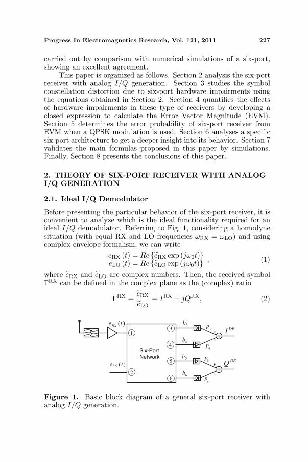
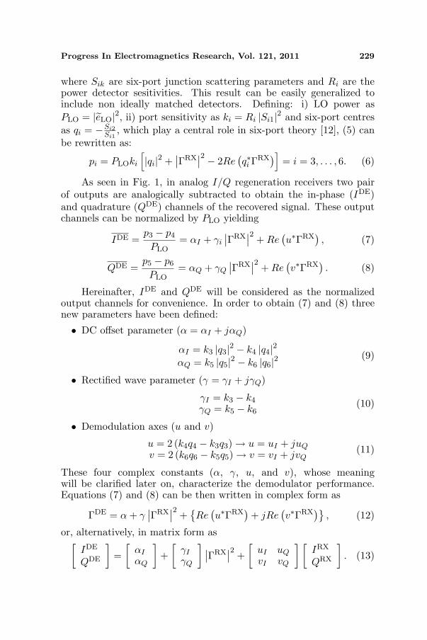
Figure 1 shows the basic building blocks of a six-port receiver:the six-port passive junction and the four power detectors. The six-port passive junction combines the reference signal, generated by thelocal oscillator (LO), and the received radio frequency (RX) signal,with specific amplitude and phase relations at the input of the fourpower detectors. Six-port receivers are usually designed to work inhomodyne operation, so that, the power detector outputs are directlyobtained in baseband, and the I/Q signals can be recovered by analogor digital means. In the first six-port receiver proposals [1] the fourpower detectors outputs were digitized, which enabled the use ofpowerful calibration strategies to remove hardware imperfections [8].However, more recently, analog I/Q generation has become thepreferred alternative. It offers the advantage of providing a simpleanalog solution at the cost of requiring a much more demandinghardware design (as no calibration is available).
Several papers have studied the performance and features of six-port receiver with analog I/Q generation in multiple situations. In [9]the six-port receiver is theoretically described and compared with thehomodyne and heterodyne reception architectures. In [10] the analysisis focused on the relationship between the LO power level and systemlevel parameters of the receiver with an ideal six-port network. Finally,in [11] the diode power detector behavior in a six-port communicationsreceiver is studied using an ideal six-port network. However, up tothe authors’ knowledge, a complete study of the influence of six-portjunction hardware impairments on receiver performance has not beenreported yet.
The goal of this paper is to make a detailed study of theperformance degradation of analog I/Q generation six-port receiversdue to hardware imperfections of the six-port passive junction. Idealsquare law power detector behaviour is considered throughout thiswork. Compact expressions are obtained that give a deeper insightinto the mechanisms causing receiver degradation due to hardwareimpairments. Furthermore, they allow to easily calculate the ErrorVector Magnitude (EVM) and to set hardware specifications tofulfill the design requirements. Specific theoretical formulas are alsopresented to calculate Bit Error Rate (BER) degradation for a QPSKmodulation scheme. Finally, assessment of the proposed formulas is
Progress In Electromagnetics Research, Vol. 121, 2011 227
carried out by comparison with numerical simulations of a six-port,showing an excellent agreement.
This paper is organized as follows. Section 2 analysis the six-portreceiver with analog I/Q generation. Section 3 studies the symbolconstellation distortion due to six-port hardware impairments usingthe equations obtained in Section 2. Section 4 quantifies the effectsof hardware impairments in these type of receivers by developing aclosed expression to calculate the Error Vector Magnitude (EVM).Section 5 determines the error probability of six-port receiver fromEVM when a QPSK modulation is used. Section 6 analyses a specificsix-port architecture to get a deeper insight into its behavior. Section 7validates the main formulas proposed in this paper by simulations.Finally, Section 8 presents the conclusions of this paper.
2. THEORY OF SIX-PORT RECEIVER WITH ANALOGI/Q GENERATION
2.1. Ideal I/Q Demodulator
Before presenting the particular behavior of the six-port receiver, it isconvenient to analyze which is the ideal functionality required for anideal I/Q demodulator. Referring to Fig. 1, considering a homodynesituation (with equal RX and LO frequencies ωRX = ωLO) and usingcomplex envelope formalism, we can write
eRX (t) = Re {eRX exp (jω0t)}eLO (t) = Re {eLO exp (jω0t)} , (1)
where eRX and eLO are complex numbers. Then, the received symbolΓRX can be defined in the complex plane as the (complex) ratio
ΓRX =eRX
eLO= IRX + jQRX, (2)
1
2
3
4
5
6
b
b
b
b
LOe
RXe
DEI
p
p
p
p
DE
Six-Port
Network
t
t
3
Q
3
4
4
55
6
6
( )( )
( )
Figure 1. Basic block diagram of a general six-port receiver withanalog I/Q generation.
228 Moscoso-Martir, Molina-Fernandez, and Ortega-Monux
1
1U
Uje
planeRX
planeDE
Γ Γφ
UUjeφ
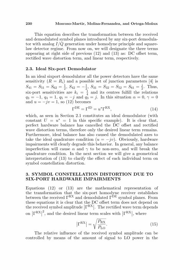
Figure 2. Transformation between the received (ΓRX) anddemodulated (ΓDE) symbol planes caused by the demodulator in anideal situation.
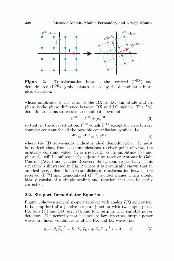
whose amplitude is the ratio of the RX to LO amplitude and itsphase is the phase difference between RX and LO signals. The I/Qdemodulator aims to recover a demodulated symbol
ΓDE = IDE + jQDE (3)
so that, in the ideal situation, ΓDE equals ΓRX except for an arbitrarycomplex constant for all the possible constellation symbols, i.e.,
ΓID = ΓDE = U ΓRX (4)
where the ID super-index indicates ideal demodulation. It mustbe noticed that, from a communications receiver point of view, thearbitrary constant value, U , is irrelevant, as its amplitude |U | andphase φU will be subsequently adjusted by receiver Automatic GainControl (AGC) and Carrier Recovery Subsystem, respectively. Thissituation is illustrated in Fig. 2 where it is graphically shown that inan ideal case, a demodulator establishes a transformation between thereceived (ΓRX) and demodulated (ΓDE) symbol planes which shouldideally consist of a simple scaling and rotation that can be easilycorrected.
2.2. Six-port Demodulator Equations
Figure 1 shows a general six-port receiver with analog I/Q generation.It is comprised of a passive six-port junction with two input ports,RX (eRX (t)) and LO (eLO (t)), and four outputs with suitable powerdetectors. For perfectly matched square law detectors, output powerwaves are linear combinations of the RX and LO waves, i.e.,
pi = Ri
∣∣∣bi
∣∣∣2
= Ri |Si1eRX + Si2eLO|2 i = 3, . . . , 6, (5)
Progress In Electromagnetics Research, Vol. 121, 2011 229
where Sik are six-port junction scattering parameters and Ri are thepower detector sesitivities. This result can be easily generalized toinclude non ideally matched detectors. Defining: i) LO power asPLO = |eLO|2, ii) port sensitivity as ki = Ri |Si1|2 and six-port centresas qi = −Si2
Si1, which play a central role in six-port theory [12], (5) can
be rewritten as:
pi = PLOki
[|qi|2 +
∣∣ΓRX∣∣2 − 2Re
(q∗i Γ
RX)]
= i = 3, . . . , 6. (6)
As seen in Fig. 1, in analog I/Q regeneration receivers two pairof outputs are analogically subtracted to obtain the in-phase (IDE)and quadrature (QDE) channels of the recovered signal. These outputchannels can be normalized by PLO yielding
IDE =p3 − p4
PLO= αI + γi
∣∣ΓRX∣∣2 + Re
(u∗ΓRX
), (7)
QDE =p5 − p6
PLO= αQ + γQ
∣∣ΓRX∣∣2 + Re
(v∗ΓRX
). (8)
Hereinafter, IDE and QDE will be considered as the normalizedoutput channels for convenience. In order to obtain (7) and (8) threenew parameters have been defined:
• DC offset parameter (α = αI + jαQ)
αI = k3 |q3|2 − k4 |q4|2αQ = k5 |q5|2 − k6 |q6|2 (9)
• Rectified wave parameter (γ = γI + jγQ)
γI = k3 − k4
γQ = k5 − k6(10)
• Demodulation axes (u and v)
u = 2 (k4q4 − k3q3) → u = uI + juQ
v = 2 (k6q6 − k5q5) → v = vI + jvQ(11)
These four complex constants (α, γ, u, and v), whose meaningwill be clarified later on, characterize the demodulator performance.Equations (7) and (8) can be then written in complex form as
ΓDE = α + γ∣∣ΓRX
∣∣2 +{Re
(u∗ΓRX
)+ jRe
(v∗ΓRX
)}, (12)
or, alternatively, in matrix form as[
IDE
QDE
]=
[αI
αQ
]+
[γI
γQ
] ∣∣ΓRX∣∣2 +
[uI uQ
vI vQ
] [IRX
QRX
]. (13)
230 Moscoso-Martir, Molina-Fernandez, and Ortega-Monux
This equation describes the transformation between the receivedand demodulated symbol planes introduced by any six-port demodula-tor with analog I/Q generation under homodyne principle and square-law detector regime. From now on, we will designate the three termsappearing at right side of previous (12) and (13) as: DC offset term,rectified wave distortion term, and linear term, respectively.
2.3. Ideal Six-port Demodulator
In an ideal sixport demodulator all the power detectors have the samesensitivity (R = Ri) and a possible set of junction parameters [4] isS41 = S51 = S62 = 1
2 , S42 = −12 , S31 = S32 = S52 = S61 = j
2 . Thus,six-port sensitivities are ki = 1
4 and its centres fulfill the relationsq3 = −1, q4 = 1, q5 = −j and q3 = j. In this situation α = 0, γ = 0and u = −jv = 1, so (12) becomes
ΓDE = ΓID = u∗ΓRX, (14)which, as seen in Section 2.1 constitutes an ideal demodulator (withconstant U = u∗ = 1 in this specific example). It is clear that,perfect hardware balance has cancelled the DC offset and rectifiedwave distortion terms, therefore only the desired linear term remains.Furthermore, ideal balance has also caused the demodulated axes totake the ideal quadrature condition (u = −jv). Obviously, hardwareimpairments will clearly degrade this behavior. In general, any balanceimperfection will cause α and γ to be non-zero, and will break thequadrature condition. In the next section we will give a geometricalinterpretation of (13) to clarify the effect of each individual term onsymbol constellation distortion.
3. SYMBOL CONSTELLATION DISTORTION DUE TOSIX-PORT HARDWARE IMPAIRMENTS
Equations (12) or (13) are the mathematical representation ofthe transformation that the six-port homodyne receiver establishesbetween the received ΓRX and demodulated ΓDE symbol planes. Fromthese equations it is clear that the DC offset term does not depend onthe received symbol amplitude
∣∣ΓRX∣∣. The rectified wave term depends
on∣∣ΓRX
∣∣2, and the desired linear term scales with∣∣ΓRX
∣∣, where
∣∣ΓRX∣∣ =
√PRX
PLO. (15)
The relative influence of the received symbol amplitude can becontrolled by means of the amount of signal to LO power in the

Progress In Electromagnetics Research, Vol. 121, 2011 231
demodulator: DC offset (due to α 6= 0) will dominate for low PRX/PLO
ratio, while rectified wave distortion (due to γ 6= 0) will dominate forhigh PRX/PLO ratio. As a consequence, proper operation of a realsix-port will only be possible in some range of PRX/PLO ratios andthis will intrinsically limit the receiver’s dynamic range. Please noticethat this effect happens even under ideal square-law detection regimeand it is only due to linear imbalances in the sixport junction anddetector sensitivities, so it must not be confused with dynamic rangelimitations coming from higher order nonlinearities of power detectorsas analyzed in [13]. This limitation will be of practical importancein optical communication receivers [6], where diode photodetector areintrinsically square law devices and thus dynamic range limitations areexpected to appear due to six-port junction impairments.
Once the relative weights of terms appearing in (12) and (13) havebeen discussed, we will focus on geometrical interpretation of receiverimpairments.
3.1. Constellation Distortion due to Linear Impairments
From (13) it is obvious that DC offset and linear terms have a simpleinterpretation. Effectively, setting γ = 0, (13) becomes
[IDE
QDE
]=
[αI
αQ
]+
[uI uQ
vI vQ
] [IRX
QRX
]. (16)
Figure 3 shows the effects of this transformation consisting of atranslation α of the origin of coordinates followed by a rotation andimbalance of reference axes.
Re ( ) RX Re ( )DE
Im (
)
RX
Im (
)
DE
Figure 3. Constellation distortion due to linear impairments in thesix-port receiver.
232 Moscoso-Martir, Molina-Fernandez, and Ortega-Monux
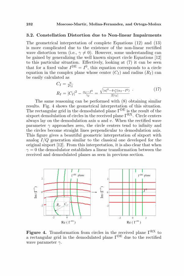
3.2. Constellation Distortion due to Non-linear Impairments
The geometrical interpretation of complete Equations (12) and (13)is more complicated due to the existence of the non-linear rectifiedwave distortion term (i.e., γ 6= 0). However, some understanding canbe gained by generalizing the well known sixport circle Equations [12]to this particular situation. Effectively, looking at (7) it can be seenthat for a fixed value IDE = I0, this equation corresponds to a circleequation in the complex plane whose center (CI) and radius (RI) canbe easily calculated as
CI = u2γI
RI = |CI |2 − αI−I0
γI=
√|u|2−4γ∗I (αI−I0)
2|γI |. (17)
The same reasoning can be performed with (8) obtaining similarresults. Fig. 4 shows the geometrical interpretation of this situation.The rectangular grid in the demodulated plane ΓDE is the result of thesixport demolulation of circles in the received plane ΓRX. Circle centersalways lay on the demodulation axis u and v. When the rectified waveparameter γ approaches zero, the circle centers tend to infinity andthe circles become straight lines perpendicular to demodulation axis.This figure gives a beautiful geometric interpretation of sixport withanalog I/Q generation similar to the classical one developed for theoriginal sixport [12]. From this interpretation, it is also clear that whenγ = 0 the demodulator establishes a linear transformation between thereceived and demodulated planes as seen in previous section.
Re ( Γ )RX
Re ( Γ )DE
Im (
)
ΓR
X
Im (
)
ΓD
E
-2 0 2 -2 0 2
2
0
-2
2
0
-2
planeΓRX planeΓ
DE
Figure 4. Transformation from circles in the received plane ΓRX toa rectangular grid in the demodulated plane ΓDE due to the rectifiedwave parameter γ.
Progress In Electromagnetics Research, Vol. 121, 2011 233
4. ERROR VECTOR MAGNITUDE DUE TO SIX-PORTHARDWARE IMPAIRMENTS
In this section we will quantify the effects of constellation distortionon demodulator performance by developing a closed expression tocalculate the Error Vector Magnitude [14] (EVM) from sixportparameters α, γ, u and v in (9)–(11).
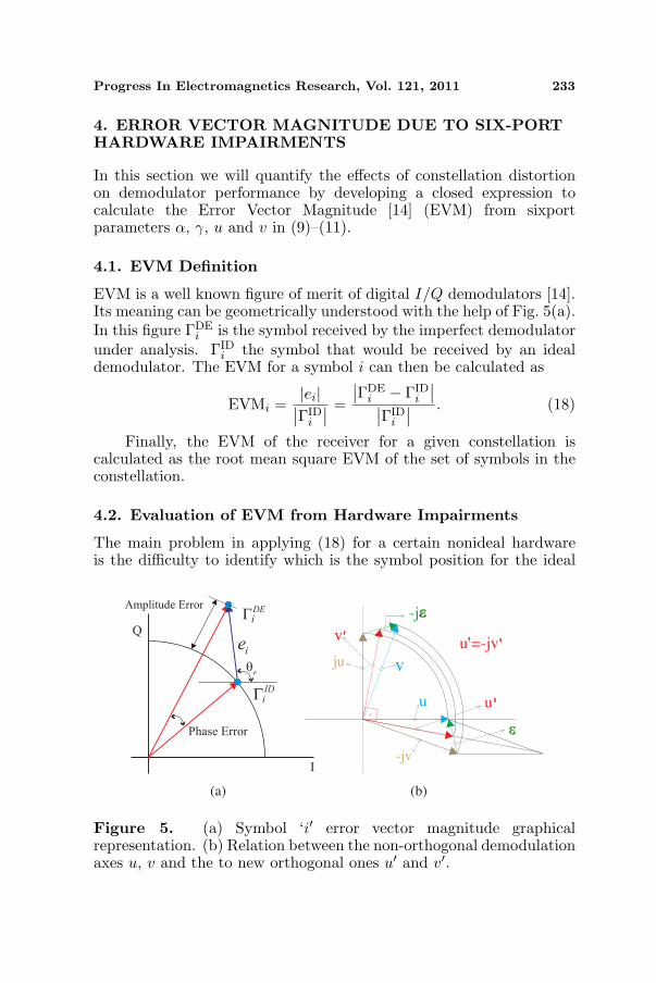
4.1. EVM Definition
EVM is a well known figure of merit of digital I/Q demodulators [14].Its meaning can be geometrically understood with the help of Fig. 5(a).In this figure ΓDE
i is the symbol received by the imperfect demodulatorunder analysis. ΓID
i the symbol that would be received by an idealdemodulator. The EVM for a symbol i can then be calculated as
EVMi =|ei|∣∣ΓID
i
∣∣ =
∣∣ΓDEi − ΓID
i
∣∣∣∣ΓID
i
∣∣ . (18)
Finally, the EVM of the receiver for a given constellation iscalculated as the root mean square EVM of the set of symbols in theconstellation.
4.2. Evaluation of EVM from Hardware Impairments
The main problem in applying (18) for a certain nonideal hardwareis the difficulty to identify which is the symbol position for the ideal
v
u
u =-jv
-j
u
vju
-jv
(a) (b)
ε
ε
'
' ''
Figure 5. (a) Symbol ‘i′ error vector magnitude graphicalrepresentation. (b) Relation between the non-orthogonal demodulationaxes u, v and the to new orthogonal ones u′ and v′.
234 Moscoso-Martir, Molina-Fernandez, and Ortega-Monux
demodulator: as argued in Section 2.1, there is an arbitrary constant,(U , see (4)), to be set whose amplitude and phase is related withreceiver Automatic Gain Control and Carrier Recovery Subsystem,respectively).
Let’s start with the complete receiver equation including allpossible impairments (α 6= 0, γ 6= 0, u 6= −jv) which we repeat herefor convenience
ΓDE = α + γ∣∣ΓRX
∣∣2 +{Re
(u∗ΓRX
)+ jRe
(v∗ΓRX
)}. (19)
The term in brackets of this equation can be interpreted as beingthe projections of ΓRX on the u and v axes respectively. As in a realsituation u and v will not fulfill the ideal orthogonality relation wecan define two ideal demodulation axes u′ and v′ fulfilling the idealcondition v′ = ju′ and being as close as possible to original ones. Thiscan be achieved by defining
u′ = u−jv2
v′ = ju′ = v+ju2
. (20)
The situation can be understood with the help of Fig. 5(b),where the relation between the different vectors can be graphicallyinterpreted. In this figure we have also depicted the new variable εdefined as
ε = u + jv, (21)
which is a measure of demodulation axis imbalance.From (20) and (21) we can write
u = u′ + ε2
v = ju′ − j ε2
, (22)
and substituting this into (19) and after some algebra we get
ΓDE = α + γ∣∣ΓRX
∣∣2 +(u′
)∗ ΓRX +ε
2(ΓRX
)∗. (23)
In this equation the term (u′)∗ ΓRX is easily recognized to be theideal demodulator symbol position (see (14)), i.e.,
ΓID =(u′
)∗ ΓRX, (24)
so the absolute Error Vector can be easily calculated for any symbol ias
ei = ΓDEi − ΓID
i = α + γ∣∣ΓRX
i
∣∣2 +ε
2(ΓRX
i
)∗(25)
and the EVM can be calculated for symbol i as
EVMi =
∣∣∣∣∣α
|u′|∣∣ΓRX
i
∣∣−1+
γ
|u′|∣∣ΓRX
i
∣∣ +ε
2 |u′|
(ΓRX
i
)∗∣∣ΓRX
i
∣∣
∣∣∣∣∣ . (26)
Progress In Electromagnetics Research, Vol. 121, 2011 235
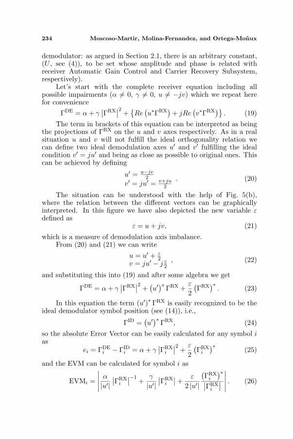
This equation is one of the main contributions of this paper asit allows to easily calculate the receiver performance degradation asthe vectorial sum of three different contributions. Hence, the followingcomplex numbers can be defined:
• DC rejectionRDC =
α
|u′| (27)
• Rectified Wave Rejection
RRW =γ
|u′| (28)
• Axis ImbalanceIA =
ε
2 |u′| =u + jv
2 |u′| (29)
These three complex numbers completely describe the perfor-mance degradation of the demodulator due to hardware impairmentsand their amplitudes are good figures of merit of demodulator’s per-formance. Notice that in (26) the three terms add vectorially to givethe total symbol EVM. Their influence depends on the received symbolamplitude
∣∣ΓRXi
∣∣ that in turn depends on the square root of the symbolto LO power ratio as seen in (15).
The worst case scenario occurs with all three terms adding inphase, which allows us to put an upper bound for symbol EVMi as
EVMMAX,i =|RDC|∣∣ΓRX
i
∣∣ 12
+ |RRW|∣∣ΓRX
i
∣∣ 12 + |IA| . (30)
Figure 6(a) shows this symbol EVM upper bound as a funcionof symbol to LO power. It can be clearly observed that DC rejectiondominates for low power symbols, rectified wave rejection dominatesfor high power symbols, and axis imbalance has a constant influence.Furthermore, an optimum point exists when
∣∣ΓRXi
∣∣2 =PRX,i
PLO=
∣∣∣∣α
γ
∣∣∣∣ , (31)
which minimizes hardware impairment degradation.However, it is well known that in these sixport receivers improved
performance is obtained for low PRX/PLO ratios [10, 11], so theyare tipically operated at PRX/PLO around −30 dB. This behavior iscontradictory with (31) and can only be explained if we take intoaccount that in these cases DC signal is removed using calibrationtechniques, so the effect of RDC is corrected by calibration. In fact, ifRDC = 0, (30) also predicts a better performance for lower PRX/PLO
236 Moscoso-Martir, Molina-Fernandez, and Ortega-Monux
-20 -10 0 10 200
5
10
15
20
25
30
PRX
/PLO
(dB)
EVMMAX,i
|RDC
||RX
|-1
|RRW
|| RX |
|IA|
-20 -10 0 10 200
5
10
15
20
25
30
PRX
/PLO
(dB)
EVMMAX,i
|RRW
|| RX|
|IA|
,'
(a) (b)
EV
M (
a.u
.)
EV
M (
a.u
.)
ΓΓ
Γ α
γ
γ
µ( )
Figure 6. Symbol EVM upper bound as a function of symbol toLO power and the effects of the three different contributions of (30).(a) Including RDC. (b) Removing RDC.
ratios, as shown in Fig. 6(b). Now, the effect of the rectified waverejection can be reduced increasing the LO power, so EVM tends toIA, which stablishes the minimum EVM of a specific receiver. Theminimum symbol to LO power ratio will be fixed by power detectorssince: i) a minimum RF power signal is needed to be detectable, andii) higher order nonlinearities limit the maximum LO power. In thefollowing sections it will be assumed that calibration removes DC signalterm (i.e., RDC = 0).
5. ERROR PROBABILITY DUE TO HARDWAREIMPAIRMENTS
The errors in symbol reception due to hardware impairments increasethe error probability. Hence, both of them must be related to set thereceiver hardware specifications from error probability and signal-to-noise ratio (SNR) specifications.
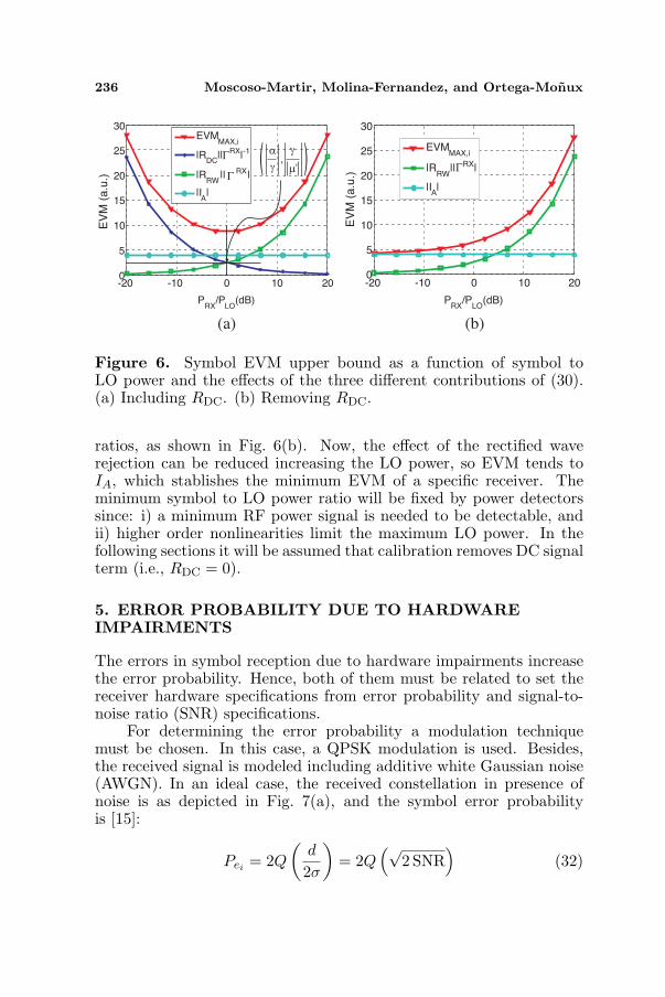
For determining the error probability a modulation techniquemust be chosen. In this case, a QPSK modulation is used. Besides,the received signal is modeled including additive white Gaussian noise(AWGN). In an ideal case, the received constellation in presence ofnoise is as depicted in Fig. 7(a), and the symbol error probabilityis [15]:
Pei = 2Q
(d
2σ
)= 2Q
(√2 SNR
)(32)
Progress In Electromagnetics Research, Vol. 121, 2011 237
2d
2d
2
d
2d
2d
2d
2d
2d
2
de
,2 Q i
de
(a) (b)
+
+
I,i
Figure 7. Received QPSK constellation. (a) In an ideal receiver.(b) In a real receiver.
Due to hardware impairments, signal and noise will suffer adistortion as predicted by (12). However, for small hardwareimpairments, typically required to assure a low BER, it can be assumedthat constellation distortion mostly affects the symbol positions butnot the noise gaussian distribution. This basic idea is illustratedin Fig. 7(b) where it is shown that symbol position is modified byhardware impairments but the noise contributions are still consideredas two dimensional uncorrelated Gaussians. This assumption will beshown in Section 6 to be correct for small hardware impairments andlow symbol to LO power ratios. The translation suffered by everysymbol can be calculated u sing (25). Thus, the error probability of areceived symbol is
Pei = Q
(√2 SNR +
Re (ei)σ
)+ Q
(√2 SNR +
Im (ei)σ
), (33)
and substituting σ using the SNR formula in a QPSK modulation [15]the symbol error probability can be rewritten as:
Pei =Q
(√2SNR+
Re(ei)√
4SNR∣∣ΓRXi
∣∣
)+Q
(√2SNR+
Im(ei)√
4SNR∣∣ΓRXi
∣∣
)(34)
Equation (34) is very significant as it allows to determine the errorprobability of each symbol relating it to the Error Vector shown in (25).In order to get an easier formulation, (34) is approximated by a secondorder Taylor series, so the error probability can be calculated from theSNR and the EVM (see Appendix A). Furthermore, since all QPSKsymbols have the same energy, and probability, the EVMi of all symbolwill be similar. In this case, assuming the worst case scenario and a
238 Moscoso-Martir, Molina-Fernandez, and Ortega-Monux
2 0 2 4 6 8 10 12 1410
10
10 5
100
SNR (dB)
BE
R u
pp
er
bo
un
d
EVM=0 %
EVM=6 %
EVM=12 %
EVM=18 %
-
-
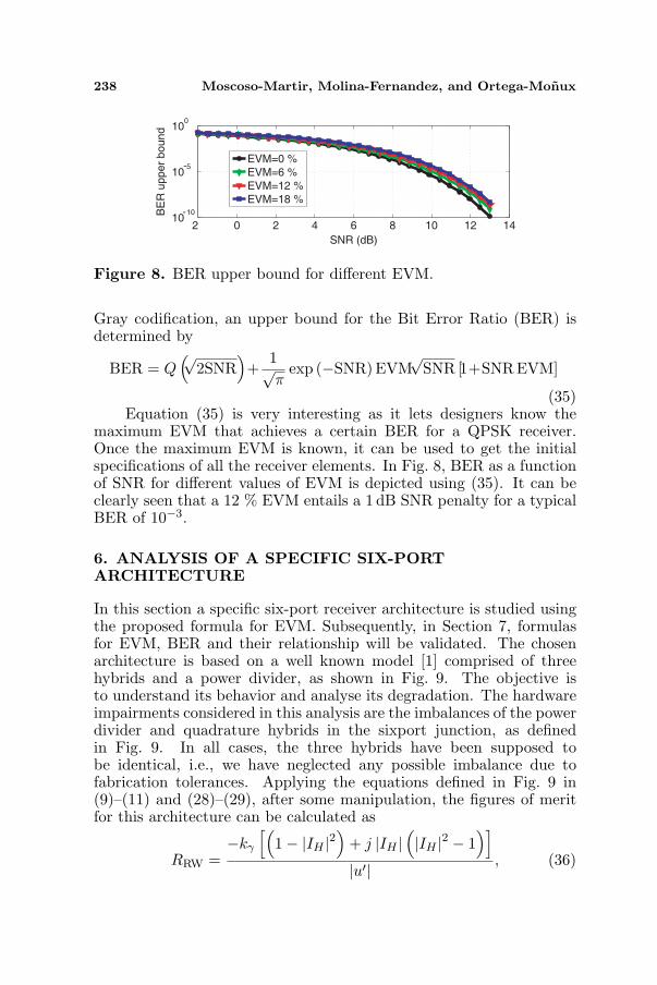
Figure 8. BER upper bound for different EVM.
Gray codification, an upper bound for the Bit Error Ratio (BER) isdetermined by
BER = Q(√
2SNR)+
1√π
exp (−SNR)EVM√
SNR [1+SNR EVM]
(35)Equation (35) is very interesting as it lets designers know the
maximum EVM that achieves a certain BER for a QPSK receiver.Once the maximum EVM is known, it can be used to get the initialspecifications of all the receiver elements. In Fig. 8, BER as a functionof SNR for different values of EVM is depicted using (35). It can beclearly seen that a 12 % EVM entails a 1 dB SNR penalty for a typicalBER of 10−3.
6. ANALYSIS OF A SPECIFIC SIX-PORTARCHITECTURE
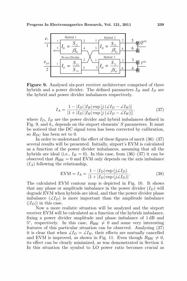
In this section a specific six-port receiver architecture is studied usingthe proposed formula for EVM. Subsequently, in Section 7, formulasfor EVM, BER and their relationship will be validated. The chosenarchitecture is based on a well known model [1] comprised of threehybrids and a power divider, as shown in Fig. 9. The objective isto understand its behavior and analyse its degradation. The hardwareimpairments considered in this analysis are the imbalances of the powerdivider and quadrature hybrids in the sixport junction, as definedin Fig. 9. In all cases, the three hybrids have been supposed tobe identical, i.e., we have neglected any possible imbalance due tofabrication tolerances. Applying the equations defined in Fig. 9 in(9)–(11) and (28)–(29), after some manipulation, the figures of meritfor this architecture can be calculated as
RRW =−kγ
[(1− |IH |2
)+ j |IH |
(|IH |2 − 1
)]
|u′| , (36)
Progress In Electromagnetics Research, Vol. 121, 2011 239
1
Hybrid 3
Hybrid 2
Po wer Divider
Hybrid 1
2
3
4
6
5
LOe
reDEQ
DEI
1 1
1
2
1
2
4
434
3 3
321
41
H
SI
jS
21
31
D
SI
S
21
41
H
SI
jS
21
41
H
SI
jS
2 2
=
=
=
=
Figure 9. Analysed six-port receiver architecture comprised of threehybrids and a power divider. The defined parameters IH and ID arethe hybrid and power divider imbalances respectively.
IA =1− |ID| |IH | exp [j (]ID − ]IH)]|1 + |ID| |IH | exp [j (]ID − ]IH)]| . (37)
where ID, IH are the power divider and hybrid imbalances defined inFig. 9, and kγ depends on the sixport elements’ S parameters. It mustbe noticed that the DC signal term has been corrected by calibration,so RDC has been set to 0.
In order to understand the effect of these figures of merit (36)–(37)several results will be presented. Initially, sixport’s EVM is calculatedas a function of the power divider imbalances, assuming that all thehybrids are ideal (i.e., IH = 0). In this case, from (36)–(37) it can beobserved that RRW = 0 and EVM only depends on the axis imbalance(IA) following the relationship,
EVM = IA =1− |ID| exp (j]ID)|1 + |ID| exp (j]ID)| . (38)
The calculated EVM contour map is depicted in Fig. 10. It showsthat any phase or amplitude imbalance in the power divider (ID) willdegrade EVM when hybrids are ideal, and that the power divider phaseimbalance (]ID) is more important than the amplitude imbalance(|ID|) in this case.
Now a more realistic situation will be analyzed and the sixportreceiver EVM will be calculated as a function of the hybrids imbalance,fixing a power divider amplitude and phase imbalance of 1 dB and5◦, respectively. In this case, RRW 6= 0 and some very interestingfeatures of this particular situation can be observed. Analysing (37)it is clear that when ]ID = ]IH , their effects are mutually cancelledand EVM is improved, as shown in Fig. 11. Even though RRW 6= 0,its effect can be clearly minimized, as was demonstrated in Section 4.In this situation the symbol to LO power ratio becomes crucial as
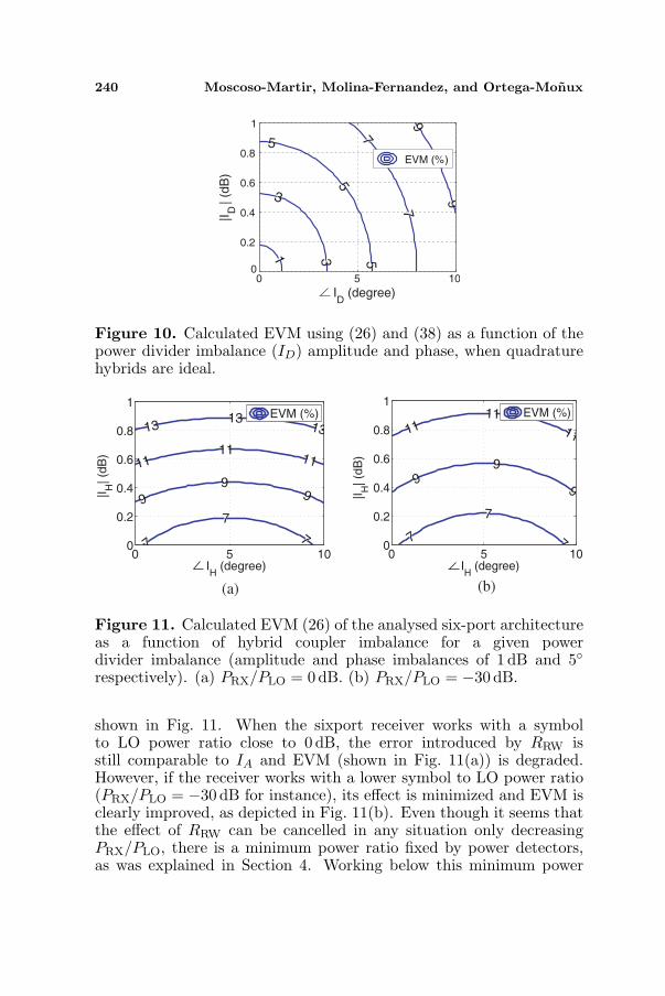
240 Moscoso-Martir, Molina-Fernandez, and Ortega-Monux
1 3
3
5
5
5 7
79
9
ID
(degree)
|ID
| (d
B)
0 5 100
0.2
0.4
0.6
0.8
1
EVM (%)
Figure 10. Calculated EVM using (26) and (38) as a function of thepower divider imbalance (ID) amplitude and phase, when quadraturehybrids are ideal.
7
7
7
9
99
1111
11
1313
13
IH
(degree)
|IH
| (d
B)
0 5 100
0.2
0.4
0.6
0.8
1EVM (%)
7
7
7
99
9
1111()
11
IH
(degree)
|IH
| (d
B)
0 5 100
0.2
0.4
0.6
0.8
1EVM (%)
(a) (b)
Figure 11. Calculated EVM (26) of the analysed six-port architectureas a function of hybrid coupler imbalance for a given powerdivider imbalance (amplitude and phase imbalances of 1 dB and 5◦respectively). (a) PRX/PLO = 0 dB. (b) PRX/PLO = −30 dB.
shown in Fig. 11. When the sixport receiver works with a symbolto LO power ratio close to 0 dB, the error introduced by RRW isstill comparable to IA and EVM (shown in Fig. 11(a)) is degraded.However, if the receiver works with a lower symbol to LO power ratio(PRX/PLO = −30 dB for instance), its effect is minimized and EVM isclearly improved, as depicted in Fig. 11(b). Even though it seems thatthe effect of RRW can be cancelled in any situation only decreasingPRX/PLO, there is a minimum power ratio fixed by power detectors,as was explained in Section 4. Working below this minimum power
Progress In Electromagnetics Research, Vol. 121, 2011 241
ratio, power detectors (not considered in our analysis) will degradeEVM. Hence, the optimum operation point will depend on the specificsixport receiver realization.
The analysis performed in this section has shown the importanceof EVM Equation (26) and its three figures of merit (RDC, RRW andIA). They can be used to obtain simple formulas for any sixportarchitecture as (36)–(37) that allow to get a deeper insight into itsbehavior and even determine the component requirements.
7. VALIDATION OF THE PROPOSED FORMULAS
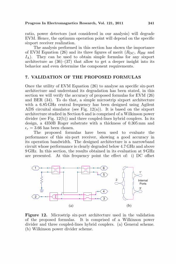
Once the utility of EVM Equation (26) to analyse an specific six-portarchitecture and understand its degradation has been stated, in thissection we will verify the accuracy of proposed formulas for EVM (26)and BER (34). To do that, a simple microstrip sixport architecturewith a 6.85 GHz central frequency has been designed using AgilentADS circuital simulator (see Fig. 12(a)). It is based on the sixportarchitecture studied in Section 6 and is comprised of a Wilkinson powerdivider (see Fig. 12(b)) and three coupled-lines hybrid couplers. In itsdesign, a 4350B Roger substrate with a thickness of 0.305mm andεr = 3.66 has been chosen.
The proposed formulas have been used to evaluate theperformance of this six-port receiver, showing a good accuracy inits operation bandwidth. The designed architecture is a narrowbandcircuit whose performance is clearly degraded below 4.7GHz and above9GHz. In this section, the results obtained in its evaluation at 9GHzare presented. At this frequency point the effect of: i) DC offset
2
1 6
5
4
3
2
3’
1’
Internal
Ports
(a) (b)
Figure 12. Microstrip six-port architecture used in the validationof the proposed formulas. It is comprised of a Wilkinson powerdivider and three coupled-lines hybrid couplers. (a) General scheme.(b) Wilkinson power divider scheme.
242 Moscoso-Martir, Molina-Fernandez, and Ortega-Monux
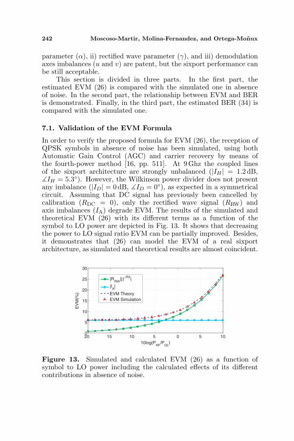
parameter (α), ii) rectified wave parameter (γ), and iii) demodulationaxes imbalances (u and v) are patent, but the sixport performance canbe still acceptable.
This section is divided in three parts. In the first part, theestimated EVM (26) is compared with the simulated one in absenceof noise. In the second part, the relationship between EVM and BERis demonstrated. Finally, in the third part, the estimated BER (34) iscompared with the simulated one.
7.1. Validation of the EVM Formula
In order to verify the proposed formula for EVM (26), the reception ofQPSK symbols in absence of noise has been simulated, using bothAutomatic Gain Control (AGC) and carrier recovery by means ofthe fourth-power method [16, pp. 511]. At 9Ghz the coupled linesof the sixport architecture are strongly unbalanced (|IH | = 1.2 dB,]IH = 5.3◦). However, the Wilkinson power divider does not presentany imbalance (|ID| = 0 dB, ]ID = 0◦), as expected in a symmetricalcircuit. Assuming that DC signal has previously been cancelled bycalibration (RDC = 0), only the rectified wave signal (RRW) andaxis imbalances (IA) degrade EVM. The results of the simulated andtheoretical EVM (26) with its different terms as a function of thesymbol to LO power are depicted in Fig. 13. It shows that decreasingthe power to LO signal ratio EVM can be partially improved. Besides,it demonstrates that (26) can model the EVM of a real sixportarchitecture, as simulated and theoretical results are almost coincident.
20 15 10 5 0 5 100
5
10
15
20
25
30
10log(PRF
/POL
)
EV
M(%
)
|RRW
||ΓRX|
|IA|
EVM Theory
EVM Simulation
Figure 13. Simulated and calculated EVM (26) as a function ofsymbol to LO power including the calculated effects of its differentcontributions in absence of noise.
Progress In Electromagnetics Research, Vol. 121, 2011 243
-20 -15 -10 -5 0 5 10
-8
-6
-4
-2
PRX /P LO (dB)
BE
R
SNR=8 dB
SNR=10 dB
SNR=12 dB
10
10
10
10
Figure 14. Simulated BER as a function symbol to LO power ratiofor different SNR using the designed sixport architecture at 9 GHz.
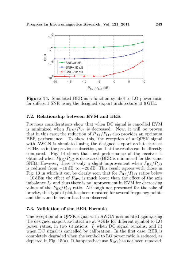
7.2. Relationship between EVM and BER
Previous considerations show that when DC signal is cancelled EVMis minimized when PRX/PLO is decreased. Now, it will be proventhat in this case, the reduction of PRX/PLO also provides an optimumBER performance. To show this, the reception of a QPSK signalwith AWGN is simulated using the designed sixport architecture at9GHz, as in the previous subsection, so that the results can be directlycompared. Fig. 14 shows that best performance of the receiver isobtained when PRX/PLO is decreased (BER is minimized for the sameSNR). However, there is only a slight improvement when PRX/PLO
is reduced from −10 dB to −20 dB. This result agrees with those inFig. 13 in which it can be clearly seen that for PRX/PLO ratios below−10 dBm the effect of RRW is much lower than the effect of the axisimbalance IA and thus there is no improvement in EVM for decreasingvalues of the PRX/PLO ratio. Although not presented for the sake ofbrevity, this type of plot has been repeated for several frequency pointsand the same behavior has been observed.
7.3. Validation of the BER Formula
The reception of a QPSK signal with AWGN is simulated again,usingthe designed sixport architecture at 9 GHz for different symbol to LOpower ratios, in two situations: i) when DC signal remains, and ii)when DC signal is cancelled by calibration. In the first case, BER iscompletely degraded when the symbol to LO power ratio is reduced, asdepicted in Fig. 15(a). It happens because RDC has not been removed,
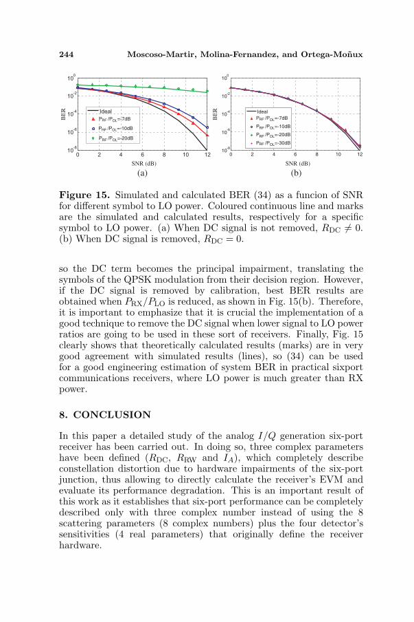
244 Moscoso-Martir, Molina-Fernandez, and Ortega-Monux
0 2 4 6 8 10 1210
-8
10-6
10-4
10-2
100
Ideal
PRF /POL=-7dB
PRF /POL=-10dB
PRF /POL=-20dB
PRF /POL=-30dB
(a) (b)
PRF /POL=-7dB
PRF /POL=-10dB
PRF /POL=-20dB
Figure 15. Simulated and calculated BER (34) as a funcion of SNRfor different symbol to LO power. Coloured continuous line and marksare the simulated and calculated results, respectively for a specificsymbol to LO power. (a) When DC signal is not removed, RDC 6= 0.(b) When DC signal is removed, RDC = 0.
so the DC term becomes the principal impairment, translating thesymbols of the QPSK modulation from their decision region. However,if the DC signal is removed by calibration, best BER results areobtained when PRX/PLO is reduced, as shown in Fig. 15(b). Therefore,it is important to emphasize that it is crucial the implementation of agood technique to remove the DC signal when lower signal to LO powerratios are going to be used in these sort of receivers. Finally, Fig. 15clearly shows that theoretically calculated results (marks) are in verygood agreement with simulated results (lines), so (34) can be usedfor a good engineering estimation of system BER in practical sixportcommunications receivers, where LO power is much greater than RXpower.
8. CONCLUSION
In this paper a detailed study of the analog I/Q generation six-portreceiver has been carried out. In doing so, three complex parametershave been defined (RDC, RRW and IA), which completely describeconstellation distortion due to hardware impairments of the six-portjunction, thus allowing to directly calculate the receiver’s EVM andevaluate its performance degradation. This is an important result ofthis work as it establishes that six-port performance can be completelydescribed only with three complex number instead of using the 8scattering parameters (8 complex numbers) plus the four detector’ssensitivities (4 real parameters) that originally define the receiverhardware.
Progress In Electromagnetics Research, Vol. 121, 2011 245
Simplified approximate formulas have been also obtained whichallow to easily calculate BER degradation due to hardwareimpairments, from the previously defined parameters. These areinteresting closed expressions which easily allow to set sixport hardwarespecifications to fulfill certain BER requirements. Altough theformulas have been derived for QPSK modulation, they could be easilyextended to other modulation techniques.
A six-port receiver architecture comprised of three hybrids and apower divider have been analysed using the three complex parameters(RDC, RRW and IA) to get a deeper understanding of its behaviour.Finally, the assessment of the proposed expressions has been carriedout by comparing the theoretically predicted EVM and BER, underAWGN, with the simulated ones for a specific microstrip sixportarchitecture, as a function of the PRX/PLO ratio.
ACKNOWLEDGMENT
This work has been founded by Andalusian Regional Ministry ofScience, Innovation and Business under projects P09- TIC-5268,MUPHY and a FPDI scholarship (780008), by European Union underproject MIRTHE (FP7-257980) and by AT4wireless under the contract8.06/5.59.3165.
APPENDIX A. ERROR PROBABILITYAPPROXIMATION FOR QPSK MODULATION
The error probability of a received symbol as a consequence of hardwareimpairments is stated in (33) or (34). The Q function can be rewrittenusing a Taylor series with an infinite sum of terms, but in this case asecond degree polynomial has been used
Q (x) ≈ Q (x0) + Q′ (x0) (x− x0) +Q′′ (x0)
2(x− x0)
2 . (A1)
This approximation is valid for good performance receivers. Then,using (A1) in (33) and substituting
|ei|2σ2
=|ei|2∣∣ΓID
i
∣∣2∣∣ΓID
i
∣∣2σ2
= 4 SNREVM2i , (A2)
Re (ei) + Im (ei)σ
=√
4 SNR EVM2i (cos θei + sin θei) , (A3)
246 Moscoso-Martir, Molina-Fernandez, and Ortega-Monux
after some algebra the approximated symbol error probability can bededuced as
Pei = 2Q(√
2SNR)−
− 1√π
exp (−SNR)EVMi
√SNR
[√2 (cos θei+sin θei)−2SNREVMi
],(A4)
where θei is the vector error angle of the received symbol (see Fig. 5(a)).As evident from (A4), the symbol error probability depend on thesymbol position. Hence, the worst case can be assumed (θei = 225◦)to get an upper bound.
REFERENCES
1. Li, R., R. G. Bosisio, and K. Wu, “A six-port digitalmillimeter wave receiver,” IEEE MTT-S International MicrowaveSymposium Digest, 1994.
2. Tatu, S. O., E. Moldovan, K. Wu, and R. G. Bosisio, “A newdirect millimeter-wave six-port receiver,” IEEE Transactions onMicrowave Theory and Techniques, Vol. 49, No. 12, 2517–2522,Dec. 2001.
3. Mallat, K., E. Moldovan, and S. O. Tatu, “Comparativedemodulation results for six-port and conventional 60 GHz directconversion receivers,” Progress In Electromagnetics Research,Vol. 84, 437–449, 2008.
4. Perez-Duenas, J., J. G. Wangumert-Perez, and I. Molina-Fernandez, “Novel modulation scheme and six-port basedrake receiver for DS-UWB,” IEEE Transactions on WirelessCommunications, Vol. 8, No. 7, 3628–3633, Jul. 2009.
5. Seimetz, M. and C.-M. Weinert, “Options, feasibility, andavailability of 2 × 4 90◦ hybrids for coherent optical systems,”Journal of Lightwave Technology, Vol. 24, No. 3, 1317–1322,Mar. 2006.
6. Kunkel, R., H.-G. Bach, D. Hoffmann, C. M. Weinert, I. Molina-Fernandez, and R. Halir, “First monolithic InP-based 90◦-hybrid OEIC comprising balanced detectors for 100GE coherentfrontends,” IEEE International Conference on Indium Phosphide& Related Materials, May 2009.
7. “Implementation Agreement for Integrated Dual Polariza-tion Intradyne Coherent Receivers,” Optical InternetworkingForum, Apr. 2010. Available: http://www.oiforum.com/pu-blic/documents/OIF DPC RX-01.0.pdf.
Progress In Electromagnetics Research, Vol. 121, 2011 247
8. Perez-Lara, P., I. Molina-Fernandez, and J. G. Wangumert-Perez, “Effects of hardware imperfection on six-port direct digitalreceivers calibrated with three and four signal standards,” IEEProceedings Microwaves, Antennas and Propagation, Vol. 153,No. 2, 171–176, Apr. 2006.
9. Henstschel, T., “The six-port as a communications receiver,”IEEE Transactions on Microwave Theory and Techniques, Vol. 53,No. 3, 1039–1047, Mar. 2005.
10. Winter, S. M., H. J. Ehm, A. Koelpin, and R. Weigel, “Analysisof system parameters of a six-port communications receiver withanalog I/Q regeneration,” International Sympodium on Signal,Systems and Electronics, 375–378. Jul. 2007.
11. Winter, S. M., H. J. Ehm, A. Koelpin, and R. Weigel, “Diodepower detector dc operating point in six-port communications re-ceivers,” Proceedings of the 37th European Microwave Conference,795–798, Oct. 2007.
12. Engen, G. F., “The six-port reflectometer: An alternativenetwork analyzer,” IEEE Transactions on Microwave Theory andTechniques, Vol. 25, No. 12, 1075–1079, Dec. 1977.
13. Mailand, M., R. Richter, and H.-J. Jentschel, “Nonlinearityanalysis of power detectors in direct conversion receiversutilizing six-port technology,” International Symposium onSignals, Circuits and Systems, 123–126, Sep. 2005.
14. McKinley, M. D., K. A. Remley, M. Myslinski, J. S. Kenney,D. Schreurs, and B. Nauwelaers, “EVM calculation for broadbandmodulated signals,” Proceedings of the 64th ARFTG Conference,45–52, Dec. 2004.
15. Proakis, J. G., Digital Communications, 4th edition, MacGraw-Hill, Aug. 2000.
16. Jeruchim, M. C., P. Balaban, and K. S. Shanmugan, Simulation ofCommunication Systems Modelling Methodology, and Techniques,2nd edition, Kluwer Academic/Plenum Publishers, 2000.