si7006-a20 - silicon labs · precision relative humidity sensor ± 5% rh (max), 0–90% rh high...
TRANSCRIPT
Rev. 1.2 8/16 Copyright © 2016 by Silicon Laboratories Si7006-A20
Si7006-A20
I2C HUMIDITY AND TEMPERATURE SENSOR
Features
Applications
Description
The Si7006 I2C Humidity and Temperature Sensor is a monolithic CMOS ICintegrating humidity and temperature sensor elements, an analog-to-digitalconverter, signal processing, calibration data, and an I2C Interface. The patenteduse of industry-standard, low-K polymeric dielectrics for sensing humidity enablesthe construction of low-power, monolithic CMOS Sensor ICs with low drift andhysteresis, and excellent long term stability.
The humidity and temperature sensors are factory-calibrated and the calibrationdata is stored in the on-chip non-volatile memory. This ensures that the sensorsare fully interchangeable, with no recalibration or software changes required.
The Si7006 is available in a 3x3 mm DFN package and is reflow solderable. It canbe used as a hardware- and software-compatible drop-in upgrade for existing RH/temperature sensors in 3x3 mm DFN-6 packages, featuring precision sensingover a wider range and lower power consumption. The optional factory-installedcover offers a low profile, convenient means of protecting the sensor duringassembly (e.g., reflow soldering) and throughout the life of the product, excludingliquids (hydrophobic/oleophobic) and particulates.
The Si7006 offers an accurate, low-power, factory-calibrated digital solution idealfor measuring humidity, dew-point, and temperature, in applications ranging fromHVAC/R and asset tracking to industrial and consumer platforms.
Precision Relative Humidity Sensor ± 5% RH (max), 0–90% RH
High Accuracy Temperature Sensor±1 °C (max), –10 to 85 °C
0 to 100% RH operating range –40 to +125 °C operating range Wide operating voltage
(1.9 to 3.6 V) Low Power Consumption
150 µA active current60 nA standby current
Factory-calibrated
I2C Interface Integrated on-chip heater 3x3 mm DFN Package Excellent long term stability Optional factory-installed cover
Low-profileProtection during reflowExcludes liquids and particulates
HVAC/R Thermostats/humidistats Respiratory therapy White goods Indoor weather stations
Micro-environments/data centers Automotive climate control anddefogging Asset and goods tracking Mobile phones and tablets
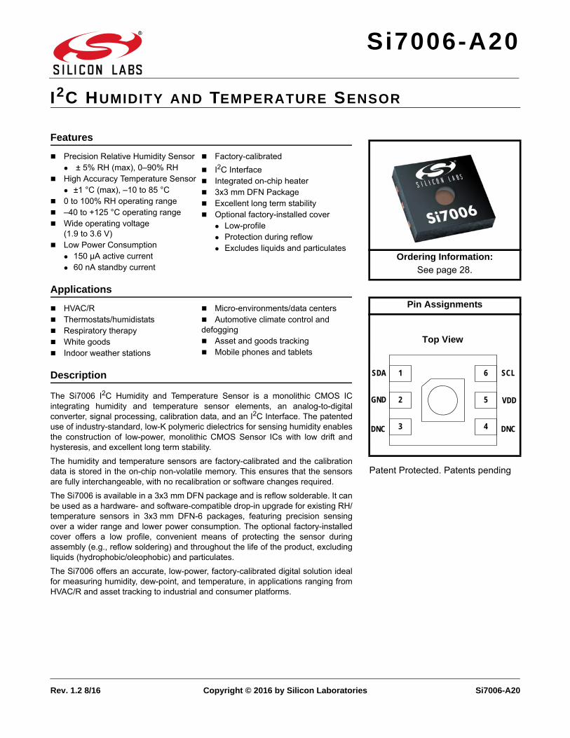
Patent Protected. Patents pending
Ordering Information:
See page 28.
Pin Assignments
DNC
SCL
VDD
1
2
6
5GND
SDA
3 4DNC
Top View
Si7006-A20
2 Rev. 1.2
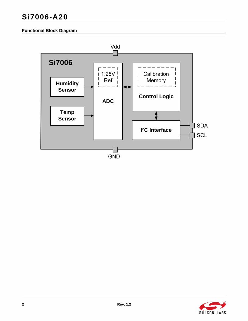
Functional Block Diagram
ADC
GND
Humidity Sensor
Control Logic
SCL
Si7006
Temp Sensor
1.25V Ref
I2C InterfaceSDA
Vdd
Calibration Memory
Si7006-A20
Rev. 1.2 3
TABLE OF CONTENTS
Section Page
1. Electrical Specifications . . . . . . . . . . . . . . . . . . . . . . . . . . . . . . . . . . . . . . . . . . . . . . . . . . .42. Typical Application Circuits . . . . . . . . . . . . . . . . . . . . . . . . . . . . . . . . . . . . . . . . . . . . . . .113. Bill of Materials . . . . . . . . . . . . . . . . . . . . . . . . . . . . . . . . . . . . . . . . . . . . . . . . . . . . . . . . . .124. Functional Description . . . . . . . . . . . . . . . . . . . . . . . . . . . . . . . . . . . . . . . . . . . . . . . . . . .13
4.1. Relative Humidity Sensor Accuracy . . . . . . . . . . . . . . . . . . . . . . . . . . . . . . . . . . . . .144.2. Hysteresis . . . . . . . . . . . . . . . . . . . . . . . . . . . . . . . . . . . . . . . . . . . . . . . . . . . . . . . . .154.3. Prolonged Exposure to High Humidity . . . . . . . . . . . . . . . . . . . . . . . . . . . . . . . . . . .154.4. PCB Assembly . . . . . . . . . . . . . . . . . . . . . . . . . . . . . . . . . . . . . . . . . . . . . . . . . . . . .154.5. Protecting the Sensor . . . . . . . . . . . . . . . . . . . . . . . . . . . . . . . . . . . . . . . . . . . . . . . .174.6. Bake/Hydrate Procedure . . . . . . . . . . . . . . . . . . . . . . . . . . . . . . . . . . . . . . . . . . . . . .174.7. Long Term Drift/Aging . . . . . . . . . . . . . . . . . . . . . . . . . . . . . . . . . . . . . . . . . . . . . . . .17
5. I2C Interface . . . . . . . . . . . . . . . . . . . . . . . . . . . . . . . . . . . . . . . . . . . . . . . . . . . . . . . . . . . .185.1. Issuing a Measurement Command . . . . . . . . . . . . . . . . . . . . . . . . . . . . . . . . . . . . . .195.2. Reading and Writing User Registers . . . . . . . . . . . . . . . . . . . . . . . . . . . . . . . . . . . . .225.3. Electronic Serial Number . . . . . . . . . . . . . . . . . . . . . . . . . . . . . . . . . . . . . . . . . . . . .235.4. Firmware Revision . . . . . . . . . . . . . . . . . . . . . . . . . . . . . . . . . . . . . . . . . . . . . . . . . .235.5. Heater . . . . . . . . . . . . . . . . . . . . . . . . . . . . . . . . . . . . . . . . . . . . . . . . . . . . . . . . . . . .24
6. Control Registers . . . . . . . . . . . . . . . . . . . . . . . . . . . . . . . . . . . . . . . . . . . . . . . . . . . . . . . .256.1. Register Descriptions . . . . . . . . . . . . . . . . . . . . . . . . . . . . . . . . . . . . . . . . . . . . . . . .25
7. Pin Descriptions: Si7006 (Top View) . . . . . . . . . . . . . . . . . . . . . . . . . . . . . . . . . . . . . . . .278. Ordering Guide . . . . . . . . . . . . . . . . . . . . . . . . . . . . . . . . . . . . . . . . . . . . . . . . . . . . . . . . . .289. Package Outline . . . . . . . . . . . . . . . . . . . . . . . . . . . . . . . . . . . . . . . . . . . . . . . . . . . . . . . . .29
9.1. Package Outline: 3x3 6-pin DFN . . . . . . . . . . . . . . . . . . . . . . . . . . . . . . . . . . . . . . . .299.2. Package Outline: 3x3 6-pin DFN with Protective Cover . . . . . . . . . . . . . . . . . . . . . .30
10. PCB Land Pattern and Solder Mask Design . . . . . . . . . . . . . . . . . . . . . . . . . . . . . . . . .3111. Top Marking . . . . . . . . . . . . . . . . . . . . . . . . . . . . . . . . . . . . . . . . . . . . . . . . . . . . . . . . . . .32
11.1. Si7006 Top Marking . . . . . . . . . . . . . . . . . . . . . . . . . . . . . . . . . . . . . . . . . . . . . . . .3211.2. Top Marking Explanation . . . . . . . . . . . . . . . . . . . . . . . . . . . . . . . . . . . . . . . . . . . .32
12. Additional Reference Resources . . . . . . . . . . . . . . . . . . . . . . . . . . . . . . . . . . . . . . . . . .33Document Change List . . . . . . . . . . . . . . . . . . . . . . . . . . . . . . . . . . . . . . . . . . . . . . . . . . . . .34
Si7006-A20
4 Rev. 1.2
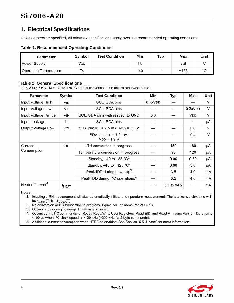
1. Electrical Specifications
Unless otherwise specified, all min/max specifications apply over the recommended operating conditions.
Table 1. Recommended Operating Conditions
Parameter Symbol Test Condition Min Typ Max Unit
Power Supply VDD 1.9 3.6 V
Operating Temperature TA –40 — +125 °C
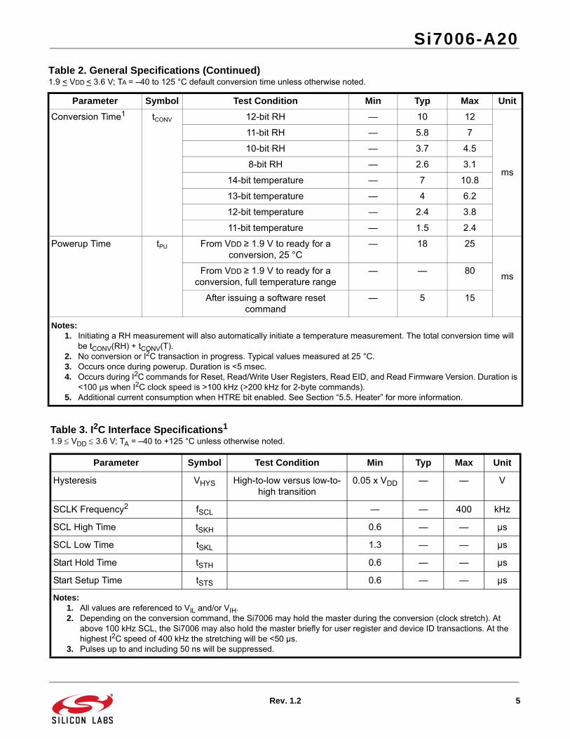
Table 2. General Specifications1.9 < VDD < 3.6 V; TA = –40 to 125 °C default conversion time unless otherwise noted.
Parameter Symbol Test Condition Min Typ Max Unit
Input Voltage High VIH SCL, SDA pins 0.7xVDD — — V
Input Voltage Low VIL SCL, SDA pins — — 0.3xVDD V
Input Voltage Range VIN SCL, SDA pins with respect to GND 0.0 — VDD V
Input Leakage IIL SCL, SDA pins — — 1 μA
Output Voltage Low VOL SDA pin; IOL = 2.5 mA; VDD = 3.3 V — — 0.6 V
SDA pin; IOL = 1.2 mA; VDD = 1.9 V
— — 0.4 V
Current Consumption
IDD RH conversion in progress — 150 180 μA
Temperature conversion in progress — 90 120 μA
Standby, –40 to +85 °C2 — 0.06 0.62 μA
Standby, –40 to +125 °C2 — 0.06 3.8 μA
Peak IDD during powerup3 — 3.5 4.0 mA
Peak IDD during I2C operations4 — 3.5 4.0 mA
Heater Current5 IHEAT — 3.1 to 94.2 — mA
Notes:1. Initiating a RH measurement will also automatically initiate a temperature measurement. The total conversion time will
be tCONV(RH) + tCONV(T).2. No conversion or I2C transaction in progress. Typical values measured at 25 °C.3. Occurs once during powerup. Duration is <5 msec.4. Occurs during I2C commands for Reset, Read/Write User Registers, Read EID, and Read Firmware Version. Duration is
<100 µs when I2C clock speed is >100 kHz (>200 kHz for 2-byte commands). 5. Additional current consumption when HTRE bit enabled. See Section “5.5. Heater” for more information.
Si7006-A20
Rev. 1.2 5
Conversion Time1 tCONV 12-bit RH — 10 12
ms
11-bit RH — 5.8 7
10-bit RH — 3.7 4.5
8-bit RH — 2.6 3.1
14-bit temperature — 7 10.8
13-bit temperature — 4 6.2
12-bit temperature — 2.4 3.8
11-bit temperature — 1.5 2.4
Powerup Time tPU From VDD ≥ 1.9 V to ready for a conversion, 25 °C
— 18 25
msFrom VDD ≥ 1.9 V to ready for a
conversion, full temperature range— — 80
After issuing a software resetcommand
— 5 15
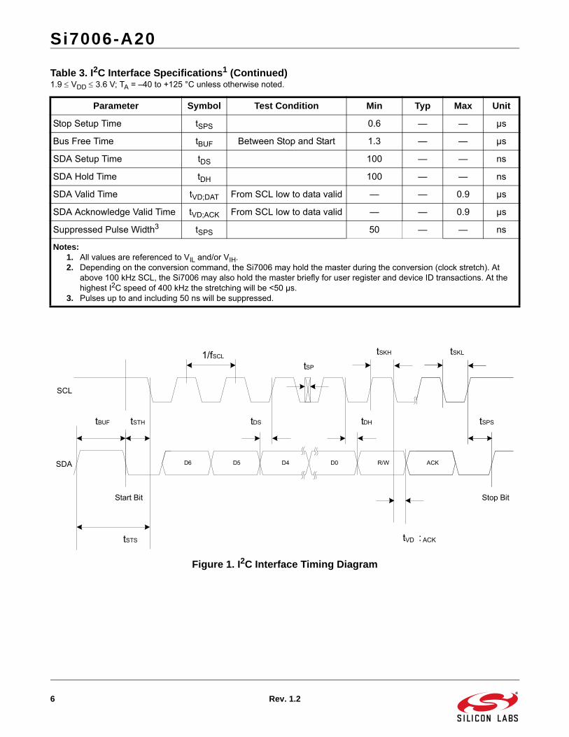
Table 3. I2C Interface Specifications1
1.9 VDD 3.6 V; TA = –40 to +125 °C unless otherwise noted.
Parameter Symbol Test Condition Min Typ Max Unit
Hysteresis VHYS High-to-low versus low-to-high transition
0.05 x VDD — — V
SCLK Frequency2 fSCL — — 400 kHz
SCL High Time tSKH 0.6 — — µs
SCL Low Time tSKL 1.3 — — µs
Start Hold Time tSTH 0.6 — — µs
Start Setup Time tSTS 0.6 — — µs
Notes:1. All values are referenced to VIL and/or VIH.2. Depending on the conversion command, the Si7006 may hold the master during the conversion (clock stretch). At
above 100 kHz SCL, the Si7006 may also hold the master briefly for user register and device ID transactions. At the highest I2C speed of 400 kHz the stretching will be <50 µs.
3. Pulses up to and including 50 ns will be suppressed.
Table 2. General Specifications (Continued)1.9 < VDD < 3.6 V; TA = –40 to 125 °C default conversion time unless otherwise noted.
Parameter Symbol Test Condition Min Typ Max Unit
Notes:1. Initiating a RH measurement will also automatically initiate a temperature measurement. The total conversion time will
be tCONV(RH) + tCONV(T).2. No conversion or I2C transaction in progress. Typical values measured at 25 °C.3. Occurs once during powerup. Duration is <5 msec.4. Occurs during I2C commands for Reset, Read/Write User Registers, Read EID, and Read Firmware Version. Duration is
<100 µs when I2C clock speed is >100 kHz (>200 kHz for 2-byte commands). 5. Additional current consumption when HTRE bit enabled. See Section “5.5. Heater” for more information.
Si7006-A20
6 Rev. 1.2
Figure 1. I2C Interface Timing Diagram
Stop Setup Time tSPS 0.6 — — µs
Bus Free Time tBUF Between Stop and Start 1.3 — — µs
SDA Setup Time tDS 100 — — ns
SDA Hold Time tDH 100 — — ns
SDA Valid Time tVD;DAT From SCL low to data valid — — 0.9 µs
SDA Acknowledge Valid Time tVD;ACK From SCL low to data valid — — 0.9 µs
Suppressed Pulse Width3 tSPS 50 — — ns
Table 3. I2C Interface Specifications1 (Continued)1.9 VDD 3.6 V; TA = –40 to +125 °C unless otherwise noted.
Parameter Symbol Test Condition Min Typ Max Unit
Notes:1. All values are referenced to VIL and/or VIH.2. Depending on the conversion command, the Si7006 may hold the master during the conversion (clock stretch). At
above 100 kHz SCL, the Si7006 may also hold the master briefly for user register and device ID transactions. At the highest I2C speed of 400 kHz the stretching will be <50 µs.
3. Pulses up to and including 50 ns will be suppressed.
SCL
D6
1/fSCLtSKH
SDA
tSKL
tSTH
D5 D4 D0 R/W ACK
tDS tDH
Start Bit Stop Bit
tBUF
tSTS tVD : ACK
tSPS
tSP
Si7006-A20
Rev. 1.2 7
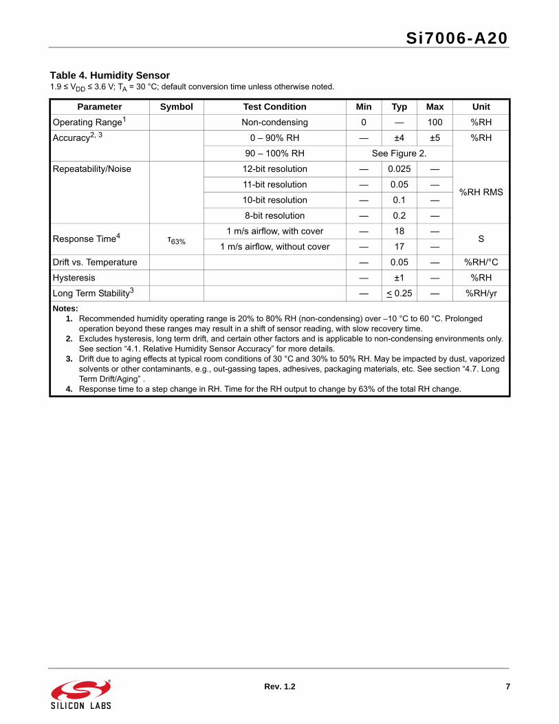
Table 4. Humidity Sensor1.9 ≤ VDD ≤ 3.6 V; TA = 30 °C; default conversion time unless otherwise noted.
Parameter Symbol Test Condition Min Typ Max Unit
Operating Range1 Non-condensing 0 — 100 %RH
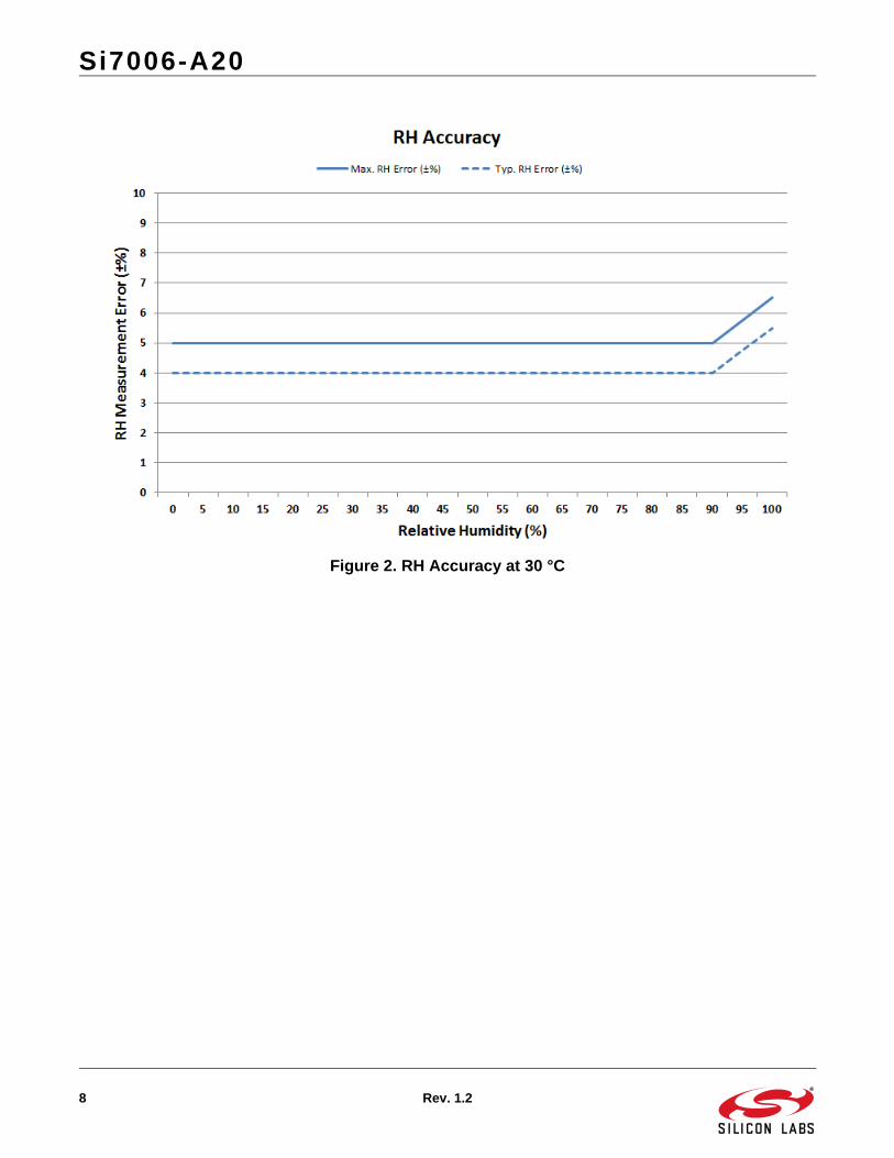
Accuracy2, 3 0 – 90% RH — ±4 ±5 %RH
90 – 100% RH See Figure 2.
Repeatability/Noise 12-bit resolution — 0.025 —
%RH RMS11-bit resolution — 0.05 —
10-bit resolution — 0.1 —
8-bit resolution — 0.2 —
Response Time4 τ63%1 m/s airflow, with cover — 18 —
S1 m/s airflow, without cover — 17 —
Drift vs. Temperature — 0.05 — %RH/°C
Hysteresis — ±1 — %RH
Long Term Stability3 — < 0.25 — %RH/yr
Notes:1. Recommended humidity operating range is 20% to 80% RH (non-condensing) over –10 °C to 60 °C. Prolonged
operation beyond these ranges may result in a shift of sensor reading, with slow recovery time.2. Excludes hysteresis, long term drift, and certain other factors and is applicable to non-condensing environments only.
See section “4.1. Relative Humidity Sensor Accuracy” for more details.3. Drift due to aging effects at typical room conditions of 30 °C and 30% to 50% RH. May be impacted by dust, vaporized
solvents or other contaminants, e.g., out-gassing tapes, adhesives, packaging materials, etc. See section “4.7. Long Term Drift/Aging” .
4. Response time to a step change in RH. Time for the RH output to change by 63% of the total RH change.
Si7006-A20
8 Rev. 1.2
Figure 2. RH Accuracy at 30 °C
Si7006-A20
Rev. 1.2 9
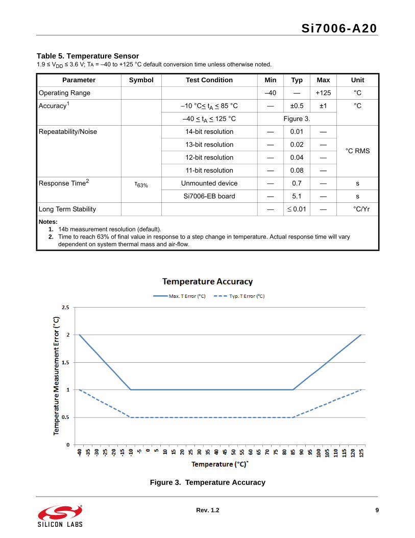
Figure 3. Temperature Accuracy
Table 5. Temperature Sensor1.9 ≤ VDD ≤ 3.6 V; TA = –40 to +125 °C default conversion time unless otherwise noted.
Parameter Symbol Test Condition Min Typ Max Unit
Operating Range –40 — +125 °C
Accuracy1 –10 °C< tA < 85 °C — ±0.5 ±1 °C
–40 < tA < 125 °C Figure 3.
Repeatability/Noise 14-bit resolution — 0.01 —
°C RMS13-bit resolution — 0.02 —
12-bit resolution — 0.04 —
11-bit resolution — 0.08 —
Response Time2 τ63% Unmounted device — 0.7 — s
Si7006-EB board — 5.1 — s
Long Term Stability — 0.01 — °C/Yr
Notes:1. 14b measurement resolution (default).2. Time to reach 63% of final value in response to a step change in temperature. Actual response time will vary
dependent on system thermal mass and air-flow.
Si7006-A20
10 Rev. 1.2
Table 6. Thermal Characteristics
Parameter Symbol Test Condition DFN-6 Unit
Junction to Air Thermal Resistance JA JEDEC 2-Layer board,No Airflow
256 °C/W
Junction to Air Thermal Resistance JA JEDEC 2-Layer board,1 m/s Airflow
224 °C/W
Junction to Air Thermal Resistance JA JEDEC 2-Layer board,2.5 m/s Airflow
205 °C/W
Junction to Case Thermal Resistance JC JEDEC 2-Layer board 22 °C/W
Junction to Board Thermal Resistance JB JEDEC 2-Layer board 134 °C/W
Table 7. Absolute Maximum Ratings1
Parameter Symbol Test Condition Min Typ Max Unit
Ambient temperature under bias
–55 — 125 °C
Storage Temperature2 –65 — 150 °C
Voltage on I/O pins –0.3 — VDD+0.3 V V
Voltage on VDD with respect to GND
–0.3 4.2 V
ESD Tolerance HBM — — 2 kV
CDM — — 1.25 kV
MM — — 250 V
Notes:1. Absolute maximum ratings are stress ratings only, operation at or beyond these conditions is not implied and may
shorten the life of the device or alter its performance.2. Special handling considerations apply; see application note, “AN607: Si70xx Humidity Sensor Designer’s Guide”.
Si7006-A20
Rev. 1.2 11
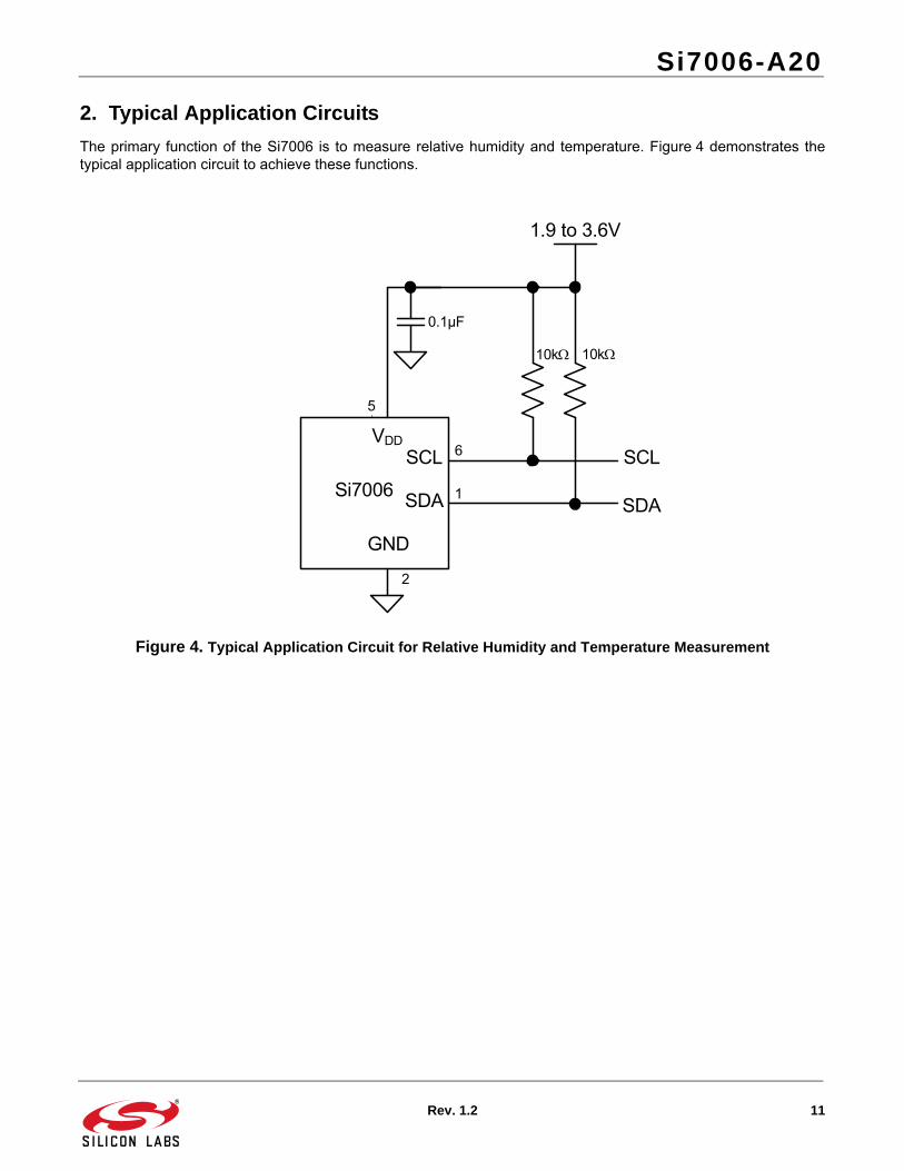
2. Typical Application Circuits
The primary function of the Si7006 is to measure relative humidity and temperature. Figure 4 demonstrates thetypical application circuit to achieve these functions.
Figure 4. Typical Application Circuit for Relative Humidity and Temperature Measurement
0.1µF
VDD
SCL
SDASi7006
SCL
SDA
1.9 to 3.6V
6
1
2
GND
10k10k
5
Si7006-A20
12 Rev. 1.2
3. Bill of Materials
Table 8. Typical Application Circuit BOM for Relative Humidity and Temperature Measurement
Reference Description Mfr Part Number Manufacturer
R1 Resistor, 10 k, ±5%, 1/16 W, 0603 CR0603-16W-103JT Venkel
R2 Resistor, 10 k, ±5%, 1/16 W, 0603 CR0603-16W-103JT Venkel
C1 Capacitor, 0.1 µF, 16 V, X7R, 0603 C0603X7R160-104M Venkel
U1 IC, Digital Temperature/humidity Sensor Si7006-A20-GM Silicon Labs
Si7006-A20
Rev. 1.2 13
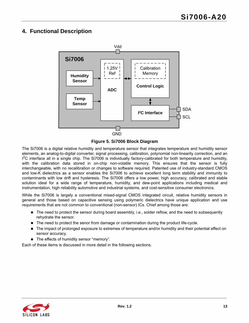
4. Functional Description
Figure 5. Si7006 Block Diagram
The Si7006 is a digital relative humidity and temperature sensor that integrates temperature and humidity sensorelements, an analog-to-digital converter, signal processing, calibration, polynomial non-linearity correction, and anI2C interface all in a single chip. The Si7006 is individually factory-calibrated for both temperature and humidity,with the calibration data stored in on-chip non-volatile memory. This ensures that the sensor is fullyinterchangeable, with no recalibration or changes to software required. Patented use of industry-standard CMOSand low-K dielectrics as a sensor enables the Si7006 to achieve excellent long term stability and immunity tocontaminants with low drift and hysteresis. The Si7006 offers a low power, high accuracy, calibrated and stablesolution ideal for a wide range of temperature, humidity, and dew-point applications including medical andinstrumentation, high reliability automotive and industrial systems, and cost-sensitive consumer electronics.
While the Si7006 is largely a conventional mixed-signal CMOS integrated circuit, relative humidity sensors ingeneral and those based on capacitive sensing using polymeric dielectrics have unique application and userequirements that are not common to conventional (non-sensor) ICs. Chief among those are:
The need to protect the sensor during board assembly, i.e., solder reflow, and the need to subsequently rehydrate the sensor.
The need to protect the senor from damage or contamination during the product life-cycle.
The impact of prolonged exposure to extremes of temperature and/or humidity and their potential effect on sensor accuracy.
The effects of humidity sensor “memory”.
Each of these items is discussed in more detail in the following sections.
ADC
GND
Humidity Sensor
Control Logic
SCL
Si7006
Temp Sensor
1.25V Ref
I2C InterfaceSDA
Vdd
Calibration Memory
Si7006-A20
14 Rev. 1.2
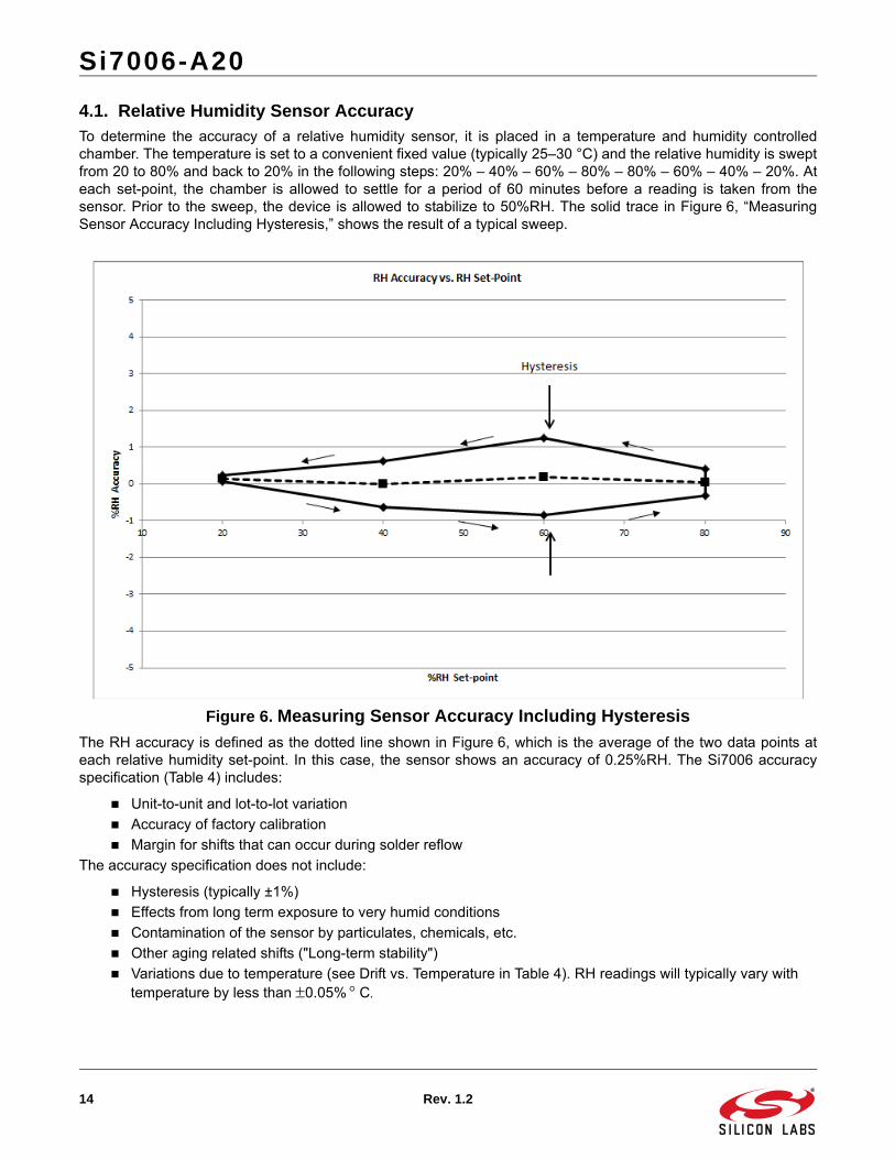
4.1. Relative Humidity Sensor AccuracyTo determine the accuracy of a relative humidity sensor, it is placed in a temperature and humidity controlledchamber. The temperature is set to a convenient fixed value (typically 25–30 °C) and the relative humidity is sweptfrom 20 to 80% and back to 20% in the following steps: 20% – 40% – 60% – 80% – 80% – 60% – 40% – 20%. Ateach set-point, the chamber is allowed to settle for a period of 60 minutes before a reading is taken from thesensor. Prior to the sweep, the device is allowed to stabilize to 50%RH. The solid trace in Figure 6, “MeasuringSensor Accuracy Including Hysteresis,” shows the result of a typical sweep.
Figure 6. Measuring Sensor Accuracy Including Hysteresis
The RH accuracy is defined as the dotted line shown in Figure 6, which is the average of the two data points ateach relative humidity set-point. In this case, the sensor shows an accuracy of 0.25%RH. The Si7006 accuracyspecification (Table 4) includes:
Unit-to-unit and lot-to-lot variation
Accuracy of factory calibration
Margin for shifts that can occur during solder reflow
The accuracy specification does not include:
Hysteresis (typically ±1%)
Effects from long term exposure to very humid conditions
Contamination of the sensor by particulates, chemicals, etc.
Other aging related shifts ("Long-term stability")
Variations due to temperature (see Drift vs. Temperature in Table 4). RH readings will typically vary with temperature by less than 0.05% C.
Si7006-A20
Rev. 1.2 15
4.2. HysteresisThe moisture absorbent film (polymeric dielectric) of the humidity sensor will carry a memory of its exposurehistory, particularly its recent or extreme exposure history. A sensor exposed to relatively low humidity will carry anegative offset relative to the factory calibration, and a sensor exposed to relatively high humidity will carry apositive offset relative to the factory calibration. This factor causes a hysteresis effect illustrated by the solid tracein Figure 6. The hysteresis value is the difference in %RH between the maximum absolute error on the decreasinghumidity ramp and the maximum absolute error on the increasing humidity ramp at a single relative humiditysetpoint and is expressed as a bipolar quantity relative to the average error (dashed trace). In the example ofFigure 6, the measurement uncertainty due to the hysteresis effect is ±1.0%RH.
4.3. Prolonged Exposure to High Humidity Prolonged exposure to high humidity will result in a gradual upward drift of the RH reading. The shift in sensorreading resulting from this drift will generally disappear slowly under normal ambient conditions. The amount ofshift is proportional to the magnitude of relative humidity and the length of exposure. In the case of lengthyexposure to high humidity, some of the resulting shift may persist indefinitely under typical conditions. It is generallypossible to substantially reverse this affect by baking the device (see Section “4.6. Bake/Hydrate Procedure” ).
4.4. PCB Assembly4.4.1. Soldering
Like most ICs, Si7006 devices are shipped from the factory vacuum-packed with an enclosed desiccant to avoidany RH accuracy drift during storage and to prevent any moisture-related issues during solder reflow. The followingguidelines should be observed during PCB assembly:
Si7006 devices are compatible with standard board assembly processes. Devices should be soldered using reflow per the recommended card reflow profile. See Section “10. PCB Land Pattern and Solder Mask Design” for the recommended card reflow profile.
A "no clean" solder process is recommended to minimize the need for water or solvent rinses after soldering. Cleaning after soldering is possible, but must be done carefully to avoid impacting the performance of the sensor. See “AN607: Si70xx Humidity Sensor Designer’s Guide” for more information on cleaning.
It is essential that the exposed polymer sensing film be kept clean and undamaged. This can be accomplished by careful handling and a clean, well-controlled assembly process. When in doubt or for extra protection, a heat-resistant, protective cover such as Kapton™ KPPD-1/8 polyimide tape can be installed during PCB assembly.
Si7006s may be ordered with a factory-fitted, solder-resistant protective cover. This cover provides protectionduring PCB assembly or rework but without the time and effort required to install and remove the Kapton tape. Itcan be left in place for the lifetime of the product, preventing liquids, dust or other contaminants from coming intocontact with the polymer sensor film. See Section “8. Ordering Guide” for a list of ordering part numbers thatinclude the cover.
4.4.2. Rehydration
The measured humidity value will generally shift slightly after solder reflow. A portion of this shift is permanent andis accounted for in the accuracy specifications in Table 4. After soldering, an Si7006 should be allowed toequilibrate under controlled RH conditions (room temperature, 45–55%RH) for at least 48 hours to eliminate theremainder of the shift and return the device to its specified accuracy performance.
Si7006-A20
16 Rev. 1.2
4.4.3. Rework
To maintain the specified sensor performance, care must be taken during rework to minimize the exposure of thedevice to excessive heat and to avoid damage/contamination or a shift in the sensor reading due to liquids, solderflux, etc. Manual touch-up using a soldering iron is permissible under the following guidelines:
The exposed polymer sensing film must be kept clean and undamaged. A protective cover is recommended during any rework operation (Kapton® tape or the factory installed cover).
Flux must not be allowed to contaminate the sensor; liquid flux is not recommended even with a cover in place. Conventional lead-free solder with rosin core is acceptable for touch-up as long as a cover is in place during the rework.
If possible, avoid water or solvent rinses after touch-up. Cleaning after soldering is possible, but must be done carefully to avoid impacting the performance of the sensor. See “AN607: Si70xx Humidity Sensor Designer’s Guide” for more information on cleaning.
Minimize the heating of the device. Soldering iron temperatures should not exceed 350 °C and the contact time per pin should not exceed five seconds.
Hot air rework is not recommended. If a device must be replaced, remove the device by hot air and solder a new part in its place by reflow following the guidelines above.
*Note: All trademarks are the property of their respective owners.
Figure 7. Si7006 with Factory-Installed Protective Cover
Si7006-A20
Rev. 1.2 17
4.5. Protecting the SensorBecause the sensor operates on the principal of measuring a change in capacitance, any changes to the dielectricconstant of the polymer film will be detected as a change in relative humidity. Therefore, it is important to minimizethe probability of contaminants coming into contact with the sensor. Dust and other particles as well as liquids canaffect the RH reading. It is recommended that a cover is employed in the end system that blocks contaminants butallows water vapor to pass through. Depending on the needs of the application, this can be as simple as plastic ormetallic gauze for basic protection against particulates or something more sophisticated such as a hydrophobicmembrane providing up to IP67 compliant protection.
The Si7006 may be ordered with a factory-fitted, solder-resistant cover that can be left in place for the lifetime ofthe product. It is very low-profile, hydrophobic and oleophobic. See Section “8. Ordering Guide” for a list of orderingpart numbers that include the cover. A dimensioned drawing of the IC with the cover is included in Section “9.Package Outline” . Other characteristics of the cover are listed in Table 9.
4.6. Bake/Hydrate ProcedureAfter exposure to extremes of temperature and/or humidity for prolonged periods, the polymer sensor film canbecome either very dry or very wet, in each case the result is either high or low relative humidity readings. Undernormal operating conditions, the induced error will diminish over time. From a very dry condition, such as aftershipment and soldering, the error will diminish over a few days at typical controlled ambient conditions, e.g.,48 hours of 45 ≤ %RH ≤ 55. However, from a very wet condition, recovery may take significantly longer. Toaccelerate recovery from a wet condition, a bake and hydrate cycle can be implemented. This operation consists ofthe following steps:
Baking the sensor at 125 °C for ≥ 12 hours
Hydration at 30 °C in 75% RH for ≥ 10 hours
Following this cycle, the sensor will return to normal operation in typical ambient conditions after a few days.
4.7. Long Term Drift/AgingOver long periods of time, the sensor readings may drift due to aging of the device. Standard accelerated lifetesting of the Si7006 has resulted in the specifications for long-term drift shown in Table 4 and Table 5. Thiscontribution to the overall sensor accuracy accounts only for the long-term aging of the device in an otherwisebenign operating environment and does not include the effects of damage, contamination, or exposure to extremeenvironmental conditions.
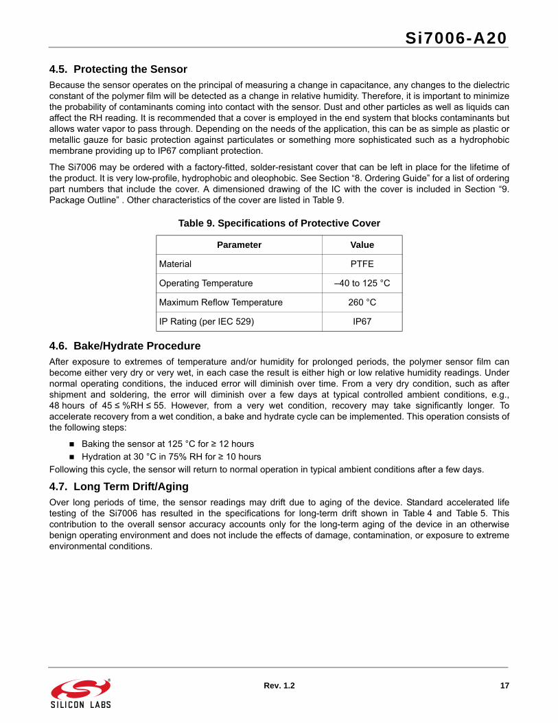
Table 9. Specifications of Protective Cover
Parameter Value
Material PTFE
Operating Temperature –40 to 125 °C
Maximum Reflow Temperature 260 °C
IP Rating (per IEC 529) IP67
Si7006-A20
18 Rev. 1.2
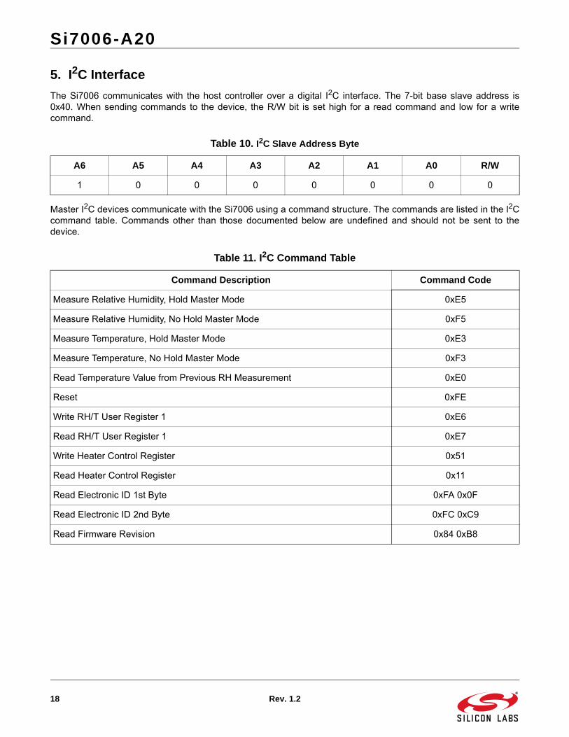
5. I2C Interface
The Si7006 communicates with the host controller over a digital I2C interface. The 7-bit base slave address is0x40. When sending commands to the device, the R/W bit is set high for a read command and low for a writecommand.
Master I2C devices communicate with the Si7006 using a command structure. The commands are listed in the I2Ccommand table. Commands other than those documented below are undefined and should not be sent to thedevice.
Table 10. I2C Slave Address Byte
A6 A5 A4 A3 A2 A1 A0 R/W
1 0 0 0 0 0 0 0
Table 11. I2C Command Table
Command Description Command Code
Measure Relative Humidity, Hold Master Mode 0xE5
Measure Relative Humidity, No Hold Master Mode 0xF5
Measure Temperature, Hold Master Mode 0xE3
Measure Temperature, No Hold Master Mode 0xF3
Read Temperature Value from Previous RH Measurement 0xE0
Reset 0xFE
Write RH/T User Register 1 0xE6
Read RH/T User Register 1 0xE7
Write Heater Control Register 0x51
Read Heater Control Register 0x11
Read Electronic ID 1st Byte 0xFA 0x0F
Read Electronic ID 2nd Byte 0xFC 0xC9
Read Firmware Revision 0x84 0xB8
Si7006-A20
Rev. 1.2 19
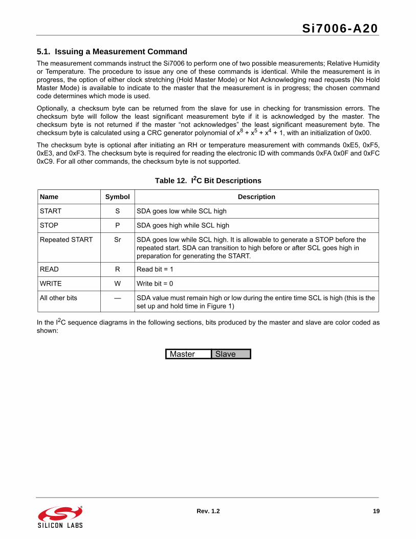
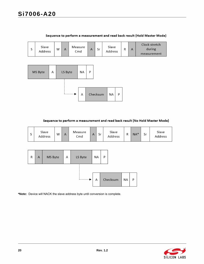
5.1. Issuing a Measurement CommandThe measurement commands instruct the Si7006 to perform one of two possible measurements; Relative Humidityor Temperature. The procedure to issue any one of these commands is identical. While the measurement is inprogress, the option of either clock stretching (Hold Master Mode) or Not Acknowledging read requests (No HoldMaster Mode) is available to indicate to the master that the measurement is in progress; the chosen commandcode determines which mode is used.
Optionally, a checksum byte can be returned from the slave for use in checking for transmission errors. Thechecksum byte will follow the least significant measurement byte if it is acknowledged by the master. Thechecksum byte is not returned if the master “not acknowledges” the least significant measurement byte. Thechecksum byte is calculated using a CRC generator polynomial of x8 + x5 + x4 + 1, with an initialization of 0x00.
The checksum byte is optional after initiating an RH or temperature measurement with commands 0xE5, 0xF5,0xE3, and 0xF3. The checksum byte is required for reading the electronic ID with commands 0xFA 0x0F and 0xFC0xC9. For all other commands, the checksum byte is not supported.
In the I2C sequence diagrams in the following sections, bits produced by the master and slave are color coded asshown:
Table 12. I2C Bit Descriptions
Name Symbol Description
START S SDA goes low while SCL high
STOP P SDA goes high while SCL high
Repeated START Sr SDA goes low while SCL high. It is allowable to generate a STOP before the repeated start. SDA can transition to high before or after SCL goes high in preparation for generating the START.
READ R Read bit = 1
WRITE W Write bit = 0
All other bits — SDA value must remain high or low during the entire time SCL is high (this is the set up and hold time in Figure 1)
Master Slave
Si7006-A20
20 Rev. 1.2
*Note: Device will NACK the slave address byte until conversion is complete.
Si7006-A20
Rev. 1.2 21
5.1.1. Measuring Relative Humidity
Once a relative humidity measurement has been made, the results of the measurement may be converted topercent relative humidity by using the following expression:
Where:
%RH is the measured relative humidity value in %RH
RH_Code is the 16-bit word returned by the Si7006
A humidity measurement will always return XXXXXX10 in the LSB field.
Due to normal variations in RH accuracy of the device as described in Table 4, it is possible for the measured valueof %RH to be slightly less than 0 when the actual RH level is close to or equal to 0. Similarly, the measured valueof %RH may be slightly greater than 100 when the actual RH level is close to or equal to 100. This is expectedbehavior, and it is acceptable to limit the range of RH results to 0 to 100%RH in the host software by truncatingvalues that are slightly outside of this range.
5.1.2. Measuring Temperature
Each time a relative humidity measurement is made a temperature measurement is also made for the purposes oftemperature compensation of the relative humidity measurement. If the temperature value is required, it can beread using command 0xE0; this avoids having to perform a second temperature measurement. The measuretemperature commands 0xE3 and 0xF3 will perform a temperature measurement and return the measurementvalue, command 0xE0 does not perform a measurement but returns the temperature value measured during therelative humidity measurement.
The checksum output is not available with the 0xE0 command.
%RH 125RH_Code65536
--------------------------------------- 6–=
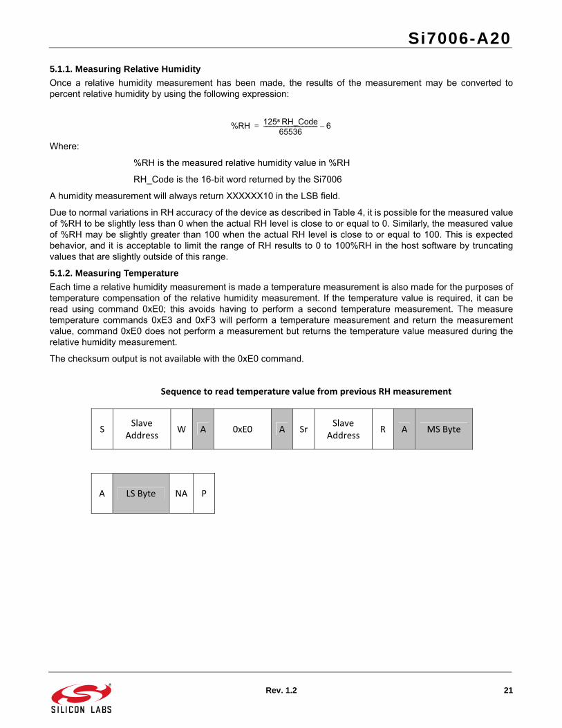
Sequence to read temperature value from previous RH measurement
S SlaveAddress W A 0xE0 A Sr Slave
Address R A MS Byte
A LS Byte NA P
Si7006-A20
22 Rev. 1.2
The results of the temperature measurement may be converted to temperature in degrees Celsius (°C) using thefollowing expression:
Where:
Temperature (°C) is the measured temperature value in °C
Temp_Code is the 16-bit word returned by the Si7006
A temperature measurement will always return XXXXXX00 in the LSB field.
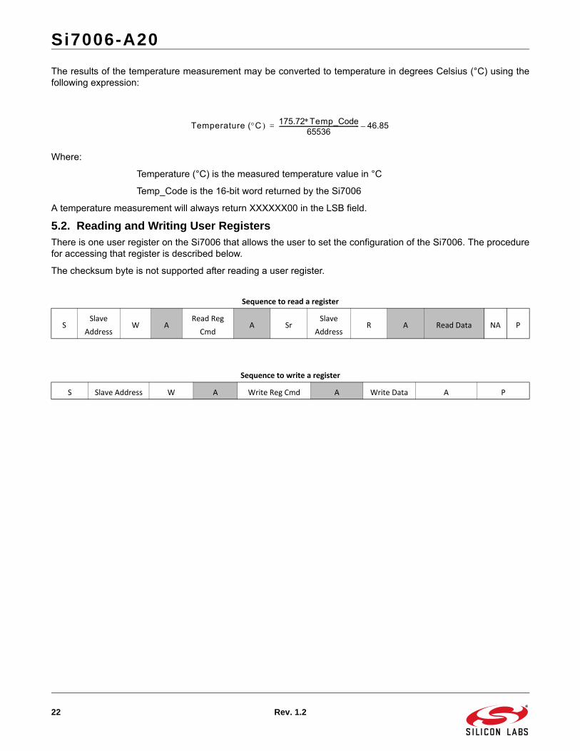
5.2. Reading and Writing User RegistersThere is one user register on the Si7006 that allows the user to set the configuration of the Si7006. The procedurefor accessing that register is described below.
The checksum byte is not supported after reading a user register.
Sequence to read a register
SSlave
AddressW A
Read Reg
CmdA Sr
Slave
AddressR A Read Data NA P
Sequence to write a register
S Slave Address W A Write Reg Cmd A Write Data A P
Temperature (C 175.72Temp_Code65536
-------------------------------------------------------- 46.85–=
Si7006-A20
Rev. 1.2 23
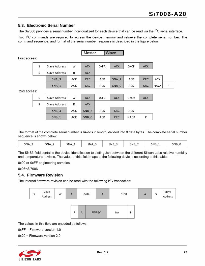
5.3. Electronic Serial NumberThe Si7006 provides a serial number individualized for each device that can be read via the I2C serial interface.
Two I2C commands are required to access the device memory and retrieve the complete serial number. Thecommand sequence, and format of the serial number response is described in the figure below:
First access:
The format of the complete serial number is 64-bits in length, divided into 8 data bytes. The complete serial numbersequence is shown below:
The SNB3 field contains the device identification to distinguish between the different Silicon Labs relative humidityand temperature devices. The value of this field maps to the following devices according to this table:
0x00 or 0xFF engineering samples
0x06=Si7006
5.4. Firmware RevisionThe internal firmware revision can be read with the following I2C transaction:
The values in this field are encoded as follows:
0xFF = Firmware version 1.0
0x20 = Firmware version 2.0
Master Slave
S Slave Address W ACK 0xFA ACK 0X0F ACK
S Slave Address R ACK
SNA_3 ACK CRC ACK SNA_2 ACK CRC ACK
SNA_1 ACK CRC ACK SNA_0 ACK CRC NACK P
2nd access:
S Slave Address W ACK 0xFC ACK 0XC9 ACK
S Slave Address R ACK
SNB_3 ACK SNB_2 ACK CRC ACK
SNB_1 ACK SNB_0 ACK CRC NACK P
SNA_3 SNA_2 SNA_1 SNA_0 SNB_3 SNB_2 SNB_1 SNB_0
SSlave
AddressW A 0x84 A 0xB8 A S
Slave
Address
R A FWREV NA P
Si7006-A20
24 Rev. 1.2
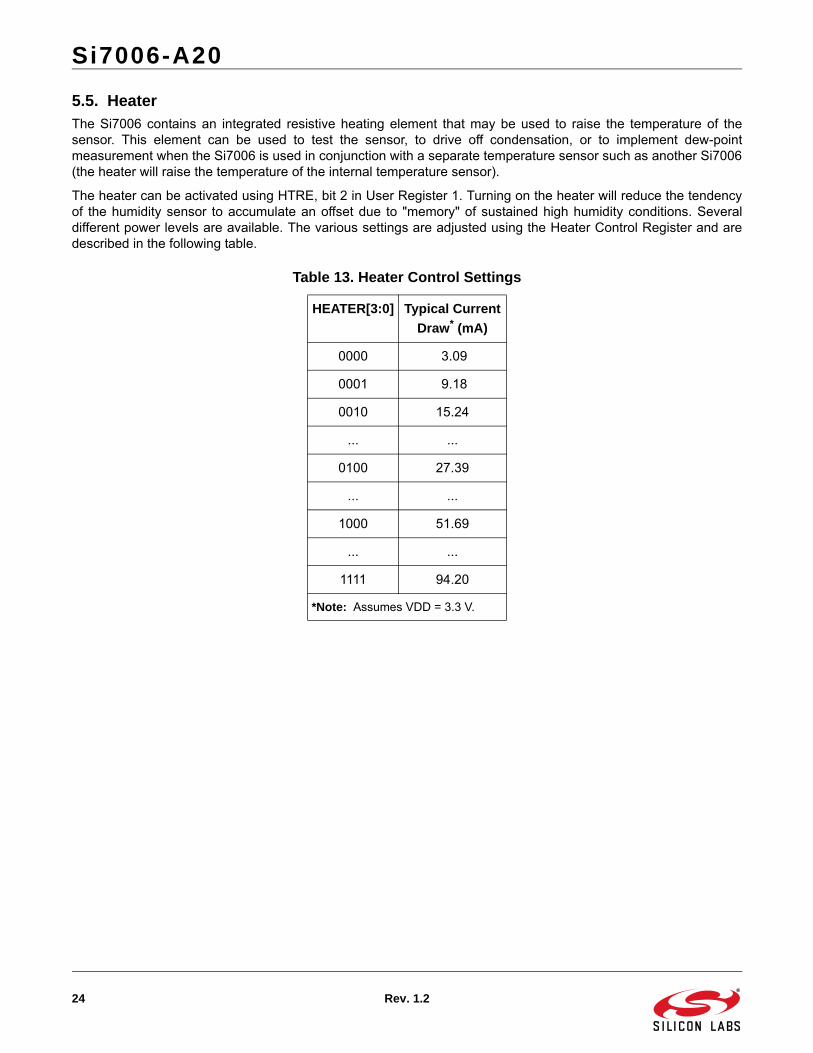
5.5. HeaterThe Si7006 contains an integrated resistive heating element that may be used to raise the temperature of thesensor. This element can be used to test the sensor, to drive off condensation, or to implement dew-pointmeasurement when the Si7006 is used in conjunction with a separate temperature sensor such as another Si7006(the heater will raise the temperature of the internal temperature sensor).
The heater can be activated using HTRE, bit 2 in User Register 1. Turning on the heater will reduce the tendencyof the humidity sensor to accumulate an offset due to "memory" of sustained high humidity conditions. Severaldifferent power levels are available. The various settings are adjusted using the Heater Control Register and aredescribed in the following table.
Table 13. Heater Control Settings
HEATER[3:0] Typical Current
Draw* (mA)
0000 3.09
0001 9.18
0010 15.24
... ...
0100 27.39
... ...
1000 51.69
... ...
1111 94.20
*Note: Assumes VDD = 3.3 V.
Si7006-A20
Rev. 1.2 25
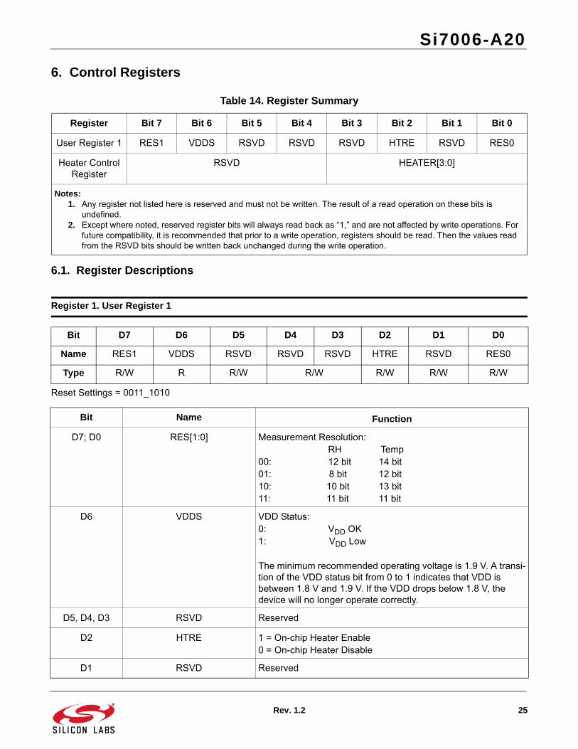
6. Control Registers
6.1. Register Descriptions
Reset Settings = 0011_1010
Table 14. Register Summary
Register Bit 7 Bit 6 Bit 5 Bit 4 Bit 3 Bit 2 Bit 1 Bit 0
User Register 1 RES1 VDDS RSVD RSVD RSVD HTRE RSVD RES0
Heater Control Register
RSVD HEATER[3:0]
Notes:1. Any register not listed here is reserved and must not be written. The result of a read operation on these bits is
undefined.2. Except where noted, reserved register bits will always read back as “1,” and are not affected by write operations. For
future compatibility, it is recommended that prior to a write operation, registers should be read. Then the values read from the RSVD bits should be written back unchanged during the write operation.
Register 1. User Register 1
Bit D7 D6 D5 D4 D3 D2 D1 D0
Name RES1 VDDS RSVD RSVD RSVD HTRE RSVD RES0
Type R/W R R/W R/W R/W R/W R/W
Bit Name Function
D7; D0 RES[1:0] Measurement Resolution:RH Temp
00: 12 bit 14 bit01: 8 bit 12 bit10: 10 bit 13 bit11: 11 bit 11 bit
D6 VDDS VDD Status: 0: VDD OK1: VDD Low
The minimum recommended operating voltage is 1.9 V. A transi-tion of the VDD status bit from 0 to 1 indicates that VDD is between 1.8 V and 1.9 V. If the VDD drops below 1.8 V, the device will no longer operate correctly.
D5, D4, D3 RSVD Reserved
D2 HTRE 1 = On-chip Heater Enable0 = On-chip Heater Disable
D1 RSVD Reserved
Si7006-A20
26 Rev. 1.2
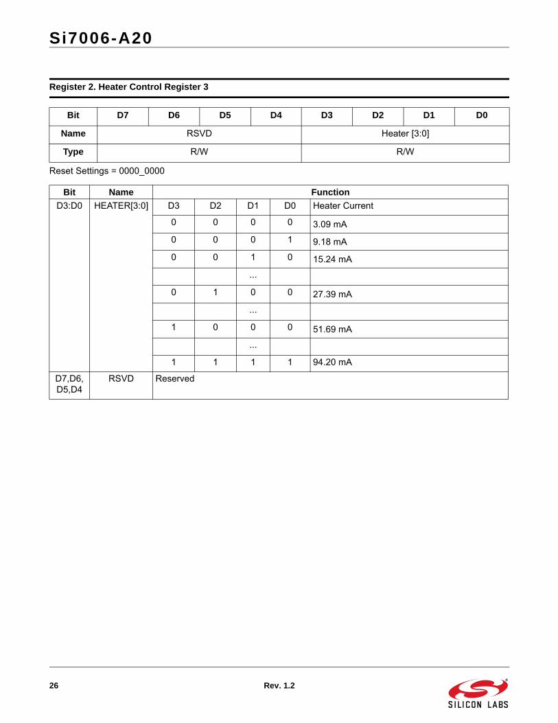
Reset Settings = 0000_0000
Register 2. Heater Control Register 3
Bit D7 D6 D5 D4 D3 D2 D1 D0
Name RSVD Heater [3:0]
Type R/W R/W
Bit Name Function
D3:D0 HEATER[3:0] D3 D2 D1 D0 Heater Current
0 0 0 0 3.09 mA
0 0 0 1 9.18 mA
0 0 1 0 15.24 mA
...
0 1 0 0 27.39 mA
...
1 0 0 0 51.69 mA
...
1 1 1 1 94.20 mA
D7,D6,D5,D4
RSVD Reserved
Si7006-A20
Rev. 1.2 27
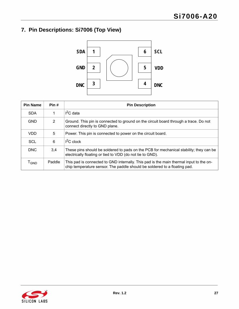
7. Pin Descriptions: Si7006 (Top View)
Pin Name Pin # Pin Description
SDA 1 I2C data
GND 2 Ground. This pin is connected to ground on the circuit board through a trace. Do not connect directly to GND plane.
VDD 5 Power. This pin is connected to power on the circuit board.
SCL 6 I2C clock
DNC 3,4 These pins should be soldered to pads on the PCB for mechanical stability; they can be electrically floating or tied to VDD (do not tie to GND).
TGND Paddle This pad is connected to GND internally. This pad is the main thermal input to the on-chip temperature sensor. The paddle should be soldered to a floating pad.
DNC
SCL
VDD
1
2
6
5GND
SDA
3 4DNC
Si7006-A20
28 Rev. 1.2
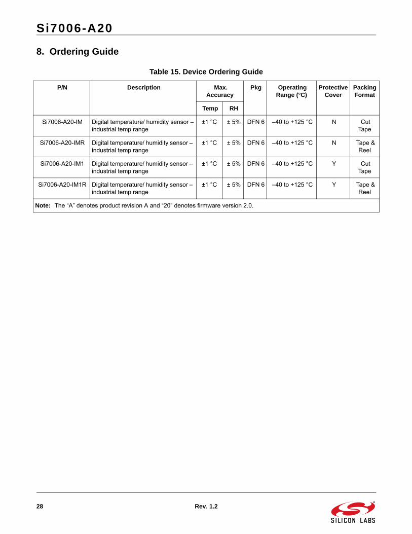
8. Ordering Guide
Table 15. Device Ordering Guide
P/N Description Max. Accuracy
Pkg Operating Range (°C)
Protective Cover
Packing Format
Temp RH
Si7006-A20-IM Digital temperature/ humidity sensor –industrial temp range
±1 °C ± 5% DFN 6 –40 to +125 °C N Cut Tape
Si7006-A20-IMR Digital temperature/ humidity sensor – industrial temp range
±1 °C ± 5% DFN 6 –40 to +125 °C N Tape & Reel
Si7006-A20-IM1 Digital temperature/ humidity sensor – industrial temp range
±1 °C ± 5% DFN 6 –40 to +125 °C Y Cut Tape
Si7006-A20-IM1R Digital temperature/ humidity sensor – industrial temp range
±1 °C ± 5% DFN 6 –40 to +125 °C Y Tape & Reel
Note: The “A” denotes product revision A and “20” denotes firmware version 2.0.
Si7006-A20
Rev. 1.2 29
9. Package Outline
9.1. Package Outline: 3x3 6-pin DFN
Figure 10. 3x3 6-pin DFN
Table 16. 3x3 6-pin DFN Package Diagram Dimensions
Dimension Min Nom Max
A 0.70 0.75 0.80A1 0.00 0.02 0.05
b 0.35 0.40 0.45
D 3.00 BSC.
D2 1.40 1.50 1.60
e 1.00 BSC.
E 3.00 BSC.
E2 2.30 2.40 2.50
H1 0.85 0.90 0.95
H2 1.39 1.44 1.49
L 0.35 0.40 0.45
aaa 0.10
bbb 0.10
ccc 0.05
ddd 0.10
eee 0.05
fff 0.05
Notes:1. All dimensions shown are in millimeters (mm).2. Dimensioning and Tolerancing per ANSI Y14.5M-1994.
Si7006-A20
30 Rev. 1.2
9.2. Package Outline: 3x3 6-pin DFN with Protective CoverFigure 8 illustrates the package details for the Si7006 with the optional protective cover. The table below lists thevalues for the dimensions shown in the illustration.
Figure 8. 3x3 6-pin DFN with Protective Cover
Table 17. 3x3 6-pin DFN with Protective Cover Package Diagram Dimensions
Dimension Min Nom Max
A — — 1.21
A1 0.00 0.02 0.05
A2 0.70 0.75 0.80
b 0.35 0.40 0.45
D 3.00 BSC.
D2 1.40 1.50 1.60
e 1.00 BSC.
E 3.00 BSC.
E2 2.30 2.40 2.50
F1 2.70 2.80 2.90
F2 2.70 2.80 2.90
h 0.76 0.83 0.90
L 0.35 0.40 0.45
R1 0.45 0.50 0.55
aaa 0.10
bbb 0.10
ccc 0.05
ddd 0.10
eee 0.05Notes:
1. All dimensions are shown in millimeters (mm).2. Dimensioning and Tolerancing per ANSI Y14.5M-1994.
Si7006-A20
Rev. 1.2 31
10. PCB Land Pattern and Solder Mask Design
Figure 9. Si7006 PCB Land Pattern
Table 18. PCB Land Pattern Dimensions
Symbol mm
C1 2.90
E 1.00
P1 1.60
P2 2.50
X1 0.45
Y1 0.85
Notes:General
1. All dimensions shown are at Maximum Material Condition (MMC). Least Material Condition (LMC) is calculated based on a Fabrication Allowance of 0.05 mm.
2. This Land Pattern Design is based on the IPC-7351 guidelines.Solder Mask Design
3. All metal pads are to be non-solder mask defined (NSMD). Clearance between the solder mask and the metal pad is to be 60 µm minimum, all the way around the pad.
Stencil Design
4. A stainless steel, laser-cut and electro-polished stencil with trapezoidal walls should be used to assure good solder paste release.
5. The stencil thickness should be 0.125 mm (5 mils).6. The ratio of stencil aperture to land pad size should be 1:1 for all perimeter pins.7. A 2x1 array of 1.00 mm square openings on 1.30 mm pitch should be used for the
center ground pad to achieve a target solder coverage of 50%.Card Assembly
8. The recommended card reflow profile is per the JEDEC/IPC J-STD-020 specification for Small Body Components.
Si7006-A20
32 Rev. 1.2
11. Top Marking
11.1. Si7006 Top Marking
11.2. Top Marking Explanation
Mark Method: Laser
Font Size 0.30 mm
Pin 1 Indicator: Circle = 0.30 mm DiameterUpper-Left Corner
Line 1 Marking: TTTT = Mfg Code
Si7006-A20
Rev. 1.2 33
12. Additional Reference Resources
AN607: Si70xx Humidity Sensor Designer’s Guide
Si7006-A20
34 Rev. 1.2
DOCUMENT CHANGE LIST
Revision 0.9 to Revision 0.91 Updated Table 2 on page 4.
Revision 0.91 to Revision 1.0 Rolled revision number to 1.0.
Revision 1.0 to Revision 1.1 Updated Footnote 2 in Table 3 on page 5.
Updated Section “4.5. Protecting the Sensor”
Updated Table 9 on page 17.
Corrected a typo in the I2C sequence for no-hold mode in Section “5.1. Issuing a Measurement Command” .
Corrected a typo in Table 12 on page 19.
Updated Table 17 on page 30 dimensions F1 and F2.
Revision 1.1 to Revision 1.2 Updated diagram in "5.4. Firmware Revision" on page 23.
Updated notes in Table 18, “PCB Land Pattern Dimensions,” on page 31.
Changed packing format from tube to cut tape for all non-tape & reel part numbers without protective filter covers.

DisclaimerSilicon Laboratories intends to provide customers with the latest, accurate, and in-depth documentation of all peripherals and modules available for system and software implementers using or intending to use the Silicon Laboratories products. Characterization data, available modules and peripherals, memory sizes and memory addresses refer to each specific device, and "Typical" parameters provided can and do vary in different applications. Application examples described herein are for illustrative purposes only. Silicon Laboratories reserves the right to make changes without further notice and limitation to product information, specifications, and descriptions herein, and does not give warranties as to the accuracy or completeness of the included information. Silicon Laboratories shall have no liability for the consequences of use of the information supplied herein. This document does not imply or express copyright licenses granted hereunder to design or fabricate any integrated circuits. The products must not be used within any Life Support System without the specific written consent of Silicon Laboratories. A "Life Support System" is any product or system intended to support or sustain life and/or health, which, if it fails, can be reasonably expected to result in significant personal injury or death. Silicon Laboratories products are generally not intended for military applications. Silicon Laboratories products shall under no circumstances be used in weapons of mass destruction including (but not limited to) nuclear, biological or chemical weapons, or missiles capable of delivering such weapons.
Trademark InformationSilicon Laboratories Inc., Silicon Laboratories, Silicon Labs, SiLabs and the Silicon Labs logo, CMEMS®, EFM, EFM32, EFR, Energy Micro, Energy Micro logo and combinations thereof, "the world’s most energy friendly microcontrollers", Ember®, EZLink®, EZMac®, EZRadio®, EZRadioPRO®, DSPLL®, ISOmodem ®, Precision32®, ProSLIC®, SiPHY®, USBXpress® and others are trademarks or registered trademarks of Silicon Laboratories Inc. ARM, CORTEX, Cortex-M3 and THUMB are trademarks or registered trademarks of ARM Holdings. Keil is a registered trademark of ARM Limited. All other products or brand names mentioned herein are trademarks of their respective holders.
http://www.silabs.com
Silicon Laboratories Inc.400 West Cesar ChavezAustin, TX 78701USA
Smart.Connected.Energy-Friendly
Productswww.silabs.com/products
Qualitywww.silabs.com/quality
Support and Communitycommunity.silabs.com