semiconductor tcad fabrication development for bcd technology
TRANSCRIPT
i
Semiconductor TCAD Fabrication Development for BCD Technology
A Major Qualifying Project Report:
submitted to the Faculty
of the
WORCESTER POLYTECHNIC INSTITUTE
in partial fulfillment of the requirements for the
Degree of Bachelor of Science
by
____________________________
Matthew Hazel
_____________________________
Marc Cyr
Date: March 13, 2006
Submitted to:
_____________________________
Professor John McNeill, Co-Advisor
ii
Abstract
As semiconductor devices evolve, it is important to understand the fabrication
processes and issues that arise with each new generation of transistor technology.
Through research, and the use of the SILVACO simulation tools, we successfully
simulated and tested a series of Bipolar, CMOS, and DMOS devices, and optimized them
in order to minimize issues such as leakage current and punch through. Additionally,
comparisons between actual, and theoretical device characteristics were made.
iii
Acknowledgements We take this opportunity to thank the people that have supported us over the
course of our project. Without their help and guidance, we would not have been able to
complete this effort in a timely manner.
Professor Shela Aboud (Project Advisor): Whose knowledge of BCD
technologies as well as the Silvaco simulation tools was a significant help
during the completion of our project.
Professor John McNeill (Project Advisor): For graciously taking on the role of
our project advisor for the third term, and completion of our MQP.
Jim McClay: Whose research paper on device fabrication proved to be the
foundation of this project.
iv
Table of Contents Abstract...........................................................................................................................ii
Acknowledgements ........................................................................................................iii
Table of Contents ........................................................................................................... iv
List of Figures..............................................................................................................viii
List of Tables ..................................................................................................................x
Executive Summary .......................................................................................................xi
1. Introduction..............................................................................................................1
2. Background ..............................................................................................................3
2.1. Evolution of the Transistor in BCD Technology ................................................3
2.2. The Fabrication Process.....................................................................................4
2.2.1. Lithography ................................................................................................5
2.2.2. Oxidation of Silicon....................................................................................5
2.2.3. Diffusion and Ion Implantation ...................................................................6
2.2.4. Ion Implantation..........................................................................................6
2.2.5. Film Deposition ..........................................................................................7
2.3. BCD Masking Process .......................................................................................7
2.3.1. Locos Isolation ...........................................................................................8
3. Silvaco Software Suite............................................................................................ 10
3.1. How to Code with Athena................................................................................ 10
3.1.1. Overview .................................................................................................. 10
3.1.2. Research ................................................................................................... 12
3.1.3. Line-By-Line Analysis.............................................................................. 13
3.2 How to Code with Atlas.................................................................................... 13
3.2.1. Overview .................................................................................................. 13
3.2.2. Research ................................................................................................... 15
3.3. Deviance from Ideal Simulation Examples....................................................... 16
3.3.1. Mesh Lines ............................................................................................... 16
3.3.2. Oxidation.................................................................................................. 16
3.3.3. Masking.................................................................................................... 18
v
3.3.4. LOCOS Isolation process.......................................................................... 20
3.3.5. Contacts.................................................................................................... 27
3.4. Conclusion....................................................................................................... 29
4. CMOS Transistor ................................................................................................... 30
4.1. Problem Statement........................................................................................... 30
4.2. Theoretical Device Characteristics................................................................... 31
4.2.1. Oxide Thickness ....................................................................................... 31
4.2.2. Threshold Voltage..................................................................................... 32
4.2.3. I-V Characteristics .................................................................................... 33
4.3. Walkthrough of CMOS Fabrication ................................................................. 34
4.3.1. PMOS Fabrication Summary .................................................................... 36
4.3.2. NMOS Device Process.............................................................................. 37
4.4. Final Device Characteristics and Comparison .................................................. 43
4.4.1. Gate Oxide................................................................................................ 43
4.4.2. Threshold Voltage..................................................................................... 44
4.4.3. I-V Relationship........................................................................................ 45
4.5. Conclusion....................................................................................................... 46
5. Bipolar Junction Transistor..................................................................................... 48
5.1. Problem Statement........................................................................................... 48
5.2. Theoretical Device Characteristics................................................................... 49
5.2.1. Gummel Plot............................................................................................. 49
5.2.2. I-V Characteristics .................................................................................... 50
5.3. Walkthrough of BJT Fabrication...................................................................... 51
5.3.1. BJT Device Process .................................................................................. 53
5.4. Final Device Characteristics and Comparison .................................................. 58
5.4.1. Gummel Plot............................................................................................. 59
5.4.2. I-V Characteristics .................................................................................... 61
5.5. Conclusion....................................................................................................... 62
6. LDMOS Transistor................................................................................................. 62
6.1. Problem Statement........................................................................................... 62
6.2. Theoretical Device Characteristics................................................................... 63
vi
6.2.1. Threshold Voltage..................................................................................... 64
6.2.2. Leakage Current........................................................................................ 64
6.2.3. Off-State Leakage Current ........................................................................ 65
6.2.4. Breakdown Voltage .................................................................................. 66
6.2.5. On-Resistance........................................................................................... 67
6.2.6. On-State Drain Current ............................................................................. 68
6.2.7. Capacitance............................................................................................... 68
6.3. Walkthrough of LDMOS Fabrication............................................................... 69
6.4. Final Device Characteristics and Comparisons................................................. 78
6.4.1.Id =(Vd, Vg) Characteristic............................................................................. 79
6.4.2.Transistion Potential vs Vg, Vd...................................................................... 80
6.4.3.Cdd vs Vd, Vg................................................................................................. 80
6.5 Conclusion ........................................................................................................... 81
7. BCD Fabrication Wafer.......................................................................................... 83
7.1. Problem Statement........................................................................................... 83
7.2. Process Recipe................................................................................................. 83
7.3. Strategies for maximizing Performance Parameters ......................................... 85
7.3.3. Process Problems ...................................................................................... 86
7.4. Strategies For Improving Shrinking Device Geometry ..................................... 86
7.4.1 VLSI technology shrinking Poly-Silicon Window...................................... 86
7.4.2. Trench gate structure................................................................................. 86
7.4.3. Materials................................................................................................... 87
7.4.4. Tapered Oxide (TEOS) ............................................................................. 87
7.5. Conclusion....................................................................................................... 87
8. Project Summary and Future Work......................................................................... 88
Appendix A – References.............................................................................................. 90
Appendix C – PMOS Athena and Atlas Code................................................................ 98
Appendix D – BJT Athena and Atlas Code.................................................................. 104
Appendix E – LDMOS Athena and Atlas Code ........................................................... 110

vii
viii
List of Figures Figure 2-2 Atlas Coding Process ................................................................................... 14
Figure 3-3 Rounded Oxide ............................................................................................ 17
Figure 3-4 Bird Beak Effect .......................................................................................... 18
Figure 3-5 Nitride Mask Layer ...................................................................................... 19
Figure 3-6 After Nitride Mask Layer ............................................................................. 19
Figure 3-7 Implantation During Mask Step.................................................................... 20
Figure 3-11 Before Diffusion ........................................................................................ 25
Figure 3-12 After Diffusion........................................................................................... 26
Figure 3-13 Juntion Lines.............................................................................................. 27
Figure 3-14Plated Aluminum Contacts.......................................................................... 28
Figure 3-15 Etched Aluminum Contacts........................................................................ 28
Figure 4-1: Oxidation thickness versus time for wet and dry O2..................................... 32
Figure 4-2: CMOS Design flow chart ............................................................................ 35
Figure 4-3: N-Channel MOSFET Device....................................................................... 37
Figure 4-4: P-Channel MOSFET Device ....................................................................... 37
Figure 4-5: P-Type wafer with Arsenic Epitaxial Layer................................................. 38
Figure 4-6: Boron Well Drive........................................................................................ 39
Figure 4-7: Upper surface of NMOS transistor .............................................................. 40
Figure 4-8: Implanted Arsenic and grown shielding oxide ............................................. 41
Figure 4-9: NMOS transistor after Arsenic Diffusion .................................................... 42
Figure 4-10: Completed NMOS transistor ..................................................................... 43
Figure 4-11: NMOS Conductivity versus Gate Bias....................................................... 45
Figure 4-12: I-V Curve for NMOS transistor ................................................................. 46
Figure 5-1: Ideal and Non-Ideal Gummel Plots (Pierret, p. 425) .................................... 50
Figure 5-2: Sample Ideal I-V characteristics for a PNP BJT (Pierret, p. 408) ................. 51
Figure 5-3: BJT Process Recipe..................................................................................... 52
Figure 5-4: Simplified BJT Structure............................................................................. 53
Figure 5-5: BJT after epitaxial growth........................................................................... 54
Figure 5-6: BJT post Boron Diffusion ........................................................................... 55
ix
Figure 5-7: BJT post Arsenic Implantation .................................................................... 56
Figure 5-8: BJT Post Arsenic Collector Implant ............................................................ 57
Figure 5-9: BJT Post Aluminum Deposition.................................................................. 58
Figure 5-10: Completed BJT Structure .......................................................................... 58
Figure 5-11: Non-Ideal Gummel plot............................................................................. 59
Figure 5-12: Gummel Plot without SRH Model............................................................ 60
Figure 5-13: BJT I-V Characteristics............................................................................. 61
Figure 6-7 LDMOS 2nd Oxide Layer ............................................................................ 76
Figure 6-8 LDMOS P-Well Drive ................................................................................. 77
Figure 6-9 Final LDMOS Device .................................................................................. 78
Figure 6-11 Vdi vs Vd, Vg .............................................................................................. 80
Figure 6-12 Cgg vs Vd .................................................................................................... 81
x
List of Tables Table 2-1: device characteristics of BCD-I though BCD-V .............................................4
Table 3-1: Threshold Voltage Symbol Explanation ....................................................... 33
Table 3-2: Saturation Current Symbol Explanation........................................................ 34
Table 3-3: CMOS Masking Steps .................................................................................. 36
xi
Executive Summary As the semiconductor industry continues to mature, technological advancements
have allowed for the scaling down of BCD devices to submicron dimensions. As these
devices decrease in size, their complexity increases and device issues such as leakage
current, latch-up, isolation, and 2nd order transients all become more prevalent. In order
to isolate these issues, and develop a fabrication process which minimizes their effect,
software packages have been developed in order to simulate both the creation process and
BCD device behavior.
Silvaco is one such software package that has been developed in order to provide
a complete simulation tool for both the fabrication process as well as modeling completed
device behavior. This project focused on the use of Athena and Atlas, which are part of
the Silvaco suite of modeling applications, in order to create a 10 mask fabrication
process encompassing all of the BCD devices. Additionally, research was conducted into
the evolution of BCD technology, as well as many aspects of the fabrication process.
We researched the lithography process. A strong grasp of the fabrication process
was necessary to perform the analysis that would occur later in the project. In addition,
we researched the evolution of the transistor, past and future. We did so, in hopes that we
could learn the direction of technology, so that we may more accurately apply it to our
simulations.
The initial device which was modeled was an NMOS transistor. Research
conducted on the theoretical behavior of an NMOS transistor would be the basis for
which we measured our success in developing this device. As this was our first
experience with using Athena to generate a device of any sort we began by modifying an
existing example. Incremental changes were made between simulations, and by viewing
their effects on the device’s behavior and characteristics we were able to understand the
coding language used by Athena and Atlas.
Athena is used to generate results for device behavior, and it was these results
which were compared against the theoretical behaviors. In most cases, our NMOS
transistor demonstrated acceptable behavior. An acceptable turn-on voltage, I-V
characteristic, and oxide thickness were all obtained with the NMOS device.
xii
The second of three devices which we were to simulate was a bipolar junction
transistor (BJT). Rather than modify an existing example, this device was to be designed
from scratch. Physical parameters were chosen so that the BJT would roughly
correspond in size to the NMOS transistor, and the process flow was created so that it
could be implemented alongside the process flow of the NMOS transistor. As BCD
technology requires the simultaneous development of several different types of devices
on the same wafer, it was necessary to make these size and process considerations.
During the process of modeling the BJT, we both refined and expanded our
knowledge of Atlas and Athena, allowing for a much more rapid development process.
Again, research into the theoretical behavior of a BJT would prove to be the basis for
which we determined the success of our device. Careful consideration of the doping
characteristics for the base, emitter and collector, as well as knowledge of the constraints
placed on the geometry of the BJT allowed us to create a device that again demonstrated
acceptable operating characteristics.
The final device we modeled was the LDMOS. We further learned how to
simulate a device we had never even seen prior to this project. We used our step-by-step
process to fabricate the LDMOS on the wafer. We learned of the double diffused
transistor and the drift length.
The final step of the project involved placing all the devices on a single wafer.
We thought of the strategies of changing p and n type dopants at the cost of BJT
amplification or LDMOS on-resistance. We learned about the tradeoffs of high
switching speeds for the CMOS and how that put the LDMOS at risk of punch through.
We designed a single process recipe that accounted for accommodating all the needs of
each individual device, only on a single wafer.
Through the research conducted into both the fabrication process as well as the
evolution of BCD technology and its components, we were able to generate three devices
which demonstrated acceptable operating characteristics. Our knowledge of
semiconductor development, and the tradeoffs which must be considered when
developing separate technologies on an individual silicon wafer has greatly increased.
We achieved our goal of creating a ten-mask process for BCD technology, and in the

xiii
process learned how to program using one of the industry’s most widely accepted
software packages for semiconductor device modeling.
1
1. Introduction As the semiconductor industry continues to mature, technological advancements
have allowed for the scaling down of BCD devices to submicron dimensions. BCD is the
name given to an integrated circuit (IC) composed of Bipolar Junction Transistors
(Bipolar), Complimentary Metal-Oxide-Semiconductor Field-Effect Transistors (CMOS),
and Lateral Double Diffused Metal Oxide Semiconductor Field-Effect Transistor
(LDMOS). As these devices decrease in size, their complexity increases and device
issues such as leakage current, punch-through, isolation, and 2nd order transients all
become more prevalent.
In order to isolate these issues, and develop a fabrication process, which
minimizes their effect, software packages have been developed in order to simulate both
the creation process and BCD device behavior. The Silvaco suite of applications,
including TonyPlot, Athena, and Atlas, is just one such software package that is
commonly used in industry in order to simulate the BCD fabrication process. Silvaco has
gained broad acceptance in the semiconductor industry as being a reliable and accurate
simulation tool for the development of BCD devices.
Within Silvaco there are complex non-ideality models which account for such
device behaviors as average minority carrier lifetime (Shockley-Read-Hall), or doping
impurities arising during the annealing process. Silvaco allows designers to efficiently
test a masking process, and then analyze the resulting device without having to physically
create the device on a silicon wafer. This saves designers both time and money, and
software packages like Silvaco have become an invaluable tool in the semiconductor
industry.
The goal of this project is to use Silvaco to successfully simulate a 10 mask
process corresponding to BCD III technology parameters, and then analyze the issues that
would arise were we to attempt a BCD V device. We intend to simulate a CMOS
transistor, BJT transistor, and LDMOS device, and although each of the devices is
simulated independently to reduce the computational burden of the software package,
each device will be treated as if it were fully integrated on the same silicon wafer. The
processing steps must then be optimized to create the “best” devices while still adhering
2
to BCD III standards. There are numerous parameter tradeoffs between devices, such as
diffusion depth, sheet resistance vs. turn on voltage, complexity vs. cost, breakdown
voltages, and other device parameters that are dependent upon the doping profile.
In addition to the fabrication process, we will explore the expected, theoretical
behavior of these BCD devices, and then use Silvaco to extract performance parameters,
such as the sheet resistance, turn-on voltage, I-V curves, reverse breakdown voltage, and
more. Comparisons can then be made between the expected behavior and the simulated
behavior of the devices. Then, time can be spent to fine tune the doping profiles and
physical geometry of the device in order to achieve optimal results.
This report is organized so that the reader will first acquire an understanding of
the evolution of the BCD components. Then, an overview of the BCD fabrication
process is presented, including the most common methodologies used. Once the
background information has been concluded, a more in depth analysis of three separate
BCD technologies is presented. Each analysis will begin with a description of the
theoretical performance characteristics, followed by a description of the fabrication
process, and then completed with a comparison between the generated results and the
theoretical expectations.
3
2. Background The need for higher power switching applications is increasing as technology
advances. Power supplies, current sources, battery chargers, boost/buck converters,
computer processors etc. are requiring more power switching and less silicon. The
transistor has come along way since its creation. This chapter will discuss the evolution
of the transistor and the means to fabricate it.
2.1. Evolution of the Transistor in BCD Technology
Until the eighties, BJT’s were the main technology used for Power IC’s. The BJT
was the best transistor for his application because of its “amplification and matching
properties”. BJT I2L was used to implement the gate logic at that time. Soon, the high
demand for gate logic led to the need for a better switching technology. The BJT I2L
then became outdated because of its power consumption needs and complex design. At
low frequencies, CMOS was the apparent choice for gate logic design. Power IC’s
expanded to include BJT and CMOS technology. BJT’s reached a limit in delivering
power to the load. The DMOS overcame these limitations. Virtually no DC driving
current is required for the DMOS. With the addition of the DMOS to the BJT and
CMOS, a new form of technology was created, BCD technology. 1
BCD technology itself has gone through multiple stages of change and evolution.
As the demand of complex designs increased, so did cost. Eventually BCD technology
had to take up less real estate, other wise its evolution would be coming to an end.
Instead of increasing the die size, the designers came up with an alternative
solution to increase space; they would reduce the size requirement of the BCD
technology from 4µ to 2.5 µ. This allowed almost three times the density of transistors
on the same size chip. Also, lower threshold voltages were obtained. BCD-I had a
threshold of 1.3V while the new device, which had a smaller width, (named BCD II
technology) boasted a threshold voltage of 1.1V. Now signal component density and
power current density parameters were nearly doubled.2
1 Smart Power IC’s pg. 1 2 Ibid pg. 2-8
4
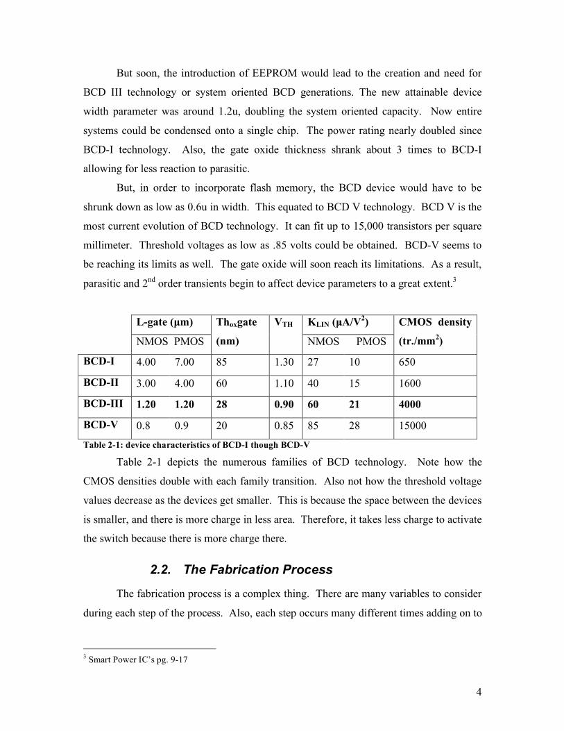
But soon, the introduction of EEPROM would lead to the creation and need for
BCD III technology or system oriented BCD generations. The new attainable device
width parameter was around 1.2u, doubling the system oriented capacity. Now entire
systems could be condensed onto a single chip. The power rating nearly doubled since
BCD-I technology. Also, the gate oxide thickness shrank about 3 times to BCD-I
allowing for less reaction to parasitic.
But, in order to incorporate flash memory, the BCD device would have to be
shrunk down as low as 0.6u in width. This equated to BCD V technology. BCD V is the
most current evolution of BCD technology. It can fit up to 15,000 transistors per square
millimeter. Threshold voltages as low as .85 volts could be obtained. BCD-V seems to
be reaching its limits as well. The gate oxide will soon reach its limitations. As a result,
parasitic and 2nd order transients begin to affect device parameters to a great extent.3
L-gate (µm) KLIN (µA/V2)
NMOS PMOS
Thoxgate
(nm)
VTH
NMOS PMOS
CMOS density
(tr./mm2)
BCD-I 4.00 7.00 85 1.30 27 10 650
BCD-II 3.00 4.00 60 1.10 40 15 1600
BCD-III 1.20 1.20 28 0.90 60 21 4000
BCD-V 0.8 0.9 20 0.85 85 28 15000
Table 2-1: device characteristics of BCD-I though BCD-V
Table 2-1 depicts the numerous families of BCD technology. Note how the
CMOS densities double with each family transition. Also not how the threshold voltage
values decrease as the devices get smaller. This is because the space between the devices
is smaller, and there is more charge in less area. Therefore, it takes less charge to activate
the switch because there is more charge there.
2.2. The Fabrication Process
The fabrication process is a complex thing. There are many variables to consider
during each step of the process. Also, each step occurs many different times adding on to
3 Smart Power IC’s pg. 9-17
5
further complexities. In this chapter each step of the fabrication process will be discussed
in great detail.
2.2.1. Lithography
The term lithography equates to a term that analog designers and manufacturers
know as a ‘mask’. The number of masking steps in a given fabrication process acts as a
rubric for determining both complexity and cost of that process.
The first step in the lithographical process is to clean the wafer. After it has been
cleaned we can then deposit some barrier layer. This layer serves to protect the silicon
from damage, when the layer is later stripped. The photo-resist is then put on top of the
barrier metal. To ensure the photo-resist, the metal, and the silicon are bonded well, the
wafer is soft-baked.
It is here that we begin our very precise masking steps. The masks are placed
over the wafer in a specific manner to either mask away the area or mask around the area
depending on the type of resist used. The resist is then exposed to high intensity ultra
violet light leaving the desired part and etching away the unwanted material.4
2.2.2. Oxidation of Silicon
Heating silicon up to high temperatures in the presence of water vapor or oxygen
results in the creation of silicon dioxide, a major component in the creation of BCD
technology. The main factors in determining the growth of silicon have to do with the
atmosphere in which the silicon is annealed, the time it is annealed, the temperature in
which it is annealed, the crystal orientation, and the doping of the impurity atoms.
There are generally two types of growth processes that silicon can be grown in, a
wet oxidation process and a dry oxidation process. The dry process involves an
atmosphere of oxygen, and the wet involves the presence of water vapors. The dry
process is usually reserved for slower growth rates, as used in MOS technology. The wet
process is a much faster growth rate and is used more for making thick masking layers.
4 Introduction to Microelectronic Fabrication pg. 13-27
6
Time and temperature are large factors for the growth of oxidation. The longer
time the silicon is heated, and the higher the temperature, the thicker the masking layer
becomes.
The type of dopant of the impurity atoms has an affect on the oxidation growth as
well. “Boron and gallium tend to be depleted from the surface, whereas phosphorus and
arsenic… pile up at the surfaces”.5 “Mobility reaches a maximum value at low impurity
concentrations; (in gallium arsenide and silicon) this corresponds to the lattice-scattering
limitation. Both electron and hole motilities decrease with increasing impurity
concentration and eventually approach a minimum value at high concentrations.”6 This
means that the acceptors diffuse more quickly than the donors. However, the diffusion
reaches its maximum more quickly.
Also, the number of times a silicon layer is heated affects the rate of growth. The
more times, the thicker the layer becomes.
Silicon nitride is an effective substance to mask silicon dioxide.7
2.2.3. Diffusion and Ion Implantation
The process of diffusion has a great impact upon the size measurements of a given
device. Diffusion controls junction distances, laterally and vertically, sheet resistance,
which directly correlates to Ron of the LDMOS.
Diffusion is controlled once again by an annealing process. Diffusion annealment
is done typically longer than oxidation growth. This is because its sole purpose to expand
the region of concentration to create the proper junctions in a device, which influence the
channel/well specifications.
The same factors exist throughout the process of diffusion as exist in growth
oxidation.8
2.2.4. Ion Implantation
Ion implantation is used as a step in the fabrication process to place some
impurity concentration projected at some range, into a layer of the device being made. 5 Introduction to Microelectronic Fabrication pg.38 6 Semi-conductor Devices Physics And Technology pg. 33 7 Intrduction to Microelectronic Fabrication pg. 29-47 8 Semi-conductor Devices Physics And Technology pg. 49-83
7
The distance that the impurity concentration is spread into the material is based on a
Gaussian distribution. The projected range that the ion implantation goes is based on the
acceleration energy. Typically it is used for shallow PN junctions because of the
Gaussian distribution. In reality, the curve is not exactly Gaussian; there are some
deviations.9
2.2.5. Film Deposition
CVD forms a thin film on the surface by thermal decomposition. The desired
material is then placed there directly from its gaseous form.
To apply the contacts to the device at hand, a step of film deposition is necessary.
Chemical Vapor Deposition (CVD) is a common way to apply the contacts. A mask
layer is applied, and then the contacts are plated onto the exposed areas of the device.
CVD is also a common way to apply the epitaxial layer, or the “seed” layer.10
2.3. BCD Masking Process
In this section of the report, the masking process of BCD fabrication will be
discussed. This section is independent of simulations or the simulation process.
Figure 2-1 BCD Wafer Cross Section
Figure 2-1 shows an example of a cross section of a BCD wafer. This example
uses junction isolation and lacks an epitaxial layer, so it is quite unlike the example in the
report which uses LOCOS isolation and has an N-type epitaxial layer on all the devices
9 Semi-conductor Devices Physics And Technology pg. 89-105 10 Semi-conductor Devices Physics And Technology pg. 107-129
8
except for the N-channel MOSFET. In this figure, additional N-well’s have been created
in the absence of the epitaxial layer.
2.3.1. Locos Isolation
Device isolation is an important part of BCD technology. The affects of one
device should not be felt by other devices on the same chip. That would result in flawed
chips, and large unwanted expenses. To avoid this scenario, techniques of device
isolation can be applied. There are three main types of device isolation. Trench isolation,
junction isolation, and locos isolation.
Trench isolation involves physically cutting a small trench between two devices
on a chip. In other words, there is actually a piece of silicon missing in-between the two
devices. This method is somewhat complicated, and does not work well with very small
devices for two reasons. First of all, the trench cutting machine can only cut so small.
Secondly, as the devices gets smaller, the trench separating the devices also gets smaller.
Thus, parasitic effects can begin to affect devices mutually.
Another type of isolation is called junction isolation. This method is preferred
most of the time. It is cheap, quick and easy. This method involves separating two
devices by creating a junction doped with the opposite impurity concentration as the
devices it surrounds. In this manner, the junction effectively acts like a diode, not letting
current pass to and from either device. The drawbacks of this method of isolation are
more noticeable in BCD-V technology. As the device gets smaller, the junctions become
closer together. Essentially, adding another junction may create an additional transistor
or NPN junction where one is not wanted. Under certain conditions, that transistor can
turn on, ruining the parameters of the original device.11
The last type of isolation is known as LOCOS isolation. This method is easy to
implement. This method of isolation involves growing an oxide layer between two
devices. This way, the oxide isolates the two devices. The problem with LOCOS
isolation is that it may require some maneuvering of masking steps, and may require an
11 Power IC’s pg.3-6

9
extra masking step in order to isolate that oxide from being improperly doped by an
impurity concentration.12
12 Characteristics of P-channel SOI
10
3. Silvaco Software Suite Athena, Atlas, Tonyplot comprise the Silvaco Suite of applications. Each of them
have their distinct uses and powerful applications. Athena is used for creating the
fabrication design process. Atlas is used for modeling fabricated designs and extracting
device parameters. Tonyplot is used for creating visual representations of the coded
simulations. Together, they accurately allow a user to simulate and test devices of a
production wafer fabrication process.
3.1. How to Code with Athena
Figure 3-1 is a representation of the coding process we learned to use out of
necessity. Initially the project seems very overwhelming. However, after we created a
goal relating to a general problem statement, an outline, and a step-by-step process, the
project was finished soon. We held the same idea to coding with Athena. At first, coding
an entire device seemed difficult. After going step-by-step, the project was fairly easy to
finish.
3.1.1. Overview
Presented is a conceptual diagram and overview of the Athena coding process.
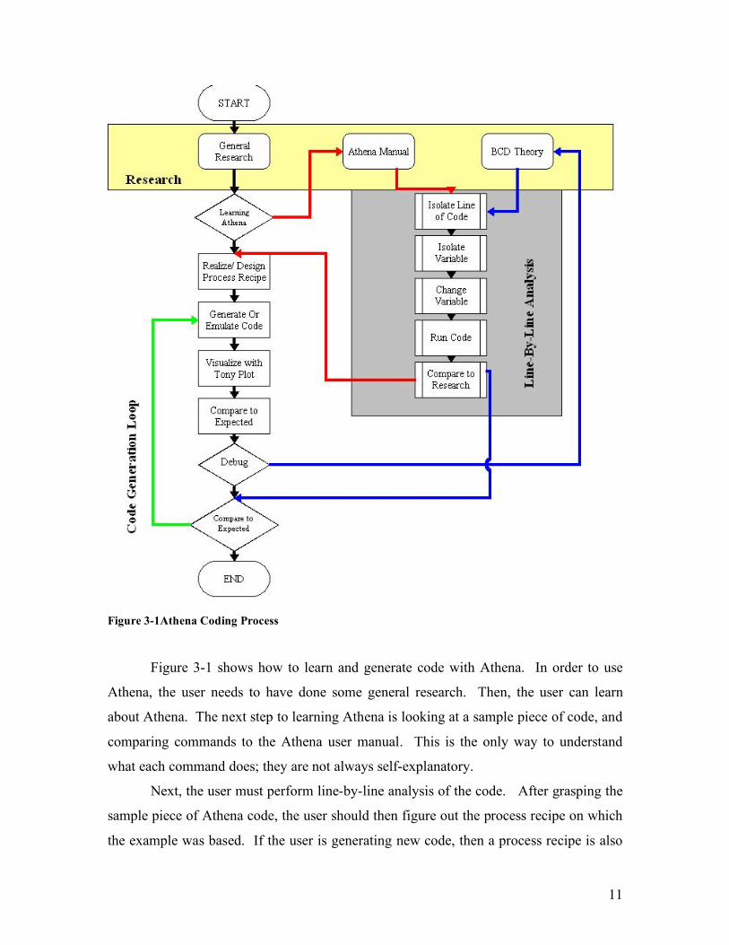
11
Figure 3-1Athena Coding Process
Figure 3-1 shows how to learn and generate code with Athena. In order to use
Athena, the user needs to have done some general research. Then, the user can learn
about Athena. The next step to learning Athena is looking at a sample piece of code, and
comparing commands to the Athena user manual. This is the only way to understand
what each command does; they are not always self-explanatory.
Next, the user must perform line-by-line analysis of the code. After grasping the
sample piece of Athena code, the user should then figure out the process recipe on which
the example was based. If the user is generating new code, then a process recipe is also
12
necessary. Once the process recipe has been created, the user can then generate (or
emulate existing code). Next, the user must visualize the code and compare it to the
expected results (from research).
At this point, the Athena code may possess errors or undesired results. If that is
the case, the user has to debug the code. Doing this involves the same line-by-line
process as learning Athena. Isolate the line of code and the variable (by commenting out
the desired piece of code) and see how it affects the design. Once the bugs are out, the
user must compare the results to what is expected and continue.
After one line of code has been generated, the user must continue generating the
next line until all of the code is produced and works correctly. Then, the user is
temporarily done using the Athena portion of Silvaco. It will be again after
implementing Atlas.
3.1.2. Research
Some research must be accomplished prior to attempting to use Silvaco, let alone
Athena. The user most know how to code with an application (in general). It may be
helpful to navigate through a tutorial, or have a professor teach some of the syntax to
user. Furthermore, the user should possess some background knowledge of wafer
fabrication.
Especially during the learning process, it will be necessary for the user to refer to
the Silvaco manual. At one point, the user will have to do some background research on
the manual to learn basic commands and syntax. Then, the user will have to use the
manual, not just study from it. There are two ways to use the manual. One way is to
look up a specific command. The other is to look up keywords from the fabrication
process and scan the digital version. This is useful because sometimes the user will not
know the command, or he will need to learn a new command.
Most importantly, the user must know the theory of BCD. Drift, diffusion, band
gap voltages, square law, and semi-conductor knowledge are crucial to the coding
process. If the user has made a mistake, it must be compared back to the research.
Sometimes a user is coding a device he has never seen, in that case, the user needs to fall
back on the principles of BCD theory.
13
3.1.3. Line-By-Line Analysis
The user will have to perform a line-by-line analysis of code both when learning
and when debugging code. This is the easiest way to piece together the project.
To perform this analysis, the user must view the entire sample code, isolate a
single line, then isolate a single variable. The he then must change the variable and run
the code. The user must then compare the results to what is expected. If the line of code
makes sense, then the user should continue to the next step. The next step is fairly simple
as well: isolate the next line of code and repeat the same process.
3.2 How to Code with Atlas
The same statement with Athena holds true for Atlas. A step-by-step process is
necessary for completing the project. In this section, the user will learn how to code with
Atlas.
3.2.1. Overview
14
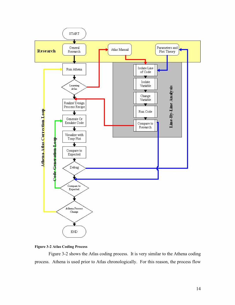
Figure 3-2 Atlas Coding Process
Figure 3-2 shows the Atlas coding process. It is very similar to the Athena coding
process. Athena is used prior to Atlas chronologically. For this reason, the process flow
15
is different. The two applications are intertwined and jumping back and forth between
the two is common for simulating wafer fabrication.
The same general research and background is applied to learning Atlas. Prior to
running Atlas code, the user must have a working Athena sample of code. Then the user
can run Atlas and begin understanding it.
Once again the user must familiarize himself with the Silvaco manual (Atlas this
time). Then the user must start with the line-by-line analysis of a piece of sample Atlas
code. Once he fully understands the code, he must reverse engineer and make a recipe of
the sample, and begin generating code.
The visualizing, and comparing steps are the same as before, as is the debugging
step. Even if the Atlas code is correct, there still may be problems with the simulation. If
this is the case, then the user will have to check the Athena code again, and start the
entire process over again.
3.2.2. Research
The same general background research will be necessary for Atlas as it was for
Athena.
The most important things to know when coding with Atlas are equations. The
user needs to know how variables are affected (inversely proportional, proportional etc.)
by the code lines. He needs to know which equations are pertinent and which ones are
being modeled in the simulation process.
The user must also understand the application of the device being fabricated (is it
depletion, inversion etc.). It may affect the atlas code, and Athena in turn.
The user must also understand the numerous plots. Specifically the user must
know IV curves, capacitance curves, bias vs conductivity, and Gummel plots. All of
these curves are useful to know about prior to coding with Atlas.
16
3.3. Deviance from Ideal Simulation Examples
3.3.1. Mesh Lines
Mesh lines are important for modeling devices and extracting their parameters.
Where mesh lines intersect, calculations occur. Important plots are based on hundreds
and sometimes thousands of these intersecting lines.
When using Athena and simulating the fabrication process, the user needs to
specify an initial mesh density. This is important because setting too many mesh points
can create long calculation times, and setting too few can cause gaps in analysis (which
may end up taking a lot of time in the long run). Typically, more mesh points occur in
the channel region and along the surface of the device. The other points are then
graduated to a lesser mesh density.
Whenever a new layer is deposited using Athena, a new mesh density must be
added. This is because no mesh lines have been specified other than the original mesh.
An entirely new layer is void of mesh formatting.
Calculation time can be reduced by using the “mirror” command within Athena.
This allows the user to only have to make half as many calculations up until the point of
mirroring. This is because there are half as many mesh calculation points. However, at
times the user may encounter devices that are a-symmetrical and are not able to be
mirrored. When that is the case, no time can be saved with the mirror command.
3.3.2. Oxidation
Growing oxides is an important step in the fabrication process. However, they
grow in very specific ways. Certain processes can be undergone in order to manipulate
the oxidation growth process, as talked about in chapter 2.
The oxide grows noticeable slower and thicker in a dry environment. In the wet
environment, it tends to grow faster. Be careful when annealing oxides numerous times
after being grown in a particular environment. It may negatively affect the outcome of
the desired oxide shape and position.
17
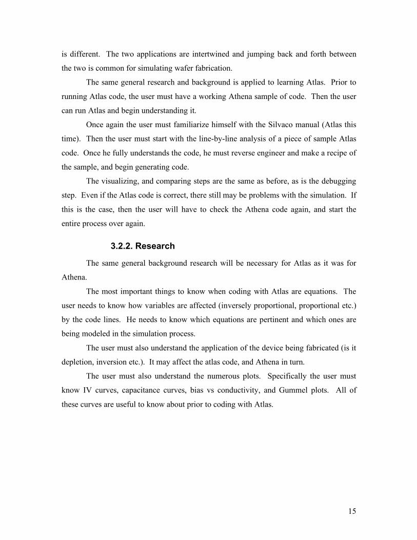
Figure 3-3 Rounded Oxide
Note how the Oxide grows with round edges in figure 3-3. This may adversely
affect results if left unanticipated. Such a scenario may exist when performing LOCOS
isolation. The user will want the oxide to grow a certain depth and width, however the
rounded edges may cut the isolation area just short of the desired area.
Oxides can also be used to shield implantations of dopants. This will be
discussed further in the masking section.
18
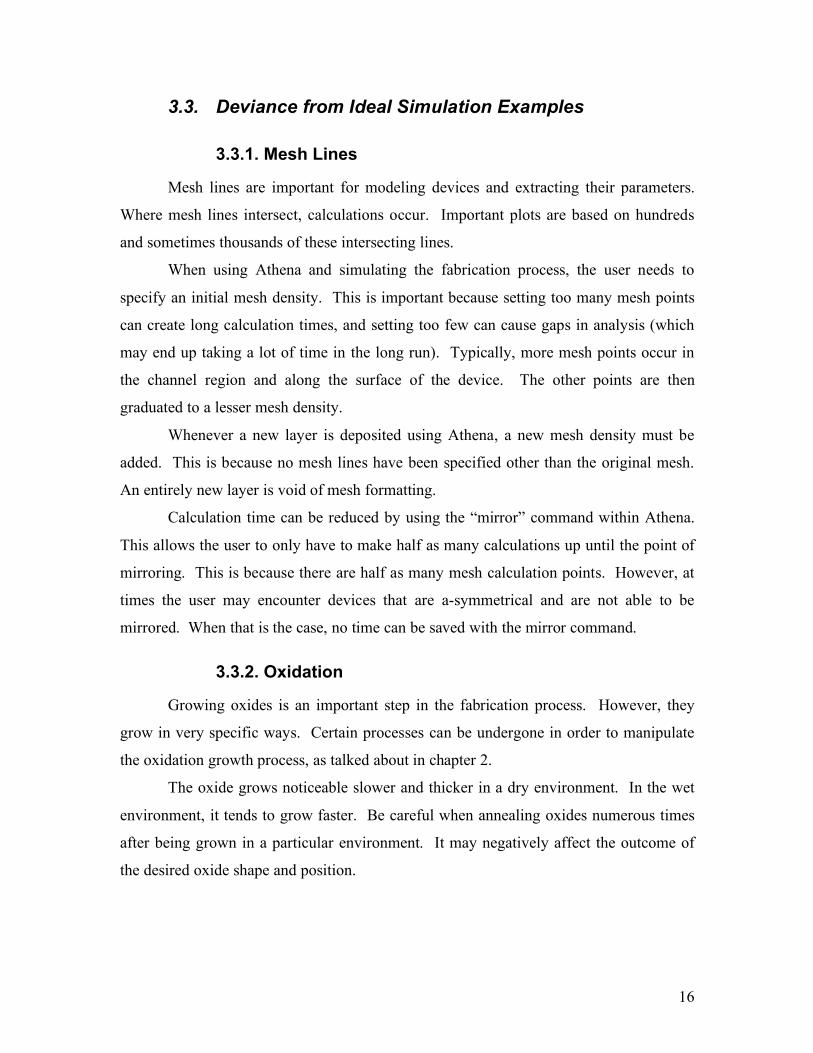
Figure 3-4 Bird Beak Effect
Figure 3-4 shows a picture of the bird beak effect. The uneven growth occurs
when growing oxides in a wet atmosphere. This problem can be facilitated by growing
the oxide in a nitrogen atmosphere. The picture above is grown in a nitrogen atmosphere.
The bird beak effect could be far more significant. Also note that Oxides grow in a 45%-
55% pattern. This is particular important when growing FOX or LOCOS isolation
oxides. 55% of the oxide is below the surface and 45% of the oxide is above the surface.
It is possible to grow the oxide too thick because of the unanticipated 55% growth below
the surface.
3.3.3. Masking
Masking is a crucial part in the fabrication process. Here masking is simulated
and depicted showing Tonyplots of Athena. It is important to specify the exact co-
ordinates of the mask layer to ensure the proper placement of the new layer being created.
19
Figure 3-5 Nitride Mask Layer
Figure 3-5 shows a nitride mask layer. This will act as a photo-resist. Oxide will
later be grown over the entire area, and later etched away.
Figure 3-6 After Nitride Mask Layer
Figure 3-6 shows the oxide grown after the nitride mask layer has been produced
and etched away. Note how the oxide has grown underneath where the nitride mask layer
20
was. This is important to note because it can effect placement of shielding oxides later
used to place a channel of dopants. It can shrink the later diffusion of the dopants.
Figure 3-7 Implantation During Mask Step
Figure 3-7 shows boron being implanted during a masking step. Note how the
diffusion pushes the surface concentration horizontally as well as vertically. It is
important to make sure to take these into account when positioning the mask layer.
3.3.4. LOCOS Isolation process
The initial project goal focused on the isolated creation of a BCD Wafer.
However, BCD fabrication adds an additional layer of complexity to the fabrication of
devices, because each component needs to be isolated from the surrounding devices.
Because of this, it was decided that LOCOS isolation be implemented into transistor
fabrication process. The following steps detail the implementation of LOCOS isolation.
a) Process Flow Insertion
The initial decision when implementing LOCOS isolation is deciding where, in
the existing process flow, the oxide layer will be grown. Through careful examination of
21
the process presented by McClay13, it was decided that the oxide layer be grown
immediately after the epitaxial layer growth. The reason for this is that there are
significant annealing steps that occur in order to grow the oxide to the desired depth and
thickness. Were this process to be delayed until after the implantation of either the
source/drain or channel dopants, then the diffusion depths and characteristics of any
dopants would change dramatically. By performing the LOCOS process first, we were
able to maintain the same process flow for the remainder of the device.
b) Barrier Layers, Silicon Etching, and Oxide
Growth
As discussed earlier, when a layer of oxide is grown on top of silicon, it results in
a slightly uneven dispersion of the oxide. This 55/45 (above/below) growth ratio will
need to be taken into consideration so that the silicon is etched to the right depth before
the wafer is annealed. However, before the silicon is etched, several layers are placed on
top of the wafer, in order to protect those parts of the device that the designer wished to
remain unchanged.
These layers consist of a thin layer of oxide (.01µm), a thick layer of nitride
(.3µm) and a barrier layer (.1µm). All of these layers serve to protect the silicon,
however the nitride serves an additional purpose. The nitride layer is especially thick,
because it helps inhibit the “bird beak” effect. This negative effect of oxide growth will
cause the oxide to spread horizontally into the device. Once the barriers are in place, and
the silicon etched, the device will resemble that of figure 3-8.
13 McClay
22
Figure 3-8 Silicon Wafer post Etching
Figure 3-8 shows the nitride layer and the barrier layer on top of the silicon wafer.
c) Oxide Growth and Final Device Geometry
The device is now annealed in a water vapor environment, at a temperature of
1200oC for a time of 60 minutes. According to figure 4-1, this should yield an oxide
thickness of close to 1µm. Whether or not this is deep enough can only be determined
once the device is completed, and the pn junction lines, as well as current flow can be
modeled and examined. For now, the device looks like that of figure 3-9.
23
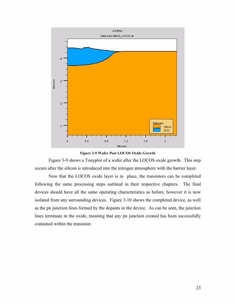
Figure 3-9 Wafer Post LOCOS Oxide Growth
Figure 3-9 shows a Tonyplot of a wafer after the LOCOS oxide growth. This step
occurs after the silicon is introduced into the nitrogen atmosphere with the barrier layer.
Now that the LOCOS oxide layer is in place, the transistors can be completed
following the same processing steps outlined in their respective chapters. The final
devices should have all the same operating characteristics as before, however it is now
isolated from any surrounding devices. Figure 3-10 shows the completed device, as well
as the pn junction lines formed by the dopants in the device. As can be seen, the junction
lines terminate in the oxide, meaning that any pn junction created has been successfully
contained within the transistor.
24
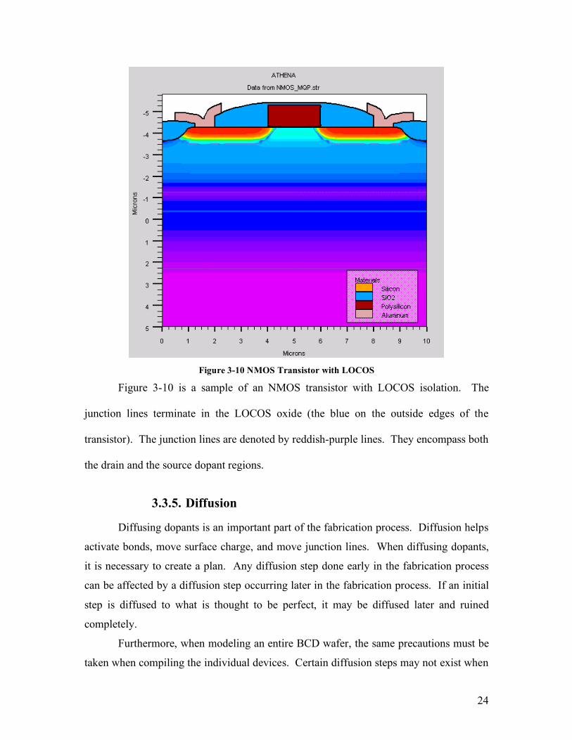
Figure 3-10 NMOS Transistor with LOCOS
Figure 3-10 is a sample of an NMOS transistor with LOCOS isolation. The
junction lines terminate in the LOCOS oxide (the blue on the outside edges of the
transistor). The junction lines are denoted by reddish-purple lines. They encompass both
the drain and the source dopant regions.
3.3.5. Diffusion
Diffusing dopants is an important part of the fabrication process. Diffusion helps
activate bonds, move surface charge, and move junction lines. When diffusing dopants,
it is necessary to create a plan. Any diffusion step done early in the fabrication process
can be affected by a diffusion step occurring later in the fabrication process. If an initial
step is diffused to what is thought to be perfect, it may be diffused later and ruined
completely.
Furthermore, when modeling an entire BCD wafer, the same precautions must be
taken when compiling the individual devices. Certain diffusion steps may not exist when
25
modeling the individual devices. But when putting them all together, they may be
additional diffusion steps that may affect the individual devices.
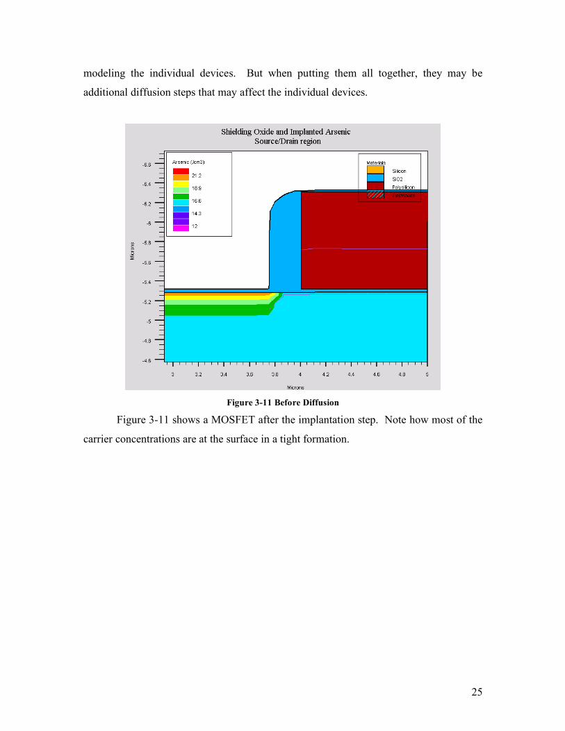
Figure 3-11 Before Diffusion
Figure 3-11 shows a MOSFET after the implantation step. Note how most of the
carrier concentrations are at the surface in a tight formation.
26
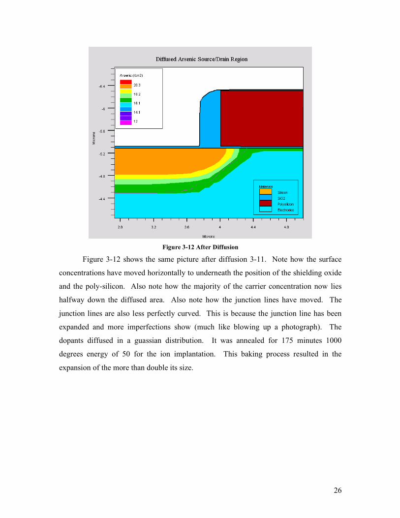
Figure 3-12 After Diffusion
Figure 3-12 shows the same picture after diffusion 3-11. Note how the surface
concentrations have moved horizontally to underneath the position of the shielding oxide
and the poly-silicon. Also note how the majority of the carrier concentration now lies
halfway down the diffused area. Also note how the junction lines have moved. The
junction lines are also less perfectly curved. This is because the junction line has been
expanded and more imperfections show (much like blowing up a photograph). The
dopants diffused in a guassian distribution. It was annealed for 175 minutes 1000
degrees energy of 50 for the ion implantation. This baking process resulted in the
expansion of the more than double its size.
27
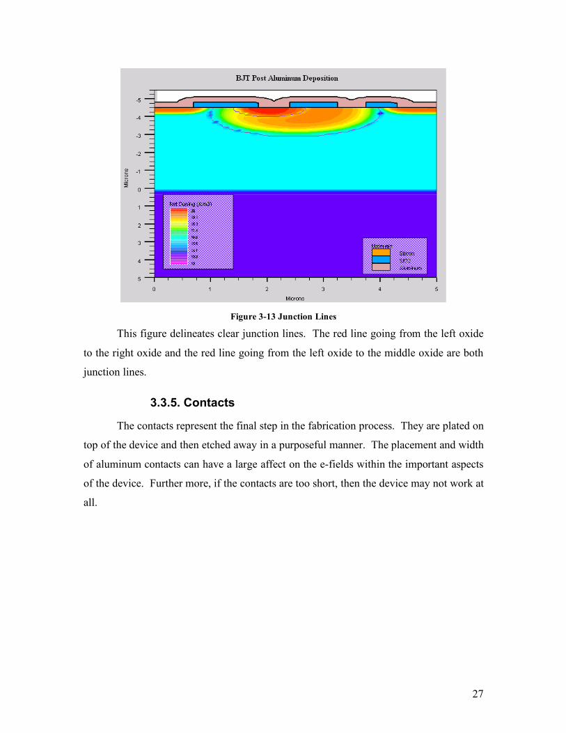
Figure 3-13 Junction Lines
This figure delineates clear junction lines. The red line going from the left oxide
to the right oxide and the red line going from the left oxide to the middle oxide are both
junction lines.
3.3.5. Contacts
The contacts represent the final step in the fabrication process. They are plated on
top of the device and then etched away in a purposeful manner. The placement and width
of aluminum contacts can have a large affect on the e-fields within the important aspects
of the device. Further more, if the contacts are too short, then the device may not work at
all.
28
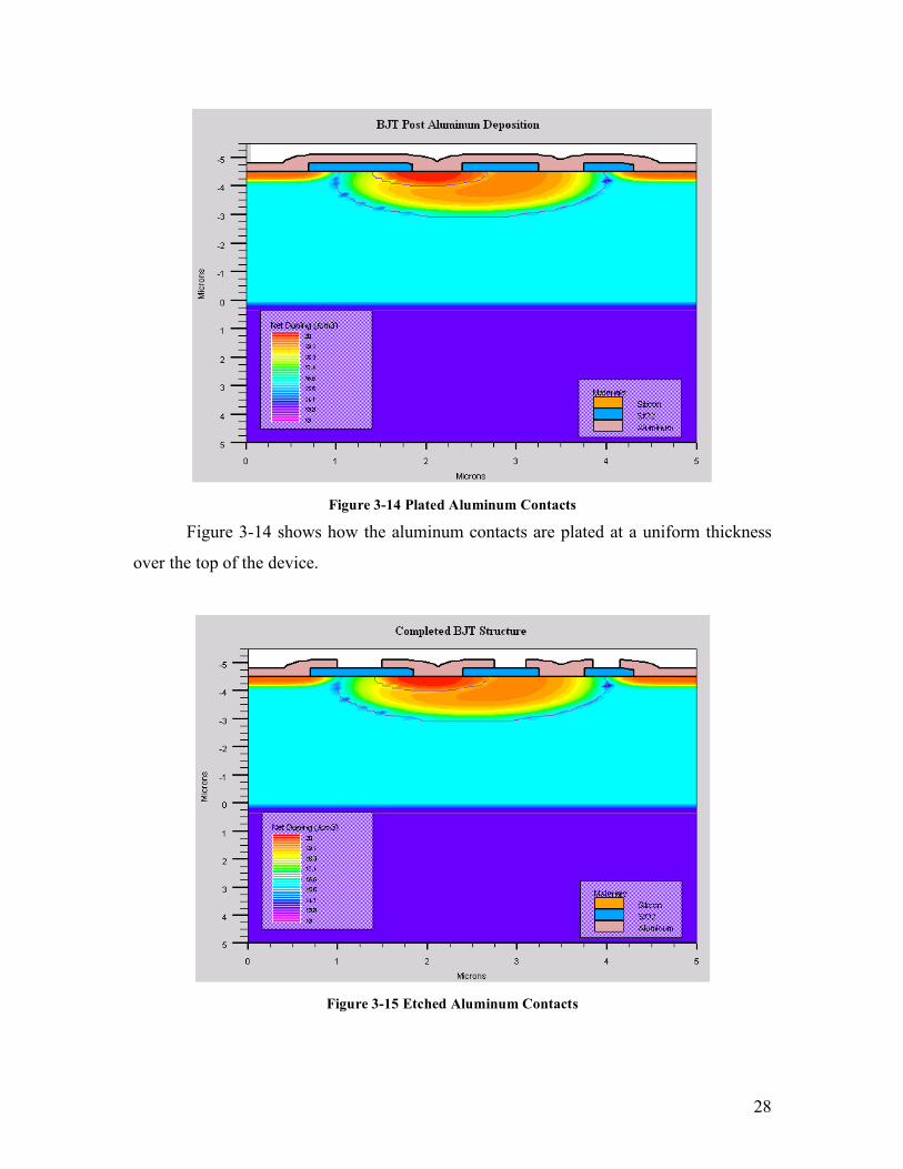
Figure 3-14 Plated Aluminum Contacts
Figure 3-14 shows how the aluminum contacts are plated at a uniform thickness
over the top of the device.
Figure 3-15 Etched Aluminum Contacts
29
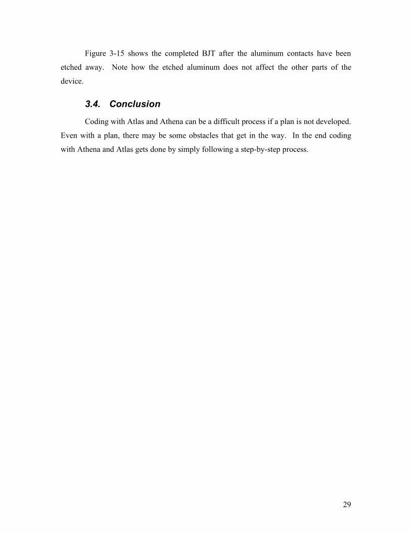
Figure 3-15 shows the completed BJT after the aluminum contacts have been
etched away. Note how the etched aluminum does not affect the other parts of the
device.
3.4. Conclusion
Coding with Atlas and Athena can be a difficult process if a plan is not developed.
Even with a plan, there may be some obstacles that get in the way. In the end coding
with Athena and Atlas gets done by simply following a step-by-step process.
30
4. CMOS Transistor The first phase of our project was to familiarize ourselves with the Silvaco
software by analyzing and adapting an existing Atlas example of an NMOS transistor. By
using an existing example, we were able to dissect functional code, and hopefully, rapidly
increase our knowledge of how to use Silvaco for device modeling. Single changes could
be made to the code, and their effects could be immediately seen through the output
graphs. This allowed us to better understand the processing steps of creating a CMOS
device, and in a much shorter amount of time than had we started with no example code.
Additionally, the reason a CMOS device was chosen as the first BCD device we
would create was for its relative simplicity compared to an LDMOS transistor, as well as
our current level of familiarity with CMOS transistors. This chapter is introduced by a
concise problem statement, and then the theoretical performance characteristics. Then, a
detailed process for the development of an NMOS transistor is presented. LOCOS
isolation is then examined through its addition to the NMOS fabrication process. Lastly,
the Atlas generated results are compared to the theoretical behavior as described in
section 3.2.
4.1. Problem Statement
Our first goal was to modify the code so that the device would be scaled up to
closer reflect the size of a BCD-III transistor. The NMOS transistor supplied in the Atlas
example measured 1.2µm wide by .8µm tall and had a gate oxide thickness of
approximately .01µm. As Silvaco does not render devices in three dimensions, it is not
possible to declare the desired width of the device. Rather, results that are dependant
upon the width of the transistor are given as “per unit width”, typically per micrometer.
Once the physical size of the device was modified, it would then be our goal to change
enough of the processing steps, like ion implantation energy, diffusion lengths, oxide
thicknesses, etc., until we achieved a transistor that exhibited real world operating
characteristics. Both an NMOS and a PMOS transistor were to be attempted during the
first stage of our project.
31
4.2. Theoretical Device Characteristics
In addition to the physical parameters taken from Jim McClay’s14 research, it was
important that we establish which family of BCD devices our transistor would belong to.
After some thought, it was decided that the BCD-III family would be a good fit for our
purposes, as it was physically large enough that issues such as sheet resistance and
parasitic capacitances would not play a large adverse role in the functionality of our
finished transistor.
Additionally, in order to obtain these characteristics, we spent time during our
research focusing on the key equations and charts for parameters such as the threshold
voltage, I-V curves, diffusion depths, and oxide thickness. This information would allow
us to intelligently manipulate the Atlas example, and analyze our results to notice any
deviancy from the ideal.
4.2.1. Oxide Thickness
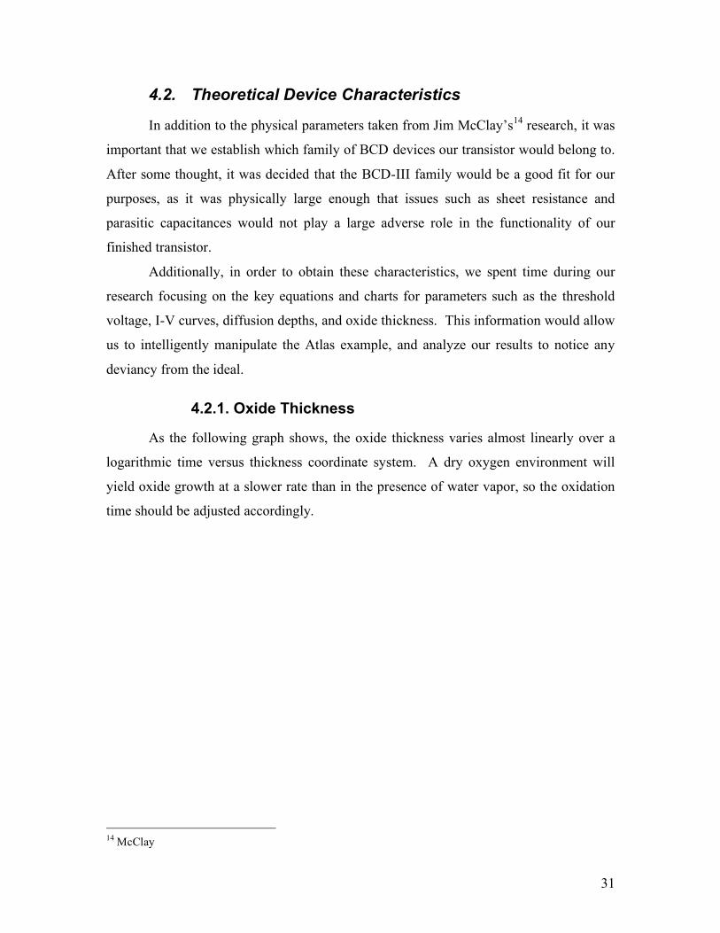
As the following graph shows, the oxide thickness varies almost linearly over a
logarithmic time versus thickness coordinate system. A dry oxygen environment will
yield oxide growth at a slower rate than in the presence of water vapor, so the oxidation
time should be adjusted accordingly.
14 McClay
32
Figure 4-1: Oxidation thickness versus time for wet and dry O2
Figure 4-1 shows an oxidation thickness versus time for annealing oxide in both a
wet and dry process. Note where the dotted line of the 1000 oC line meets with the
annealing time of 12 minutes.15
The BCD-III requirement of a 28 nm gate oxide means that if we were to use a
dry oxygen environment, at a temperature of 1000 oC, then we would need to let the
oxide grow for a total time of approximately 12 minutes.
4.2.2. Threshold Voltage
Having the correct gate oxide thickness is crucial, because it plays the largest role
in the determination of the transistor’s turn-on voltage. The capacitance induced by the
gate oxide is what largely determines the amount of charge needed at the gate, in order to
create the conductive channel to connect the drain and source. The equations controlling
this behavior are:
!!"
#$$%
&'=
i
Df
n
N
q
kTln( Equation 1
15 Introduction to Microelectronic Fabrication pg 34.
33
)(4
20
F
S
D
O
oS
FTK
qN
K
xKV !
"! ##= Equation 2
Where F!2 =
S! = energy required for channel inversion
Description Symbol Value
Thermal voltage
@ T = 300K q
kT .0259 V
dielectric constant of Si KS 11.9
dielectric constant of SiO2 KO 3.9
gate oxide thickness x0 28nm
donor concentration at surface
of silicon
ND 1 x 10¹⁸
intrinsic carrier concentration Ni 1 x 10¹⁰
permittivity of free space ε0 8.85 x 10⁻¹⁴ Table 4-1: Threshold Voltage Symbol Explanation
Table 4-1 explains the first two equations.
Based on these equations, if our final device has the same doping characteristics,
than the turn-on voltage should be approximately .91 volts. In order to achieve this
value, we must be careful to properly dope the source and drain regions so that the donor
concentration is as close to 1 x 10¹⁸/cm3 as possible. These regions are shown in figure
3-3, on page14. Then, once the device is simulated, and the turn-on voltage observed,
adjustments can be made.
4.2.3. I-V Characteristics
When fabricating a CMOS device, the drain current versus drain voltage
relationship is an essential consideration. By fixing the gate voltage at separate voltage
levels, and then swinging the drain voltage over a range of values, the drain current
should increase asymptotically up to its saturation limit, IDsat. IDsat occurs when the drain
voltage equals its saturation level, VDsat = VG - VT, and is given by the equation:
20 )(2
TG
n
DsatVV
L
CZI !=
µ Equation 3
34
Description Symbol
Saturation Current DsatI
Effective Carrier
Mobility n
µ
Capacitance per unit
Area of the gate 0C
Channel Width Z
Channel Length L
Threshold Voltage TV
Gate Voltage GV
Table 4-2: Saturation Current Symbol Explanation
Table 4-2 explains the variable entailed in equation 3.
Ideally, this value would remain constant as VD exceeds VDsat. However, due to
device non-idealities, such as leakage current from the drain to the body, the actual drain
current will slightly exceed the predicted saturation current for larger values of drain
voltage, VD > VDsat.
Additionally, for digital switching applications, designers would prefer that the
increase in drain current vary linearly with the increase in gate voltage applied. That
way, the drain voltage could be held constant, and the current varied linearly with the
gate voltage. However, for long channel devices such as this, the behavior of the drain
current is governed by the square law, 2)(TGVV ! , and therefore this request cannot be
met.16
4.3. Walkthrough of CMOS Fabrication
Now that the main operating characteristics of the CMOS device have been
established it is time to use Silvaco to fabricate a device with operating characteristics as
close to these as possible. Additionally, Silvaco will reveal to us how the device should
actually behave, and we will be able to use these results and compare its actual operation,
16 Analog Integrated Circuit Design
35
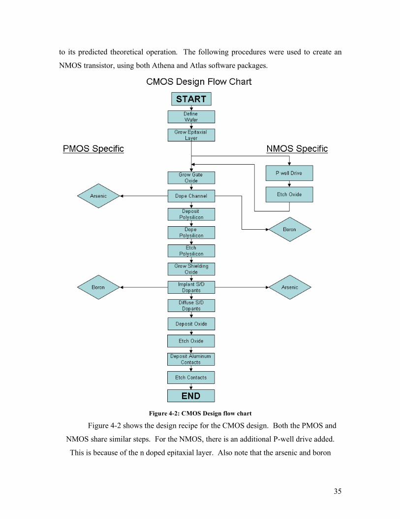
to its predicted theoretical operation. The following procedures were used to create an
NMOS transistor, using both Athena and Atlas software packages.
Figure 4-2: CMOS Design flow chart
Figure 4-2 shows the design recipe for the CMOS design. Both the PMOS and
NMOS share similar steps. For the NMOS, there is an additional P-well drive added.
This is because of the n doped epitaxial layer. Also note that the arsenic and boron
36
doping stages of the NMOS and PMOS are switched. This is because each has a
differently doped channel, and the other steps interfere with the order of processing steps.
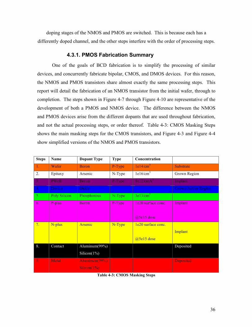
4.3.1. PMOS Fabrication Summary
One of the goals of BCD fabrication is to simplify the processing of similar
devices, and concurrently fabricate bipolar, CMOS, and DMOS devices. For this reason,
the NMOS and PMOS transistors share almost exactly the same processing steps. This
report will detail the fabrication of an NMOS transistor from the initial wafer, through to
completion. The steps shown in Figure 4-7 through Figure 4-10 are representative of the
development of both a PMOS and NMOS device. The difference between the NMOS
and PMOS devices arise from the different dopants that are used throughout fabrication,
and not the actual processing steps, or order thereof. Table 4-3: CMOS Masking Steps
shows the main masking steps for the CMOS transistors, and Figure 4-3 and Figure 4-4
show simplified versions of the NMOS and PMOS transistors.
Steps Name Dopant Type Type Concentration
1. Wafer Boron P-Type 1e14/cm3 Substrate
2. Epitaxy Arsenic N-Type 1e16/cm3 Grown Region
3. PWell Boron P-Type 8e12/cmA3 Implant
4. Device Oxide Grown/Active Region
5. Poly Silicon Phosphorous N-Type 3e13/cm3
6. P-plus Boron P-Type 1e20 surface conc.
@5e15 dose
Implant
7. N-plus Arsenic N-Type 1e20 surface conc.
@5e15 dose
Implant
8. Contact Aluminum(99%)
Silicon(1%)
Deposited
9. Metal Aluminum(99%)
Silicon(1%)
Deposited
Table 4-3: CMOS Masking Steps
37
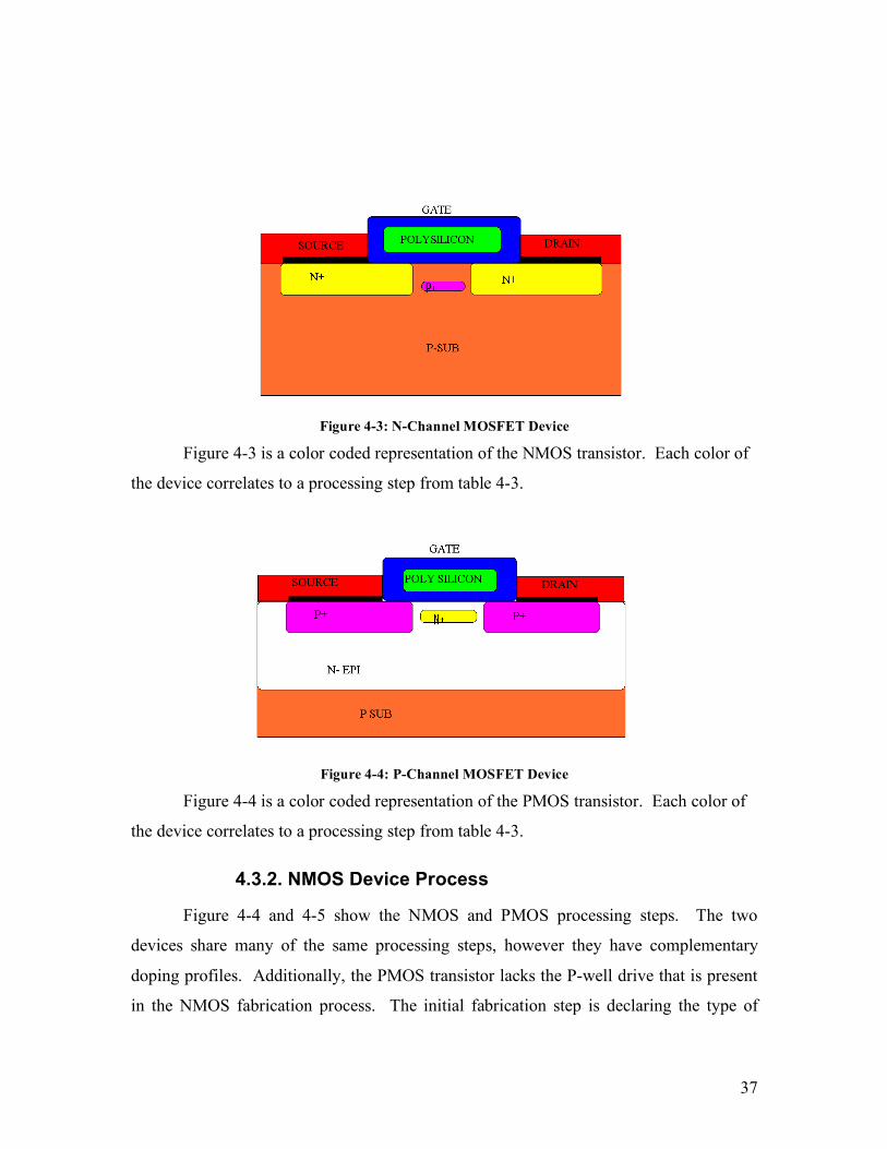
Figure 4-3: N-Channel MOSFET Device
Figure 4-3 is a color coded representation of the NMOS transistor. Each color of
the device correlates to a processing step from table 4-3.
Figure 4-4: P-Channel MOSFET Device
Figure 4-4 is a color coded representation of the PMOS transistor. Each color of
the device correlates to a processing step from table 4-3.
4.3.2. NMOS Device Process
Figure 4-4 and 4-5 show the NMOS and PMOS processing steps. The two
devices share many of the same processing steps, however they have complementary
doping profiles. Additionally, the PMOS transistor lacks the P-well drive that is present
in the NMOS fabrication process. The initial fabrication step is declaring the type of
38
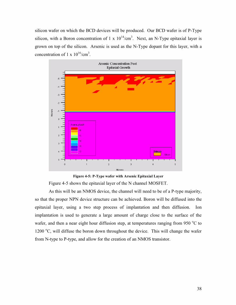
silicon wafer on which the BCD devices will be produced. Our BCD wafer is of P-Type
silicon, with a Boron concentration of 1 x 10¹⁴/cm3. Next, an N-Type epitaxial layer is
grown on top of the silicon. Arsenic is used as the N-Type dopant for this layer, with a
concentration of 1 x 10¹⁶/cm3.
Figure 4-5: P-Type wafer with Arsenic Epitaxial Layer
Figure 4-5 shows the epitaxial layer of the N channel MOSFET.
As this will be an NMOS device, the channel will need to be of a P-type majority,
so that the proper NPN device structure can be achieved. Boron will be diffused into the
epitaxial layer, using a two step process of implantation and then diffusion. Ion
implantation is used to generate a large amount of charge close to the surface of the
wafer, and then a near eight hour diffusion step, at temperatures ranging from 950 oC to
1200 oC, will diffuse the boron down throughout the device. This will change the wafer
from N-type to P-type, and allow for the creation of an NMOS transistor.
39
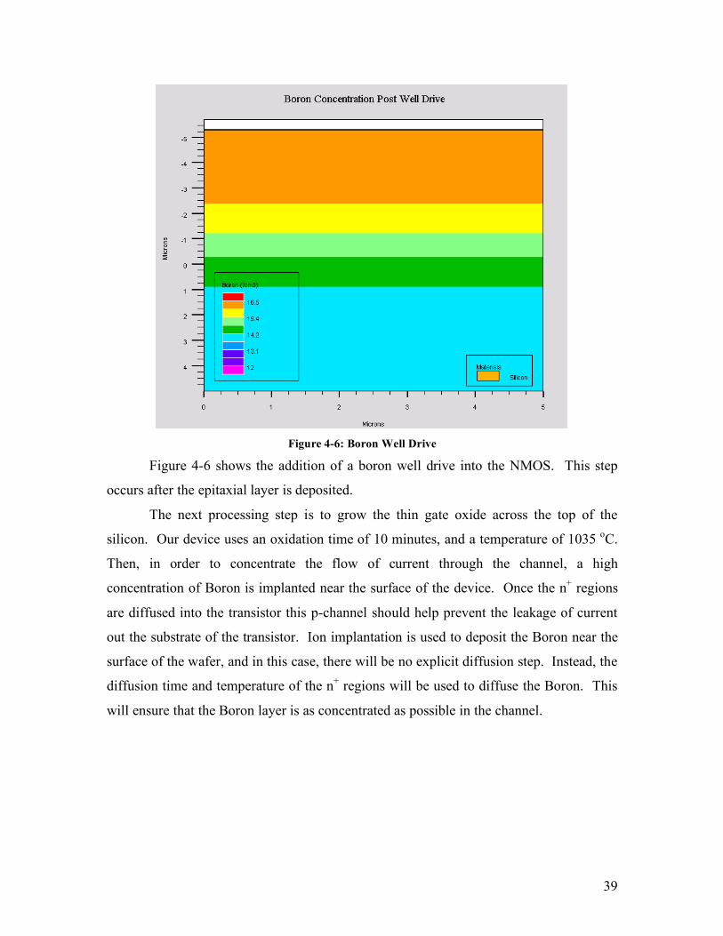
Figure 4-6: Boron Well Drive
Figure 4-6 shows the addition of a boron well drive into the NMOS. This step
occurs after the epitaxial layer is deposited.
The next processing step is to grow the thin gate oxide across the top of the
silicon. Our device uses an oxidation time of 10 minutes, and a temperature of 1035 oC.
Then, in order to concentrate the flow of current through the channel, a high
concentration of Boron is implanted near the surface of the device. Once the n+ regions
are diffused into the transistor this p-channel should help prevent the leakage of current
out the substrate of the transistor. Ion implantation is used to deposit the Boron near the
surface of the wafer, and in this case, there will be no explicit diffusion step. Instead, the
diffusion time and temperature of the n+ regions will be used to diffuse the Boron. This
will ensure that the Boron layer is as concentrated as possible in the channel.
40
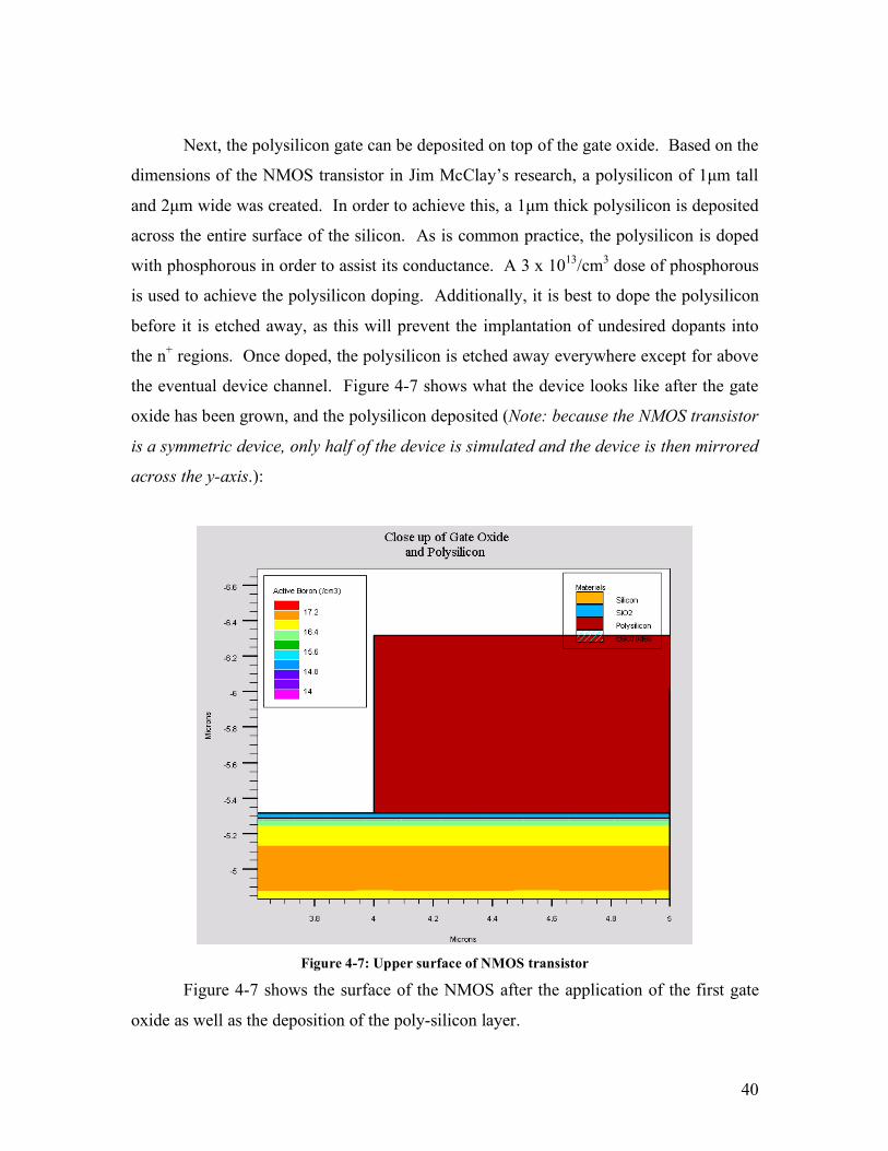
Next, the polysilicon gate can be deposited on top of the gate oxide. Based on the
dimensions of the NMOS transistor in Jim McClay’s research, a polysilicon of 1µm tall
and 2µm wide was created. In order to achieve this, a 1µm thick polysilicon is deposited
across the entire surface of the silicon. As is common practice, the polysilicon is doped
with phosphorous in order to assist its conductance. A 3 x 10¹³/cm3 dose of phosphorous
is used to achieve the polysilicon doping. Additionally, it is best to dope the polysilicon
before it is etched away, as this will prevent the implantation of undesired dopants into
the n+ regions. Once doped, the polysilicon is etched away everywhere except for above
the eventual device channel. Figure 4-7 shows what the device looks like after the gate
oxide has been grown, and the polysilicon deposited (Note: because the NMOS transistor
is a symmetric device, only half of the device is simulated and the device is then mirrored
across the y-axis.):
Figure 4-7: Upper surface of NMOS transistor
Figure 4-7 shows the surface of the NMOS after the application of the first gate
oxide as well as the deposition of the poly-silicon layer.
41
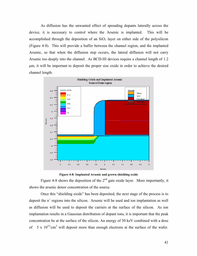
As diffusion has the unwanted effect of spreading dopants laterally across the
device, it is necessary to control where the Arsenic is implanted. This will be
accomplished through the deposition of an SiO2 layer on either side of the polysilicon
(Figure 4-8). This will provide a buffer between the channel region, and the implanted
Arsenic, so that when the diffusion step occurs, the lateral diffusion will not carry
Arsenic too deeply into the channel. As BCD-III devices require a channel length of 1.2
µm, it will be important to deposit the proper size oxide in order to achieve the desired
channel length.
Figure 4-8: Implanted Arsenic and grown shielding oxide
Figure 4-8 shows the deposition of the 2nd gate oxide layer. More importantly, it
shows the arsenic donor concentration of the source.
Once this “shielding oxide” has been deposited, the next stage of the process is to
deposit the n+ regions into the silicon. Arsenic will be used and ion implantation as well
as diffusion will be used to deposit the carriers at the surface of the silicon. As ion
implantation results in a Gaussian distribution of dopant ions, it is important that the peak
concentration be at the surface of the silicon. An energy of 50 keV combined with a dose
of 5 x 10¹⁵/cm3 will deposit more than enough electrons at the surface of the wafer.
42
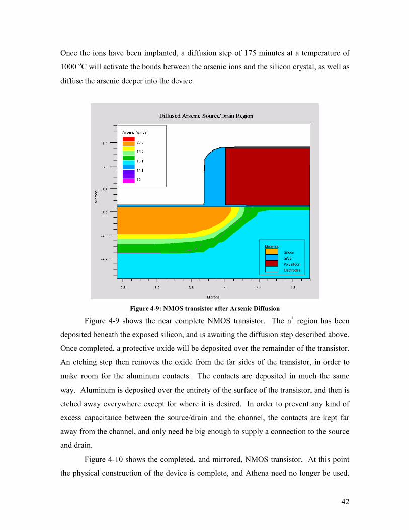
Once the ions have been implanted, a diffusion step of 175 minutes at a temperature of
1000 oC will activate the bonds between the arsenic ions and the silicon crystal, as well as
diffuse the arsenic deeper into the device.
Figure 4-9: NMOS transistor after Arsenic Diffusion
Figure 4-9 shows the near complete NMOS transistor. The n+ region has been
deposited beneath the exposed silicon, and is awaiting the diffusion step described above.
Once completed, a protective oxide will be deposited over the remainder of the transistor.
An etching step then removes the oxide from the far sides of the transistor, in order to
make room for the aluminum contacts. The contacts are deposited in much the same
way. Aluminum is deposited over the entirety of the surface of the transistor, and then is
etched away everywhere except for where it is desired. In order to prevent any kind of
excess capacitance between the source/drain and the channel, the contacts are kept far
away from the channel, and only need be big enough to supply a connection to the source
and drain.
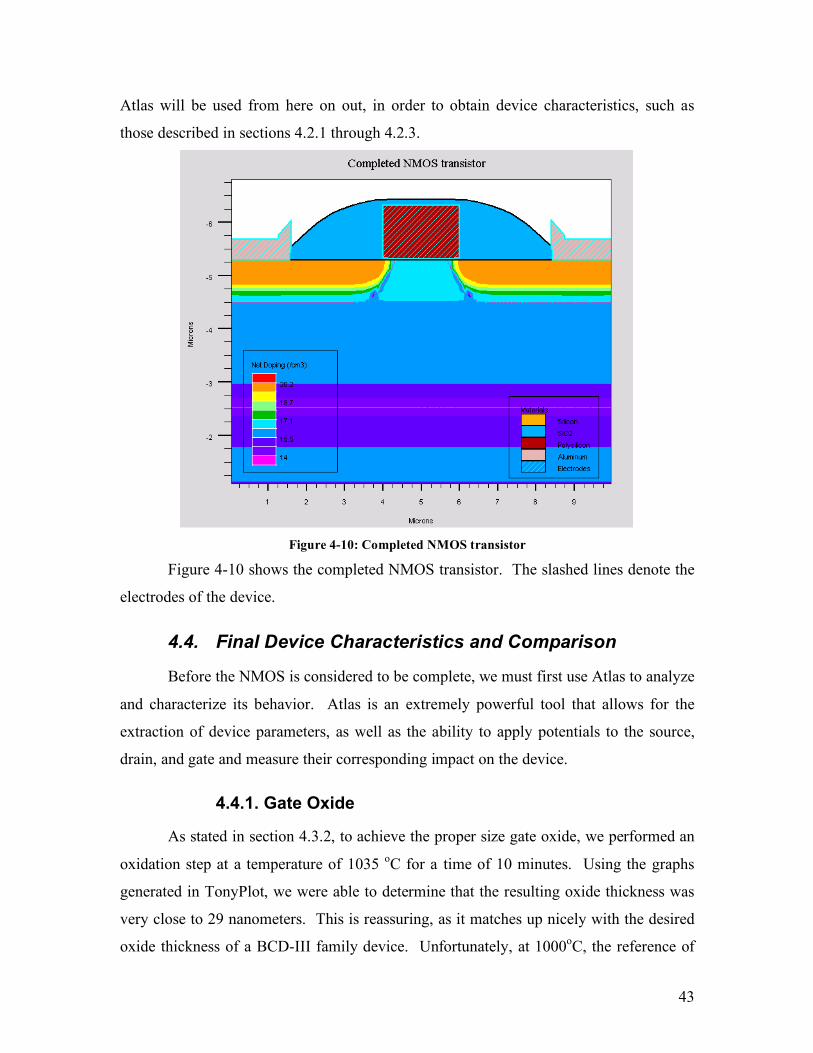
Figure 4-10 shows the completed, and mirrored, NMOS transistor. At this point
the physical construction of the device is complete, and Athena need no longer be used.
43
Atlas will be used from here on out, in order to obtain device characteristics, such as
those described in sections 4.2.1 through 4.2.3.
Figure 4-10: Completed NMOS transistor
Figure 4-10 shows the completed NMOS transistor. The slashed lines denote the
electrodes of the device.
4.4. Final Device Characteristics and Comparison
Before the NMOS is considered to be complete, we must first use Atlas to analyze
and characterize its behavior. Atlas is an extremely powerful tool that allows for the
extraction of device parameters, as well as the ability to apply potentials to the source,
drain, and gate and measure their corresponding impact on the device.
4.4.1. Gate Oxide
As stated in section 4.3.2, to achieve the proper size gate oxide, we performed an
oxidation step at a temperature of 1035 oC for a time of 10 minutes. Using the graphs
generated in TonyPlot, we were able to determine that the resulting oxide thickness was
very close to 29 nanometers. This is reassuring, as it matches up nicely with the desired
oxide thickness of a BCD-III family device. Unfortunately, at 1000oC, the reference of
44
Figure 4-1: Oxidation thickness versus time for wet and dry O2, does not provide a
defined line for an annealing time of 10 minutes. However, by extrapolating, it can be
determined that the predicted oxide thickness should be approximately 30-35 nm.17 This
value correlates quite nicely with the value we obtained through the Athena simulation
software.
4.4.2. Threshold Voltage
In order to establish what the turn-on voltage of the transistor is, the gate bias
versus conductivity was plotted. Based on the graph it was possible to determine at
which voltage the transistor would turn on, and begin conducting current. Figure 4-11
shows the conductivity versus bias relationship that we attained with the device, and it
can be determined that the transistor will turn on at approximately .8 V. More
specifically, equations 1 and 2 can be used to calculate the predicted turn-on voltage.
Our final device had n+ regions doped with a donor concentration of
approximately 1 x 10²⁰/cm3 near the surface of the wafer. Additionally, our oxide
thickness is 29 nm. By plugging these numbers into the two equations, we get a
predicted turn-on voltage of .8 volts. This number is very close to our graphical
approximation, and that similarity is encouraging to see.
17 Introduction to Microelectronic Fabrication pg. 34
45
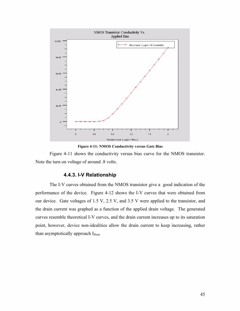
Figure 4-11: NMOS Conductivity versus Gate Bias
Figure 4-11 shows the conductivity versus bias curve for the NMOS transistor.
Note the turn on voltage of around .8 volts.
4.4.3. I-V Relationship
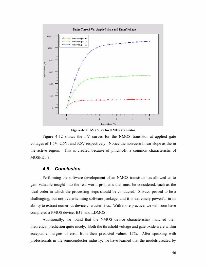
The I-V curves obtained from the NMOS transistor give a good indication of the
performance of the device. Figure 4-12 shows the I-V curves that were obtained from
our device. Gate voltages of 1.5 V, 2.5 V, and 3.5 V were applied to the transistor, and
the drain current was graphed as a function of the applied drain voltage. The generated
curves resemble theoretical I-V curves, and the drain current increases up to its saturation
point, however, device non-idealities allow the drain current to keep increasing, rather
than asymptotically approach IDsat.
46
Figure 4-12: I-V Curve for NMOS transistor
Figure 4-12 shows the I-V curves for the NMOS transistor at applied gate
voltages of 1.5V, 2.5V, and 3.5V respectively. Notice the non-zero linear slope as the in
the active region. This is created because of pinch-off, a common characteristic of
MOSFET’s.
4.5. Conclusion
Performing the software development of an NMOS transistor has allowed us to
gain valuable insight into the real world problems that must be considered, such as the
ideal order in which the processing steps should be conducted. Silvaco proved to be a
challenging, but not overwhelming software package, and it is extremely powerful in its
ability to extract numerous device characteristics. With more practice, we will soon have
completed a PMOS device, BJT, and LDMOS.
Additionally, we found that the NMOS device characteristics matched their
theoretical prediction quite nicely. Both the threshold voltage and gate oxide were within
acceptable margins of error from their predicted values, 15%. After speaking with
professionals in the semiconductor industry, we have learned that the models created by

47
Silvaco should very accurately match their physical counterparts, and it can serve to
highlight the discrepancies that arise between the theoretical and the actual.
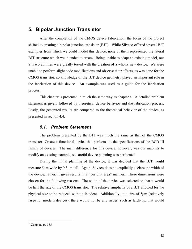
48
5. Bipolar Junction Transistor After the completion of the CMOS device fabrication, the focus of the project
shifted to creating a bipolar junction transistor (BJT). While Silvaco offered several BJT
examples from which we could model this device, none of them represented the lateral
BJT structure which we intended to create. Being unable to adapt an existing model, our
Silvaco abilities were greatly tested with the creation of a wholly new device. We were
unable to perform slight code modifications and observe their effects, as was done for the
CMOS transistor, so knowledge of the BJT device geometry played an important role in
the fabrication of this device. An example was used as a guide for the fabrication
process.18
This chapter is presented in much the same way as chapter 4. A detailed problem
statement is given, followed by theoretical device behavior and the fabrication process.
Lastly, the generated results are compared to the theoretical behavior of the device, as
presented in section 4.4.
5.1. Problem Statement
The problem presented by the BJT was much the same as that of the CMOS
transistor: Create a functional device that performs to the specifications of the BCD-III
family of devices. The main difference for this device, however, was our inability to
modify an existing example, so careful device planning was performed.
During the initial planning of the device, it was decided that the BJT would
measure 5µm wide by 9.5µm tall. Again, Silvaco does not explicitly declare the width of
the device, rather, it gives results in a “per unit area” manner. These dimensions were
chosen for the following reasons. The width of the device was selected so that it would
be half the size of the CMOS transistor. The relative simplicity of a BJT allowed for the
physical size to be reduced without incident. Additionally, at a size of 5µm (relatively
large for modern devices), there would not be any issues, such as latch-up, that would
18 Zambuto pg 335
49
need to be considered. 9.5µm represents the approximate height of the devices presented
in Jim McClay’s report.19
5.2. Theoretical Device Characteristics
Much the same as the CMOS transistor, the BJT must conform to the
characteristics of the BCD-III family of devices, as defined in Table 2-1. Additionally,
measurements such as the Gummel plot, as well as the I-V characteristics were used to
ensure that the device was working properly, with as little deviation from the theoretical
as possible. Silvaco is equipped with many different models that recreate real life device
imperfections, so their effects are observable through the simulations that are generated.
5.2.1. Gummel Plot
The Gummel plot is used to represent the “simultaneous semi log plot of IB and IC
as a function of the input voltage VEB”.20 The value of this plot is that it will showcase the
current characteristics of the BJT over a range of voltages The figure below shows a
Gummel plot with both actual and theoretical behaviors represented. Additionally, this
graph will allow the extraction of key values such as the βdc.
19 McClay 20 Pierret pg. 424
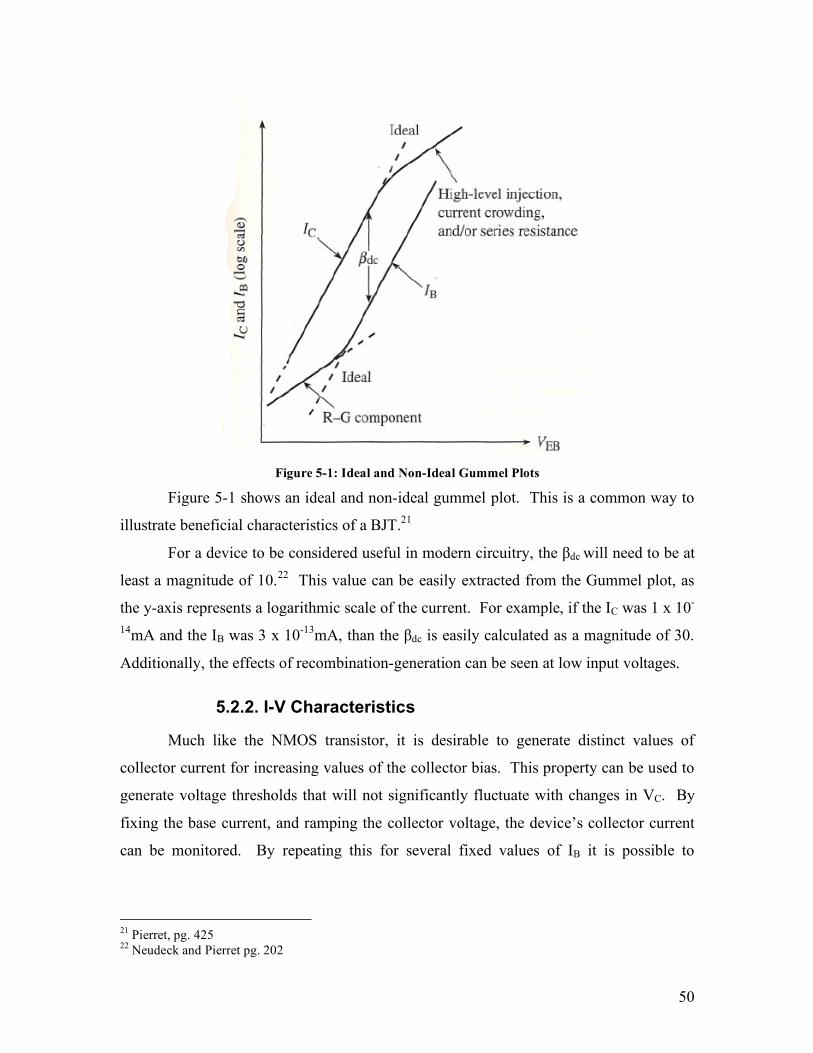
50
Figure 5-1: Ideal and Non-Ideal Gummel Plots
Figure 5-1 shows an ideal and non-ideal gummel plot. This is a common way to
illustrate beneficial characteristics of a BJT.21
For a device to be considered useful in modern circuitry, the βdc will need to be at
least a magnitude of 10.22 This value can be easily extracted from the Gummel plot, as
the y-axis represents a logarithmic scale of the current. For example, if the IC was 1 x 10-
14mA and the IB was 3 x 10-13mA, than the βdc is easily calculated as a magnitude of 30.
Additionally, the effects of recombination-generation can be seen at low input voltages.
5.2.2. I-V Characteristics
Much like the NMOS transistor, it is desirable to generate distinct values of
collector current for increasing values of the collector bias. This property can be used to
generate voltage thresholds that will not significantly fluctuate with changes in VC. By
fixing the base current, and ramping the collector voltage, the device’s collector current
can be monitored. By repeating this for several fixed values of IB it is possible to
21 Pierret, pg. 425 22 Neudeck and Pierret pg. 202
51
determine the characteristics over a wide range of values. Figure 5-2 shows a sample I-V
characteristic for a PNP transistor.
For fast switching applications, it is ideal for the collector current to ramp up to its
asymptotical limit as quickly as possible, and tradeoffs can be made for the devices
performance for increasing values of collector voltage. However, for high power
applications, it is vital that the collector current suffer only slight variations from its ideal
value as the collector voltages continue to ramp up. For the purposes of this project, we
will try to achieve a device that has good performance in both categories, however does
not necessary specialize in either. Suggestions will be made that would improve the
device’s performance for either higher power, or fast switching applications.
Figure 5-2: Sample Ideal I-V characteristics for a PNP BJT
Figure 5-2 shows the ideal I-V characteristic of a BJT (PNP). Note how the idea curve is a step function.23
5.3. Walkthrough of BJT Fabrication
While the NMOS and PMOS transistors were able to use almost the same
processing steps, the BJT requires several different processing steps, as well as the
exclusion of many of the CMOS steps. The BJT transistor does not need the application
23 Pierret pg. 408
52
of a polysilicon layer, nor does it require the growth of a gate oxide, due to the behavioral
differences of a BJT. Figure 5-3 provides a recipe for the creation of a BJT device. For
this section, we will examine the fabrication of a dedicated lateral BJT, and will delay its
integration into a full BCD process procedure until satisfactory behavior can be achieved.
Figure 5-3: BJT Process Recipe
53
Figure 5-3 shows the process recipe for the BJT. Note how the subroutine of the
implant process occurs every time a masking layer is needed to implant a concentration
of doped silicon.
Figure 5-4, below, shows a simplified version of the bipolar junction transistor
that is to be fabricated. While commonly described as a vertical structure, most BJTs
created as part of a BCD process are lateral structures. This allows for a simpler
integration into the BCD process as a whole, and their behavior will be very similar to
their vertical counterparts. The doping will be controlled in such a way that NE > NB >
NC. Additionally, no P-well formation is required for the BJT, however, a highly doped
N+ region will need to be embedded within a highly doped P region.
Figure 5-4: Simplified BJT Structure
Figure 5-4 shows a color coded BJT structure. Each aspect of the BJT
corresponds to a process step from a process table.
5.3.1. BJT Device Process
As with the CMOS transistors, the initial step in creating the BJT transistor is to
define the wafer. In order to begin to align the processing steps between the BJT and
CMOS transistors, a p-type wafer was used. The wafer is moderately doped with Boron,
at a concentration of 1e14/cm3. Next, the epitaxial layer was grown. Once again, the
same profile layer was used for the BJT. The epitaxial layer is 4.5 µm thick, and doped
with arsenic, at a concentration of 1e16/cm3. Next, a thick layer of silicon dioxide is
deposited upon the epitaxial layer. The figure below shows what the transistor looks like
after these initial processing steps.
54
Figure 5-5: BJT after epitaxial growth
Figure 5-5 shows the BJT after the initial epitaxial growth. An oxide layer is then
deposited and grown on top of the wafer.
A section of the poly-silicon can now be etched away to allow the base dopant to
be implanted. Boron is used to achieve the proper p-type doping profile. As mentioned
above, the desired doping profile should have NE > NB > NC so a dose of 5 x 10¹⁵/cm3 is
selected. This is the same dose that was used with the PMOS transistor, in order to
achieve a source/drain doping near 1 x 10²⁰/cm3, however the extended annealing
process required in the BJT will yield a doping lower than that of the PMOS transistor,
because the boron will diffuse deeper into the device. The figure below shows the BJT
after the boron has been implanted into the device and partially diffused. The reason
behind the partial diffusion of the Boron is because there are annealing steps related to
the emitter and collector that have not yet occurred. Because each annealing step will
cause the dopants to diffuse throughout the device, the future processing steps must be
taken into consideration.
55
Figure 5-6: BJT post Boron Diffusion
Figure 5-6 shows a BJT after diffusing boron into the base-emitter region.
Next, the existing layer of silicon dioxide is etched away, and a new layer is
added. This layer will serve to mask the appropriate sections of the BJT while the
collector and emitter regions are created. As the emitter is to be the most highly doped
region of the BJT, it will be created first. A section of the silicon dioxide is etched away,
and arsenic is implanted at a dose of 5 x 10¹⁵/cm3. The reason this dose is chosen is
because it yields a surface concentration near 1 x 10²⁰/cm3 when moderately diffused, as
demonstrated through the CMOS transistor. Normally, the next step would be to anneal
the device, thereby diffusing the arsenic, however, this step will be delayed until the
collector has been implanted. The reason for this is that both the emitter and collector
will need to undergo similar diffusion steps, so, in order to save time in the physical
construction of the device and prevent unwanted diffusion of the base, this step is
combined with the collector diffusion. Figure 5-7 shows a close-up of the emitter region
of the BJT. Notice that the current surface concentration is approximately 1 x 10²²/cm3,
however as the region diffuses, this concentration will decrease to its appropriate value.
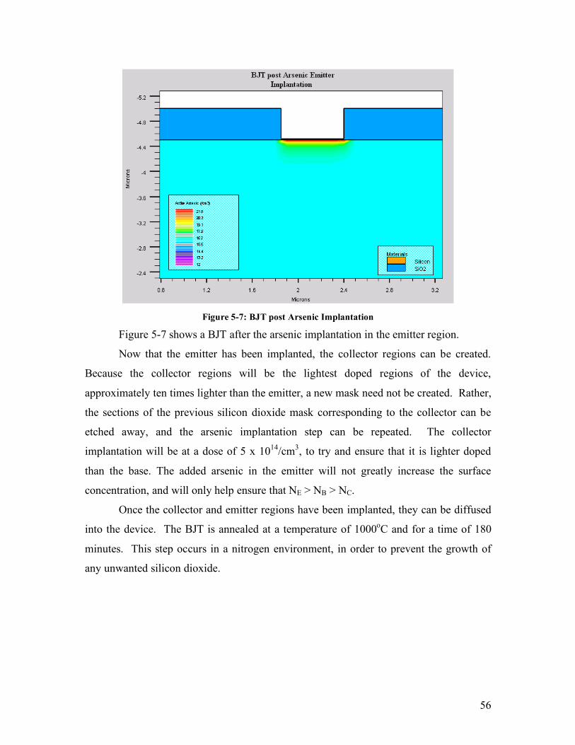
56
Figure 5-7: BJT post Arsenic Implantation
Figure 5-7 shows a BJT after the arsenic implantation in the emitter region.
Now that the emitter has been implanted, the collector regions can be created.
Because the collector regions will be the lightest doped regions of the device,
approximately ten times lighter than the emitter, a new mask need not be created. Rather,
the sections of the previous silicon dioxide mask corresponding to the collector can be
etched away, and the arsenic implantation step can be repeated. The collector
implantation will be at a dose of 5 x 10¹⁴/cm3, to try and ensure that it is lighter doped
than the base. The added arsenic in the emitter will not greatly increase the surface
concentration, and will only help ensure that NE > NB > NC.
Once the collector and emitter regions have been implanted, they can be diffused
into the device. The BJT is annealed at a temperature of 1000oC and for a time of 180
minutes. This step occurs in a nitrogen environment, in order to prevent the growth of
any unwanted silicon dioxide.
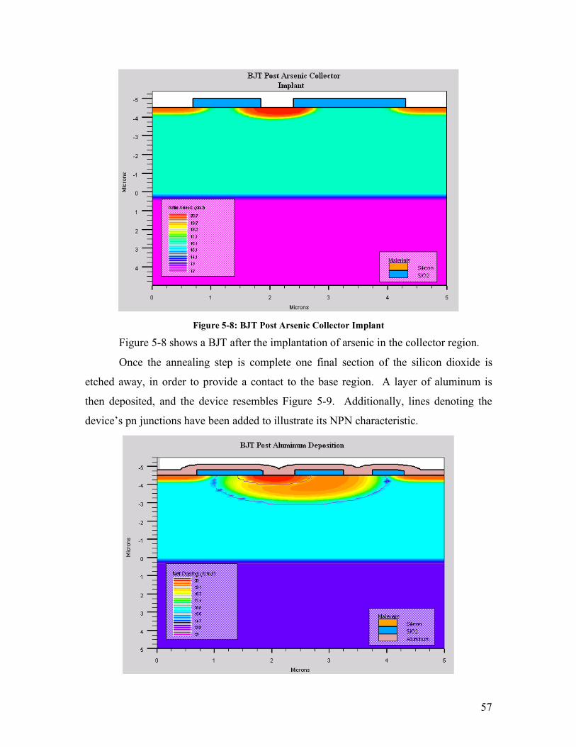
57
Figure 5-8: BJT Post Arsenic Collector Implant
Figure 5-8 shows a BJT after the implantation of arsenic in the collector region.
Once the annealing step is complete one final section of the silicon dioxide is
etched away, in order to provide a contact to the base region. A layer of aluminum is
then deposited, and the device resembles Figure 5-9. Additionally, lines denoting the
device’s pn junctions have been added to illustrate its NPN characteristic.
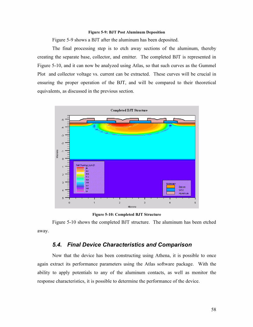
58
Figure 5-9: BJT Post Aluminum Deposition
Figure 5-9 shows a BJT after the aluminum has been deposited.
The final processing step is to etch away sections of the aluminum, thereby
creating the separate base, collector, and emitter. The completed BJT is represented in
Figure 5-10, and it can now be analyzed using Atlas, so that such curves as the Gummel
Plot and collector voltage vs. current can be extracted. These curves will be crucial in
ensuring the proper operation of the BJT, and will be compared to their theoretical
equivalents, as discussed in the previous section.
Figure 5-10: Completed BJT Structure
Figure 5-10 shows the completed BJT structure. The aluminum has been etched
away.
5.4. Final Device Characteristics and Comparison
Now that the device has been constructing using Athena, it is possible to once
again extract its performance parameters using the Atlas software package. With the
ability to apply potentials to any of the aluminum contacts, as well as monitor the
response characteristics, it is possible to determine the performance of the device.
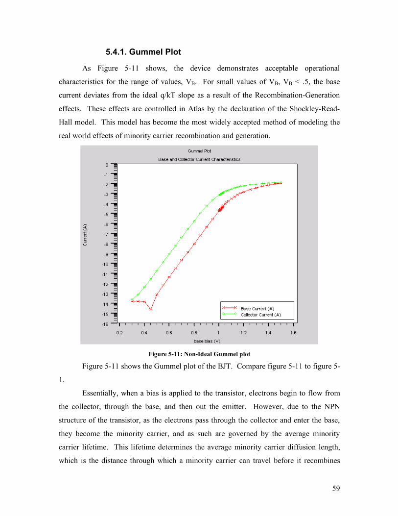
59
5.4.1. Gummel Plot
As Figure 5-11 shows, the device demonstrates acceptable operational
characteristics for the range of values, VB. For small values of VB, VB < .5, the base
current deviates from the ideal q/kT slope as a result of the Recombination-Generation
effects. These effects are controlled in Atlas by the declaration of the Shockley-Read-
Hall model. This model has become the most widely accepted method of modeling the
real world effects of minority carrier recombination and generation.
Figure 5-11: Non-Ideal Gummel plot
Figure 5-11 shows the Gummel plot of the BJT. Compare figure 5-11 to figure 5-
1.
Essentially, when a bias is applied to the transistor, electrons begin to flow from
the collector, through the base, and then out the emitter. However, due to the NPN
structure of the transistor, as the electrons pass through the collector and enter the base,
they become the minority carrier, and as such are governed by the average minority
carrier lifetime. This lifetime determines the average minority carrier diffusion length,
which is the distance through which a minority carrier can travel before it recombines
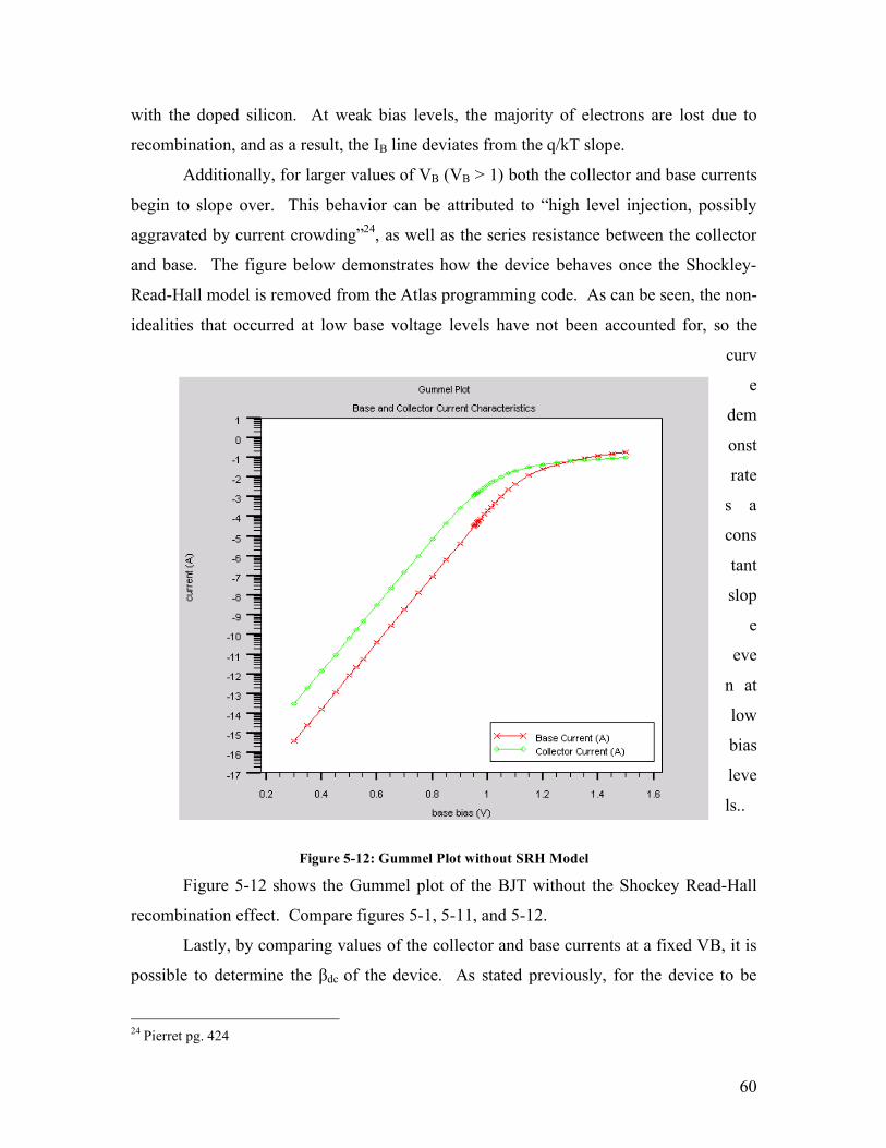
60
with the doped silicon. At weak bias levels, the majority of electrons are lost due to
recombination, and as a result, the IB line deviates from the q/kT slope.
Additionally, for larger values of VB (VB > 1) both the collector and base currents
begin to slope over. This behavior can be attributed to “high level injection, possibly
aggravated by current crowding”24, as well as the series resistance between the collector
and base. The figure below demonstrates how the device behaves once the Shockley-
Read-Hall model is removed from the Atlas programming code. As can be seen, the non-
idealities that occurred at low base voltage levels have not been accounted for, so the
curv
e
dem
onst
rate
s a
cons
tant
slop
e
eve
n at
low
bias
leve
ls..
Figure 5-12: Gummel Plot without SRH Model
Figure 5-12 shows the Gummel plot of the BJT without the Shockey Read-Hall
recombination effect. Compare figures 5-1, 5-11, and 5-12.
Lastly, by comparing values of the collector and base currents at a fixed VB, it is
possible to determine the βdc of the device. As stated previously, for the device to be
24 Pierret pg. 424
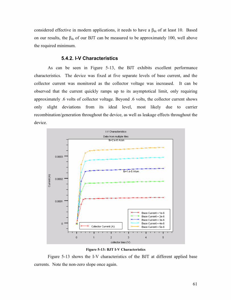
61
considered effective in modern applications, it needs to have a βdc of at least 10. Based
on our results, the βdc of our BJT can be measured to be approximately 100, well above
the required minimum.
5.4.2. I-V Characteristics
As can be seen in Figure 5-13, the BJT exhibits excellent performance
characteristics. The device was fixed at five separate levels of base current, and the
collector current was monitored as the collector voltage was increased. It can be
observed that the current quickly ramps up to its asymptotical limit, only requiring
approximately .6 volts of collector voltage. Beyond .6 volts, the collector current shows
only slight deviations from its ideal level, most likely due to carrier
recombination/generation throughout the device, as well as leakage effects throughout the
device.
Figure 5-13: BJT I-V Characteristics
Figure 5-13 shows the I-V characteristics of the BJT at different applied base
currents. Note the non-zero slope once again.
62
5.5. Conclusion
Similar to the construction of the NMOS transistor, the creation of the BJT gave
us valuable insight into the design challenges of fabricating a BJT. Most importantly was
the modulation of the base width, which proved to have the biggest effect on the
performance of the device. While having a thick base is ideal for large reverse
breakdown voltages, it also increases the threshold voltage of the device. Additionally,
the minority carrier lifetime must be taken into consideration, as demonstrated in Figures
1-11 and 1-12. Once the time for a minority carrier to travel through the base exceeds the
average lifetime, the device will exhibit poor operating characteristics at low voltages,
and much of the current will be lost.
6. LDMOS Transistor The final device left to create in the project was the LDMOS transistor. We had
already had the practice of creating the CMOS transistor, from sample Silvaco structures,
and creating the lateral BJT, modeling it after a different form of BJT. Next, we had to
create the most difficult device of all three, the LDMOS. The LDMOS was an unfamiliar
device to us. Furthermore, there were no Silvaco examples to facilitate the coding
process. Therefore, we had to code the entire device from beginning to end, using our
knowledge from previous experience.
6.1. Problem Statement
Create a functional LDMOS that performs to BCD-III standards. With no
samples of an LDMOS simulation at hand, we took our time and came up with a logical
design process recipe to ensure the efficiency of masking steps.
The LDMOS’ dimensions would be 20 µm wide and 12.5µm tall. This device
was the largest device simulated yet. Moreover, it was unlike either of the previous
structures in that it is a-symmetrical. In combination, the large size, and the inability to
“mirror” the device, created large computational times. Thus, it was difficult to simulate.
The dimensions of the structure were chosen because of the characteristics of the
device. A deep channel, and an additional oxide layer are both necessary to obtain
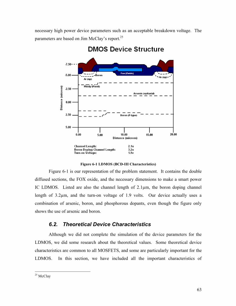
63
necessary high power device parameters such as an acceptable breakdown voltage. The
parameters are based on Jim McClay’s report.25
Figure 6-1 LDMOS (BCD-III Characteristics)
Figure 6-1 is our representation of the problem statement. It contains the double
diffused sections, the FOX oxide, and the necessary dimensions to make a smart power
IC LDMOS. Listed are also the channel length of 2.1µm, the boron doping channel
length of 3.2µm, and the turn-on voltage of 1.9 volts. Our device actually uses a
combination of arsenic, boron, and phosphorous dopants, even though the figure only
shows the use of arsenic and boron.
6.2. Theoretical Device Characteristics
Although we did not complete the simulation of the device parameters for the
LDMOS, we did some research about the theoretical values. Some theoretical device
characteristics are common to all MOSFETS, and some are particularly important for the
LDMOS. In this section, we have included all the important characteristics of
25 McClay
64
MOSFETs, and theoretical analysis for the relevant ones. All of the issues are discussed
even if they are not very important to the LDMOS. Some of these issues came during the
simulation process. For example, if leakage current is not expected to be a problem in the
device, but it is during simulation, then it may be encouraging to understand how leakage
current works. All though we have not applied all of the theoretical values, we have
given many theoretical equations and other applied research.
6.2.1. Threshold Voltage
!!"
#$$%
&'=
i
Df
n
N
q
kTln( Equation 4
)(4
20
F
S
D
O
oS
FTK
qN
K
xKV !
"! ##= Equation 5
Using the same threshold voltage equations apply to the LDMOS. The threshold
is based on temperature, the doping of the device, some constants, and the device
parameters. This measurement is taken by shorting the drain and the gate, and finding a
value for which a specific drain current occurs at the threshold voltage level.26 This is a
common characteristic of any MOSFET device. Plugging in our numbers for the doping
profile and the device parameters, we obtain a turn-on voltage of 1.8V.
6.2.2. Leakage Current
This is a common characteristic of any MOSFET. This characteristic is
particularly unimportant for the LDMOS device. Leakage current is generally not an
issue with most DMOS circuits. Common gate to body leakage currents are around a
picoampere.27
This characteristic is dependant upon the doping profile of the wafer, epitaxial
layer and the drain. It is also dependant upon the depth of the device. In the case of the
LDMOS, it is desired to have the epitaxial layer far enough away from the drain to not
alter the junction lines of the device. The LDMOS device for BCD-III standards is fairly
26 Supertex pg. 3.1 27 Supertex pg. 3.1
65
deep. This increases the resistance along the path and does not allow for a large leakage
current.28
Leakage current is dependent upon temperature. As heat builds on the LDMOS,
leakage current also increases.29
Leakage current is governed by the following equations:
Ilk = (qAjni/2τ0)(xd) Equation 6 Leakage Current
Where, Aj = junction area
Ni = intrinsic carrier concentration
τ0 = intrinsic carrier concentration
xd = thickness of depletion region30
τ0 = (τn + τp)/2 Equation 7 Intrinsic Carrier Concentration
Where, τ0 = intrinsic carrier concentration
Τn = donor carrier concentration
Τp = acceptor carrier concentration31
6.2.3. Off-State Leakage Current
The off-state leakage current occurs in transistors when there are zero volts from
gate to source, but a voltage from drain to source is applied. The current escapes from
the body of the transistor that forms a reverse bias diode. Losses are common to
diffusion. Once again, this characteristic is not crucial to the LDMOS.32
The off-state leakage current is also greatly affected by the depth of the device.
Once again, the 5µm deep device should offer enough protection against off-state leakage
current.33
Off-state leakage current is governed by the same equations as on-state leakage
current.
28 Supertex pg. 3.1 29 Analog Integrated Circuit Design pg. 42 30 Ibid pg. 42 31 Ibid pg. 42 32 Supertex pg. 3.1 33 Ibid pg. 3.1
66
6.2.4. Breakdown Voltage
This characteristic is particularly important for the LDMOS device. A high
breakdown voltage is the main characteristic that separates it from other MOS devices. It
is the reason why BCD technology has been called “smart power”.
Breakdown voltage is measured by applying a current through the drain and the
source, and measuring the voltage across the channel (the channel has some on-
resistance). This parameter is likely to degrade over multiple uses of the device because
of thermal reasons.34
The double diffusion plays a major role in the breakdown voltage characteristic of
an LDMOS transistor. Together, the two oppositely doped regions within the deep p-
well drive act as diodes opposing each other. The dopings are variable, and they offer
high voltage blocking characteristics.
Also, the breakdown voltage is highly dependent upon the depth of the channel
within the device. The longer channel drift length, the larger the breakdown voltage can
be.35
The breakdown voltage is also dependent upon the doping conentration and
positioning of the epitaxial layer (or the substrate if there is no epitaxial layer). A much
higher voltage is able to be applied in the case of lower doped/ thinner epitaxial layer.
The reason for this is because the field at the surface is below critical field due to the
change in charge distribution.36
The breakdown voltage is dependent upon the shape/ position of the contacts.
They affect the curvature of the electric field lines. The affects due to the contacts are
more prominent in smaller devices.37 More importantly, the curvature of the junction
depicts a change in the breakdown voltage (which is affected by the contacts).38 Small
Signal Transconductance
gm = (VGS – VGS(TH))(µoff Zعox)/(Ltox) Equation 8 Small Signal Transconductance
34 Supertex pg. 3.1-2 35 Chang Mf pg. 1996 36 Appels pg. 238 37 Ibid pg. 238 38 Chang Mf pg. 1992
67
Where, Z/L = source perimeter/Channel length
µoff = Effective carrier mobility
ox = Gate Dielectric constantع
tox = Gate Oxide Thickness
Small signal transconductance is considered to be the ratio of the change in
current through the drain and the change in gate to source voltage.39
This can be a crucial characteristic in determining the current gain of an LDMOS.
More equations that govern small signal transconductance are as follows:
gm = 2ID/Veff Equation 9 Small Signal Transconductance (ID and Veff)
gm = (2µnCox(W/L)ID)1/2 Equation 10 Small Signal Transconductance (Cox and ID)
gm = µnCox (W/L) Veff Equation 11 Small Signal Transconductance (Cox and Veff)40
6.2.5. On-Resistance
This characteristic is particularly important for the LDMOS device. It is
dependent upon temperature (as the temperature of a MOSFET increases, carrier mobility
decreases, thereby reducing “…current for a given voltage”)41, diffusion length, and the
material. It is measured by dividing a given drain to source voltage by a given drain
current. Typical on-resistances for LDMOS structures range between 0.5Ω – 2Ω for high
power devices and 2Ω-5Ω for low voltage applications.42
39 Supertex pg. 3.1-2 40 Analog Integrated Circuit Design pg. 29-30 41 Supertex pg. 3.3 42 Ibid pg 3.3
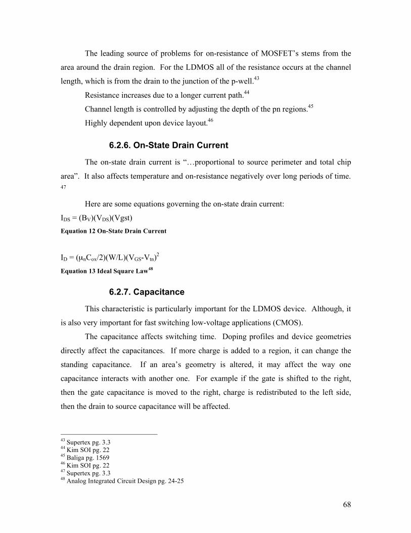
68
The leading source of problems for on-resistance of MOSFET’s stems from the
area around the drain region. For the LDMOS all of the resistance occurs at the channel
length, which is from the drain to the junction of the p-well.43
Resistance increases due to a longer current path.44
Channel length is controlled by adjusting the depth of the pn regions.45
Highly dependent upon device layout.46
6.2.6. On-State Drain Current
The on-state drain current is “…proportional to source perimeter and total chip
area”. It also affects temperature and on-resistance negatively over long periods of time. 47
Here are some equations governing the on-state drain current:
IDS = (BV)(VDS)(Vgst) Equation 12 On-State Drain Current
ID = (µnCox/2)(W/L)(VGS-Vtn)2 Equation 13 Ideal Square Law48
6.2.7. Capacitance
This characteristic is particularly important for the LDMOS device. Although, it
is also very important for fast switching low-voltage applications (CMOS).
The capacitance affects switching time. Doping profiles and device geometries
directly affect the capacitances. If more charge is added to a region, it can change the
standing capacitance. If an area’s geometry is altered, it may affect the way one
capacitance interacts with another one. For example if the gate is shifted to the right,
then the gate capacitance is moved to the right, charge is redistributed to the left side,
then the drain to source capacitance will be affected.
43 Supertex pg. 3.3 44 Kim SOI pg. 22 45 Baliga pg. 1569 46 Kim SOI pg. 22 47 Supertex pg. 3.3 48 Analog Integrated Circuit Design pg. 24-25

69
These are the three main capacitances in MOSFET’s. They can be calculated by
finding other values of capacitances.49
CISS = CGS + CDG Equation 14Input Capacitance
CRSS = CDG Equation 15 Common source capacitance
COSS = CDS + CDG Equation 16 Reverse transfer capacitance
Here are the remaining equations to obtain the values for the above equations:
Cox = Kox єo /tox Equation 17 Oxide Capacitance
Cgs(approximately)= 2/3WLCox Equation 18 Gate Capacitance
CDG = CoxWLov Equation 19 Drain to Gate Capacitance
CGD = WLCox/2 Equation 20 Gate to Drain Capacitance50
6.3. Walkthrough of LDMOS Fabrication
Provided is a walkthrough of the simulation of the fabrication process for the
LDMOS.
49 Supertex pg. 3.3 50 Analog Integrated Circuit Design pg. 21
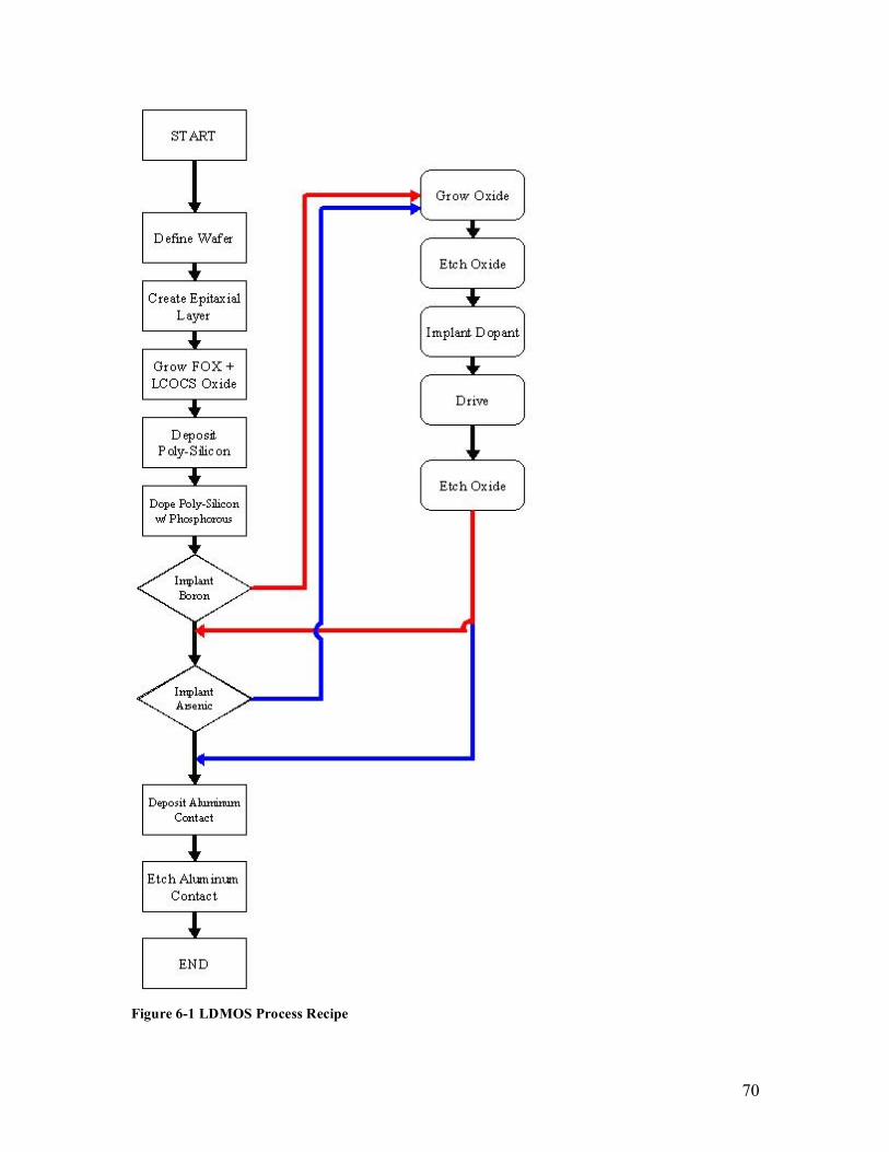
70
Figure 6-1 LDMOS Process Recipe
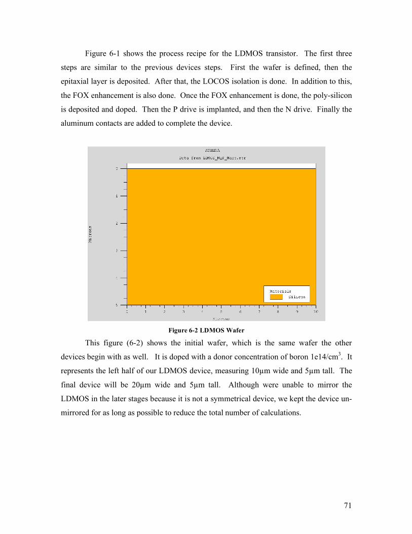
71
Figure 6-1 shows the process recipe for the LDMOS transistor. The first three
steps are similar to the previous devices steps. First the wafer is defined, then the
epitaxial layer is deposited. After that, the LOCOS isolation is done. In addition to this,
the FOX enhancement is also done. Once the FOX enhancement is done, the poly-silicon
is deposited and doped. Then the P drive is implanted, and then the N drive. Finally the
aluminum contacts are added to complete the device.
Figure 6-2 LDMOS Wafer
This figure (6-2) shows the initial wafer, which is the same wafer the other
devices begin with as well. It is doped with a donor concentration of boron 1e14/cm3. It
represents the left half of our LDMOS device, measuring 10µm wide and 5µm tall. The
final device will be 20µm wide and 5µm tall. Although were unable to mirror the
LDMOS in the later stages because it is not a symmetrical device, we kept the device un-
mirrored for as long as possible to reduce the total number of calculations.
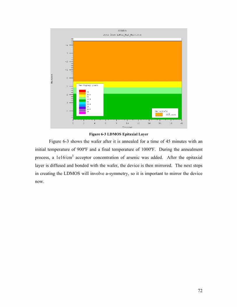
72
Figure 6-3 LDMOS Epitaxial Layer
Figure 6-3 shows the wafer after it is annealed for a time of 45 minutes with an
initial temperature of 900ºF and a final temperature of 1000ºF. During the annealment
process, a 1e16/cm3 acceptor concentration of arsenic was added. After the epitaxial
layer is diffused and bonded with the wafer, the device is then mirrored. The next steps
in creating the LDMOS will involve a-symmetry, so it is important to mirror the device
now.
73
Figure 6-4 FOX Enhancement and LOCOS Isolation
Figure 6-4 shows the completion of the next masking step. We want to apply the
nitride mask in the proper places to put the oxide layer exactly where we want it to be.
The oxide will be used for both the LOCOS isolation (see section 3.3.4) and the FOX
enhancement. Both of these types of oxidation need to occur early in the design process
to allow time for them to grow in other annealing steps. The oxides are grown and
diffused for a time of 60 minutes and for a temperature of 1100ºF using a wet oxidation
process.
FOX enhancement is a layer of oxidation beneath the poly-silicon and gate oxide
that serves to boost performance parameters. It creates a deeper channel for current to
travel, while still minimizing the length of the channel. The depth of the channel greatly
affects the break down voltage of the device. For a power IC device, a high breakdown
voltage is desired. A short channel length greatly reduces the on-resistance of the device.
A minimal on-resistance is desired, it will allow for much higher current applications.
FOX enhancement provides a solution to the breakdown voltage and on-resistance trade-
off issue.51
51 McClay
74
Figure 6-5 LDMOS with Poly-silicon
Figure 6-5 shows the poly-silicon layer after it has been deposited on the surface
of the device. Prior to the deposition layer of poly-silicon, the wafer was diffused for 10
minutes at a temperature of 1035ºF in a dry atmosphere. This allowed for the bonding of
the existing layer, and for the separation of it from the new poly-silicon layer.
During this step, the doping profile has also changed. Although it is not visible
with this figure, one can see the doping profile in the next figure (6-6). During this
process step, ion implantation of a donor concentration of 3e13/cm3 was added using an
energy of 20 pearsons. The poly-silicon takes on a new doping profile of 3e13 cm3.
75
Figure 6-6 LDMOS Active Boron Dose
The next masking step involved the implantation of the boron n-type donor
concentration into the device. Here the poly-silicon was unaffected by the implantation
regardless of the color of the poly-silicon. Since ion implantation is used, essentially
hitting anything on the surface with the boron dose is avoidable. The poly-silicon was
etched away on the left side to allow a higher concentration of boron at the surface on
that side. The boron was implanted at a concentration of 5e15/cm3 at an energy of 100
pearsons. The wafer was diffused for a time of 150 minutes at a temperature of 1100ºF in
a nitrogen atmosphere. (As shown in figure 6-6).
76
Figure 6-7 LDMOS 2nd Oxide Layer
The next figure (figure 6-7) shows the LDMOS device prior to the masking of the
p-well drive (see figure 6-8). To prepare for the next ion implantation step the poly-
silicon was etched away on the right side. In addition, a small surface of oxide (0.05µm)
was also etched. This ensures that, when the new gate oxide layer is grown, it surrounds
the channel in the proper areas isolating junctions and leakage currents. After it was
etched, the new gate oxide was then grown at a thickness of 0.5µm. This oxide layer also
serves as a mask for the upcoming p-well drive process step.
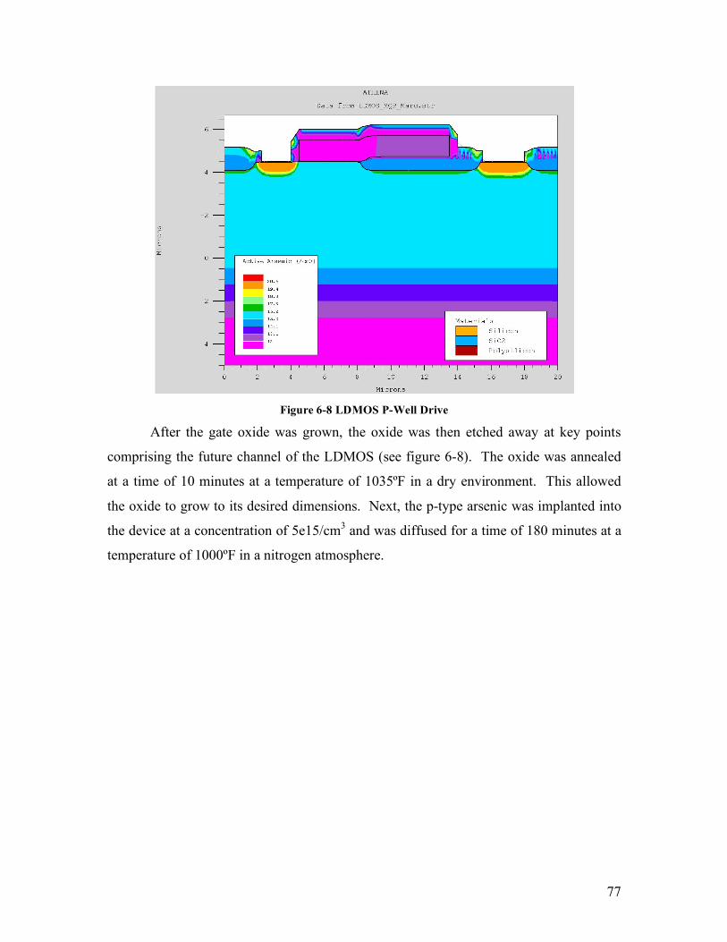
77
Figure 6-8 LDMOS P-Well Drive
After the gate oxide was grown, the oxide was then etched away at key points
comprising the future channel of the LDMOS (see figure 6-8). The oxide was annealed
at a time of 10 minutes at a temperature of 1035ºF in a dry environment. This allowed
the oxide to grow to its desired dimensions. Next, the p-type arsenic was implanted into
the device at a concentration of 5e15/cm3 and was diffused for a time of 180 minutes at a
temperature of 1000ºF in a nitrogen atmosphere.
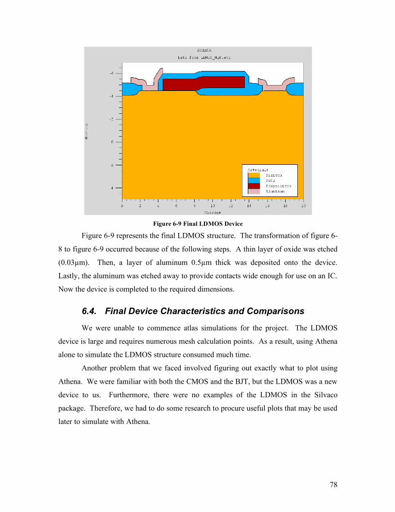
78
Figure 6-9 Final LDMOS Device
Figure 6-9 represents the final LDMOS structure. The transformation of figure 6-
8 to figure 6-9 occurred because of the following steps. A thin layer of oxide was etched
(0.03µm). Then, a layer of aluminum 0.5µm thick was deposited onto the device.
Lastly, the aluminum was etched away to provide contacts wide enough for use on an IC.
Now the device is completed to the required dimensions.
6.4. Final Device Characteristics and Comparisons
We were unable to commence atlas simulations for the project. The LDMOS
device is large and requires numerous mesh calculation points. As a result, using Athena
alone to simulate the LDMOS structure consumed much time.
Another problem that we faced involved figuring out exactly what to plot using
Athena. We were familiar with both the CMOS and the BJT, but the LDMOS was a new
device to us. Furthermore, there were no examples of the LDMOS in the Silvaco
package. Therefore, we had to do some research to procure useful plots that may be used
later to simulate with Athena.
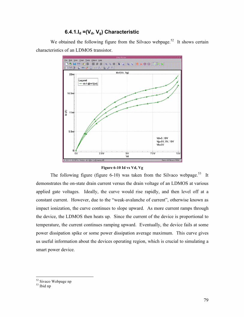
79
6.4.1.Id =(Vd, Vg) Characteristic
We obtained the following figure from the Silvaco webpage.52 It shows certain
characteristics of an LDMOS transistor.
Figure 6-10 Id vs Vd, Vg
The following figure (figure 6-10) was taken from the Silvaco webpage.53 It
demonstrates the on-state drain current versus the drain voltage of an LDMOS at various
applied gate voltages. Ideally, the curve would rise rapidly, and then level off at a
constant current. However, due to the “weak-avalanche of current”, otherwise known as
impact ionization, the curve continues to slope upward. As more current ramps through
the device, the LDMOS then heats up. Since the current of the device is proportional to
temperature, the current continues ramping upward. Eventually, the device fails at some
power dissipation spike or some power dissipation average maximum. This curve gives
us useful information about the devices operating region, which is crucial to simulating a
smart power device.
52 Sivaco Webpage np 53 Ibid np
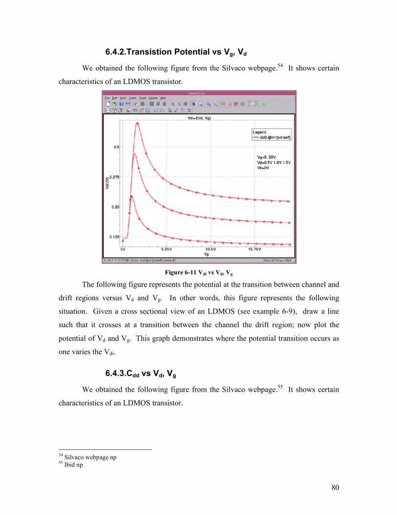
80
6.4.2.Transistion Potential vs Vg, Vd
We obtained the following figure from the Silvaco webpage.54 It shows certain
characteristics of an LDMOS transistor.
Figure 6-11 Vdi vs Vd, Vg
The following figure represents the potential at the transition between channel and
drift regions versus Vd and Vg. In other words, this figure represents the following
situation. Given a cross sectional view of an LDMOS (see example 6-9), draw a line
such that it crosses at a transition between the channel the drift region; now plot the
potential of Vd and Vg. This graph demonstrates where the potential transition occurs as
one varies the Vdi.
6.4.3.Cdd vs Vd, Vg
We obtained the following figure from the Silvaco webpage.55 It shows certain
characteristics of an LDMOS transistor.
54 Silvaco webpage np 55 Ibid np
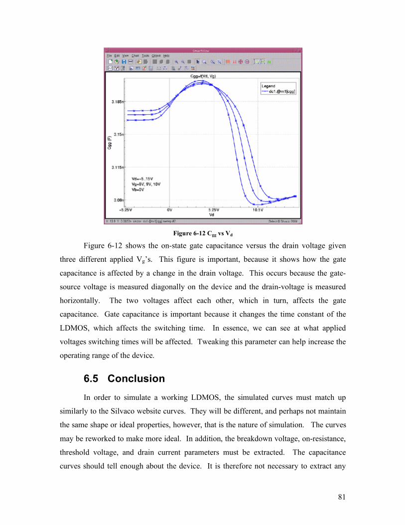
81
Figure 6-12 Cgg vs Vd
Figure 6-12 shows the on-state gate capacitance versus the drain voltage given
three different applied Vg’s. This figure is important, because it shows how the gate
capacitance is affected by a change in the drain voltage. This occurs because the gate-
source voltage is measured diagonally on the device and the drain-voltage is measured
horizontally. The two voltages affect each other, which in turn, affects the gate
capacitance. Gate capacitance is important because it changes the time constant of the
LDMOS, which affects the switching time. In essence, we can see at what applied
voltages switching times will be affected. Tweaking this parameter can help increase the
operating range of the device.
6.5 Conclusion In order to simulate a working LDMOS, the simulated curves must match up
similarly to the Silvaco website curves. They will be different, and perhaps not maintain
the same shape or ideal properties, however, that is the nature of simulation. The curves
may be reworked to make more ideal. In addition, the breakdown voltage, on-resistance,
threshold voltage, and drain current parameters must be extracted. The capacitance
curves should tell enough about the device. It is therefore not necessary to extract any

82
capacitances other than the value gate capacitance. These are the parameters and curves
that best describe the LDMOS transistor.

83
7. BCD Fabrication Wafer A single device is easy enough to simulate and achieve stellar results for a relativlely
inexpensive amount of money. The problem arises when multiple devices are produced
on a single wafer. This section discusses in detail the problems that arise when creating a
wafer with multiple devices. In addition, shrinking device parameters will also be
discussed.
7.1. Problem Statement The initial problem statement was to simulate combining the CMOS, BJT, and
LDMOS devices onto a single wafer while conforming to BCD-III standards. Due to
time constraints we could not simulate the optimization of the three devices onto a single
wafer.
The new problem statement was to research strategies for optimization and analyze
the fabrication of the three devices on a single wafer. Also, part of the new problem
statement was to analyze problems that might arise when taking a BCD-III wafer and
shrinking it down to BCD-V standards.
7.2. Process Recipe In order to solve the problem, a process recipe had to be created in order to analyze
the effect of changing a single process step on the fabrication process as a whole. A
walkthrough of the recipe is given in this section.
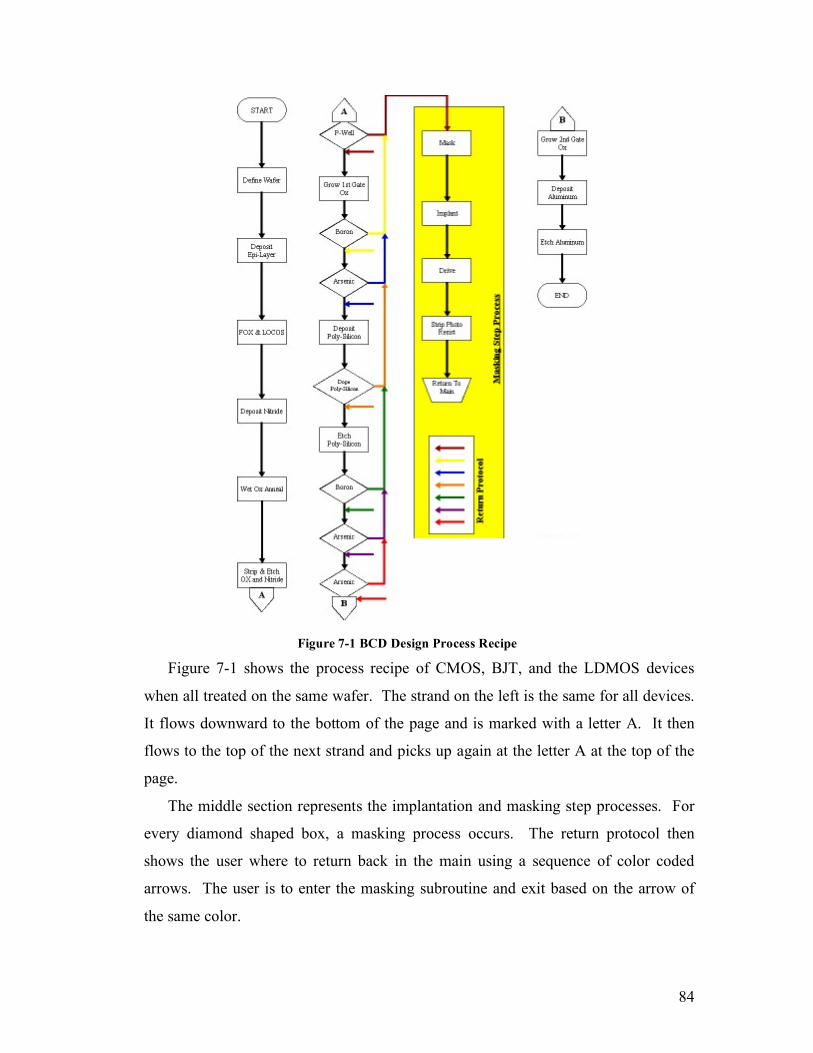
84
Figure 7-1 BCD Design Process Recipe
Figure 7-1 shows the process recipe of CMOS, BJT, and the LDMOS devices
when all treated on the same wafer. The strand on the left is the same for all devices.
It flows downward to the bottom of the page and is marked with a letter A. It then
flows to the top of the next strand and picks up again at the letter A at the top of the
page.
The middle section represents the implantation and masking step processes. For
every diamond shaped box, a masking process occurs. The return protocol then
shows the user where to return back in the main using a sequence of color coded
arrows. The user is to enter the masking subroutine and exit based on the arrow of
the same color.
85
The section on the right represents the final touches that all the devices go through
during fabrication. Follow the implantation string to the bottom of the page where
the letter B flows to. That letter B connects to the letter B in the process string on the
top of the page all the way to the right.
7.3. Strategies for maximizing Performance Parameters LDMOS accounts for 30%-70% of total BCD die surface area. Therefore it is
important to maximize the performance of the LDMOS parameters, more so than the
other devices. There are additional tradeoffs that occur with other devices as well.
7.3.1. Capacitance
The LDMOS has a high switching speed and high input impedance.56 So
compromising this factor may be to the advantage of the user. Characteristically, doping
the substrate more highly can increase the gate capacitance. This will lower the
switching time. However, this also increases the amount of charge at the junction,
thereby allowing the breakdown voltage to increase
Problems with this are quite apparent. If the substrate or epitaxial layer are more
highly doped, then the BJT may not have the same amplifying properties that it should
have. Furthermore, if the capacitances of the CMOS transistors are increased, then their
switching speeds too are greatly reduced. For the purposes of BCD technology, this is
not acceptable.
If the substrate is too lightly doped (for optimized CMOS) then the LDMOS can
suffer from punch through. That occurs when the pinched off current sneaks around the
desired channel. It is not desirable.
7.3.2. Surface Field Reduction
High electric field at the surface is undesirably. It lowers the breakdown voltage and
influences the on-resistance, the two most valuable parameters that affect the LDMOS.
Limitations are being reached by using FOX enhancement (one way of reducing the
surface field).
56 Rossel Advanced pg. 119
86
One way to alter this is to change the junction of the double diffused region. If this
parameter can be optimized (shank to its minimal functional size), then the LDMOS will
have great characteristics. A problem with this is that the CMOS source and drain
regions may not extend far enough down. This will cause the pinch-off factor to be
increase greatly along with short channel effects.
7.3.3. Process Problems Even if the devices are simulated exactly how you want them individually, the
process parameters that occur later in the recipe can affect them. For example, if the
CMOS is correctly diffused the right amount downward into the wafer, later it may
expand too far due to later annealment steps. This can present many problems.
7.4. Strategies For Improving Shrinking Device Geometry There are multiple strategies for improving the BCD devices. Much of the
strategies are geared toward the LDMOS. Furthermore, certain methods are
starting to reach their limits, and new technology needs to be developed in order
to overcome shrinking issues.
7.4.1 VLSI technology shrinking Poly-Silicon Window Using VLSI for improving many of the LDMOS’s parameters is out of the
question. It is too difficult. However, using VLSI technology can be used to
shrink the poly-silicon window. The result is improved current distribution within
the cell.57 Using this method, on-resistance can be reduced by a factor of 2X.58
However, that is approaching the theoretical limit 0.15 ohms. Therefore other
forms of technology are also necessary.
7.4.2. Trench gate structure One form of trench gate synthesis is using the LUDMOS. It is a trench in the drift
region under the gate to reduce electric field at the surface. Now, breakdown
voltage is governed by trench depth instead of charge at the surface. Now the
drain can be placed close to the trench. The trench can be partially filled with
poly-silicon, which helps with conduction. Now the epitaxial layer can be doped 57 Baliga 1569 58 Baliga pg. 1569
87
more highly without worrying about punch-through. The result is an increase in
active area and a much lower on-resistance.59
7.4.3. Materials One Example of a different material other than silicon is the use of Gallium
arsenide. Currently it is very costly. However, as production increases, the price of
GaAs is dramatically decreasing, and it may soon become available more readily. It is
beneficial to BCD technology because it is 3-5 times smaller module size. Also, it has
better diffusion properties when doped.
Another example is Silicon carbide. It can reduce on resistance by over 100
times.60
7.4.4. Tapered Oxide (TEOS) Another way to reduce the field oxide and optimize BCS technology is by tapering
the field oxide. It is more difficult to grow this type of oxide, which may be a cost design
issue. With it, Boron in the drift region in particular performs better, and current
distribution is very good.61Furthermore the “boron out diffusion and reduced current
path” are improved.62
7.5. Conclusion There are many ways of improving BCD technology currently. There are ways to
optimize the devices and there are new forms of technology being introduced to aid the
BCD characteristics. BCD technology needs to be implemented and simulated on even
smaller level. Better BCD technology is in our grasp.
59 Rossel Advanced pg. 119 60 Baliga pg. 1569 61 Kim SOI pg. 25 62 Ibid pg. 21
88
8. Project Summary and Future Work When we began our MQP, it was decided that this project would be, more than
anything, a chance to learn. Rather than focus on endlessly tweaking the Athena code in
pursuit of incremental performance gains of the BCD components, we felt it was
significantly more important to pursue the knowledge, skills, and abilities that the field of
semiconductor device design requires. This project was an opportunity to learn about
both the BCD fabrication process, as well as the Silvaco suite of modeling applications,
which are used throughout the semiconductor industry to model the behavior of BCD
devices. Now that the project is complete, we recognize that we have learned an
extensive amount about both the fabrication process, as well as the real world issues
confronting component designers. In this respect, we feel that our project has been a
success.
We started this project with little more than an Atlas example showing the
fabrication of a 1.2 micron NPN transistor. Since then, we have become much more
proficient with Silvaco. We have improved our abilities to the point where we no longer
require an example of a device in order to create a functional BCD component. Through
the use of Athena and Atlas, we are now able to design and test all manner of devices.
Using formulas and equations from our research to supplement our calculations we were
able to create working BCD devices with parameters close to those of the BCD-III family
of ICs.
Our research has also come a long way, as we both know significantly more about
the fabrication process than we did at the beginning of the project. We’ve learned the
fundamentals, such as applying a photo resist in order to protect areas of the wafer during
the etching process, using ion implantation to deposit ions below the surface of silicon,
and how ion implantation results in a near Gaussian distribution of the ions within the
silicon. We have also devoted research efforts to learning about more advanced
techniques, like trench isolation, LOCOS, and RESURF.
While it is true that we have come a long way over the course of this project, we
recognize that there is still more that can be done. The BCD devices that we have created
demonstrate acceptable, however not production-worthy, performance characteristics. As

89
our focus was on acquiring the skills and knowledge to create the devices, we did not feel
it was as important to strive for a commercially viable fabrication process. Additionally,
information regarding the LDMOS has been sparse, so we recognize that further efforts
can be devoted to the design and testing of this component. We were able to achieve an
LDMOS model, however it remains as of yet, untested.
90
Appendix A – References 1)Appels JA and Vaes HMJ (1979) High-Voltage Thin-Layer Devices (RESURF
Devices), IEDM Tech Dig, pp 238-241
2)Baliga, B. Jayant, IEEE Transactions on Electron Devices, Vol. 38. No. 7: An
Overview of Smart Power Technology, July 1991.
3)Chang MF, Piefer G, Yilmaz H, Wildi EJ, Hodgins RG, Owyang K and Adler MS
(1986) IEEE Trans Electron Devices vol ED-33, pp 1992-2001
4)Jaeger, Richard C., Modular Series On Solid State Devices Volume V:Introduction
to Microelectronic Fabrication. Addison-Wesley Publishing Company, 1988
5)Johns, David A., Martin, Ken, Analog Integrated Circuit Design, John Wiley and Sons
Inc., New York, 1997
6)Kim, Jongdae, ETRI Journal Volume 21, Number 3: Characteristics of P-channel SOI
LDMOS Transistor with Tapered Field Oxides, September 1999
7)Mauro, Zambuto, Semiconductor Devices, McGraw Hill Book Company, New York,
1989
8)McClay, James M. Personnel Communication.
9)Moreau, Wayne M., Semiconductor Lithography: Principles , Practices, and Materials.
Plenum Press: New York, 1988.
10)Murari, B. Bertotti, F. Vignola, G.A. (Eds.), Smart Power IC’s: Technologies and
Applications, Springer: Berlin, 2002.
91
11)Pierret, Robert F., Semiconductor Device Fundamentals, Addison-Wesley Publishing
Company, 1996
12)RF Micro Devices, Augustine, Paul J., Trends and Opportunities for Gallium
Arsenide Semiconductors in Handsets, 2005
13)Rossel, P., Proc 22nd International Conference on Microelectronics Vol. 1: Advanced
Concepts in Smart Power Integrated Circuits, May 2000
14)Roulston, David J., Bipolar Semiconductor Devices, McGraw Hill Book Company,
Newy York, 1990
15)Supertex Inc., Databook 1993-1994: High Voltage Integrated Circuits and DMOS
Transistors, Supertex, 1993
16)Sze, S.M., Semiconductor Devices: Physics and Technology, AT&T Bell Labratories:
New York, 1985.
17)Warner Jr., R. M., Grung, B. L., Semiconductor-Device Electronics, Saunders College
Publishing, 1991
18)[email protected]., Silvaco Inc: Webpage,
https://src.silvaco.com/ResourceCenter/en/SimulationStandard/showArticle.jsp?y
ear=2004&article=a2&month=jan, 2006
19)Yang, Edward S., Fundamentals of Semiconductor Devices, McGraw Hill Book
Company, New York, 1978
20)Yuan, T., Ning, T. H., Fundamentals of Modern VLSI Devices, Cambridge University
Press, New York, 1998

92
Appendix B – NMOS Athena and Atlas Code go athena
#This initial step is used to define the mesh for the BCD structure. The mesh is
#important in determining on how many points of the device Athena will perform
#calculations. A mesh that is not dense enough will yield incorrect results, however a
#mesh that is too dense will require too many calculations and will make it impossible to
#run multiple simulations and quickly analyze results.
line x loc=0.0 spac=0.1
line x loc=1.66666 spac=0.05
line x loc=3.333333 spac=0.05
line x loc=5.0 spac=0.085
line y loc=0 spac=0.035
line y loc=1 spac=0.85
line y loc=5.0 spac=2.5
#The following line denotes the type of wafer on which the device is going to be
#constructed. For the CMOS devices, we will be using a silicon wafer, in a <100>
#orientation and doped with a boron level of 1e14
init orientation=100 c.boron=1e14 space.mul=2 TWO.D
#Here is where the arsenic epitaxial layer will be grown. Arsenic is chosen to create
#an n-type layer upon which the device will be constructed. The divisions parameter
#specifies the amount of new mesh layers to be applied to the newly grown epitaxial
#layer. The thickness is specified to be 4.5 micrometers (the default unit of length
#in Athena.
epitaxy time = 45 temp = 900 t.final = 1000 c.arsenic=1e16 \
thickness = 4.5 divisions = 20 dy = .05 ydy = 0.00
#P-well Implant - This step creates the P-type channel region for the NPN transistor.
#The energy level is chosen so that the peak doping will be at the surface of the device.
implant boron dose=8e12 energy=100 pears
diffus temp=950 time=100 weto2 hcl=3
#This next step further diffuses the Pwell into the device, creating a near uniform
#concentration gradient of the boron (especially near the surface of the device)
diffus time=50 temp=1000 t.rate=4.000 dryo2 press=0.10 hcl=3
diffus time=220 temp=1200 nitro press=1
diffus time=90 temp=1200 t.rate=-4.444 nitro press=1
etch oxide all
#sacrificial "cleaning" oxide
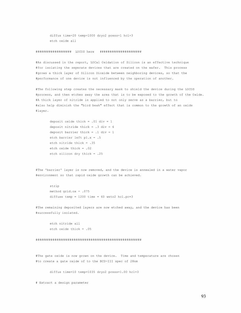
93
diffus time=20 temp=1000 dryo2 press=1 hcl=3
etch oxide all
################### LOCOS here ######################
#As discussed in the report, LOCal Oxidation of Silicon is an effective technique
#for isolating the seperate devices that are created on the wafer. This process
#grows a thick layer of Silicon Dioxide between neighboring devices, so that the
#performance of one device is not influenced by the operation of another.
#The following step creates the necessary mask to shield the device during the LOCOS
#process, and then etches away the area that is to be exposed to the growth of the Oxide.
#A thick layer of nitride is applied to not only serve as a barrier, but to
#also help diminish the "bird beak" effect that is common to the growth of an oxide
#layer.
deposit oxide thick = .01 div = 1
deposit nitride thick = .3 div = 6
deposit barrier thick = .1 div = 1
etch barrier left p1.x = .5
etch nitride thick = .35
etch oxide thick = .02
etch silicon dry thick = .25
#The 'barrier' layer is now removed, and the device is annealed in a water vapor
#environment so that rapid oxide growth can be achieved.
strip
method grid.ox = .075
diffuse temp = 1200 time = 60 weto2 hcl.pc=3
#The remaining deposited layers are now etched away, and the device has been
#successfully isolated.
etch nitride all
etch oxide thick = .05
########################################################
#The gate oxide is now grown on the device. Time and temperature are chosen
#to create a gate oxide of to the BCD-III spec of 28nm
diffus time=10 temp=1035 dryo2 press=1.00 hcl=3
# Extract a design parameter
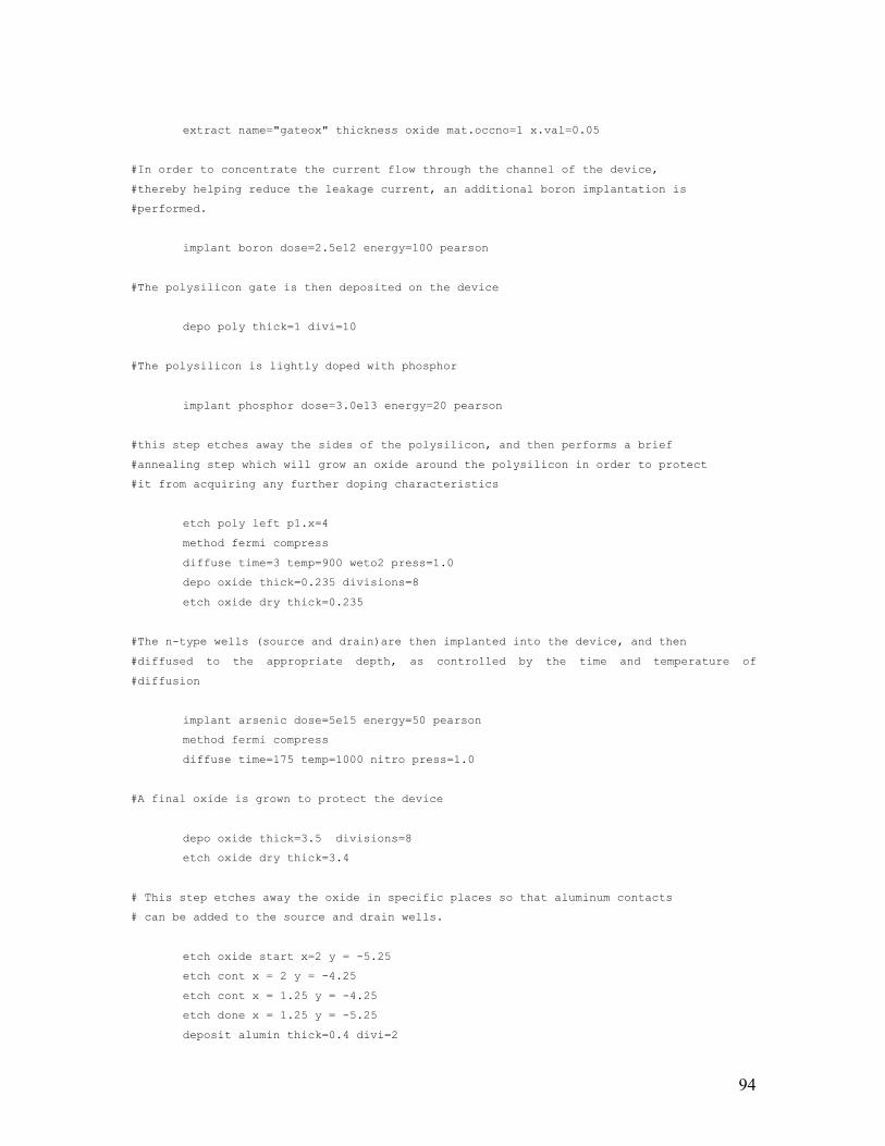
94
extract name="gateox" thickness oxide mat.occno=1 x.val=0.05
#In order to concentrate the current flow through the channel of the device,
#thereby helping reduce the leakage current, an additional boron implantation is
#performed.
implant boron dose=2.5e12 energy=100 pearson
#The polysilicon gate is then deposited on the device
depo poly thick=1 divi=10
#The polysilicon is lightly doped with phosphor
implant phosphor dose=3.0e13 energy=20 pearson
#this step etches away the sides of the polysilicon, and then performs a brief
#annealing step which will grow an oxide around the polysilicon in order to protect
#it from acquiring any further doping characteristics
etch poly left p1.x=4
method fermi compress
diffuse time=3 temp=900 weto2 press=1.0
depo oxide thick=0.235 divisions=8
etch oxide dry thick=0.235
#The n-type wells (source and drain)are then implanted into the device, and then
#diffused to the appropriate depth, as controlled by the time and temperature of
#diffusion
implant arsenic dose=5e15 energy=50 pearson
method fermi compress
diffuse time=175 temp=1000 nitro press=1.0
#A final oxide is grown to protect the device
depo oxide thick=3.5 divisions=8
etch oxide dry thick=3.4
# This step etches away the oxide in specific places so that aluminum contacts
# can be added to the source and drain wells.
etch oxide start x=2 y = -5.25
etch cont x = 2 y = -4.25
etch cont x = 1.25 y = -4.25
etch done x = 1.25 y = -5.25
deposit alumin thick=0.4 divi=2
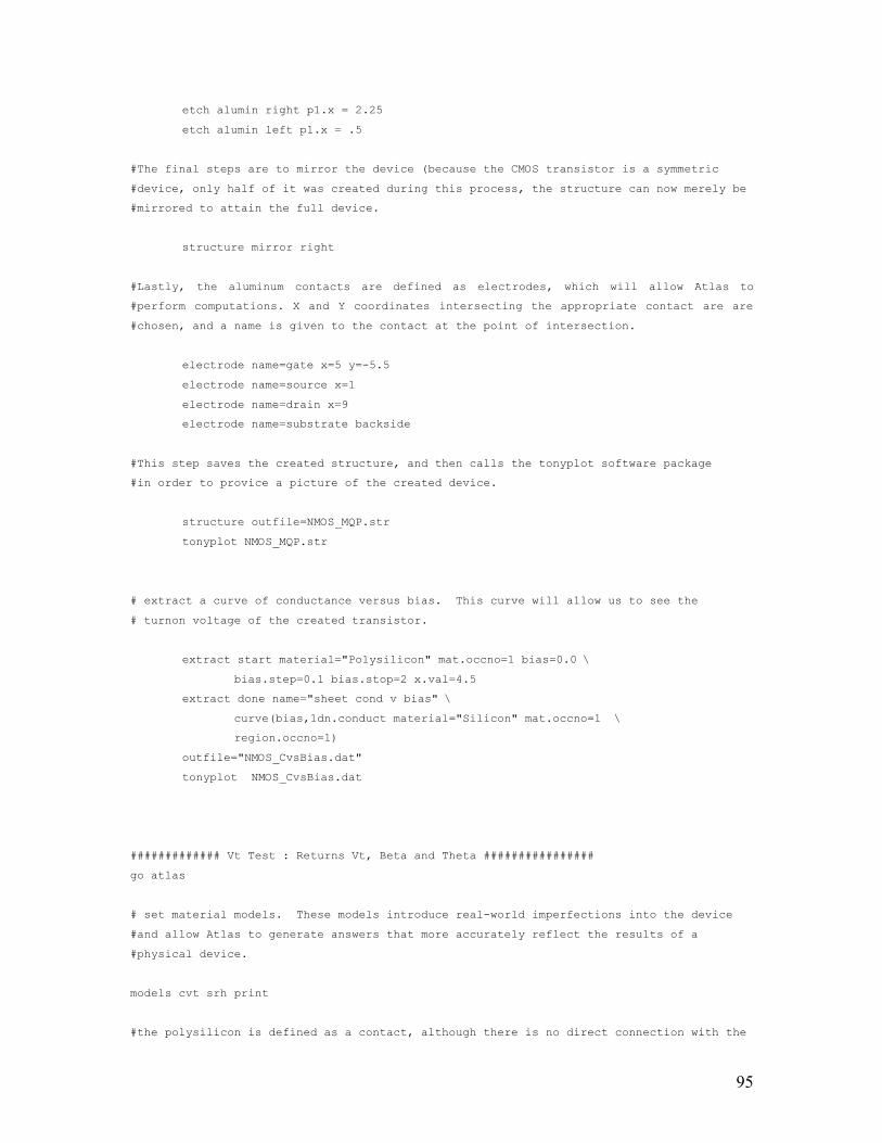
95
etch alumin right p1.x = 2.25
etch alumin left p1.x = .5
#The final steps are to mirror the device (because the CMOS transistor is a symmetric
#device, only half of it was created during this process, the structure can now merely be
#mirrored to attain the full device.
structure mirror right
#Lastly, the aluminum contacts are defined as electrodes, which will allow Atlas to
#perform computations. X and Y coordinates intersecting the appropriate contact are are
#chosen, and a name is given to the contact at the point of intersection.
electrode name=gate x=5 y=-5.5
electrode name=source x=1
electrode name=drain x=9
electrode name=substrate backside
#This step saves the created structure, and then calls the tonyplot software package
#in order to provice a picture of the created device.
structure outfile=NMOS_MQP.str
tonyplot NMOS_MQP.str
# extract a curve of conductance versus bias. This curve will allow us to see the
# turnon voltage of the created transistor.
extract start material="Polysilicon" mat.occno=1 bias=0.0 \
bias.step=0.1 bias.stop=2 x.val=4.5
extract done name="sheet cond v bias" \
curve(bias,1dn.conduct material="Silicon" mat.occno=1 \
region.occno=1)
outfile="NMOS_CvsBias.dat"
tonyplot NMOS_CvsBias.dat
############# Vt Test : Returns Vt, Beta and Theta ################
go atlas
# set material models. These models introduce real-world imperfections into the device
#and allow Atlas to generate answers that more accurately reflect the results of a
#physical device.
models cvt srh print
#the polysilicon is defined as a contact, although there is no direct connection with the
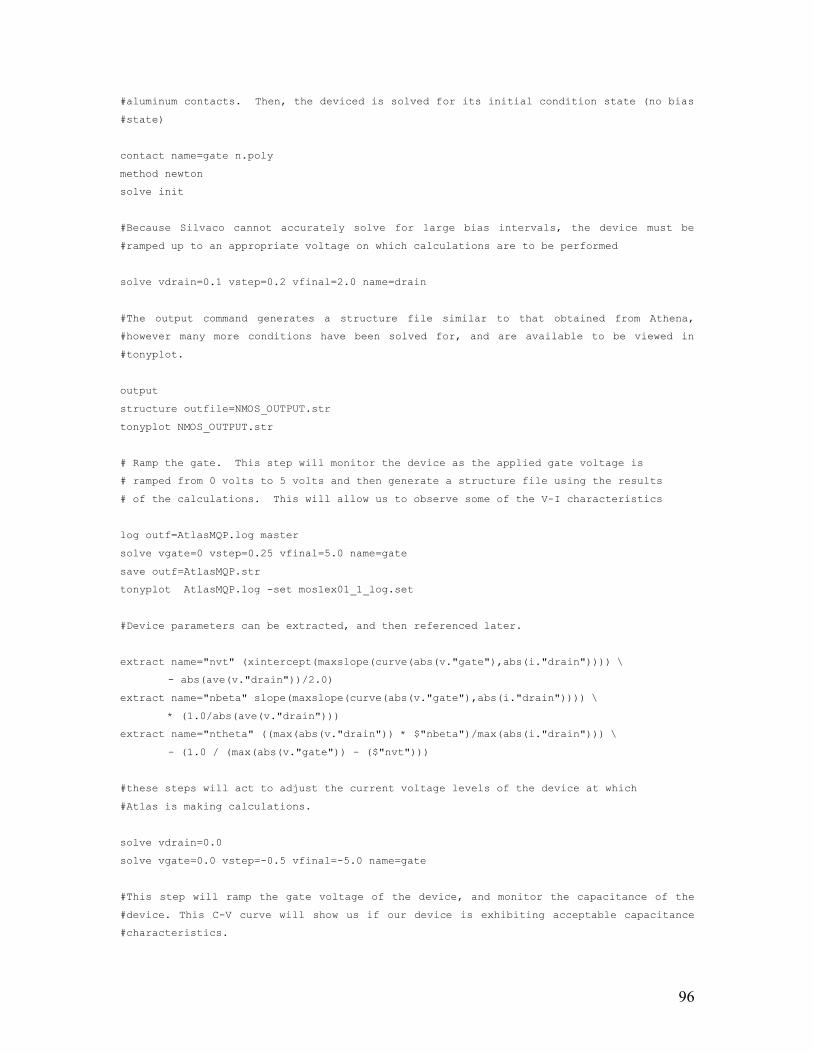
96
#aluminum contacts. Then, the deviced is solved for its initial condition state (no bias
#state)
contact name=gate n.poly
method newton
solve init
#Because Silvaco cannot accurately solve for large bias intervals, the device must be
#ramped up to an appropriate voltage on which calculations are to be performed
solve vdrain=0.1 vstep=0.2 vfinal=2.0 name=drain
#The output command generates a structure file similar to that obtained from Athena,
#however many more conditions have been solved for, and are available to be viewed in
#tonyplot.
output
structure outfile=NMOS_OUTPUT.str
tonyplot NMOS_OUTPUT.str
# Ramp the gate. This step will monitor the device as the applied gate voltage is
# ramped from 0 volts to 5 volts and then generate a structure file using the results
# of the calculations. This will allow us to observe some of the V-I characteristics
log outf=AtlasMQP.log master
solve vgate=0 vstep=0.25 vfinal=5.0 name=gate
save outf=AtlasMQP.str
tonyplot AtlasMQP.log -set mos1ex01_1_log.set
#Device parameters can be extracted, and then referenced later.
extract name="nvt" (xintercept(maxslope(curve(abs(v."gate"),abs(i."drain")))) \
- abs(ave(v."drain"))/2.0)
extract name="nbeta" slope(maxslope(curve(abs(v."gate"),abs(i."drain")))) \
* (1.0/abs(ave(v."drain")))
extract name="ntheta" ((max(abs(v."drain")) * $"nbeta")/max(abs(i."drain"))) \
- (1.0 / (max(abs(v."gate")) - ($"nvt")))
#these steps will act to adjust the current voltage levels of the device at which
#Atlas is making calculations.
solve vdrain=0.0
solve vgate=0.0 vstep=-0.5 vfinal=-5.0 name=gate
#This step will ramp the gate voltage of the device, and monitor the capacitance of the
#device. This C-V curve will show us if our device is exhibiting acceptable capacitance
#characteristics.
97
log outfile=mos2ex15_CV19_3.log
solve vgate=-5.0 vstep=0.1 vfinal=5.0 name=gate ac freq=1e0 previous
tonyplot mos2ex15_CV19_3.log -set mos2ex15_CV.set
#The following process will acquire three separate curves from the behavior of
#the device, and then plot them all on the same axes. The curves that we are
#generating are the drain current vs. drain voltage characteristics at three distinct
#gate voltage biases.
# set gate biases with Vds=0.0
solve vgate=1.5 outf=solve_tmp1
solve vgate=2.5 outf=solve_tmp2
solve vgate=3.5 outf=solve_tmp3
#load in temporary files and ramp Vds
load infile=solve_tmp1
log outf=GateVoltage_15.log
solve name=drain vdrain=0 vfinal=5.0 vstep=0.25
load infile=solve_tmp2
log outf=GateVoltage_25.log
solve name=drain vdrain=0 vfinal=5.0 vstep=0.25
load infile=solve_tmp3
log outf=GateVoltage_35.log
solve name=drain vdrain=0 vfinal=5.0 vstep=0.25
# extract max current and saturation slope
extract name="nidsmax" max(i."drain")
extract name="sat_slope" slope(minslope(curve(v."drain",i."drain")))
#tonyplot can graph multiple structures on the same axes, and that is what this step does
tonyplot -overlay -st GateVoltage_15.log GateVoltage_25.log GateVoltage_35.log
quit
98
Appendix C – PMOS Athena and Atlas Code go athena
#This initial step is used to define the mesh for the BCD structure. The mesh is
#important in determining on how many points of the device Athena will perform
#calculations. A mesh that is not dense enough will yield incorrect results, however a
#mesh that is too dense will require too many calculations and will make it impossible to
#run multiple simulations and quickly analyze results.
line x loc=0.0 spac=0.1
line x loc=1.66666 spac=0.05
line x loc=3.333333 spac=0.05
line x loc=5.0 spac=0.085
line y loc=0 spac=0.035
line y loc=1 spac=0.85
line y loc=5.0 spac=2.5
#The following line denotes the type of wafer on which the device is going to be
#constructed. For the CMOS devices, we will be using a silicon wafer, in a <100>
#orientation and doped with a boron level of 1e14
init orientation=100 c.boron=1e14 space.mul=2 TWO.D
#Here is where the arsenic epitaxial layer will be grown. Arsenic is chosen to create
#an n-type layer upon which the device will be constructed. The divisions parameter
#specifies the amount of new mesh layers to be applied to the newly grown epitaxial
#layer. The thickness is specified to be 4.5 micrometers (the default unit of length
#in Athena.
epitaxy time = 45 temp = 900 t.final = 1000 c.arsenic=1e16 \
thickness = 4.5 divisions = 20 \
dy = .05 ydy = 0.00
#As this is a PNP device, no Pwell infusion is necessary, as the epitaxial layer is NType
#arsenic
################### LOCOS here ######################
#As discussed in the report, LOCal Oxidation of Silicon is an effective technique
#for isolating the seperate devices that are created on the wafer. This process
#grows a thick layer of Silicon Dioxide between neighboring devices, so that the
#performance of one device is not influenced by the operation of another.
#The following step creates the necessary mask to shield the device during the LOCOS
#process, and then etches away the area that is to be exposed to the growth of the Oxide.
99
#A thick layer of nitride is applied to not only serve as a barrier, but to
#also help diminish the "bird beak" effect that is common to the growth of an oxide
#layer.
deposit oxide thick = .01 div = 1
deposit nitride thick = .3 div = 6
deposit barrier thick = .1 div = 1
etch barrier left p1.x = .5
etch nitride thick = .35
etch oxide thick = .02
etch silicon dry thick = .25
#The 'barrier' layer is now removed, and the device is annealed in a water vapor
#environment so that rapid oxide growth can be achieved.
strip
method grid.ox = .075
diffuse temp = 1200 time = 60 weto2 hcl.pc=3
#The remaining deposited layers are now etched away, and the device has been
#successfully isolated.
etch nitride all
etch oxide thick = .05
########################################################
#The gate oxide is now grown on the device. Time and temperature are chosen
#to create a gate oxide of to the BCD-III spec of 28nm
diffus time=10 temp=1035 dryo2 press=1.00 hcl=3
# Extract a design parameter
extract name="gateox" thickness oxide mat.occno=1 x.val=0.05
#In order to concentrate the current flow through the channel of the device,
#thereby helping reduce the leakage current, an additional arsenic implantation is
#performed.
implant arsenic dose=2.5e12 energy=250 pearson
#now that the channel is doped, the polysilicon can be deposited
depo poly thick=1 divi=10
#The polysilicon is lightly doped with phosphor
100
implant phosphor dose=3.0e13 energy=20 pearson
#this step etches away the sides of the polysilicon, and then performs a brief
#annealing step which will grow an oxide around the polysilicon in order to protect
#it from acquiring any further doping characteristics
etch poly left p1.x=4
method fermi compress
diffuse time=3 temp=900 weto2 press=1.0
depo oxide thick=0.235 divisions=8
etch oxide dry thick=0.235
#The p-type wells (source and drain) are then implanted into the device, and then
#diffused to the appropriate depth, as controlled by the time and temperature of
#diffusion
implant boron dose=5e15 energy=25 pearson
method fermi compress
diffuse time=390 temp=925 nitro press=1.0
#A final oxide is grown to protect the device
depo oxide thick=3.5
etch oxide dry thick=3.4
# This step etches away the oxide in specific places so that aluminum contacts
# can be added to the source and drain wells.
etch oxide start x=2 y = -6.25
etch cont x = 2 y = -4.25
etch cont x = 1.25 y = -4.25
etch done x = 1.25 y = -6.25
deposit alumin thick=0.4 divi=2
etch alumin right p1.x = 2.25
etch alumin left p1.x = .5
#The final steps are to mirror the device (because the CMOS transistor is a symmetric
#device, only half of it was created during this process, the structure can now merely be
#mirrored to attain the full device.
structure mirror right
#Lastly, the aluminum contacts are defined as electrodes, which will allow Atlas to
#perform computations. X and Y coordinates intersecting the appropriate contact are are
#chosen, and a name is given to the contact at the point of intersection.
electrode name=gate x=5 y=-5.5
electrode name=source x=1
101
electrode name=drain x=9
electrode name=substrate backside
#This step saves the created structure, and then calls the tonyplot software package
#in order to provice a picture of the created device.
structure outfile=PMOS_MQP.str
tonyplot PMOS_MQP.str
# extract a curve of conductance versus bias.
extract start material="Polysilicon" mat.occno=1 \
bias=0.0 bias.step=-0.1 bias.stop=-5 x.val=4.5
extract done name="sheet cond v bias" \
curve(bias,1dn.conduct material="Silicon" mat.occno=1 \
region.occno=1)
outfile="PMOS_CvsBias.dat"
tonyplot PMOS_CvsBias.dat
structure outfile=PMOS_MQP.str
# plot the structure
tonyplot PMOS_MQP.str -set mos1ex01_0.set
###################################################################
go atlas
# set material models. These models introduce real-world imperfections into the device
#and allow Atlas to generate answers that more accurately reflect the results of a
#physical device. srh = shockley-reed-hall, and governs the minority carrier
#recombination rate. cvt = Lombardi Model for N, G, E// and E (perpendicular) effects
models cvt srh print
#the polysilicon is defined as a contact, although there is no direct connection with the
#aluminum contacts. Then, the deviced is solved for its initial condition state (no bias
#state)
contact name=gate n.poly
method newton
solve init
#Because Silvaco cannot accurately solve for large bias intervals, the device must be
#ramped up to an appropriate voltage on which calculations are to be performed
solve vdrain=0.1 vstep=-0.2 vfinal=-2.0 name=drain
102
#The output command generates a structure file similar to that obtained from Athena,
#however many more conditions have been solved for, and are available to be viewed in
#tonyplot.
output
structure outfile=PMOS_OUTPUT.str
tonyplot PMOS_OUTPUT.str
# Ramp the gate. This step will monitor the device as the applied gate voltage is
# ramped from 0 volts to -5 volts and then generate a structure file using the results
# of the calculations. This will allow us to observe some of the V-I characteristics
log outf=AtlasMQP.log master
solve vgate=0 vstep=-0.25 vfinal=-5.0 name=gate
save outf=AtlasMQP.str
tonyplot AtlasMQP.log -set mos1ex01_1_log.set
# extract device parameters
extract name="nvt" (xintercept(maxslope(curve(abs(v."gate"),abs(i."drain")))) \
- abs(ave(v."drain"))/2.0)
extract name="nbeta" slope(maxslope(curve(abs(v."gate"),abs(i."drain")))) \
* (1.0/abs(ave(v."drain")))
extract name="ntheta" ((max(abs(v."drain")) * $"nbeta")/max(abs(i."drain"))) \
- (1.0 / (max(abs(v."gate")) - ($"nvt")))
#these steps will act to adjust the current voltage levels of the device at which
#Atlas is making calculations.
solve vdrain=0.0
solve vgate=0.0 vstep = -.5 vfinal = -5.0 name = gate
#This step will ramp the gate voltage of the device, and monitor the capacitance of the
#device. This C-V curve will show us if our device is exhibiting acceptable capacitance
#characteristics.
log outfile=mos2ex15_CV19.log
solve vgate=-5.0 vstep=0.5 vfinal=5.0 name=gate ac freq=1e1 previous
tonyplot mos2ex15_CV19.log -set mos2ex15_CV.set
#The following process will acquire three separate curves from the behavior of
#the device, and then plot them all on the same axes. The curves that we are
#generating are the drain current vs. drain voltage characteristics at three distinct
#gate voltage biases.
# set gate biases with Vds=0.0
103
solve vgate=-1.5 outf=solve_tmp1
solve vgate=-2.5 outf=solve_tmp2
solve vgate=-3.5 outf=solve_tmp3
#load in temporary files and ramp Vds
load infile=solve_tmp1
log outf=mos1ex02_1.log
solve name=drain vdrain=0 vfinal=-5.0 vstep=-0.25
load infile=solve_tmp2
log outf=mos1ex02_2.log
solve name=drain vdrain=0 vfinal=-5.0 vstep=-0.25
load infile=solve_tmp3
log outf=mos1ex02_3.log
solve name=drain vdrain=0 vfinal=-5.0 vstep=-0.25
# extract max current and saturation slope
extract name="nidsmax" max(i."drain")
extract name="sat_slope" slope(minslope(curve(v."drain",i."drain")))
#tonyplot can graph multiple structures on the same axes, and that is what this step does
tonyplot -overlay -st mos1ex02_1.log mos1ex02_2.log mos1ex02_3.log -set mos1ex02_1.set
quit
104
Appendix D – BJT Athena and Atlas Code go athena
#This initial step is used to define the mesh for the BCD structure. The mesh is
#important in determining on how many points of the device Athena will perform
#calculations. A mesh that is not dense enough will yield incorrect results, however a
#mesh that is too dense will require too many calculations and will make it impossible to
#run multiple simulations and quickly analyze results.
line x loc=0.0 spac=0.05
line x loc=5.0 spac=0.05
line y loc=0 spac=0.1
line y loc=2 spac=0.50
line y loc=5.0 spac=2
#The following line denotes the type of wafer on which the device is going to be
#constructed. For the CMOS devices, we will be using a silicon wafer, in a <100>
#orientation and doped with a boron level of 1e14
init orientation=100 c.boron=1e14 space.mul=2 TWO.D
#Here is where the arsenic epitaxial layer will be grown. Arsenic is chosen to create
#an n-type layer upon which the device will be constructed. The divisions parameter
#specifies the amount of new mesh layers to be applied to the newly grown epitaxial
#layer. The thickness is specified to be 4.5 micrometers (the default unit of length
#in Athena.
epitaxy time = 45 temp = 900 t.final = 1000 c.arsenic=1e16 \
thickness = 4.5 divisions = 25 dy = .05 ydy = 0.00
################### LOCOS is here #########
#As discussed in the report, LOCal Oxidation of Silicon is an effective technique
#for isolating the seperate devices that are created on the wafer. This process
#grows a thick layer of Silicon Dioxide between neighboring devices, so that the
#performance of one device is not influenced by the operation of another.
#The following step creates the necessary mask to shield the device during the LOCOS
#process, and then etches away the area that is to be exposed to the growth of the Oxide.
#A thick layer of nitride is applied to not only serve as a barrier, but to
#also help diminish the "bird beak" effect that is common to the growth of an oxide
#layer. This code remains commented as the dimensions have not been finalized, due to
#our focus on the device operation. The process as described below is correct in all
#aspects except the etching coordinates.
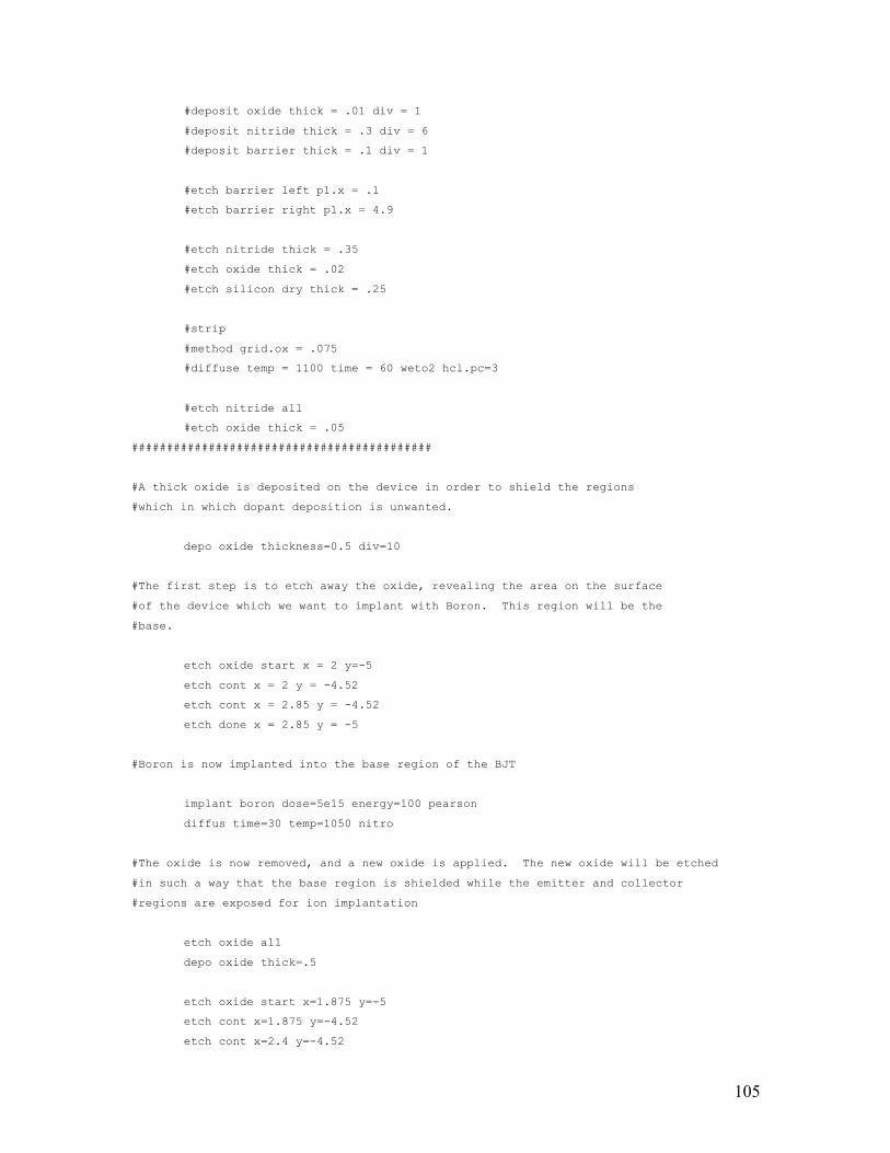
105
#deposit oxide thick = .01 div = 1
#deposit nitride thick = .3 div = 6
#deposit barrier thick = .1 div = 1
#etch barrier left p1.x = .1
#etch barrier right p1.x = 4.9
#etch nitride thick = .35
#etch oxide thick = .02
#etch silicon dry thick = .25
#strip
#method grid.ox = .075
#diffuse temp = 1100 time = 60 weto2 hcl.pc=3
#etch nitride all
#etch oxide thick = .05
###########################################
#A thick oxide is deposited on the device in order to shield the regions
#which in which dopant deposition is unwanted.
depo oxide thickness=0.5 div=10
#The first step is to etch away the oxide, revealing the area on the surface
#of the device which we want to implant with Boron. This region will be the
#base.
etch oxide start x = 2 y=-5
etch cont x = 2 y = -4.52
etch cont x = 2.85 y = -4.52
etch done x = 2.85 y = -5
#Boron is now implanted into the base region of the BJT
implant boron dose=5e15 energy=100 pearson
diffus time=30 temp=1050 nitro
#The oxide is now removed, and a new oxide is applied. The new oxide will be etched
#in such a way that the base region is shielded while the emitter and collector
#regions are exposed for ion implantation
etch oxide all
depo oxide thick=.5
etch oxide start x=1.875 y=-5
etch cont x=1.875 y=-4.52
etch cont x=2.4 y=-4.52
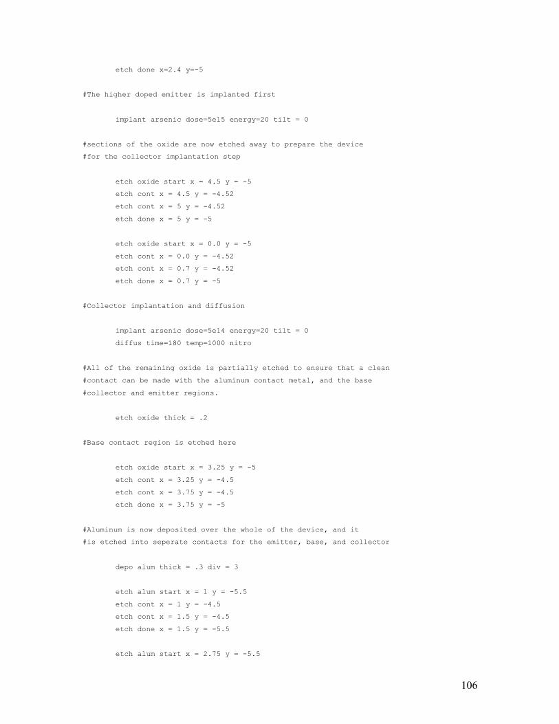
106
etch done x=2.4 y=-5
#The higher doped emitter is implanted first
implant arsenic dose=5e15 energy=20 tilt = 0
#sections of the oxide are now etched away to prepare the device
#for the collector implantation step
etch oxide start x = 4.5 y = -5
etch cont x = 4.5 y = -4.52
etch cont x = 5 y = -4.52
etch done x = 5 y = -5
etch oxide start x = 0.0 y = -5
etch cont x = 0.0 y = -4.52
etch cont x = 0.7 y = -4.52
etch done x = 0.7 y = -5
#Collector implantation and diffusion
implant arsenic dose=5e14 energy=20 tilt = 0
diffus time=180 temp=1000 nitro
#All of the remaining oxide is partially etched to ensure that a clean
#contact can be made with the aluminum contact metal, and the base
#collector and emitter regions.
etch oxide thick = .2
#Base contact region is etched here
etch oxide start x = 3.25 y = -5
etch cont x = 3.25 y = -4.5
etch cont x = 3.75 y = -4.5
etch done x = 3.75 y = -5
#Aluminum is now deposited over the whole of the device, and it
#is etched into seperate contacts for the emitter, base, and collector
depo alum thick = .3 div = 3
etch alum start x = 1 y = -5.5
etch cont x = 1 y = -4.5
etch cont x = 1.5 y = -4.5
etch done x = 1.5 y = -5.5
etch alum start x = 2.75 y = -5.5
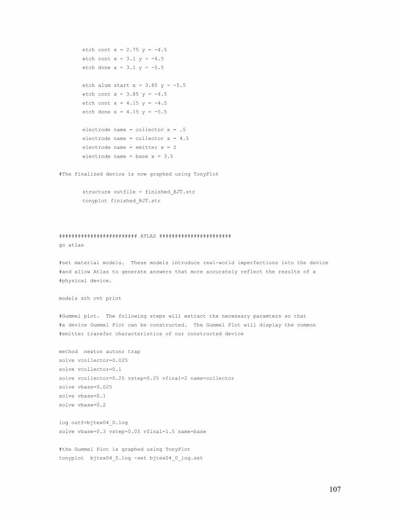
107
etch cont x = 2.75 y = -4.5
etch cont x = 3.1 y = -4.5
etch done x = 3.1 y = -5.5
etch alum start x = 3.85 y = -5.5
etch cont x = 3.85 y = -4.5
etch cont x = 4.15 y = -4.5
etch done x = 4.15 y = -5.5
electrode name = collector x = .5
electrode name = collector x = 4.5
electrode name = emitter x = 2
electrode name = base x = 3.5
#The finalized device is now graphed using TonyPlot
structure outfile = finished_BJT.str
tonyplot finished_BJT.str
######################### ATLAS #######################
go atlas
#set material models. These models introduce real-world imperfections into the device
#and allow Atlas to generate answers that more accurately reflect the results of a
#physical device.
models srh cvt print
#Gummel plot. The following steps will extract the necessary paramters so that
#a device Gummel Plot can be constructed. The Gummel Plot will display the common
#emitter transfer characteristics of our constructed device
method newton autonr trap
solve vcollector=0.025
solve vcollector=0.1
solve vcollector=0.25 vstep=0.25 vfinal=2 name=collector
solve vbase=0.025
solve vbase=0.1
solve vbase=0.2
log outf=bjtex04_0.log
solve vbase=0.3 vstep=0.05 vfinal=1.5 name=base
#the Gummel Plot is graphed using TonyPlot
tonyplot bjtex04_0.log -set bjtex04_0_log.set
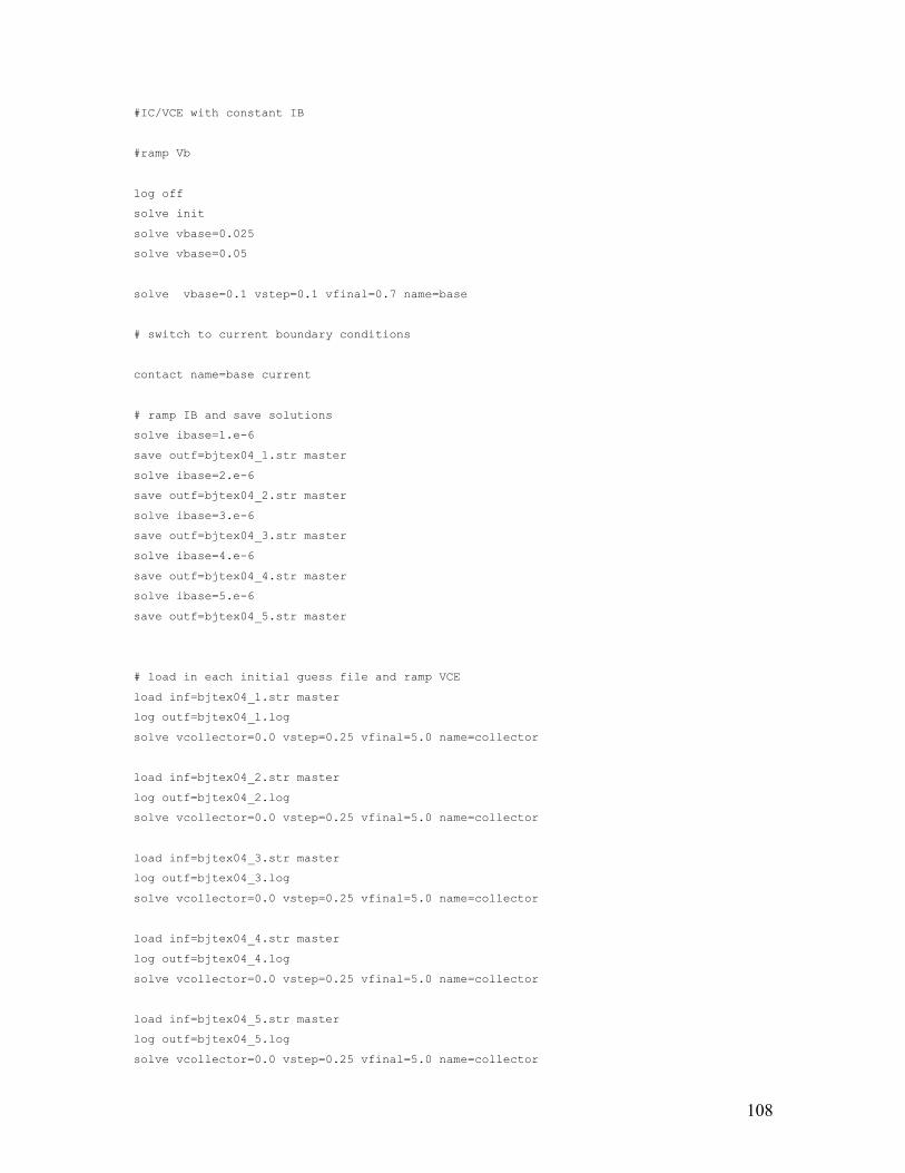
108
#IC/VCE with constant IB
#ramp Vb
log off
solve init
solve vbase=0.025
solve vbase=0.05
solve vbase=0.1 vstep=0.1 vfinal=0.7 name=base
# switch to current boundary conditions
contact name=base current
# ramp IB and save solutions
solve ibase=1.e-6
save outf=bjtex04_1.str master
solve ibase=2.e-6
save outf=bjtex04_2.str master
solve ibase=3.e-6
save outf=bjtex04_3.str master
solve ibase=4.e-6
save outf=bjtex04_4.str master
solve ibase=5.e-6
save outf=bjtex04_5.str master
# load in each initial guess file and ramp VCE
load inf=bjtex04_1.str master
log outf=bjtex04_1.log
solve vcollector=0.0 vstep=0.25 vfinal=5.0 name=collector
load inf=bjtex04_2.str master
log outf=bjtex04_2.log
solve vcollector=0.0 vstep=0.25 vfinal=5.0 name=collector
load inf=bjtex04_3.str master
log outf=bjtex04_3.log
solve vcollector=0.0 vstep=0.25 vfinal=5.0 name=collector
load inf=bjtex04_4.str master
log outf=bjtex04_4.log
solve vcollector=0.0 vstep=0.25 vfinal=5.0 name=collector
load inf=bjtex04_5.str master
log outf=bjtex04_5.log
solve vcollector=0.0 vstep=0.25 vfinal=5.0 name=collector

109
# plot results
tonyplot -overlay bjtex04_1.log bjtex04_2.log bjtex04_3.log bjtex04_4.log bjtex04_5.log
-set bjtex04_1_log.set
quit
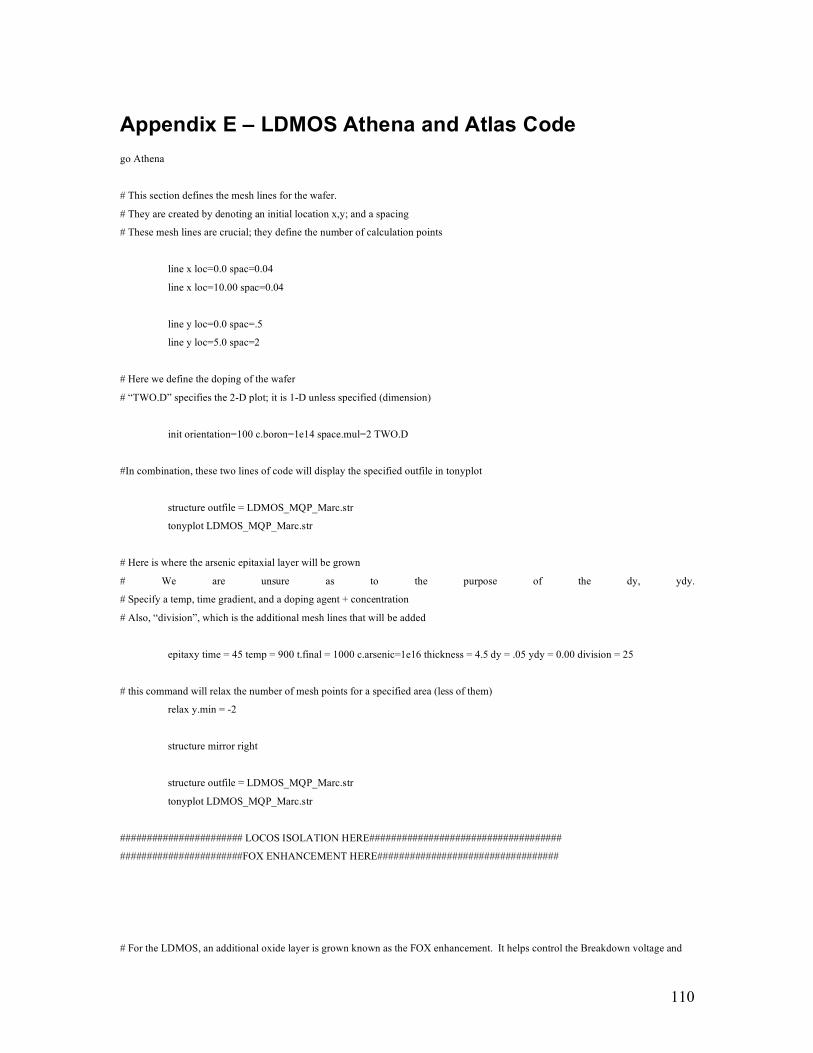
110
Appendix E – LDMOS Athena and Atlas Code go Athena
# This section defines the mesh lines for the wafer.
# They are created by denoting an initial location x,y; and a spacing
# These mesh lines are crucial; they define the number of calculation points
line x loc=0.0 spac=0.04
line x loc=10.00 spac=0.04
line y loc=0.0 spac=.5
line y loc=5.0 spac=2
# Here we define the doping of the wafer
# “TWO.D” specifies the 2-D plot; it is 1-D unless specified (dimension)
init orientation=100 c.boron=1e14 space.mul=2 TWO.D
#In combination, these two lines of code will display the specified outfile in tonyplot
structure outfile = LDMOS_MQP_Marc.str
tonyplot LDMOS_MQP_Marc.str
# Here is where the arsenic epitaxial layer will be grown
# We are unsure as to the purpose of the dy, ydy.
# Specify a temp, time gradient, and a doping agent + concentration
# Also, “division”, which is the additional mesh lines that will be added
epitaxy time = 45 temp = 900 t.final = 1000 c.arsenic=1e16 thickness = 4.5 dy = .05 ydy = 0.00 division = 25
# this command will relax the number of mesh points for a specified area (less of them)
relax y.min = -2
structure mirror right
structure outfile = LDMOS_MQP_Marc.str
tonyplot LDMOS_MQP_Marc.str
####################### LOCOS ISOLATION HERE####################################
#######################FOX ENHANCEMENT HERE##################################
# For the LDMOS, an additional oxide layer is grown known as the FOX enhancement. It helps control the Breakdown voltage and
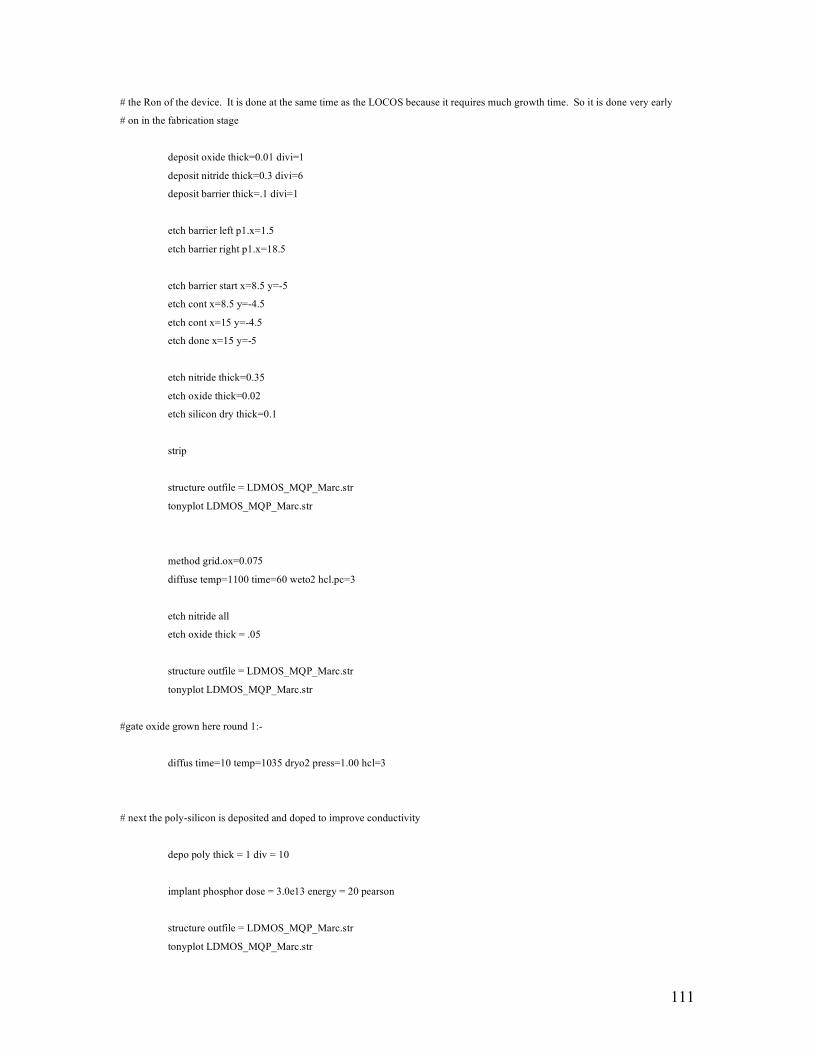
111
# the Ron of the device. It is done at the same time as the LOCOS because it requires much growth time. So it is done very early
# on in the fabrication stage
deposit oxide thick=0.01 divi=1
deposit nitride thick=0.3 divi=6
deposit barrier thick=.1 divi=1
etch barrier left p1.x=1.5
etch barrier right p1.x=18.5
etch barrier start x=8.5 y=-5
etch cont x=8.5 y=-4.5
etch cont x=15 y=-4.5
etch done x=15 y=-5
etch nitride thick=0.35
etch oxide thick=0.02
etch silicon dry thick=0.1
strip
structure outfile = LDMOS_MQP_Marc.str
tonyplot LDMOS_MQP_Marc.str
method grid.ox=0.075
diffuse temp=1100 time=60 weto2 hcl.pc=3
etch nitride all
etch oxide thick = .05
structure outfile = LDMOS_MQP_Marc.str
tonyplot LDMOS_MQP_Marc.str
#gate oxide grown here round 1:-
diffus time=10 temp=1035 dryo2 press=1.00 hcl=3
# next the poly-silicon is deposited and doped to improve conductivity
depo poly thick = 1 div = 10
implant phosphor dose = 3.0e13 energy = 20 pearson
structure outfile = LDMOS_MQP_Marc.str
tonyplot LDMOS_MQP_Marc.str
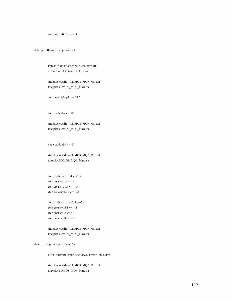
112
etch poly left p1.x = 4.5
# the p-well drive is implemented
implant boron dose = 5e15 energy = 100
diffus time=150 temp=1100 nitro
structure outfile = LDMOS_MQP_Marc.str
tonyplot LDMOS_MQP_Marc.str
etch poly right p1.x = 13.5
etch oxide thick = .05
structure outfile = LDMOS_MQP_Marc.str
tonyplot LDMOS_MQP_Marc.str
depo oxide thick = .5
structure outfile = LDMOS_MQP_Marc.str
tonyplot LDMOS_MQP_Marc.str
etch oxide start x=4 y=-5.5
etch cont x=4 y = -4.4
etch cont x=2.25 y = -4.4
etch done x=2.25 y = -5.5
etch oxide start x=15.5 y=-5.5
etch cont x=15.5 y=-4.4
etch cont x=18 y=-4.4
etch done x=18 y=-5.5
structure outfile = LDMOS_MQP_Marc.str
tonyplot LDMOS_MQP_Marc.str
#gate oxide grown here round 2:-
diffus time=10 temp=1035 dryo2 press=1.00 hcl=3
structure outfile = LDMOS_MQP_Marc.str
tonyplot LDMOS_MQP_Marc.str
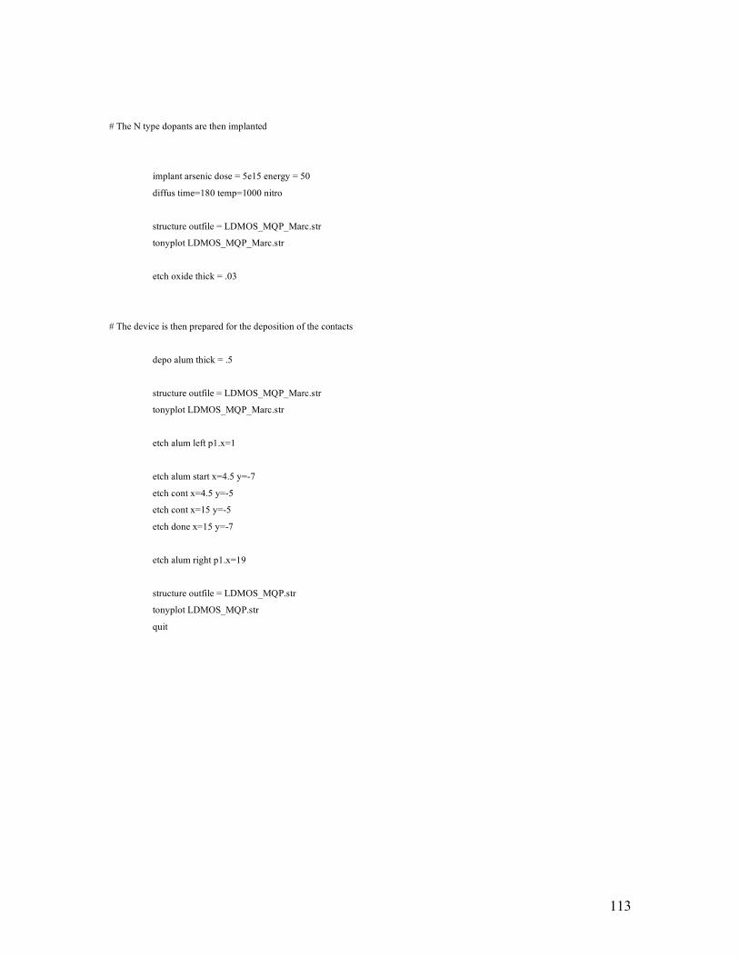
113
# The N type dopants are then implanted
implant arsenic dose = 5e15 energy = 50
diffus time=180 temp=1000 nitro
structure outfile = LDMOS_MQP_Marc.str
tonyplot LDMOS_MQP_Marc.str
etch oxide thick = .03
# The device is then prepared for the deposition of the contacts
depo alum thick = .5
structure outfile = LDMOS_MQP_Marc.str
tonyplot LDMOS_MQP_Marc.str
etch alum left p1.x=1
etch alum start x=4.5 y=-7
etch cont x=4.5 y=-5
etch cont x=15 y=-5
etch done x=15 y=-7
etch alum right p1.x=19
structure outfile = LDMOS_MQP.str
tonyplot LDMOS_MQP.str
quit