selective electroless nickel and gold plating of · pdf file · 2011-10-22selective...
TRANSCRIPT
Selective Electroless Nickel and Gold Plating of Individual Integrated Circuits for
Thermocompression Gold Stud Bump Flip-Chip Attachment
David M Lee Eldwin L Dodson and Guy V Clatterbaugh
Johns Hopkins University Applied Physics Laboratory
Laurel Maryland
Abstract
Flip chip bonding is the most desirable direct chip attachment approach for minimizing electronic assembly size as well as
improving device performance For most prototyping applications it is not cost-effective to purchase individual integrated circuits
(ICs) that are solder-bumped as this typically requires the purchase of entire wafer Also many unpackaged ICrsquos in die form are
not available for purchase as an entire wafer for subsequent solder bumping As an alternative to solder bumping manufacturers
of wire bond equipment have developed the gold stud bump process which allows single ICrsquos to be automatically bumped using
1-mil gold wire However the rapid formation of brittle aluminum-gold (Al-Au) intermetallics at elevated temperatures (gt200oC)
precludes the use of thermocompression flip chip bonding due to the unreliability of the bond at the IC pad interface To
overcome the intermetallic problem at the ICs aluminum-metallized bonding pads an electroless nickel and gold plating process
was developed for making a gold-bondable diffusion barrier for use on individual unpackaged silicon ICrsquos This process
provided an electroless gold layer suitable for accepting the gold wire stud bumps as well as providing the necessary barrier to Al-
Au intermetallic formation A number of experiments were conducted using electroless nickel of various phosphorus contents to
determine which would provide an optimal diffusion layer Data will be presented comparing immersion and autocatalytic gold
plating processes Test wafers were stud-bumped and exposed to accelerated temperatures then shear tested Electroless nickel
immersion and autocatalytic gold plating process parameters were optimized to provide high reliability interconnections when
using the high temperature thermocompression flip-chip bonding die-attach method
Introduction
The gold stud bump flip chip process creates gold bumps on integrated circuit (IC) die bond pads The die is then directly
connected to a circuit board or substrate Gold stud bumps are formed by a wire bonder utilizing a modified wire bonding
technique This process allows individual off the shelf die to be gold stud bumped This process is ideal for product
development and prototyping
Aluminum is generally the metallization used for IC bond pads Flip chip bonding of gold stud-bumped chips can be
accomplished using an anisotropic adhesive or by thermocompression bonding Thermocompression bonding is a much faster
than waiting for anisotropic adhesive to cure However bonds made with stud bumps that are made directly on aluminum bond
pads are unreliable due to the aluminum-gold intermetallics that form readily at thermocompression bonding temperatures
(~300oC) It well known that the formation of aluminum-gold (Al-Au) intermetallics at elevated temperatures (gt200
oC) degrades
and compromises the bond at the gold bump and aluminum pad interface
A number of Under Bump Metallization (UBM) processes have been developed to overcome the intermetallic formation UBM
may be vacuum deposited by evaporation and sputtering techniques or electroless and immersion plating processes However
vacuum deposition would is not suitable for metalizing individual die because of the number of masking steps they require
Electroless plating is an ideal alternative to vacuum deposition This paper discusses an electroless nickel immersion and
autocatalytic gold plating process that was developed to plate aluminum bond pads on individual ICrsquos
Background
When electroless nickel and gold (ENIG) plating aluminum a zincation process is used to activate the exposed aluminum before
the nickel is deposited The aluminum oxide layer is removed and the surface is activated through zinc displacement plating using
a zincate solution A double-zincation process is used to assure maximum adhesion Electroless nickel (EN) is then deposited
from a hypophosphate-based nickel bath The EN is an autocatalytic process which chemically deposits a nickel-phosphorus alloy
onto the zincated aluminum The phosphorus content of EN baths can range from 3 up to 15 Immersion gold is then
deposited thru a galvanic reaction with the electroless nickel to deposit a thin layer of gold onto the nickel For applications that
require a thick gold layer such as stud bumping and wire bonding autocatalytic electroless gold is then plated over the immersion
gold layer
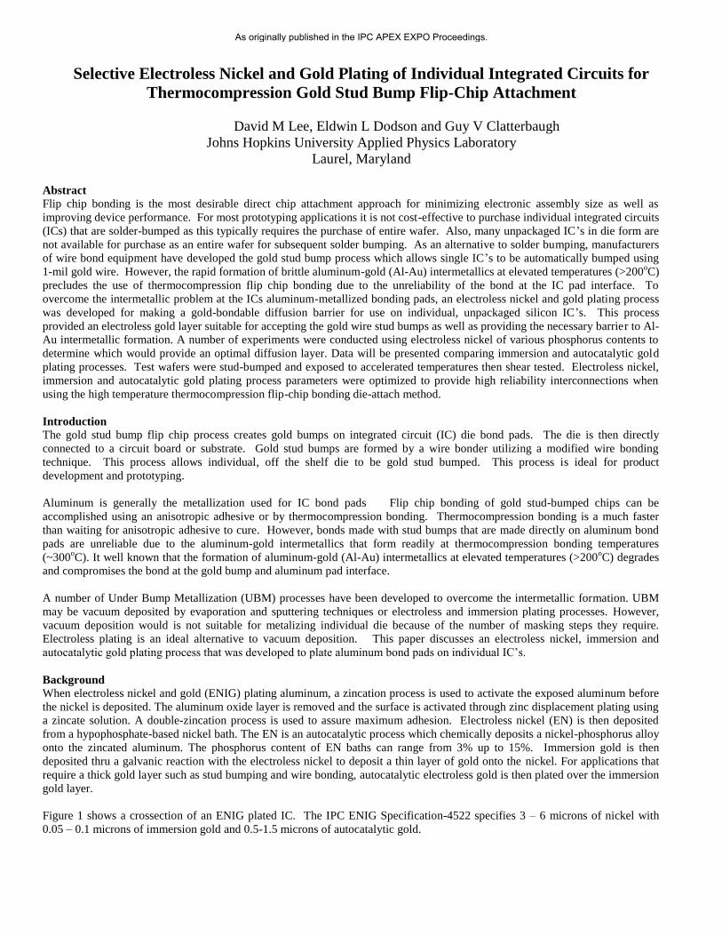
Figure 1 shows a crossection of an ENIG plated IC The IPC ENIG Specification-4522 specifies 3 ndash 6 microns of nickel with
005 ndash 01 microns of immersion gold and 05-15 microns of autocatalytic gold
As originally published in the IPC APEX EXPO Proceedings
Figure 1- Cross-section of plated IC
Since all ICrsquos are not fabricated the same way ENIG plating process steps have to be tailored to each individual IC type
Variations in the aluminum alloy bond pad size and thickness passivation material and bond pad electrical potential have to be
analyzed Probe marks on bond pads and contamination also can make plating difficult
Experimental Procedure
A number of plating companies offer proprietary processes for ENIG plating on aluminum The plating experiments in this paper
were conducted using one of these proprietary processes EN baths containing phosphorus contents of 2-3 7-8 and 11-12
were compared EN deposits with both immersion and autocatalytic gold were evaluated The pre-plate preparation steps plating
times and metal layer composition were varied The adhesion strength of the ENIG layers was evaluated by measuring the force
required to shear gold stud bumps from the plated aluminum pads The reliability of the stud bump-to-plated pad interface was
evaluated using a ball shear test after subjecting test vehicles to multiple temperature cycles and high temperature dwells
Silicon wafers with 2 microns of evaporated aluminum were prepared as test coupons The wafers were annealed at 200oC for 2
hours to increase the adhesion of the aluminum The wafers were then diced into 1x1rdquo test coupons The silicon coupons were
plated before the individual ICrsquos to analyze the plating processes
The process steps for the ENIG under-bump metallization are shown in Table 1 The first step is a plasma etch in an oxygenargon
plasma The plasma etching removes surface organics The coupons are then immersed in a cleaner to remove any contaminates
and help the wetting process A micro etch is used to break down the oxide layer and to remove any alloying constituents from the
surface of the aluminum A nitric acid dip re-forms the oxide layer and prepares the aluminum to accept the zinc A double-
zincation process is used to obtain a uniform zinc layer and to assure maximum adhesion Each wet process step is followed by a
rinse in de-ionized water The test coupons were plated with 4 microns of nickel and 005 ndash 01 microns of immersion gold
Coupons were also prepared with 1 micron of autocatalytic gold
Table 1 Process Steps
The test coupons were plated with each of the conditions listed in Table 2 Each coupon was then gold stud bumped with 40
bumps using a FampK 6400 Wire Bonder with the following parameters 1 mil gold wire time = 30 bond force = 30 and ultrasonic
power = 110 The coupons were subjected to a die shear test using a Dage Series 4000 Bondtester with the following parameters
speed 1500mils shear height 010mil The bumping parameters were kept consent for all samples in this experiment
It was decided that 20 grams-force would constitute the minimum value acceptable for an individual stud bump shear strength
The silicon coupons were first shear-tested ldquoas platedrdquo The shear results were listed in 3 categories
lt20 g = poor 20-40g = acceptable and gt40g = good
1) Plasma Etch 6) 2nd
Nitric Acid Dip
2) Cleaner 7) 2nd
Zincate
3) Micro Etch 8) Electroless Nickel
4) 1st Nitric Acid Dip 9) Immersion Gold
5) 1st Zincate 10) Autocatalytic Gold
As originally published in the IPC APEX EXPO Proceedings
Table 2 indicates poor adhesion for the 2-3 phosphorus nickel regardless of the gold thickness For this case there was no
measurable adhesion at the nickelimmersion gold interface The 7-8 and the 11-12 phosphorus nickel have poor adhesion
with the immersion gold but had very good adhesion with the thicker autocatalytic gold
Table 2- STUD BUMP ADHESION
Coupons from the two plating processes that passed the ldquoas platedrdquo test were then subjected to a thermal soak consisting of 1 hour
at 300oC followed by 168 hours at 150
oC The 7-8 phosphorus nickelautocatalytic gold showed no degradation in bond strength
after the temperature soak The 11-12 phosphorus nickelautocatalytic gold showed a loss in of adhesion but the bonds could
still be categorized as acceptable as shown in Table 3 The two suitable plating baths were investigated and compared in the
following plating tests
Two types of ICrsquos were selected for this experiment and are shown in Figures 2 and 3 IC-A is a Voltage Regulator using bipolar
technology IC-B is a Memory Chip using C-MOS technology Each IC was from a different manufacturer IC-A bond pads are
100x100 microns and the aluminum is 2 microns thick The passivation layer is 2 microns IC-B bond pads are 125x125 microns
and the aluminum is 2 microns thick The passivation layer is 2 microns
Figure 2 -IC-A
ENIG PLATING STUDIED As Plated 1 HOUR 300oC 168 hours 150
oC
2-3 Phosphorus NickelImmersion Gold Poor
2-3 Phosphorus NickelImmersion GoldAutocatalytic Gold Poor
7-8 Phosphorus NickelImmersion Gold Poor
7-8 Phosphorus NickelImmersion Gold Autocatalytic Gold Good Good Good
11-12 Phosphorus NickelImmersion Gold Poor
11-12 Phosphorus NickelImmersion Gold Autocatalytic Gold Good Acceptable Acceptable
Table 3 Adhesion test
0102030405060708090
As Plated 1 Hour
300C
168 Hours
150C
Sh
ear
Fo
rce (
g)
7-8P 11-12P
As originally published in the IPC APEX EXPO Proceedings
Figure 3-IC-B
The back and sides of each IC was coated with liquid resist to prevent unwanted plating on any metalized areas except the bond
pads The ICrsquos were ENIG plated with the process shown in Table 1 Electroless nickel layers of 4 microns were deposited on
each specimen The electroless nickel baths containing 7-8 and 11-12 phosphorous was compared Immersion gold layers of
005 ndash 01 microns were deposited followed by a 1 micron deposition of autocatalytic gold
The nickel and gold thicknesses were determined by using Seiko Instrumentrsquos SFT 7000 Fluorescence X-Ray Gauge Figures 4
and 5 show a bond pad both before and after plating respectively
Figure 4-Before ENIG Figure 5-After ENIG
Process Issues
A number of processing problems were encountered when plating the IC specimens As mentioned earlier surface preparation is
a critical step in preparing the aluminum for the zincate step Also the etching step must be carefully controlled The amount of
time to etch and the concentration of the etchant are dictated by the aluminum alloy and thickness Figure 6 shows bond pads that
have been over etched The dark pits are largely copper that is added to the aluminum to retard the solid-state diffusion of gold
into aluminum
Figure 6-Overetched pads
Uneven plating can occur if a non uniform zincation layer has been applied to the bond pad as shown in Figure 7
Figure 7-Uneven plating
Probe marks on bond pads also can present processing problems Figures 8 shows probe marks before and after plating
As originally published in the IPC APEX EXPO Proceedings
Figure 8 ndash Pads prior to plating and after plating
Figure 9 shows an example of incomplete plating ie some of the pads do not plate at all Some devices have internal
blocking diodes built into the chip that separate the ground and the power bond pads If the plating bath has the right
conductivity a current can be generated through these blocking diodes producing a voltage potential sufficient to affect the
plating process for these pads Isolating the backside of the chip from the plating bath can alleviate this problem
Unplated Bond Pad
Figure 9 - Example of a bipolar IC exhibiting incomplete plating
Gold Stud Bumping
Four ICrsquos from each plating process were gold stud bumped using the same parameters that were used on the silicon test
coupons Figures 10 11 and 12 show IC-A and IC-B samples after gold stud bumping
Figure 10 ndash Sample IC-A after bumping
Figure 7- IC-B after bumping
As originally published in the IPC APEX EXPO Proceedings
Figure 8 ndash Close-up view of gold stud-bumps on IC-B
After stud-bumping samples from each plating bath were subjected to a thermal test consisting of 1 hour at 300oC and 168
hours at 150oC Die shear test were then preformed on ldquoas platedrdquo samples and the heat treated samples
Results and Discussion
Twenty stud bumps from each IC were shear-tested Figures 13 and 14 show the mean value of the shear tests Excellent
stud-bump bonds were achieved with both plating processes Some decrease in bond strength can be seen after the samples
were exposed to the thermal test however bond strengths remained within acceptable values
Figure 14 Shear Test Results for 11-12P EN
7-8PNiIAuAAu Adhesion Test
0
20
40
60
80
100
As Plated 1 Hour
300C
168 Hours
150C
Sh
ea
r F
orce (
g)
IC-A IC-B
As originally published in the IPC APEX EXPO Proceedings
11-12PNiIAuAau Adhesion Test
0
10
20
30
40
50
60
70
80
90
100
As Plated 1 Hour
300C
168 Hours
150C
Sh
ear
Fo
rce (
g)
IC-A IC-B
1
Figure 14 Shear Test Results for 11-12P EN
Failure modes from the shear tests are shown in Figure 15 Type 1 shear failure was in the gold bump Type 2 shear failure
at the bumpgold interface Type 3 shear failure at the nickelgold interface Type 4 Shear failure at the nickelaluminum
interface
Type 1 Type 2
Type 3 Type 4
Figure 15 Failure Types
Figures 16 and 17 show the die shear test failure types As seen in the chart in figure 16 the majority of failures in the 7-
8PEN are at the stud bumpgold surface interface The chart in figure 17 shows that most of the bond failures in the 11-
12 PEN occurred at the nickelgold interface No failures were seen at the nickelaluminum interface Type 4 failures
occurred only in the 2-3 PEN samples
As originally published in the IPC APEX EXPO Proceedings
Figures 16 Shear
Failure Types for 7-8P EN
Figures 17 Shear Failure Types for 11-12 EN
Deposit Morphology
The surface roughness was measured across 4 bond pads on IC-A and IC-B Measurements were taken before and after the
ENIG plating using a VEECO Dektak 6m Stylus Profiler As shown in Table 3 each sample was slightly smoother after
plating
Table 3 Surface Roughness (RA)
ENIG Plating IC-A
Before
ENIG
IC-A
After
ENIG
IC-B
Before
ENIG
IC-B
After
ENIG
7-8 Phosphorus
NickelImmersion
Gold
Autocatalytic
Gold
199 137 1217 708
11-12
Phosphorus
NickelImmersion
Gold
Autocatalytic
Gold
262 179 982 819
7-8PNiIAuAAu Failure Types
18 17 18
2 2 1
0
5
10
15
20
As Plated 1 Hour
300C
168 Hours
150C
Stu
d B
um
ps
Type 1 Type 2 Type 3 Type 4
11-12 PNiIAuAAu Failure Types
42 3
0 13
16 17
14
0
5
10
15
20
As Plated 1 Hour
300C
168 Hours
150C
Stu
d B
um
ps
Type 1 Type 2 Type 3 Type 4
As originally published in the IPC APEX EXPO Proceedings
A crossection of a 7-8 phosphorus nickelimmersion goldautocatalytic gold bond pad was observed with a scanning
electron microscope (SEM) The nickel morphology is observed to have a fine grained structure and the gold layer is
crystalline (Figure18)
Figure 18-Crossection of a plated bond pad
Thermal Diffusion Test and Results Silicon wafer specimenrsquos were plated with 4 microns of 7-8 phosphorous nickel 005 microns of immersion gold and 1
micron of autocatalytic gold were subjected to a thermal test consisting of 1-3 hours at 300oC and 168 hours at 150
oC
Thermal diffusion of the nickel into the gold was analyzed by energy dispersive spectroscopy (EDS)
The EDS technique is not quantitative and thus it is not possible to measure the quantity of the diffused species (ie amount
of gold diffused into the nickel) However the diffusion length can be measured The data does show that there was no
significant diffusion of gold into or through the nickel Figures 19-21 shows EDS analysis of specimens As Plated 3 hours
at 300oC and 168 hours at 150
oC
Au
Ni
Al
As originally published in the IPC APEX EXPO Proceedings
Figure 19-As Plated
Figure 20- 3 hours at 300oC
Figure 21-168 Hours at 150oC 1
An IC-A sample was flip chip bonded to a gold-plated molybdenum substrate Figure 22 depicts a cross-section of the two
stud-bump bonds indicating a high-quality gold-to-gold attachment
As originally published in the IPC APEX EXPO Proceedings
Figure 22- Crossection a flip chipped IC
SUMMARY of RESULTS
The results indicated that a 7-8 phosphorus nickel deposit resulted in better reliability after temperature soaks testing A
paper published by Hashimoto et al (2001) [1] reported that the preferred phosphorus content in nickel films was between 6
and 85 In this paper it was noted that at low phosphorus levels (lt 7 by weight) the electroless nickel deposit is
microcrystalline (tensile film stress) As the amount of alloyed phosphorus increases the microstructure changes to a
mixture of amorphous and microcrystalline phases and finally to a totally amorphous phase (compressive film stress)
Masayuki and Gudeczauskas et al (1997) [2] also noted that a nickel deposit containing 7-8 phosphorus is desirable when
immersion gold plating
Poor stud bump adhesion resulted from ENIG deposits containing 2-3 phosphorus After temperature soaking stud bumps
made on ENIG deposits with 7-8 and 11-12 phosphorus exhibited excellent adhesion when used with the thicker
autocatalytic gold
Although the ENIG plating on the samples with the 11-12 phosphorus nickel had high bond strengths the majority of these
bonds failed at the gold-nickel interface when shear-tested In the case of the 7-8 phosphorus samples shear failures
occurred at the bumppad interface As noted by Johal Roberts Lamprecht and Wunderlich et al (2005) [3] the internal
film stress within the nickel deposit will shift from tension at medium phosphorus content (7-9) to the compression at (10-
13) phosphorus content A high compressive stress in the nickel would likely produce a failure at the gold-nickel interface
where as a low tensile film stress would not
After temperature soaking at 300oC for 1 hour and 150
oC for 168 hours EDS analysis indicated that there was little if any
appreciable diffusion of the gold atoms into or through the nickel film
This study indicated that ENIG plating recipes and IC pre-plate preparation are required depending upon the IC
manufacturing process (ie bipolar versus CMOS and analog versus digital)
Conclusion
Multiple tests were conducted to compare the effect of phosphorus content pre-plating preparation and gold thickness on
gold stud bump reliability at thermocompression bonding temperatures The results indicated that a reliable ENIG deposit
was obtained using a 7-8 phosphorus nickel with a thick gold layer Pre-plating die preparation was highly dependent
upon device technology
References
1 Hashimoto S Kiso M Nakatani S Uyemmura C Gudeczauskas D (2001) Proceedings of IPC Printed Circuits
Expo 2001 IPC Northbrook Illinois USA ppS14-3-1
2 Masayuki K Gudeczauskas D (1997) Proceedings of IPC Printed Circuits Expo 2001 IPC San Jose CA USA
ppS16-1-1
3 Johal K Roberts H Lamprecht S Wunderlich C SMTA Pan-Pacific Microelectronics Symposium
Sheraton Kauai Resort Kauai Hawaii January 25 - 27 2005
As originally published in the IPC APEX EXPO Proceedings
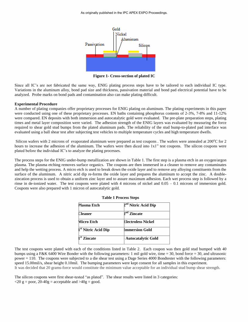
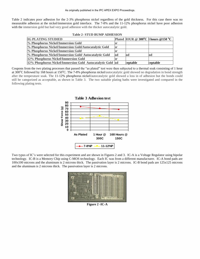
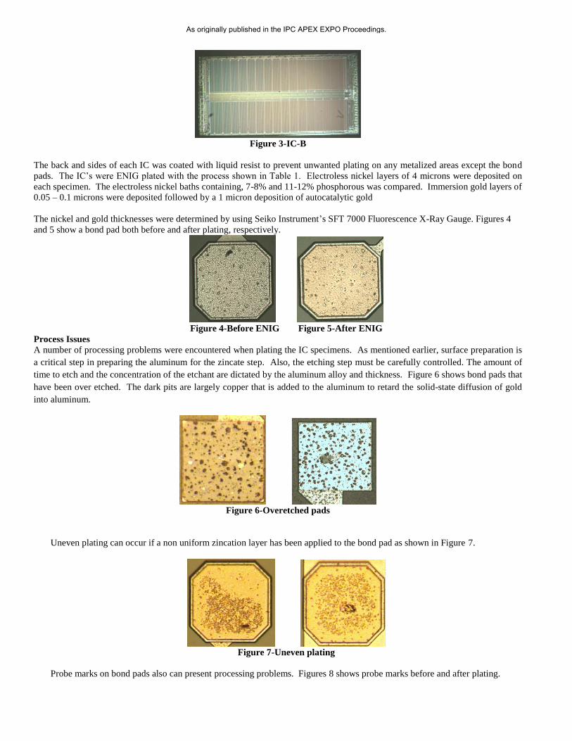
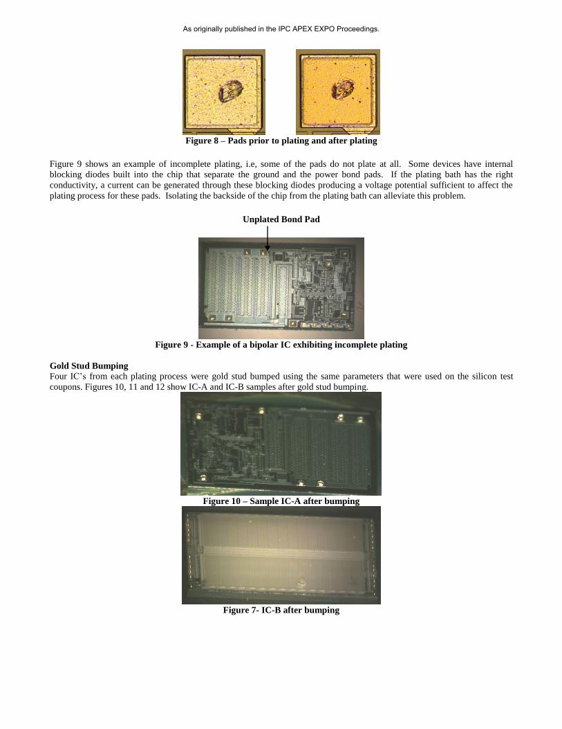
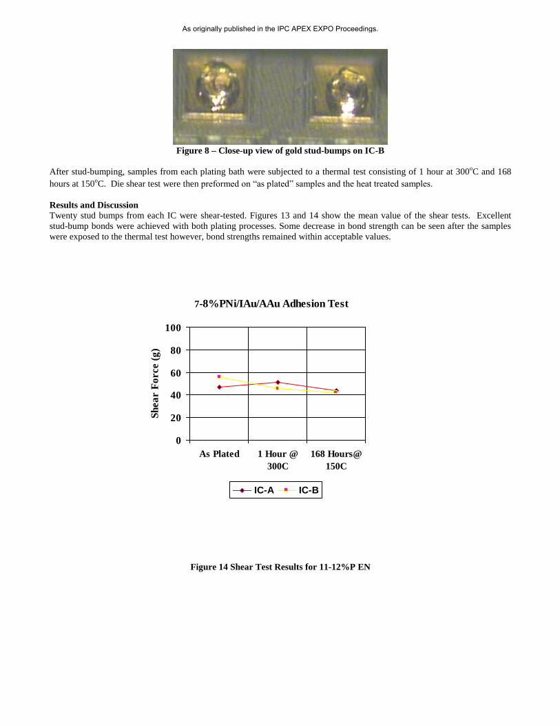
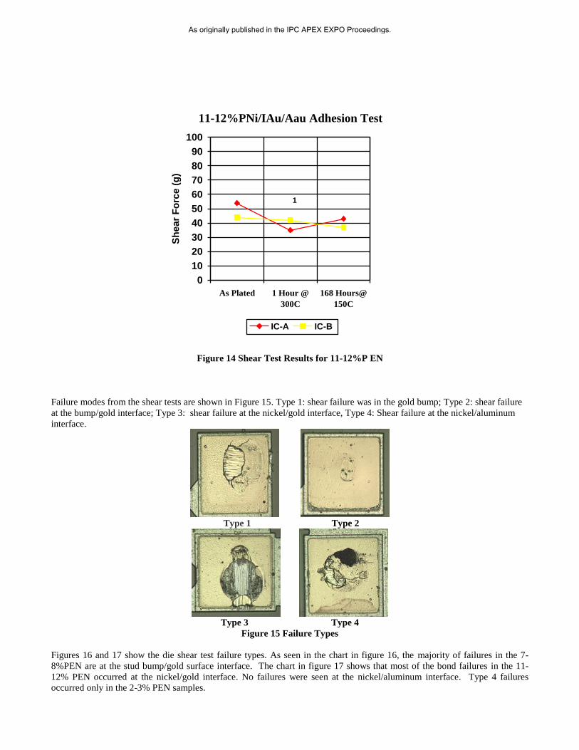
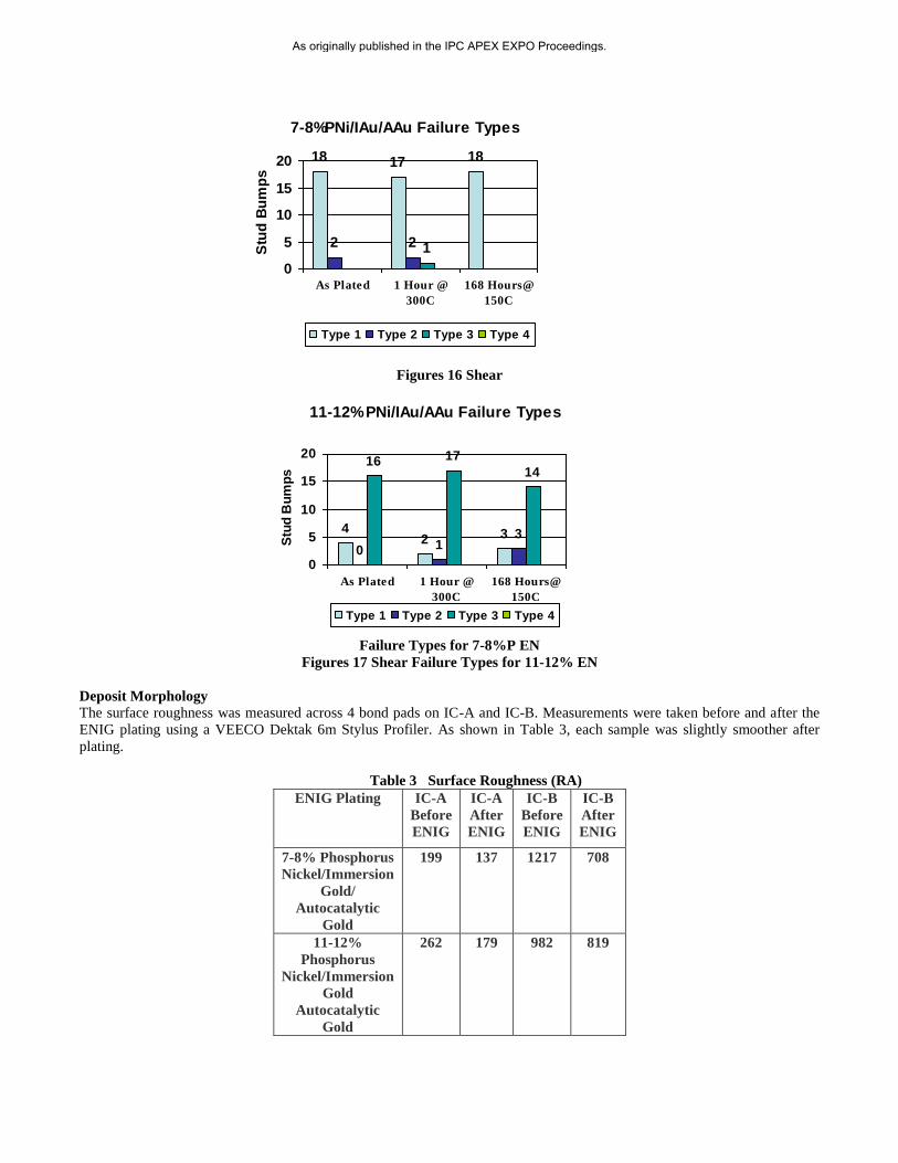
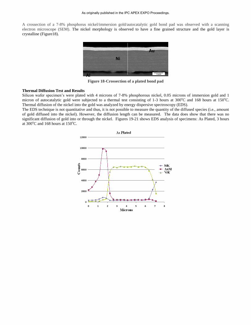
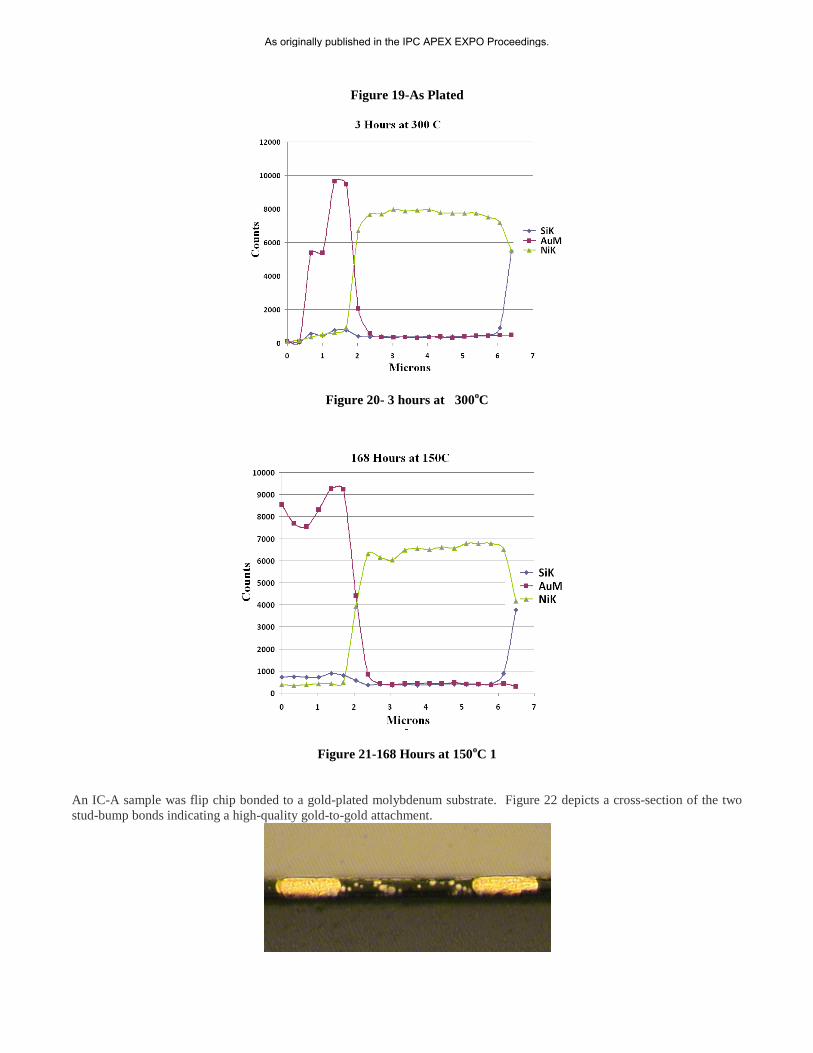
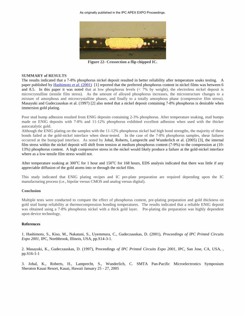