sagar report final.pdf
TRANSCRIPT

A
REPORT ON
45 DAYS SUMMER TRAINING PROGRAMME
TAKEN AT
BIRLA INSTITUTE OF SCIENTIFIC RESEARCH
JAIPUR
2012
BANSAL SCHOOL OF ENGINEERING AND TECHNOLOGY
JAIPUR
SUBMITTED TO SUBMITTED BY
DEPARTMENT OF ELECTRONICS Sagar Bhargava
BIRLA INSTITUTE OF SCIENTIFIC RESEARCH B.S.E.T
JAIPUR JAIPUR

CERTIFICATE
This is to certify that Mr. Sagar Bhargava (Electronics & Communication) has successfully completed his Summer Training during May-July 2012. The project was undertaken by him at Birla Institute of Scientific Research titled “8 bit ALU” & “Processor” using VHDL. The project on evaluation fulfills all the stated criteria and the student's findings are his original work. I hereby certify her work excellent to the best of my knowledge. Dated: 10.07.2012 Mr. P. S. Rathore Training In charge...
BISR- Jaipur.........

PREFACE
The concept of Industrial Training intends to increase the knowledge and skills of the student, to make him capable of doing a particular job efficiently. The purpose of training is to bring a gap between job requirement and job competence. Training is aimed at improving the behavior and performance of a person. During Training at Birla Institute of Scientific Research, Jaipur I got the knowledge of the essential elements required for the completion of electronic based projects. Hence I have made this report on the basis of knowledge I got during my Training period.

ACKNOWLEDGEMENT
I am highly indebted to the Director of Birla Institute of Scientific Research, Jaipur for allowing me to do my Summer Training as well as for his guidance and constant supervision. I am thankful to Prof. J. B. Gupta, Prof. P.S. Rathore (training in charge), Mrs. Jyoti Sharma, Mr. Jitendra Gupta & Mr. Uma Shankar for their kind and active support and valuable guidance during the training.
I have taken efforts in the project. However, it would not have been possible without the kind support and many individuals and organizations. I would like to extend my sincere thanks to each and every member related to Birla Institute of Scientific Research.
Place: Jaipur (SAGAR BHARGAVA)
Date: 10.07.2012 B.S.E.T.
Jaipur

Contents
1 INTRODUCTION TO VLSI DESIGN 4
1.1 INTRODUCTION . . . . . . . . . . . . . . . . . . . . . . . . . . 41.2 CONVENTIONAL APPROACH TO DIGITAL DESIGN . . . . 41.3 VLSI DESIGN . . . . . . . . . . . . . . . . . . . . . . . . . . . . 6
1.3.1 Abstraction Model . . . . . . . . . . . . . . . . . . . . . . 71.4 ASIC DESIGN FLOW . . . . . . . . . . . . . . . . . . . . . . . . 7
1.4.1 Design Description . . . . . . . . . . . . . . . . . . . . . . 91.4.2 Optimization . . . . . . . . . . . . . . . . . . . . . . . . . 91.4.3 Simulation . . . . . . . . . . . . . . . . . . . . . . . . . . 91.4.4 Synthesis . . . . . . . . . . . . . . . . . . . . . . . . . . . 111.4.5 Physical Design . . . . . . . . . . . . . . . . . . . . . . . . 111.4.6 Post Layout Simulation . . . . . . . . . . . . . . . . . . . 121.4.7 Critical Subsystems . . . . . . . . . . . . . . . . . . . . . 12
1.5 ROLE OF HDL . . . . . . . . . . . . . . . . . . . . . . . . . . . . 12
2 Architecture of FPGAs and CPLDs 13
2.1 Introduction to High-Capacity FPDs . . . . . . . . . . . . . . . . 132.1.1 De�nitions of Relevant Terminology . . . . . . . . . . . . 14
2.2 Evolution of Programmable Logic Devices . . . . . . . . . . . . . 152.3 User-Programmable Switch Technologies . . . . . . . . . . . . . . 172.4 Computer Aided Design (CAD) Flow for FPDs . . . . . . . . . . 192.5 Applications of CPLDs . . . . . . . . . . . . . . . . . . . . . . . . 21
3 VHDL 22
3.1 Introduction . . . . . . . . . . . . . . . . . . . . . . . . . . . . . . 223.2 A standard language . . . . . . . . . . . . . . . . . . . . . . . . . 233.3 Entities and Architectures . . . . . . . . . . . . . . . . . . . . . . 23
3.3.1 Entity declaration . . . . . . . . . . . . . . . . . . . . . . 233.3.2 Architecture declaration and body . . . . . . . . . . . . . 24
3.4 Design Units . . . . . . . . . . . . . . . . . . . . . . . . . . . . . 243.4.1 Entities . . . . . . . . . . . . . . . . . . . . . . . . . . . . 243.4.2 Architectures . . . . . . . . . . . . . . . . . . . . . . . . . 253.4.3 Packages and package bodies . . . . . . . . . . . . . . . . 253.4.4 Con�gurations . . . . . . . . . . . . . . . . . . . . . . . . 27
1

4 Projects 28
4.1 ALU 8 Bit . . . . . . . . . . . . . . . . . . . . . . . . . . . . . . . 284.1.1 *.vhd Code . . . . . . . . . . . . . . . . . . . . . . . . . . 284.1.2 Test Bench Code . . . . . . . . . . . . . . . . . . . . . . . 29
4.2 Processor . . . . . . . . . . . . . . . . . . . . . . . . . . . . . . . 304.2.1 *.vhd Code . . . . . . . . . . . . . . . . . . . . . . . . . . 304.2.2 Test Bench Code . . . . . . . . . . . . . . . . . . . . . . . 36
5 Xilinx ISE and Spartan-3 39
5.1 Introduction . . . . . . . . . . . . . . . . . . . . . . . . . . . . . . 395.1.1 Part 1: Starting a new Project . . . . . . . . . . . . . . . 395.1.2 Part 2: Generating a PROM File . . . . . . . . . . . . . . 48
2

List of Figures
1.1 A simple digital circuit. . . . . . . . . . . . . . . . . . . . . . . . 51.2 Sequence of steps in conventional electronic circuit design. . . . . 61.3 Design domain and levels of abstraction. . . . . . . . . . . . . . . 81.4 Major activities in ASIC design. . . . . . . . . . . . . . . . . . . 81.5 ASIC design and development �ow. . . . . . . . . . . . . . . . . . 10
2.1 Structure of a PAL. . . . . . . . . . . . . . . . . . . . . . . . . . 162.2 Structure of an FPGA. . . . . . . . . . . . . . . . . . . . . . . . . 182.3 FPD Categories by Logic Capacity. . . . . . . . . . . . . . . . . . 192.4 CAD Design Flow for SPLDs. . . . . . . . . . . . . . . . . . . . . 20
4.1 ALU Simulation in Xilinx ISE . . . . . . . . . . . . . . . . . . . . 304.2 Processor Simulation in Xilinx ISE . . . . . . . . . . . . . . . . . 38
5.1 Xilinx Window . . . . . . . . . . . . . . . . . . . . . . . . . . . . 405.2 New Project Window . . . . . . . . . . . . . . . . . . . . . . . . . 415.3 Project Source Properties Window . . . . . . . . . . . . . . . . . 425.4 Module Nomenclature Window . . . . . . . . . . . . . . . . . . . 435.5 Source De�ning Window . . . . . . . . . . . . . . . . . . . . . . . 445.6 Summary . . . . . . . . . . . . . . . . . . . . . . . . . . . . . . . 455.7 Project Navigator Window . . . . . . . . . . . . . . . . . . . . . 465.8 Code Window . . . . . . . . . . . . . . . . . . . . . . . . . . . . . 475.9 FPGA Pins De�nation . . . . . . . . . . . . . . . . . . . . . . . . 495.10 Prompt . . . . . . . . . . . . . . . . . . . . . . . . . . . . . . . . 495.11 Xilinx Pace . . . . . . . . . . . . . . . . . . . . . . . . . . . . . . 505.12 PROM Con�guration Files . . . . . . . . . . . . . . . . . . . . . 515.13 Prepare PROM Files . . . . . . . . . . . . . . . . . . . . . . . . . 525.14 Con�gure Xilinx PROM Device . . . . . . . . . . . . . . . . . . . 535.15 Summary Wizard . . . . . . . . . . . . . . . . . . . . . . . . . . . 545.16 Add Files . . . . . . . . . . . . . . . . . . . . . . . . . . . . . . . 555.17 Adding Source Bit Files . . . . . . . . . . . . . . . . . . . . . . . 565.18 Adding Device . . . . . . . . . . . . . . . . . . . . . . . . . . . . 575.19 PROM File Generation . . . . . . . . . . . . . . . . . . . . . . . 585.20 Final Output Window . . . . . . . . . . . . . . . . . . . . . . . . 585.21 Save Project . . . . . . . . . . . . . . . . . . . . . . . . . . . . . . 59
3
Chapter 1
INTRODUCTION TO VLSI
DESIGN
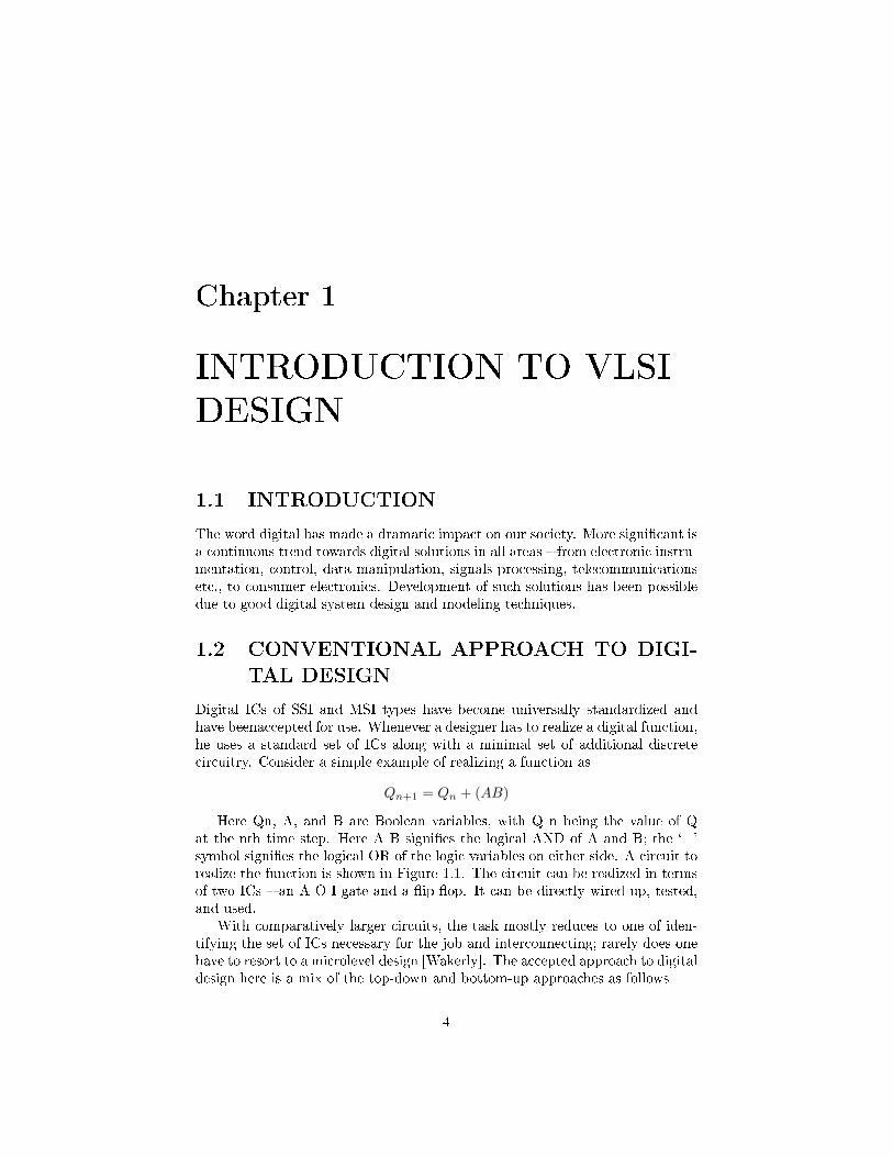
1.1 INTRODUCTION
The word digital has made a dramatic impact on our society. More signi�cant isa continuous trend towards digital solutions in all areas � from electronic instru-mentation, control, data manipulation, signals processing, telecommunicationsetc., to consumer electronics. Development of such solutions has been possibledue to good digital system design and modeling techniques.
1.2 CONVENTIONAL APPROACH TO DIGI-TAL DESIGN
Digital ICs of SSI and MSI types have become universally standardized andhave beenaccepted for use. Whenever a designer has to realize a digital function,he uses a standard set of ICs along with a minimal set of additional discretecircuitry. Consider a simple example of realizing a function as
Qn+1 = Qn + (AB)
Here Qn, A, and B are Boolean variables, with Q n being the value of Qat the nth time step. Here A B signi�es the logical AND of A and B; the `+'symbol signi�es the logical OR of the logic variables on either side. A circuit torealize the function is shown in Figure 1.1. The circuit can be realized in termsof two ICs � an A-O-I gate and a �ip-�op. It can be directly wired up, tested,and used.
With comparatively larger circuits, the task mostly reduces to one of iden-tifying the set of ICs necessary for the job and interconnecting; rarely does onehave to resort to a microlevel design [Wakerly]. The accepted approach to digitaldesign here is a mix of the top-down and bottom-up approaches as follows
4

Figure 1.1: A simple digital circuit.
� Decide the requirements at the system level and translate them to circuitrequirements.
� Identify the major functional blocks required like timer, DMA unit, reg-ister�le etc., say as in the design of a processor.
� Whenever a function can be realized using a standard IC, use the same�for example programmable counter, mux, demux, etc.
� Whenever the above is not possible, form the circuit to carry out the blockfunctions using standard SSI � for example gates, �ip-�ops, etc.
� Use additional components like transistor, diode, resistor, capacitor, etc.,wherever essential.
Once the above steps are gone through, a paper design is ready. Starting withthe paper design, one has to do a circuit layout. The physical location of allthe components is tentatively decided; they are interconnected and the `circuit-onpaper' is made ready. Once a paper design is done, a layout is carried outand a net-list prepared. Based on this, the PCB is fabricated, and populatedand all the populated cards tested and debugged. The procedure is shown as aprocess �owchart in Figure 1.2
At the debugging stage one may encounter three types of problems:
� Functional mismatch: The realized and expected functions are di�erent.One may have to go through the relevant functional block carefully andlocate any error logically. Finally the necessary correction has to be carriedout in hardware.
� Timing mismatch: The problem can manifest in di�erent forms. Onepossibility is due to the signal going through di�erent propagation delaysin two paths and arriving at a point with a timing mismatch. This cancause faulty operation. Another possibility is a race condition in a cir-cuit involving asynchronous feedback. This kind of problem may call forelaborate debugging. The preferred practice is to do debugging at smaller
5

Figure 1.2: Sequence of steps in conventional electronic circuit design.
module stages and ensuring that feedback through larger loops is avoided:It becomes essential to check for the existence of long asynchronous loops.
� Overload: Some signals may be overloaded to such an extent that thesignal transition may be unduly delayed or even suppressed. The problemmanifests as re�ections and erratic behavior in some cases (The signal hasto be suitably bu�ered here.). In fact, overload on a signal can lead totiming mismatches.
The above have to be carried out after completion of the prototype PCB man-ufacturing; it involves cost, time, and also a redesigning process to develop abugfree design.
1.3 VLSI DESIGN
The complexity of VLSIs being designed and used today makes the manualapproach to design impractical. Design automation is the order of the day.With the rapid technological developments in the last two decades, the statusof VLSI technology is characterized by the following [Wai-kai, Gopalan]: � Asteady increase in the size and hence the functionality of the ICs.
� A steady reduction in feature size and hence increase in the speed ofoperation as well as gate or transistor density.
6
� A steady improvement in the predictability of circuit behavior.
� A steady increase in the variety and size of software tools for VLSI design.
The above developments have resulted in a proliferation of approaches to VLSIdesign. We brie�y describe the procedure of automated design �ow [Rabaey,Smith MJ]. The aim is more to bring out the role of a Hardware DescriptionLanguage (HDL) in the design process. An abstraction based model is the basisof the automated design.
1.3.1 Abstraction Model
The model divides the whole design cycle into various domains (see Figure 1.3).With such an abstraction through a division process the design is carried outin di�erent layers. The designer at one layer can function without botheringabout the layers above or below. The thick horizontal lines separating thelayers in the �gure signify the compartmentalization. As an example, let usconsider design at the gate level. The circuit to be designed would be describedin terms of truth tables and state tables. With these as available inputs, he hasto express them as Boolean logic equations and realize them in terms of gatesand �ip-�ops. In turn, these form the inputs to the layer immediately below.Compartmentalization of the approach to design in the manner described hereis the essence of abstraction; it is the basis for development and use of CADtools in VLSI design at various levels.
The design methods at di�erent levels use the respective aids such as Booleanequations, truth tables, state transition table, etc. But the aids play only asmall role in the process. To complete a design, one may have to switch fromone tool to another, raising the issues of tool compatibility and learning newenvironments.
1.4 ASIC DESIGN FLOW
As with any other technical activity, development of an ASIC starts with anidea and takes tangible shape through the stages of development as shown inFigure 1.4 and shown in detail in Figure 1.5. The �rst step in the process is toexpand the idea in terms of behavior of the target circuit. Through stages ofprogramming, the same is fully developed into a design description � in termsof well de�ned standard constructs and conventions.
The design is tested through a simulation process; it is to check, verify,and ensure that what is wanted is what is described. Simulation is carried outthrough dedicated tools. With every simulation run, the simulation results arestudied to identify errors in the design description. The errors are corrected andanother simulation run carried out. Simulation and changes to design descrip-tion together form a cyclic iterative process, repeated until an error-free designis evolved.
7

Figure 1.3: Design domain and levels of abstraction.
Figure 1.4: Major activities in ASIC design.
8

Design description is an activity independent of the target technology ormanufacturer. It results in a description of the digital circuit. To translate itinto a tangible circuit, one goes through the physical design process. The sameconstitutes a set of activities closely linked to the manufacturer and the targettechnology.
1.4.1 Design Description
The design is carried out in stages. The process of transforming the idea intoa detailed circuit description in terms of the elementary circuit componentsconstitutes design description. The �nal circuit of such an IC can have up to abillion such components; it is arrived at in a step-by-step manner.
The �rst step in evolving the design description is to describe the circuitin terms of its behavior. The description looks like a program in a high levellanguage like C. Once the behavioral level design description is ready, it is testedextensively with the help of a simulation tool; it checks and con�rms that all theexpected functions are carried out satisfactorily. If necessary, this behaviorallevel routine is edited, modi�ed, and rerun � all done manually. Finally, onehas a design for the expected system � described at the behavioral level. Thebehavioral design forms the input to the synthesis tools, for circuit synthesis.The behavioral constructs not supported by the synthesis tools are replaced bydata �ow and gate level constructs. To surmise, the designer has to developsynthesizable codes for his design.
The design at the behavioral level is to be elaborated in terms of knownand acknowledged functional blocks. It forms the next detailed level of designdescription. Once again the design is to be tested through simulation and iter-atively corrected for errors. The elaboration can be continued one or two stepsfurther. It leads to a detailed design description in terms of logic gates andtransistor switches.
1.4.2 Optimization
The circuit at the gate level � in terms of the gates and �ip-�ops � can beredundant in nature. The same can be minimized with the help of minimizationtools. The step is not shown separately in the �gure. The minimized logicaldesign is converted to a circuit in terms of the switch level cells from standardlibraries provided by the foundries. The cell based design generated by the toolis the last step in the logical design process; it forms the input to the �rst levelof physical design [Micheli].
1.4.3 Simulation
The design descriptions are tested for their functionality at every level � behav-ioral, data �ow, and gate. One has to check here whether all the functions arecarried out as expected and rectify them. All such activities are carried out bythe simulation tool. The tool also has an editor to carry out any corrections
9
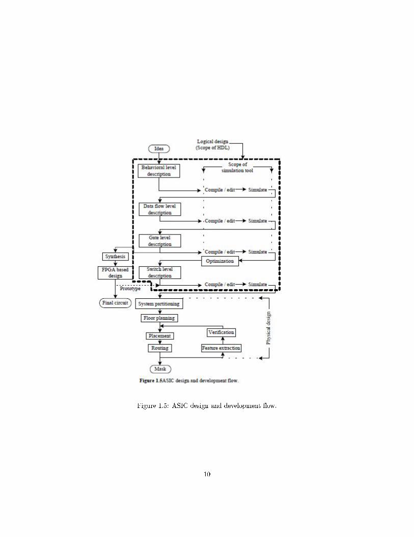
Figure 1.5: ASIC design and development �ow.
10

to the source code. Simulation involves testing the design for all its functions,functional sequences, timing constraints, and speci�cations. Normally testingand simulation at all the levels � behavioral to switch level � are carried out bya single tool; the same is identi�ed as �scope of simulation tool� in Figure 1.5.
1.4.4 Synthesis
With the availability of design at the gate (switch) level, the logical design iscomplete. The corresponding circuit hardware realization is carried out by asynthesis tool. Two common approaches are as follows:
� The circuit is realized through an FPGA [Old�eld]. The gate level designdescription is the starting point for the synthesis here. The FPGA vendorsprovide an interface to the synthesis tool. Through the interface the gatelevel design is realized as a �nal circuit. With many synthesis tools, onecan directly use the design description at the data �ow level itself to realizethe �nal circuit through an FPGA. The FPGA route is attractive forlimited volume production or a fast development cycle.
� The circuit is realized as an ASIC. A typical ASIC vendor will have his ownlibrary of basic components like elementary gates and �ip-�ops. Eventu-ally the circuit is to be realized by selecting such components and inter-connecting them conforming to the required design. This constitutes thephysical design. Being an elaborate and costly process, a physical designmay call for an intermediate functional veri�cation through the FPGAroute. The circuit realized through the FPGA is tested as a prototype.It provides another opportunity for testing the design closer to the �nalcircuit.
1.4.5 Physical Design
A fully tested and error-free design at the switch level can be the starting pointfor a physical design [Baker & Boyce, Wolf]. It is to be realized as the �nalcircuit using (typically) a million components in the foundry's library. Thestep-by-step activities in the process are described brie�y as follows:
� System partitioning: The design is partitioned into convenient compart-ments or functional blocks. Often it would have been done at an earlierstage itself and the software design prepared in terms of such blocks. In-terconnection of the blocks is part of the partition process.
� Floor planning: The positions of the partitioned blocks are planned andthe blocks are arranged accordingly. The procedure is analogous to theplanning and arrangement of domestic furniture in a residence. Blockswith I/O pins are kept close to the periphery; those which interact fre-quently or through a large number of interconnections are kept close to-gether, and so on. Partitioning and �oor planning may have to be carriedout and re�ned iteratively to yield best results.
11
� Placement: The selected components from the ASIC library are placed inposition on the �Silicon �oor.� It is done with each of the blocks above.
� Routing: The components placed as described above are to be intercon-nected to the rest of the block: It is done with each of the blocks by suit-ably routing the interconnects. Once the routing is complete, the physicaldesign cam is taken as complete. The �nal mask for the design can bemade at this stage and the ASIC manufactured in the foundry.
1.4.6 Post Layout Simulation
Once the placement and routing are completed, the performance speci�cationslike silicon area, power consumed, path delays, etc., can be computed. Equiva-lent circuit can be extracted at the component level and performance analysiscarried out. This constitutes the �nal stage called �veri�cation.� One may haveto go through the placement and routing activity once again to improve perfor-mance.
1.4.7 Critical Subsystems
The design may have critical subsystems. Their performance may be crucialto the overall performance; in other words, to improve the system performancesubstantially, one may have to design such subsystems afresh. The design heremay imply rede�nition of the basic feature size of the component, componentdesign, placement of components, or routing done separately and speci�cally forthe subsystem. A set of masks used in the foundry may have to be done afreshfor the purpose.
1.5 ROLE OF HDL
An HDL provides the framework for the complete logical design of the ASIC.All the activities coming under the purview of an HDL are shown enclosed inbold dotted lines in Figure 1.4. Verilog and VHDL are the two most commonlyused HDLs today. Both have constructs with which the design can be fullydescribed at all the levels. There are additional constructs available to facilitatesetting up of the test bench, spelling out test vectors for them and �observing�the outputs from the designed unit.
IEEE has brought out Standards for the HDLs, and the software tools con-form to them. Verilog as an HDL was introduced by Cadence Design Systems;they placed it into the public domain in 1990. It was established as a formalIEEE Standard in 1995. The revised version has been brought out in 2001.However, most of the simulation tools available today conform only to the 1995version of the standard.
12
Chapter 2
Architecture of FPGAs and
CPLDs
2.1 Introduction to High-Capacity FPDs
Prompted by the development of new types of sophisticated �eld-programmabledevices (FPDs), the process of designing digital hardware has changed dramati-cally over the past few years. Unlike previous generations of technology, in whichboard-level designs included large numbers of SSI chips containing basic gates,virtually every digital design produced today consists mostly of high-densitydevices. This applies not only to custom devices like processors and memory,but also for logic circuits such as state machine controllers, counters, registers,and decoders. When such circuits are destined for high-volume systems theyhave been integrated into high-density gate arrays. However, gate array NREcosts often are too expensive and gate arrays take too long to manufacture to beviable for prototyping or other low-volume scenarios. For these reasons, mostprototypes, and also many production designs are now built using FPDs. Themost compelling advantages of FPDs are instant manufacturing turnaround,low start-up costs, low �nancial risk and (since programming is done by the enduser) ease of design changes.
The market for FPDs has grown dramatically over the past decade to thepoint where there is now a wide assortment of devices to choose from. A designertoday faces a daunting task to research the di�erent types of chips, understandwhat they can best be used for, choose a particular manufacturers's product,learn the intricacies of vendor-speci�c software and then design the hardware.Confusion for designers is exacerbated by not only the sheer number of FPDsavailable, but also by the complexity of the more sophisticated devices. Thepurpose of this paper is to provide an overview of the architecture of the varioustypes of FPDs. The emphasis is on devices with relatively high logic capacity;all of the most important commercial products are discussed.
Before proceeding, we provide de�nitions of the terminology in this �eld.
13

This is necessary because the technical jargon has become somewhat inconsistentover the past few years as companies have attempted to compare and contrasttheir products in literature.
2.1.1 De�nitions of Relevant Terminology
The most important terminology used in this report are de�ned below:
� Field-Programmable Device (FPD) � a general term that refers to anytype of integrated circuit used for implementing digital hardware, wherethe chip can be con�gured by the end user to realize di�erent designs.Programming of such a device often involves placing the chip into a specialprogramming unit, but some chips can also be con�gured �in-system�.Another name for FPDs is programmable logic devices (PLDs); althoughPLDs encompass the same types of chips as FPDs, we prefer the termFPD because historically the word PLD has referred to relatively simpletypes of devices.
� PLA� a Programmable Logic Array (PLA) is a relatively small FPD thatcontains two levels of logic, an AND-plane and an OR-plane, where bothlevels are programmable (note: although PLA structures are sometimesembedded into full-custom chips, we refer here only to those PLAs thatare provided as separate integrated circuits and are user-programmable).
� CPLD� amore Complex PLD that consists of an arrangement of multipleSPLD-like blocks on a single chip. Alternative names (that will not beused in this paper) sometimes adopted for this style of chip are EnhancedPLD (EPLD), Super PAL, Mega PAL, and others.
� FPGA� a Field-Programmable Gate Array is an FPD featuring a generalstructure that allows very high logic capacity. Whereas CPLDs featurelogic resources with a wide number of inputs (AND planes), FPGAs o�ermore narrow logic resources. FPGAs also o�er a higher ratio of �ip-�opsto logic resources than do CPLDs.
� HCPLDs � high-capacity PLDs: a single acronym that refers to bothCPLDs and FPGAs. This term has been coined in trade literature forproviding an easy way to refer to both types of devices.
� Interconnect � the wiring resources in an FPD.
� Programmable Switch � a user-programmable switch that can connect alogic element to an interconnect wire, or one interconnect wire to another.
� Logic Block � a relatively small circuit block that is replicated in anarray in an FPD. When a circuit is implemented in an FPD, it is �rstdecomposed into smaller sub-circuits that can each be mapped into a logicblock. The term logic block is mostly used in the context of FPGAs, butit could also refer to a block of circuitry in a CPLD.
14

� Logic Capacity � the amount of digital logic that can be mapped intoa single FPD. This is usually measured in units of �equivalent numberof gates in a traditional gate array�. In other words, the capacity of anFPD is measured by the size of gate array that it is comparable to. Insimpler terms, logic capacity can be thought of as �number of 2-inputNAND gates�.
� Logic Density�the amount of logic per unit area in an FPD.
� Speed-Performance � measures the maximum operable speed of a circuitwhen implemented in an FPD. For combinational circuits, it is set bythe longest delay through any path, and for sequential circuits it is themaximum clock frequency for which the circuit functions properly.
In the remainder of this section, to provide insight into FPD development theevolution of FPDs over the past two decades is described. Additional back-ground information is also included on the semiconductor technologies used inthe manufacture of FPDs.
2.2 Evolution of Programmable Logic Devices
The �rst type of user-programmable chip that could implement logic circuitswas the Programmable Read-Only Memory (PROM), in which address linescan be used as logic circuit inputs and data lines as outputs. Logic functions,however, rarely require more than a few product terms, and a PROM containsa full decoder for its address inputs. PROMS are thus an ine�cient architecturefor realizing logic circuits, and so are rarely used in practice for that purpose.The �rst device developed later speci�cally for implementing logic circuits wasthe Field-Programmable Logic Array (FPLA), or simply PLA for short. APLA consists of two levels of logic gates: a programmable �wired� AND-planefollowed by a programmable �wired� OR-plane. A PLA is structured so that anyof its inputs (or their complements) can be AND'ed together in the AND-plane;each AND-plane output can thus correspond to any product term of the inputs.Similarly, each ORplane output can be con�gured to produce the logical sumof any of the AND-plane outputs. With this structure, PLAs are well-suitedfor implementing logic functions in sum-of-products form. They are also quiteversatile, since both the AND terms and OR terms can have many inputs (thisfeature is often referred to as wide AND and OR gates).
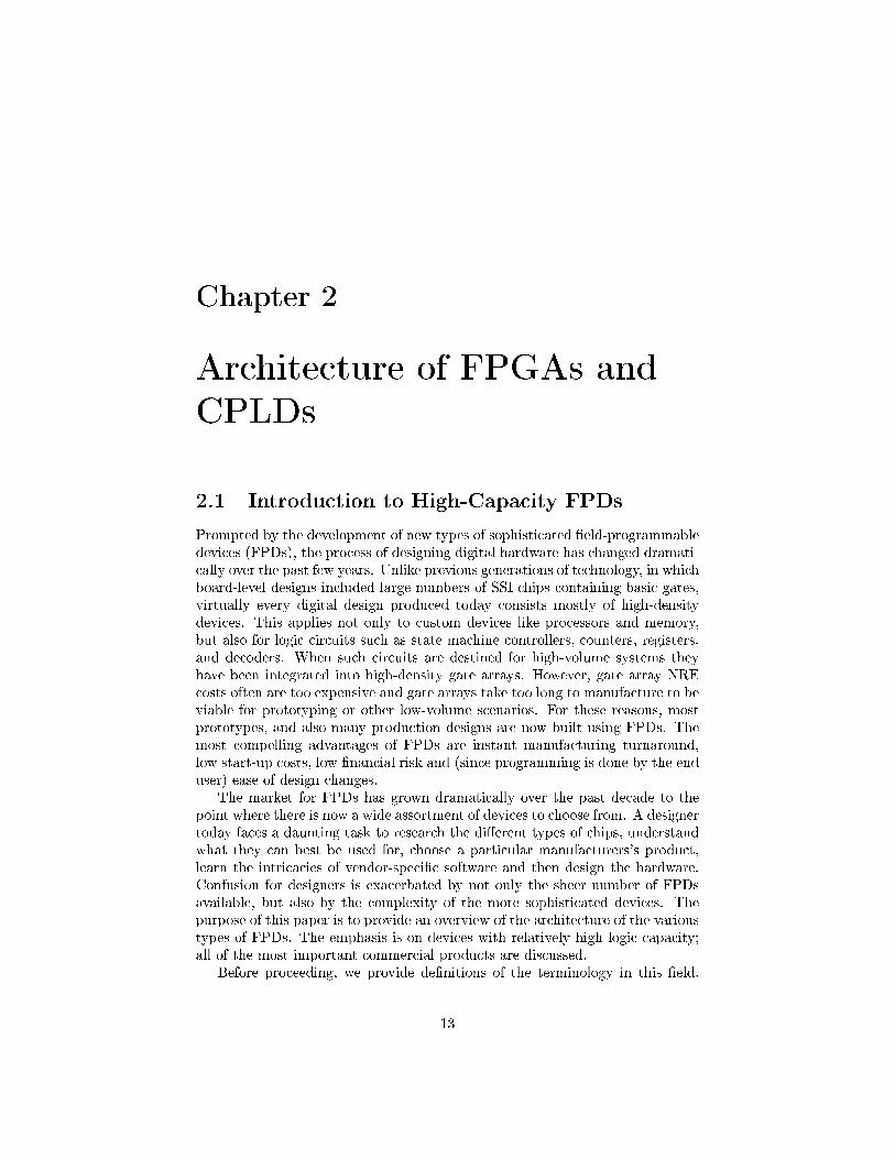
When PLAs were introduced in the early 1970s, by Philips, their main draw-backs were that they were expensive to manufacture and o�ered somewhat poorspeed-performance. Both disadvantages were due to the two levels of con�g-urable logic, because programmable logic planes were di�cult to manufactureand introduced signi�cant propagation delays. To overcome these weaknesses,Programmable Array Logic (PAL) devices were developed. As Figure 1 illus-trates, PALs feature only a single level of programmability, consisting of a pro-grammable �wired� ANDplane that feeds �xed OR-gates. To compensate for
15
Figure 2.1: Structure of a PAL.
lack of generality incurred because the OR-plane is �xed, several variants ofPALs are produced, with di�erent numbers of inputs and outputs, and varioussizes of OR-gates. PALs usually contain �ip-�ops connected to the OR-gateoutputs so that sequential circuits can be realized. PAL devices are importantbecause when introduced they had a profound e�ect on digital hardware design,and also they are the basis for some of the newer, more sophisticated archi-tectures that will be described shortly. Variants of the basic PAL architectureare featured in several other products known by di�erent acronyms. All smallPLDs, including PLAs, PALs, and PAL-like devices are grouped into a singlecategory called Simple PLDs (SPLDs), whose most important characteristicsare low cost and very high pin-to-pin speed-performance.
As technology has advanced, it has become possible to produce devices withhigher capacity than SPLDs. The di�culty with increasing capacity of a strictSPLD architecture is that the structure of the programmable logic-planes growtoo quickly in size as the number of inputs is increased. The only feasible way toprovide large capacity devices based on SPLD architectures is then to integratemultiple SPLDs onto a single chip and provide interconnect to programmablyconnect the SPLD blocks together. Many commercial FPD products exist onthe market today with this basic structure, and are collectively referred to asComplex PLDs (CPLDs).
CPLDs were pioneered by Altera, �rst in their family of chips called ClassicEPLDs, and then in three additional series, called MAX 5000, MAX 7000 and
16
MAX 9000. Because of a rapidly growing market for large FPDs, other manufac-turers developed devices in the CPLD category and there are now many choicesavailable. All of the most important commercial products will be describedin Section 2. CPLDs provide logic capacity up to the equivalent of about 50typical SPLD devices, but it is somewhat di�cult to extend these architecturesto higher densities. To build FPDs with very high logic capacity, a di�erentapproach is needed.
The highest capacity general purpose logic chips available today are the tra-ditional gate arrays sometimes referred to as Mask-Programmable Gate Arrays(MPGAs). MPGAs consist of an array of pre-fabricated transistors that canbe customized into the user's logic circuit by connecting the transistors withcustom wires. Customization is performed during chip fabrication by specifyingthe metal interconnect, and this means that in order for a user to employ anMPGA a large setup cost is involved and manufacturing time is long. AlthoughMPGAs are clearly not FPDs, they are mentioned here because they motivatedthe design of the user-programmable equivalent: Field- Programmable Gate Ar-rays (FPGAs). Like MPGAs, FPGAs comprise an array of uncommitted circuitelements, called logic blocks, and interconnect resources, but FPGA con�gura-tion is performed through programming by the end user. An illustration of atypical FPGA architecture appears in Figure 2.2. As the only type of FPD thatsupports very high logic capacity, FPGAs have been responsible for a majorshift in the way digital circuits are designed.
Figure 2.3 summarizes the categories of FPDs by listing the logic capacitiesavailable in each of the three categories. In the �gure, �equivalent gates� refersloosely to �number of 2-input NAND gates�. The chart serves as a guide for se-lecting a speci�c device for a given application, depending on the logic capacityneeded. However, as we will discuss shortly, each type of FPD is inherently bet-ter suited for some applications than for others. It should also be mentioned thatthere exist other special-purpose devices optimized for speci�c applications (e.g.state machines, analog gate arrays, large interconnection problems). However,since use of such devices is limited they will not be described here. The nextsub-section discusses the methods used to implement the user-programmableswitches that are the key to the user-customization of FPDs.
2.3 User-Programmable Switch Technologies
The �rst type of user-programmable switch developed was the fuse used in PLAs.Although fuses are still used in some smaller devices, we will not discuss themhere because they are quickly being replaced by newer technology. For higherdensity devices, where CMOS dominates the IC industry, di�erent approachesto implementing programmable switches have been developed. For CPLDs themain switch technologies (in commercial products) are �oating gate transistorslike those used in EPROM and EEPROM, and for FPGAs they are SRAM andantifuse. Each of these is brie�y discussed below.
An EEPROM or EPROM transistor is used as a programmable switch for
17
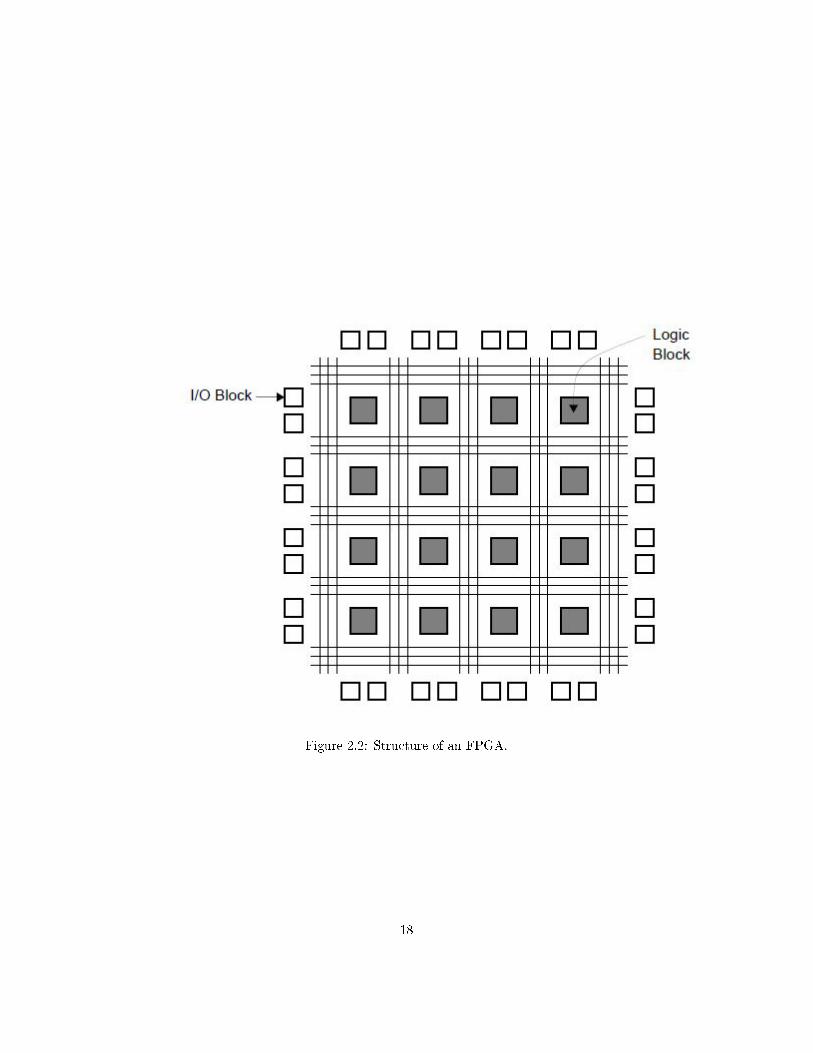
Figure 2.2: Structure of an FPGA.
18

Figure 2.3: FPD Categories by Logic Capacity.
CPLDs (and also for many SPLDs) by placing the transistor between two wiresin a way that facilitates implementation of wired-AND functions. This is illus-trated in Figure 4, which shows EPROM transistors as they might be connectedin an AND-plane of a CPLD. An input to the AND-plane can drive a productwire to logic level `0' through an EPROM transistor, if that input is part ofthe corresponding product term. For inputs that are not involved for a productterm, the appropriate EPROM transistors are programmed to be permanentlyturned o�. A diagram for an EEPROMbased device would look similar.
2.4 Computer Aided Design (CAD) Flow for FPDs
When designing circuits for implementation in FPDs, it is essential to employComputer-Aided Design (CAD) programs. Such software tools are discussedbrie�y in this section to provide a feel for the design process involved.
CAD tools are important not only for complex devices like CPLDs andFPGAs, but also for SPLDs. A typical CAD system for SPLDs would includesoftware for the following tasks: initial design entry, logic optimization, device�tting, simulation, and con�guration. This design �ow is illustrated in Figure2.4, which also indicates how some stages feed back to others. Design entrymay be done either by creating a schematic diagram with a graphical CADtool, by using a textbased system to describe a design in a simple hardware
19

Figure 2.4: CAD Design Flow for SPLDs.
description language, or with a mixture of design entry methods. Since initiallogic entry is not usually in an optimized form, algorithms are employed tooptimize the circuits, after which additional algorithms analyse the resultinglogic equations and ��t� them into the SPLD. Simulation is used to verify correctoperation, and the user would return to the design entry step to �x errors. Whena design simulates correctly it can be loaded into a programming unit and usedto con�gure an SPLD. One �nal detail to note about Figure 2.4 is that whilethe original design entry step is performed manually by the designer, all othersteps are carried out automatically by most CAD systems.
The steps involved for implementing circuits in CPLDs are similar to thosefor SPLDs, but the tools themselves are more sophisticated. Because the devicesare complex and can accommodate large designs, it is more common to use amixture of design entry methods for di�erent modules of a complete circuit. Forinstance, some modules might be designed with a small hardware descriptionlanguage like ABEL, others drawn using a symbolic schematic capture tool,and still others described via a full-featured hardware description language suchas VHDL. Also, for CPLDs the process of ��tting� a design may require stepssimilar to those described below for FPGAs, depending on how sophisticatedthe CPLD is. The necessary software for these tasks is supplied either by theCPLD manufacturer or a third party.
The design process for FPGAs is similar to that for CPLDs, but additionaltools are needed to support the increased complexity of the chips. The ma-jor di�erence is in the �device �tter� step that comes after logic optimizationand before simulation, where FPGAs require at least three steps: a technologymapper to map from basic logic gates into the FPGA's logic blocks, placementto choose which speci�c logic blocks to use in the FPGA, and a router to al-locate the wire segments in the FPGA to interconnect the logic blocks. Withthis added complexity, the CAD tools might require a fairly long period of time
20

(often more than an hour or even several hours) to complete their tasks.
2.5 Applications of CPLDs
We will now brie�y examine the types of applications which best suit CPLDarchitectures. Because they o�er high speeds and a range of capacities, CPLDsare useful for a very wide assortment of applications, from implementing randomglue logic to prototyping small gate arrays. One of the most common uses inindustry at this time, and a strong reason for the large growth of the CPLDmarket, is the conversion of designs that consist of multiple SPLDs into a smallernumber of CPLDs.
CPLDs can realize reasonably complex designs, such as graphics controller,LAN controllers, UARTs, cache control, and many others. As a general rule-of-thumb, circuits that can exploit wide AND/OR gates, and do not need a verylarge number of �ip-�ops are good candidates for implementation in CPLDs.A signi�cant advantage of CPLDs is that they provide simple design changesthrough re-programming (all commercial CPLD products are re-programmable).With insystem programmable CPLDs it is even possible to re-con�gure hardware(an example might be to change a protocol for a communications circuit) withoutpower-down.
Designs often partition naturally into the SPLD-like blocks in a CPLD. Theresult is more predictable speed-performance than would be the case if a designwere split into many small pieces and then those pieces were mapped into dif-ferent areas of the chip. Predictability of circuit implementation is one of thestrongest advantages of CPLD architectures.
21

Chapter 3
VHDL
3.1 Introduction
VHDL is a programming language that has been designed and optimized fordescribing the behavior of digital systems.
VHDL has many features appropriate for describing the behavior of elec-tronic components ranging from simple logic gates to complete microprocessorsand custom chips. Features of VHDL allow electrical aspects of circuit behav-ior (such as rise and fall times of signals, delays through gates, and functionaloperation) to be precisely described. The resulting VHDL simulation modelscan then be used as building blocks in larger circuits (using schematics, blockdiagrams or system-level VHDL descriptions) for the purpose of simulation.
VHDL is also a general-purpose programming language: just as high-levelprogramming languages allow complex design concepts to be expressed as com-puter programs, VHDL allows the behavior of complex electronic circuits tobe captured into a design system for automatic circuit synthesis or for systemsimulation. Like Pascal, C and C++, VHDL includes features useful for struc-tured design techniques, and o�ers a rich set of control and data representationfeatures. Unlike these other programming languages, VHDL provides featuresallowing concurrent events to be described. This is important because the hard-ware described using VHDL is inherently concurrent in its operation.
One of the most important applications of VHDL is to capture the perfor-mance speci�cation for a circuit, in the form of what is commonly referred to asa test bench. Test benches are VHDL descriptions of circuit stimuli and corre-sponding expected outputs that verify the behavior of a circuit over time. Testbenches should be an integral part of any VHDL project and should be createdin tandem with other descriptions of the circuit.
22
3.2 A standard language
One of the most compelling reasons for you to become experienced with andknowledgeable in VHDL is its adoption as a standard in the electronic designcommunity. Using a standard language such as VHDL virtually guarantees thatyou will not have to throw away and recapture design concepts simply becausethe design entry method you have chosen is not supported in a newer generationof design tools. Using a standard language also means that you are more likelyto be able to take advantage of the most up-to-date design tools and that youwill have access to a knowledge base of thousands of other engineers, many ofwhom are solving problems similar to your own.
3.3 Entities and Architectures
Every VHDL design description consists of at least one entity/architecture pair.(In VHDL jargon, this combination of an entity and its corresponding architec-ture is sometimes referred to as a design entity.) In a large design, you will typi-cally write many entity/architecture pairs and connect them together to form acomplete circuit. An entity declaration describes the circuit as it appears fromthe �outside� - from the perspective of its input and output interfaces. If youare familiar with schematics, you might think of the entity declaration as beinganalogous to a block symbol on a schematic. The second part of a minimalVHDL design description is the architecture declaration. Before simulation orsynthesis can proceed, every referenced entity in a VHDL design descriptionmust be bound with a corresponding architecture. The architecture describesthe actual function � or contents � of the entity to which it is bound. Usingthe schematic as a metaphor, you can think of the architecture as being roughlyanalogous to a lower-level schematic referenced by the higher-level functionalblock symbol.
3.3.1 Entity declaration
An entity declaration provides the complete interface for a circuit. Using theinformation provided in an entity declaration (the names, data types and di-rection of each port), you have all the information you need to connect thatportion of a circuit into other, higher-level circuits, or to develop input stimuli(in the form of a test bench) for veri�cation purposes. The actual operation ofthe circuit, however, is not included in the entity declaration.
Let's take a closer look at the entity declaration for this simple design de-scription:
�entity compare isport( A, B: in bit_vector(0 to 7);EQ: out bit);end compare;�
23

The entity declaration includes a name, compare, and a port statementde�ning all the inputs and outputs of the entity. The port list includes de�nitionsof three ports: A, B, and EQ. Each of these three ports is given a direction(either in, out or inout), and a type (in this case either bit_vector(0 to 7),which speci�es an 8-bit array, or bit, which represents a single-bit value).
There are many di�erent data types available in VHDL. To simplify thingsin this introductory circuit, we're going to stick with the simplest data types inVHDL, which are bit and bit_vector.
3.3.2 Architecture declaration and body
The second part of a minimal VHDL source �le is the architecture declaration.Every entity declaration you reference in your design must be accompanied byat least one corresponding architecture (we'll discuss why you might have morethan one architecture in a moment).
Here's the architecture declaration for the comparator circuit:�architecture compare1 of compare isbeginEQ <= '1' when (A = B) else '0';end compare1;�The architecture declaration begins with a unique name, compare1, followed
by the name of the entity to which the architecture is bound, in this case com-pare. Within the architecture declaration (between the begin and end keywords)is found the actual functional description of the comparator. There are manyways to describe combinational logic functions in VHDL; the method used inthis simple design description is a type of concurrent statement known as aconditional assignment. This assignment speci�es that the value of the output(EQ) will be assigned a value of '1' when A and B are equal, and a value of '0'when they di�er.
3.4 Design Units
One concept unique to VHDL (when compared to software programming lan-guages and to its main rival, Verilog) is the concept of a design unit. Designunits in VHDL (which may also be referred to as library units) are segments ofVHDL code that can be compiled separately and stored in a library.
There are actually �ve types of design units in VHDL; entities, architectures,packages, package bodies, and con�gurations. Entities and architectures are theonly two design units that you must have in any VHDL design description.Packages and con�gurations are optional.
3.4.1 Entities
A VHDL entity is a statement (indicated by the entity keyword) that de�nes theexternal speci�cation of a circuit or sub-circuit. The minimum VHDL design
24
description must include at least one entity and one corresponding architecture.When you write an entity declaration, you must provide a unique name for
that entity and a port list de�ning the input and output ports of the circuit.Each port in the port list must be given a name, direction (or mode, in VHDLjargon) and a type. Optionally, you may also include a special type of parameterlist (called a generic list) that allows you to pass additional information into anentity.
An example of an entity declaration is given below:entity fulladder is�port (X: in bit; Y: in bit;Cin: in bit;Cout: out bit;Sum: out bit);end fulladder;�
3.4.2 Architectures
A VHDL architecture declaration is a statement (beginning with the archi-tecture keyword) that describes the underlying function and/or structure of acircuit. Each architecture in your design must be associated (or bound) by namewith one entity in the design.
VHDL allows you to create more than one alternate architecture for eachentity. This feature is particularly useful for simulation and for project teamenvironments in which the design of the system interfaces (expressed as entities)is performed by a di�erent engineer than the lower-level architectural descriptionof each component circuit, or when you simply want to experiment with di�erentmethods of description.
An architecture declaration consists of zero or more declarations (of itemssuch as intermediate signals, components that will be referenced in the architec-ture, local functions and procedures, and constants) followed by a begin state-ment, a series of concurrent statements, and an end statement, as illustrated bythe following example:
architecture concurrent of fulladder isbeginSum <= X xor Y xor Cin;Cout <= (X and Y) or (X and Cin) or (Y and Cin);end concurrent;
3.4.3 Packages and package bodies
A VHDL package declaration is identi�ed by the package keyword, and is usedto collect commonlyused declarations for use globally among di�erent designunits. You can think of a package as a common storage area, one used to storesuch things as type declarations, constants, and global subprograms. Itemsde�ned within a package can be made visible to any other design unit in thecomplete VHDL design, and they can be compiled into libraries for later re-use.
25

A package can consist of two basic parts: a package declaration and anoptional package body. Package declarations can contain the following types ofstatements:
� Type and subtype declarations
� Constant declarations
� Global signal declarations
� Function and procedure declarations
� Attribute speci�cations
� File declarations
� Component declarations
� Alias declarations
� Disconnect speci�cations
� Use clauses
Items appearing within a package declaration can be made visible to other designunits through the use of a use statement.
If the package contains declarations of subprograms (functions or proce-dures) or de�nes one or more deferred constants (constants whose value is notimmediately given), then a package body is required in addition to the packagedeclaration. A package body (which is speci�ed using the package body keywordcombination) must have the same name as its corresponding package declara-tion, but it can be located anywhere in the design, in the same or a di�erentsource �le.
An example of a package is given below:�package conversion isfunction to_vector (size: integer; num: integer) returnstd_logic_vector;end conversion;package body conversion isfunction to_vector(size: integer; num: integer) return std_logic_vector isvariable ret: std_logic_vector (1 to size);variable a: integer;begina := num;for i in size downto 1 loopif ((a mod 2) = 1) thenret(i) := '1';else ret(i) := '0';end if;a := a / 2;
26

end loop;return ret;end to_vector;end conversion;
3.4.4 Con�gurations
The �nal type of design unit available in VHDL is called a con�guration decla-ration. You can think of a con�guration declaration as being roughly analogousto a parts list for your design. A con�guration declaration (identi�ed with thecon�guration keyword) speci�es which architectures are to be bound to whichentities, and it allows you to change how components are connected in yourdesign description at the time of simulation. (Con�gurations are not generallyused for synthesis, and may not be supported in the synthesis tool that you willuse.)
Con�guration declarations are always optional, no matter how complex adesign description you create. In the absence of a con�guration declaration,the VHDL standard speci�es a set of rules that provide you with a defaultcon�guration. For example, in the case where you have provided more than onearchitecture for an entity, the last architecture compiled will take precedenceand will be bound to the entity.
A simple example of a con�guration is given below:con�guration this_build of rcomp isfor structurefor COMP1: compare use entity work.compare(compare1);for ROT1: rotate use entity work.rotate(rotate1);end for;end this_build;
27

Chapter 4
Projects
4.1 ALU 8 Bit
4.1.1 *.vhd Code
library IEEE;use IEEE.STD_LOGIC_1164.ALL;use ieee.std_logic_unsigned.all;use ieee.std_logic_arith.all;use IEEE.NUMERIC_STD.ALL;library UNISIM; use UNISIM.VComponents.all;entity sagALU isport( a, b : in std_logic_vector(7 downto 0);op : in std_logic_vector(2 downto 0);zero : out std_logic; f : out std_logic_vector(7 downto 0));end sagALU;architecture Behavioral of sagALU isbeginprocess(op,a,b)variable nf: std_logic_vector(7 downto 0);begincase op is when "000" =>nf := a and b;when "100" =>nf := a or b;when "001" =>nf := a xor b;when "101" =>nf := a xnor b;when "010" =>nf := a + b;when "110" =>
28

nf := a - b;when "111" =>if a < b thennf := "11111111";end if;when others =>nf := "00000000";end case;if nf="00000000" thenzero <= '1';elsezero <= '0';end if;f <= nf;end process;end Behavioral;
4.1.2 Test Bench Code
LIBRARY ieee;USE ieee.std_logic_1164.ALL;ENTITY sagalutb ISEND sagalutb;ARCHITECTURE behavior OF sagalutb ISCOMPONENT sagALUPORT( a : IN std_logic_vector(7 downto 0);b : IN std_logic_vector(7 downto 0);op : IN std_logic_vector(2 downto 0);zero : OUT std_logic;f : OUT std_logic_vector(7 downto 0) );END COMPONENT;�Inputssignal a : std_logic_vector(7 downto 0) := (others => '0');signal b : std_logic_vector(7 downto 0) := (others => '0');signal op : std_logic_vector(2 downto 0) := (others => '0');�Outputssignal zero : std_logic; signal f : std_logic_vector(7 downto 0);BEGIN� Instantiate the Unit Under Test (UUT)uut: sagALU PORT MAP (a => a,b => b,op => op,zero => zero,f => f );� Stimulus process
29

Figure 4.1: ALU Simulation in Xilinx ISE
stim_proc: processbegin� hold reset state for 100 ns.wait for 100 ns;� insert stimulus herewait;end process;END;
4.2 Processor
4.2.1 *.vhd Code
�- CPU is a four register, 8 bit data/instruction, load/store machine.LIBRARY ieee;USE ieee.std_logic_1164.all; �- standard logicUSE ieee.std_logic_unsigned.all; �- arithmetic stu�ENTITY sagproc2 ISPORT( clk: IN std_logic; �- 50% duty cycle clockrd: inout std_logic; �- mem read cntlwr: inout std_logic; �- mem write cntl
30

addr: inout std_logic_vector(15 downto 0);�- the address busdata: INOUT std_logic_vector(7 downto 0); �- the data bussevseg: OUT std_logic_vector(6 downto 0); �- segven segment displaydin : IN std_logic_vector(15 DOWNTO 0); �- shell data indout : OUT std_logic_vector(7 DOWNTO 0); �- shell data outdsel : IN std_logic_vector(1 DOWNTO 0) �- shell data out select );END sagproc2;ARCHITECTURE one OF sagproc2 IS�- reset signal SIGNALreset: std_logic;�- cpu stateSIGNAL fetch, exec: std_logic;�-opcodesSIGNAL ld, st, addi, add, inand, isll, inot: std_logic;SIGNAL clr, jal, skipn, skipz, br: std_logic;�- IR, PCSIGNAL ir: std_logic_vector(7 downto 0);�-instruction registerSIGNAL pc: std_logic_vector(7 downto 0);�-program counterSIGNAL PCinSel: std_logic;�-selects PC load source 0=PC_incrementer 1=AoutSIGNAL PCload: std_logic;�-gates the PC loadSIGNAL PCaddSel: std_logic_vector(1 downto 0);�-selects PC increment 0=1 1=2 3=displacementSIGNAL PCinc: std_logic_vector(7 downto 0);�-increment valueSIGNAL PCin: std_logic_vector(7 downto 0);�-PC updateSIGNAL PCnew: std_logic_vector(7 downto 0);�-incrmented PC�- DATA from IRSIGNAL DataImm: std_logic_vector(7 downto 0);�- 4 bits from IR extendedSIGNAL disp: std_logic_vector(2 downto 0);�-o�set for reg indirect data addr from IR so addr<= disp+BoutSIGNAL displacement: std_logic_vector(7 downto 0);�-o�set for PC jump from IR so PC <= PC+displacement�- MEMORY interfaceSIGNAL MASel: std_logic;�-memory address select: 0=PC, 1=disp+(B)SIGNAL dataAddr: std_logic_vector(7 downto 0);�-memory data address 1=disp+(B)SIGNAL AtoBus: std_logic;�-gates the A bus output onto the memory data bus
31

�- DATA registersSIGNAL r0, r1, r2, r3: std_logic_vector(7 downto 0);SIGNAL rdata: std_logic_vector(7 downto 0);�- register outputsSIGNAL Aout, Bout: std_logic_vector(7 downto 0);�-register input busSIGNAL RegDSel: std_logic_vector(1 downto 0);�-data source for rdata reg write: 0=0 1=PC 2=ALUout 3=dataSIGNAL ALUBSel: std_logic_vector(1 downto 0);�-data source for ALU b input: 0=Bout 1=0 2=1 3=DataImmSIGNAL ASel: std_logic_vector(1 downto 0);�-selects A register outputSIGNAL BSel: std_logic_vector(1 downto 0);�-selects B register outputSIGNAL we: std_logic;�-enables a register load�- ALUSIGNAL Bin: std_logic_vector(7 downto 0);SIGNAL ALUop: std_logic_vector(1 downto 0);�-selects ALU functionSIGNAL ALUout: std_logic_vector(7 downto 0);�-ALU resultSIGNAL zne: std_logic;�-gates the Z and N register loadsSIGNAL z, n: std_logic;�-the Z and N registersBEGIN�- ***********************************�-debugger shell interfacereset <= din(0);WITH dsel SELECTdout <= addr(7 downto 0) WHEN "00" ,data WHEN "01",pc WHEN "10",ir WHEN "11" ,"11111111" WHEN OTHERS ;�- ***********************************�- 7-seg decoderWITH r3(3 downto 0) SELECTsevseg <= "0111111" WHEN "0000","0000110" WHEN "0001","1011011" WHEN "0010","1001111" WHEN "0011","1100110" WHEN "0100","1101101" WHEN "0101","1111101" WHEN "0110",
32

"0000111" WHEN "0111","1111111" WHEN "1000","1101111" WHEN "1001","1110111" WHEN "1010","1111100" WHEN "1011","0111001" WHEN "1100","1011110" WHEN "1101","1111001" WHEN "1110","1110001" WHEN OTHERS;�- ***********************************�- OPcode decoderld <= '1' WHEN ir(7 downto 6)="00" ELSE '0'; �- loadst <= '1' WHEN ir(7 downto 6)="01" ELSE '0'; �-storeaddi <= '1' WHEN ir(7 downto 6)="10" ELSE '0'; �-addimmediate add <= '1' WHEN (ir(7 downto 6)="11"AND ir(1 downto 0)="00") ELSE '0'; �-addinand <= '1' WHEN (ir(7 downto 6)="11"AND ir(1 downto 0)="01") ELSE '0'; �- nandisll <= '1' WHEN (ir(7 downto 6)="11"AND ir(3 downto 0)="0010") ELSE '0'; �- shiftleft inot <= '1' WHEN (ir(7 downto 6)="11"AND ir(3 downto 0)="0110") ELSE '0'; �- notclr <= '1' WHEN (ir(7 downto 6)="11"AND ir(3 downto 0)="1010") ELSE '0'; �- clear regjal <= '1' WHEN ir(7 downto 0)="11011110" ELSE '0'; � jump and linkskipn <= '1' WHEN ir(7 downto 0)="11101110" ELSE '0'; �-skip on negskipz <= '1' WHEN ir(7 downto 0)="11111110" ELSE '0'; �- skip on zerobr <= '1' WHEN (ir(7 downto 6)="11" AND ir(1 downto 0)="11") ELSE
'0'; �- branch�- ***********************************�- compute memory addressdisp <= ir(2 downto 0);dataAddr <= "00000"&disp + Bout;MASel <= '1' WHEN exec='1' ELSE '0';WITH MASel SELECTaddr <= "00000000" & pc WHEN '0', �- during fetch phase"00000000" & dataAddr WHEN '1', �- during exec phase"00000000" & pc WHEN OTHERS;�- ***********************************�- memory read/write controlrd <= '0' WHEN (ld='1' AND exec='1' AND clk='0' ) �- load dataOR (fetch='1' AND clk='0') �- fetch instELSE '1';wr <= '0' WHEN (st='1' AND exec='1' AND clk='0') �- store dataELSE '1';�- A bus to memory
33

data <= Aout WHEN wr='0' ELSE "ZZZZZZZZ"; � �oats the bus�- ***********************************�- Program Counter controlPCaddSel <= '0'&n WHEN skipn='1' ELSE �- add 2'0'&z WHEN skipz='1' ELSE �- add 2"10" WHEN br='1' ELSE �- add displacment"00"; �- increment when not a branch or skip�- sign extend the displacement �elddisplacement <= ir(5) & ir(5) & ir(5) & ir(5) & ir(5 downto 2);WITH PCaddSel SELECTPCinc <= "00000001" WHEN "00","00000010" WHEN "01",displacement WHEN "10","00000001" WHEN OTHERS;PCnew <= pc + PCinc; �- the updated verion of the PCPCinSel <= '1' WHEN jal='1' ELSE '0';WITH PCinSel SELECTPCin <= PCnew WHEN '0',Aout WHEN '1',Aout WHEN OTHERS;�- ***********************************�- register controls�- set up register data selectRegDSel <= "11" WHEN ld='1' ELSE"01" WHEN jal='1' ELSE"00" WHEN clr='1' ELSE"10" ;�- feedback from alu�- route the input dataWITH RegDSel SELECTrdata <= "00000000" WHEN "00",pcnew WHEN "01",ALUout WHEN "10",data WHEN "11","00000000" WHEN OTHERS;�- choose a register for output A, jal always loads r2ASel <= "10" WHEN jal='1' ELSE ir(5 downto 4) ;�- choose a register for output B, r2 or r3 used for ld/st dispBSel <= '1'&ir(3) WHEN (ld='1' OR st='1') ELSE ir(3 downto 2) ;�- write enable for registers disable for 4 opcodeswe <= '0' WHEN st='1' OR br='1' OR skipn='1' OR skipz='1' ELSE '1' ;�- A outputWITH ASel SELECTAout <= r0 WHEN "00",r1 WHEN "01",r2 WHEN "10",
34

r3 WHEN OTHERS;�- B outputWITH BSel SELECTBout <= r0 WHEN "00",r1 WHEN "01",r2 WHEN "10",r3 WHEN OTHERS;�- ***********************************�- ALU controls�- control the B input to the ALUALUbSel <= "11" WHEN addi='1' ELSE �- DataImm"10" WHEN inot='1' ELSE �- const=1"00" ; �-BoutDataImm <= "0000"&ir(3 downto 0);�- ALU B inputWITH ALUbSel SELECTBin <= Bout WHEN "00","00000000" WHEN "01","11111111" WHEN "10",DataImm WHEN OTHERS;�- ALU function controlALUop <= "00" WHEN addi='1' OR add='1' ELSE"01" WHEN inand='1' OR inot='1' ELSE"10" ;�- shift left�- ALUWITH ALUop SELECTALUout <= Aout + Bin WHEN "00", �- add and addiNOT (Aout AND Bin) WHEN "01", �- nand and notAout(6 downto 0)&'0' WHEN OTHERS; �-shift�- zero and neg �ag controlzne <= '1' WHEN addi='1' OR add='1' OR inand='1'OR isll='1' OR inot='1' ELSE'0' ;�- ***********************************�- Timing, reset, and register updatesPROCESS (clk, reset) BEGINIF reset='1' THENpc <= "00000000"; �- reset to address zeroir <= "00000000"; �- inst is equiv to clear reg 0r3 <= "11111111"; �- for testingfetch <= '1';exec <= '0';ELSIF (clk='1' AND clk'event) THENIF fetch='1' THENir <= data;fetch <= '0';
35

exec <= '1';ELSEpc <= PCin;fetch <= '1';exec <= '0';IF we='1' THENCASE ASel ISWHEN "00" => r0 <= rdata;WHEN "01" => r1 <= rdata;WHEN "10" => r2 <= rdata;WHEN "11" => r3 <= rdata;WHEN OTHERS => NULL;END CASE;END IF;IF zne='1' THENn <= aluout(7);IF aluout=0 THENz <= '1';ELSEz <= '0';END IF;END IF;END IF;END IF;END PROCESS;END one;
4.2.2 Test Bench Code
LIBRARY ieee;USE ieee.std_logic_1164.ALL;ENTITY sagproc2tb ISEND sagproc2tb;ARCHITECTURE behavior OF sagproc2tb ISCOMPONENT sagproc2PORT( clk : IN std_logic;rd : INOUT std_logic;wr : INOUT std_logic;addr : INOUT std_logic_vector(15 downto 0);data : INOUT std_logic_vector(7 downto 0);sevseg : OUT std_logic_vector(6 downto 0);din : IN std_logic_vector(15 downto 0);dout : OUT std_logic_vector(7 downto 0);dsel : IN std_logic_vector(1 downto 0) );END COMPONENT;�Inputs
36

signal clk : std_logic := '0';signal din : std_logic_vector(15 downto 0) := (others => '0');signal dsel : std_logic_vector(1 downto 0) := (others => '0');�BiDirssignal rd : std_logic;signal wr : std_logic;signal addr : std_logic_vector(15 downto 0);signal data : std_logic_vector(7 downto 0);�Outputssignal sevseg : std_logic_vector(6 downto 0);signal dout : std_logic_vector(7 downto 0);� Clock period de�nitionsconstant clk_period : time := 10 ns;BEGIN� Instantiate the Unit Under Test (UUT)uut: sagproc2 PORT MAP (clk => clk,rd => rd,wr => wr,addr => addr,data => data,sevseg => sevseg,din => din,dout => dout,dsel => dsel );� Clock process de�nitionsclk_process :processbeginclk <= '0';wait for clk_period/2;clk <= '1';wait for clk_period/2;end process;� Stimulus processstim_proc: processbegin� hold reset state for 100 ns.wait for 100 ns;wait for clk_period*10;� insert stimulus herewait;end process;END;
37
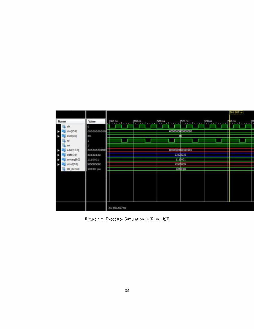
Figure 4.2: Processor Simulation in Xilinx ISE
38

Chapter 5
Xilinx ISE and Spartan-3
5.1 Introduction
In this we will discuss how to create a simple Xilinx ISE project based on theSpartan-3 Board. We will be implementing a simple decoder circuit that usesthe switches on the board as inputs and the eight LEDs as outputs. There areseveral parts to this tutorial. Part 1 shows the basics of creating a project inXilinx ISE. Part 2 shows how to create a PROM �le that can be written to thenon-volatile memory on the Spartan-3 board (because the FPGA's con�gurationis lost when power is turned o�). Part 3 shows how to then program the board.
5.1.1 Part 1: Starting a new Project
Start the Xilinx ISE 7.1i Project Navigator:Click Next.Select the device family, device, package, and speed grade, as shown here:
ClickClick Next.Click New Source.Select VHDL Module and enter �decoder� as the �le name:Click Next.You can now specify the inputs and outputs for the decoder. These will be
inserted into an automatically generated template for the VHDL �le. We haveone 3-bit input (�sel�) and one 8- bit output (�y�):
Click Next. You will be shown a summary window:Click Finish.Project Navigator now shows you a summary of the project:Click on the �decoder.vhd� tab below the summary window, or double-click
on �decoderbehaviorial� in the top left �Sources� pane.You will need to describe the behavior of the decoder using statements in the
architecture body. In this example we will use a conditional signal assignmentstatement:
39

Figure 5.1: Xilinx Window
40
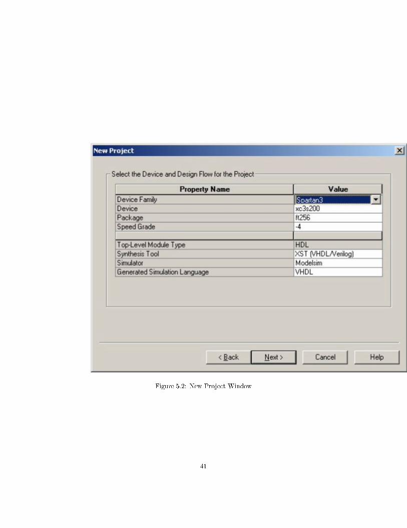
Figure 5.2: New Project Window
41

Figure 5.3: Project Source Properties Window
42

Figure 5.4: Module Nomenclature Window
43

Figure 5.5: Source De�ning Window
44
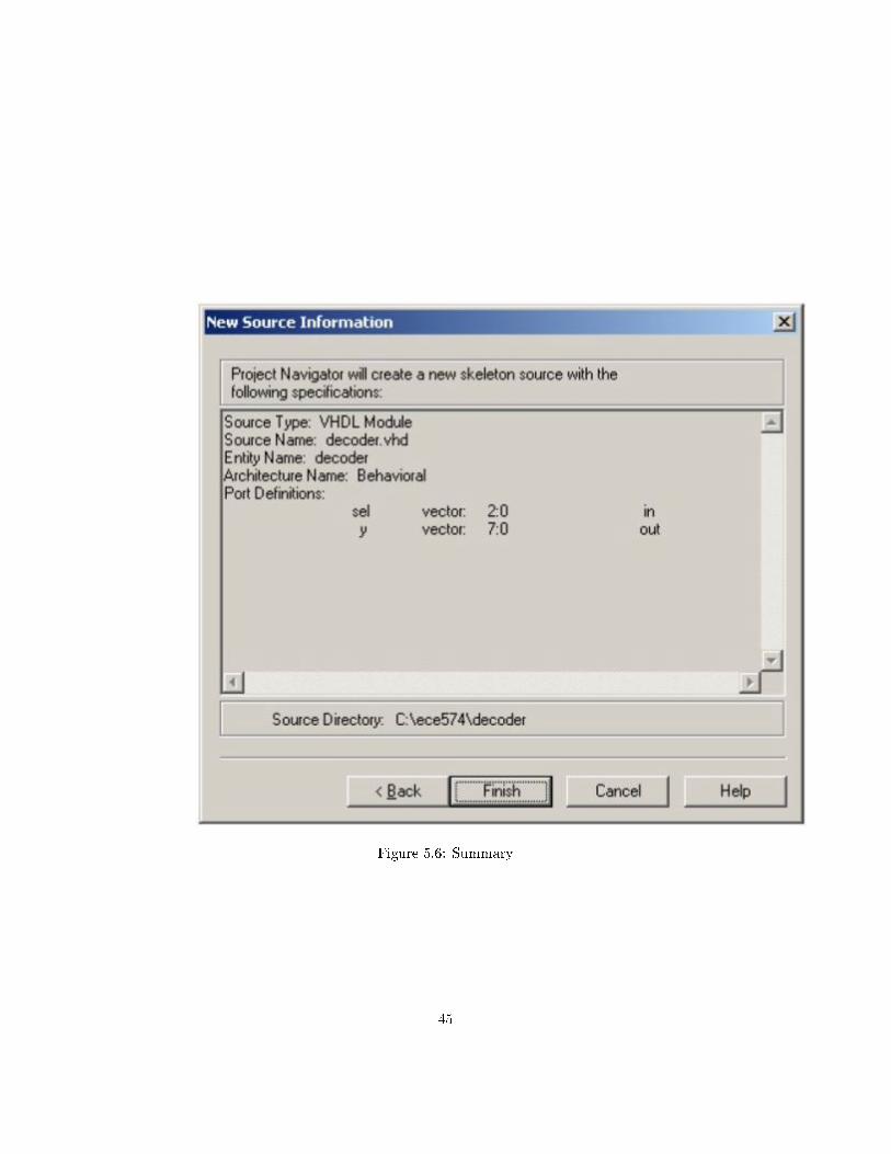
Figure 5.6: Summary
45

Figure 5.7: Project Navigator Window
46

Figure 5.8: Code Window
47

Before we can synthesize this design we need to specify what pins on theFPGA the inputs and outputs are connected to.
Double-Click on �Assign Package Pins� in the �Processes� pane in the left ofthe window.
Note: You may be asked to save the VHDL �le, and your design will bechecked for syntax errors (these will need to be �xed before you can proceed).
The tools will prompt you to create a UCF �le:Click Yes.The PACE editor will load:Click File Save followed by File Exit.
5.1.2 Part 2: Generating a PROM File
In this part of the chapter, we will see how to generate a PROM �le that canbe written to the Platform Flash on the Spartan-3 board, so that your FPGA'scon�guration is saved even when the board is powered down.
If you do not want to generate a PROM �le, you can skip directly to Part 3.However, in the interest of this tutorial we recommend you complete this partas well.
We assume you are continuing from Part 1 above and are still in ProjectNavigator:
Double-click on �Generate PROM, ACE, or JTAG File� in the �Processes�pane. You will notice that Project Navigator will execute the steps listedabove �Generate Programming File� (Synthesis and Implement Design) andmark them with a green checkmark as they complete.
The iMPACT tool will open and a wizard to create a new con�guration willopen.
Select PROM File:Click Next.Enter the PROM File Name (for example, �decoder_prom�):Click Next.Select the appropriate PROM (which is �xcf� / �xcf02s� for this board) from
the dropdown menus and click Add:Click Next.You will be shown a summary:Click Next.Click Add File.Select the �decoder.bit� �le and click Open.You can now click Finish.iMPACT will ask:Select Yes.You should then see iMPACT report successful �le generation:Before you close iMPACT, select File Save Project As. . .Save the con�guration under a �lename such as �decoder_prom.ipf�, but
do not use the default �lename of �decoder.ipf� (if you follow Part 2a below,remember this �lename).
48
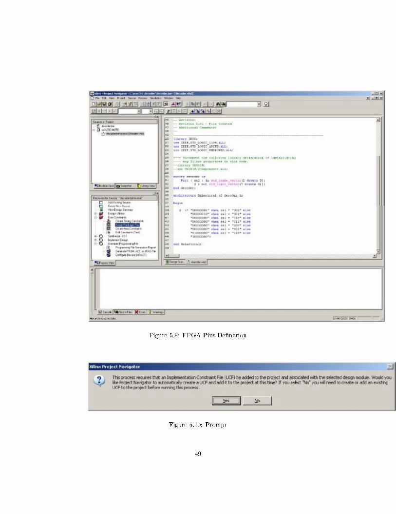
Figure 5.9: FPGA Pins De�nation
Figure 5.10: Prompt
49

Figure 5.11: Xilinx Pace
50

Figure 5.12: PROM Con�guration Files
51

Figure 5.13: Prepare PROM Files
52
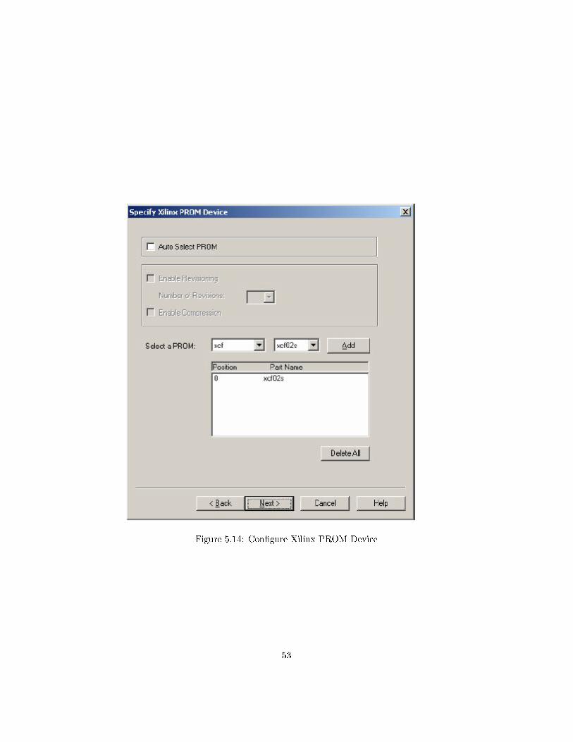
Figure 5.14: Con�gure Xilinx PROM Device
53

Figure 5.15: Summary Wizard
54

Figure 5.16: Add Files
55

Figure 5.17: Adding Source Bit Files
56

Figure 5.18: Adding Device
57

Figure 5.19: PROM File Generation
Figure 5.20: Final Output Window
58
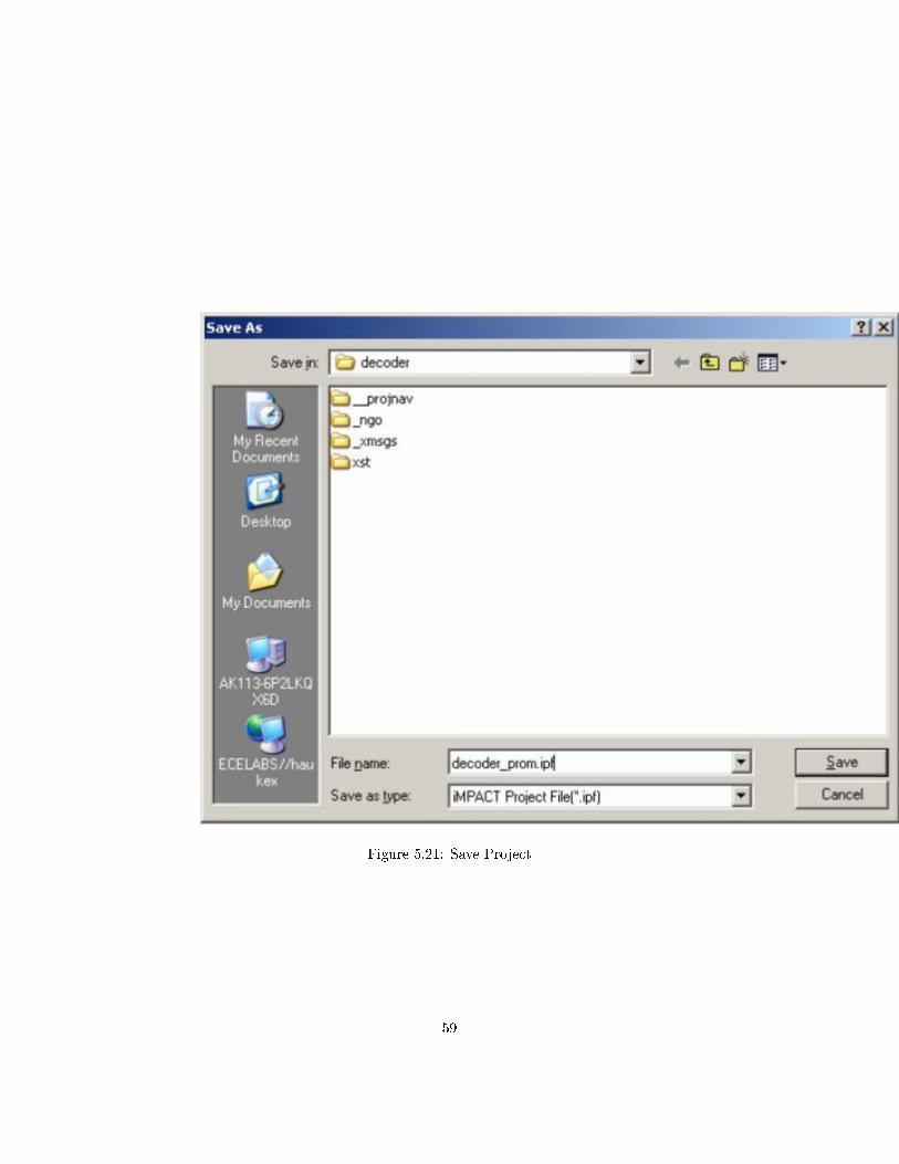
Figure 5.21: Save Project
59

You can now close iMPACT.
60

Bibliography
[1] Fundamentals of Logic Design with VHDL- Stephen Brown &Zvonko Vranesic
[2] Fundamentals of Logic Design with Verilog- Stephen Brown &Zvonko Vranesic
[3] VHDL Programming by Examples- Douglas L. Perry
[4] Verilog Digital System Design- Zinalabedin Navabi
[5] FPGA Prototyping by VHDL Examples - Xilinx Spartan-3 Ver-sion
61