robust hermetic packaging techniques for mems...
TRANSCRIPT

SANDIA REPORT
SAND2004-4755 Unlimited Release Printed October 2004 Robust Hermetic Packaging Techniques for MEMS Integrated Microsystems
Brian H. Stark, Junseok Chae, Andrew Kuo, Andrew Oliver*, and Khalil Najafi
Prepared by Sandia National Laboratories Albuquerque, New Mexico 87185 and Livermore, California 94550 Sandia is a multiprogram laboratory operated by Sandia Corporation, a Lockheed Martin Company, for the United States Department of Energy’s National Nuclear Security Administration under Contract DE-AC04-94AL85000. Approved for public release; further dissemination unlimited.
Issued by Sandia National Laboratories, operated for the United States Department of Energy by Sandia Corporation.
NOTICE: This report was prepared as an account of work sponsored by an agency of the United States Government. Neither the United States Government, nor any agency thereof, nor any of their employees, nor any of their contractors, subcontractors, or their employees, make any warranty, express or implied, or assume any legal liability or responsibility for the accuracy, completeness, or usefulness of any information, apparatus, product, or process disclosed, or represent that its use would not infringe privately owned rights. Reference herein to any specific commercial product, process, or service by trade name, trademark, manufacturer, or otherwise, does not necessarily constitute or imply its endorsement, recommendation, or favoring by the United States Government, any agency thereof, or any of their contractors or subcontractors. The views and opinions expressed herein do not necessarily state or reflect those of the United States Government, any agency thereof, or any of their contractors. Printed in the United States of America. This report has been reproduced directly from the best available copy. Available to DOE and DOE contractors from
U.S. Department of Energy Office of Scientific and Technical Information P.O. Box 62 Oak Ridge, TN 37831 Telephone: (865)576-8401 Facsimile: (865)576-5728 E-Mail: [email protected] ordering: http://www.osti.gov/bridge
Available to the public from
U.S. Department of Commerce National Technical Information Service 5285 Port Royal Rd Springfield, VA 22161 Telephone: (800)553-6847 Facsimile: (703)605-6900 E-Mail: [email protected] order: http://www.ntis.gov/help/ordermethods.asp?loc=7-4-0#online
2

SAND2004-4755 Unlimited Release
Printed March 2005
Robust Hermetic Packaging Techniques for MEMS Integrated Microsystems
Brian H. Stark, Junseok Chae, Andrew Kuo, Andrew Oliver*, and Khalil Najafi
Center for Wireless Integrated Microsystems, University of Michigan *Sandia National Laboratory
Advanced Microsystems Packaging Sandia National Laboratories
P.O. Box 5800 Albuquerque, New Mexico 87185-1076
Abstract
This work is the result of a Sandia National Laboratories LDRD funded fellowship at the University of Michigan. Although, guidance and suggestions were offered by Sandia, the work contained here is primarily the work of Brian H. Stark, and his advisor, Professor Khalil Najafi. Junseok Chae, Andrew Kuo, and their co-workers at the University of Michigan helped to record some of the data. The following is an abstract of their work. We have developed a vacuum packaging technology using a thick nickel film to seal MEMS structures at the wafer level. The package is fabricated in a three-mask process by electroplating a 40 micro-meter thick nickel film over an 8 micro-meter sacrificial photoresist that is removed prior to package sealing. Implementation of electrical feedthroughs in this process requires no planarization. The large release channel enables an 800x800 micro-meter package to be released in less than three hours. Several mechanisms, based upon localized melting and lead/tin solder bumping, for sealing the release channel have been investigated. We have also developed Pirani gauges, integrated with this package, which can be used to establish the hermeticity of the different sealing technologies. They have measured a sealing pressure of approximately 1.5 Torr. Our work differs from previous Pirani gauges in that we utilize a novel doubly anchored structure that stiffens the structural membrane while not substantially degrading performance in order to measure fine leak rates.
3

Intentionally Left Blank
4
Contents
Introduction ...........................................................................................................7 MicroPackages .....................................................................................................7 Pirani Gauges .....................................................................................................12 Experimental Pirani Gauge Results ....................................................................19 Discussion of Pirani Gauges...............................................................................23 5. Conclusions ....................................................................................................24 6. Acknowledgements.........................................................................................24 References .........................................................................................................25 Distribution: .........................................................................................................27
5

Figures
Figure 1: Diagram of doubly anchored Pirani gauge. 9 Figure 2: Thermal impedance and electrical resistance of the Pirani gauge vs. pressure. 9 Figure 3: Process for manufacturing vacuum-sealed Pirani gauges 9 Figure 4: Package after fabrication but prior to sealing. Note the 6 μm high fluidic
feedthroughs. 9 Figure 5: SEM of packaged Pirani gauge. Note the conformal covering of the
feedthroughs. This is accomplished without planarization. 10 Figure 6: Pirani gauge encased in micro Pb/Sn solder ball 10 Figure 7: Thermal impedance of Pirani gauges before and after sealing with
Pb/Sn solder bumps. 10 Figure 8: Picture of neural probe test structure 11 Figure 9: Schematic of Active Neural Probe Test Structure 11 Figure 10: Schematic of Localized CVD for packaging 11 Figure 11: Layers in SUMMIT V™ process 12 Figure 12: Diagram of polysilcon Pirani gauge made in SUMMiT VTM 13 Figure 13: Temperature Distribution in Resistively Heated Microbridge 14 Figure 14: Maximum length beams in each Layer 16 Figure 15: Cross Sections of Pirani Gauge Designs 17 Figure 16: Maximum Detectable Pressure as a function of design number 18 Figure 17: Minimum Detectable Pressure as a function of design number 18 Figure 18: Predicted Response of various designs to pressure changes 19 Figure 19: Setup Used to Test Pirani Gauges 21 Figure 20: Thermal Impedance Vs. Pressure 250 µm Beams 22 Figure 21: Device #5 Thermal Impedance Vs. Pressure for Different Lengths 22 Figure 22: Device #1 Thermal Impedance vs. Pressure for Different Lengths 23
Tables
Table 1: Poly Layer Thickness in SUMMIT V™ 15 Table 2: Oxide Layer Thickness in SUMMIT V™ 15 Table 3: Different Pirani gauge designs implemented 17 Table 4 TCR of Each Device 20
6
Introduction This work is the result of a Sandia National Laboratories LDRD funded fellowship at the University of Michigan. Although, guidance and suggestions were offered by Sandia, the work contained here is primarily the work of Brian H. Stark, and his advisor, Professor Khalil Najafi. Junseok Chae, Andrew Kuo, and their coworkers at the University of Michigan helped to record some of the data. The following is a report on their work. In the first year we developed a packaging technology that employs a thick nickel film to vacuum seal a MEMS structure at the wafer level. The package is fabricated in a three-mask process by electroplating a 40 micro-meter thick nickel film over an 8 micro-meter sacrificial photoresist that is removed prior to package sealing. Implementation of electrical feedthroughs in this process requires no planarization. The large release channel enables an 800x800 micro-meter package to be released in less than three hours. Several mechanisms, based upon localized melting and lead/tin solder bumping, for sealing the release channel have been investigated. Pirani gauges integrated with this package have been used to establish the hermeticity of the different sealing technologies and have measured a sealing pressure of approximately 1.5 Torr. For the second year we refined the design of the Pirani gauges and implemented them into Sandia’s SUMMiT VTM surface micromachining technology. The integrated Pirani gauge that we have developed is crucial to package characterization. Fabrication of surface micromachined Pirani gauges is complicated by the need for precise stress control to prevent thermal shorting to the substrate. Our work differs from previous Pirani gauges in that we utilize a novel doubly anchored structure that stiffens the structural membrane while not substantially degrading performance in order to measure fine leak rates.
MicroPackages For this project, we have developed a packaging technology that employs a thick nickel film to vacuum seal a MEMS structure at the wafer level. The package is fabricated in a 3-mask process by electroplating a 40-micron thick nickel film over an 8-micron sacrificial photoresist that is removed prior to package sealing. The large fluidic access port enables an 800x800 micro-meter package to be released in less than three hours. Implementation of electrical feedthroughs in this process requires no planarization. Device release is performed after the formation of the first level package. Several mechanisms, based upon localized melting and Pb/Sn solder bumping, for sealing low fluidic resistance feedthroughs have been investigated. This package has been fabricated with an integrated Pirani gauge to further characterize the different sealing technologies. These gauges have been used to establish the hermeticity of the different sealing technologies and have measured a sealing pressure of ~1.5Torr.
7

The process for manufacturing this package with an integrated Pirani gauge is shown in Figure 3. The Pirani gauge is defined in a 4-mask surface micromachined process that employs polysilicon both as a sacrificial material and for package feedthroughs. This is followed by deposition of an 8-micron thick sacrificial photoresist spacer that also defines a fluidic access port. This structure is then capped in 40-micron thick electroplated nickel. The photoresist and sacrificial polysilicon layer are then simultaneously etched in TMAH and dried in supercritical CO2. The polysilicon etch in the 800x800 μm package takes three hours and which is only about six times longer than unpackaged devices. The cleaning process in limited by etching the polysilicon, which dissolves at a rate of 0.75 μm/min inside the package, as compared to an etch rate of 1 μm/min in unpackaged devices. Figure 4 shows the package structure before sealing with a close-up of the fluidic access port. Figure 5 shows the polysilicon feedthroughs implemented in this process. Conformal covering of the feedthroughs occurs without the need for planarization. By increasing the vertical height of the fluidic access port from a few thousand Angstroms (previous work) to 6-8 microns (this work), the effective fluidic resistance into the package is dropped by at least three orders of magnitude. However, sealing this structure required extensive process development. The most promising method to seal the fluidic feedthrough utilizes Pb/Sn solder balls to encapsulate the package. After fabrication and release of the Pirani gauge, a 63Sn/37Pb solder paste was stenciled over the package by means of a custom stainless steel micro stencil. The package was then inserted into a vacuum chamber and heated past the soldering temperature (~230º C). The resultant structure (Figure 6) consists of a MEMS structure inside a cavity that is encased in solder. Figure 7 shows the thermal impedance of three different types of Pirani gauges before and after solder sealing. As the figure indicates, the thermal impedance increases after sealing, which is consistent with vacuum encapsulation. Based on the measure data, a pressure of ~1.5Torr exists inside the cavity. Currently, we are also working on measuring long term reliability of active neural probes packaged with electroplated gold. We have developed a test probe (Figure 8) that utilizes test transistors and resistors (Figure 9) to measure the survivability of active electronics during accelerated testing in phosphate buffered saline. These accelerated tests should commence in the next few months. We are also developing a thin film package that is compatible with MEMS made in a foundry process. We have proposed a technique, based upon localized heating of polysilicon ribs, to seal MEMS at the die level after production in a foundry process, such as SUMMiT VTM as shown in Figure 10. This work will be conducted in conjunction with Sandia and will take advantages of their extensive facilities and expertise.
8
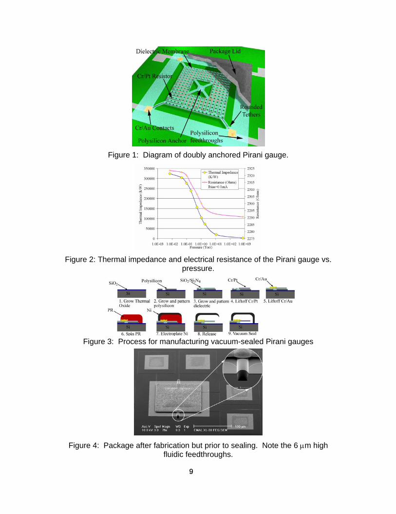
Figure 1: Diagram of doubly anchored Pirani gauge.
Figure 2: Thermal impedance and electrical resistance of the Pirani gauge vs.
pressure.
Figure 3: Process for manufacturing vacuum-sealed Pirani gauges
Figure 4: Package after fabrication but prior to sealing. Note the 6 μm high
fluidic feedthroughs.
9

Figure 5: SEM of packaged Pirani gauge. Note the conformal covering of the
feedthroughs. This is accomplished without planarization.
Figure 6: Pirani gauge encased in micro Pb/Sn solder ball
Figure 7: Thermal impedance of Pirani gauges before and after sealing with
Pb/Sn solder bumps.
10

Figure 8: Picture of neural probe test structure
Figure 9: Schematic of Active Neural Probe Test Structure
Figure 10: Schematic of Localized CVD for packaging
11
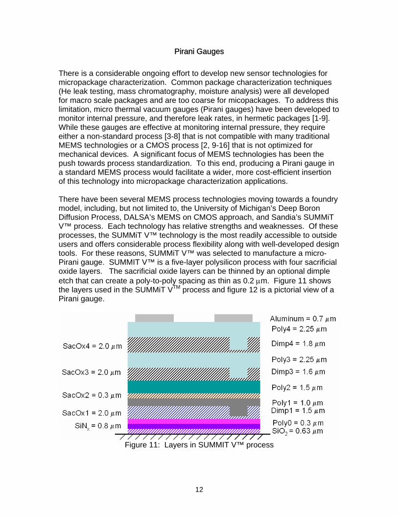
Pirani Gauges There is a considerable ongoing effort to develop new sensor technologies for micropackage characterization. Common package characterization techniques (He leak testing, mass chromatography, moisture analysis) were all developed for macro scale packages and are too coarse for micopackages. To address this limitation, micro thermal vacuum gauges (Pirani gauges) have been developed to monitor internal pressure, and therefore leak rates, in hermetic packages [1-9]. While these gauges are effective at monitoring internal pressure, they require either a non-standard process [3-8] that is not compatible with many traditional MEMS technologies or a CMOS process [2, 9-16] that is not optimized for mechanical devices. A significant focus of MEMS technologies has been the push towards process standardization. To this end, producing a Pirani gauge in a standard MEMS process would facilitate a wider, more cost-efficient insertion of this technology into micropackage characterization applications. There have been several MEMS process technologies moving towards a foundry model, including, but not limited to, the University of Michigan’s Deep Boron Diffusion Process, DALSA’s MEMS on CMOS approach, and Sandia’s SUMMiT V™ process. Each technology has relative strengths and weaknesses. Of these processes, the SUMMiT V™ technology is the most readily accessible to outside users and offers considerable process flexibility along with well-developed design tools. For these reasons, SUMMiT V™ was selected to manufacture a micro-Pirani gauge. SUMMIT V™ is a five-layer polysilicon process with four sacrificial oxide layers. The sacrificial oxide layers can be thinned by an optional dimple etch that can create a poly-to-poly spacing as thin as 0.2 μm. Figure 11 shows the layers used in the SUMMiT VTM process and figure 12 is a pictorial view of a Pirani gauge.
Figure 11: Layers in SUMMIT V™ process
12

Figure 12: Diagram of polysilcon Pirani gauge made in SUMMiT VTM
The design of a polysilicon Pirani gauge was first described by Mastrangelo in 1991 [4, 17-19]. Other Pirani gauges in the literature include Jacobs, Stark and Paul [20-22]. Mastrangelo established the model necessary to understand heat transfer in these devices. The shape of the gauge is a doubly clamped beam with electrical contacts at both ends and closely spaced heat sinks separated by a thin air gap as shown in Figure 12. Electrical current is driven through the device, causing it to heat. Cooling is accomplished by two mechanisms: heat transfer through the silicon (solid conduction) and heat transfer through the gas (gaseous conduction). Gaseous conduction is pressure dependent and varies according to the Knudsen number of the gas. As such, reducing the air gap spacing will increase the dynamic range of the gauge. The heat generated by the ohmic power dissipation, Po, is given as:
whlk
RIbPo
si
02
=
where Ib is the bias current, R0 is the room temperature resistance, ksi is the thermal conductivity of silicon, w is the width of the poly bridge, h is the bridge thickness, and l is the bridge length. The heat lost to gaseous conduction, L, is given as:
TCRdhdk
nkL
gapsi
air ∗−=
13
This gives a temperature distribution across the bridge, T(x) of:
( )( )( )
2cosh
2cosh1
le
lxe
e
dxT
−−
=
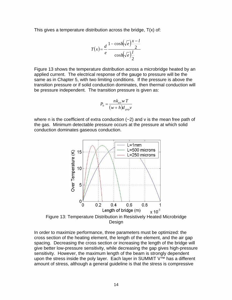
Figure 13 shows the temperature distribution across a microbridge heated by an applied current. The electrical response of the gauge to pressure will be the same as in Chapter 5, with two limiting conditions. If the pressure is above the transition pressure or if solid conduction dominates, then thermal conduction will be pressure independent. The transition pressure is given as:
( ) vdhw
wTnkP
gap
air
+=0
where n is the coefficient of extra conduction (~2) and v is the mean free path of the gas. Minimum detectable pressure occurs at the pressure at which solid conduction dominates gaseous conduction.
Figure 13: Temperature Distribution in Resistively Heated Microbridge
Design
In order to maximize performance, three parameters must be optimized: the cross section of the heating element, the length of the element, and the air gap spacing. Decreasing the cross section or increasing the length of the bridge will give better low-pressure sensitivity, while decreasing the gap gives high-pressure sensitivity. However, the maximum length of the beam is strongly dependent upon the stress inside the poly layer. Each layer in SUMMIT V™ has a different amount of stress, although a general guideline is that the stress is compressive
14

and between 5-8 MPa. For doubly clamped beams under compressive stress, buckling will occur when the stress is:
2
22
3L
Ehb
πσ −=
Figure 14 is a plot of buckling length versus intrinsic stress for poly1, poly2, and poly3. The thickness of the individual poly layers in SUMMIT V™ is given in Table 1. Table 2 gives interlayer spacing in the process. Beams may also deflect slightly before buckling. As such, long beams with narrow gaps may have limited sensitivity due to thermal shorting to the grounded case. There are a number of different sacrificial layers available in this process. To take into account beam warping, which varies from run to run, gauges were designed in several different layers. Table 1: Poly Layer Thickness in SUMMIT V™
Layer Thickness(μm) Poly0 0.3 Poly1 1.0 Poly2 1.5 Poly3 2.25 Poly4 2.25
Table 2: Oxide Layer Thickness in SUMMIT V™
Layer Gap Spacing(μm) SacOx1 2.0 Dimp1 1.5 SacOx2 0.3 SacOx3 2.0 Dimp3 0.4 SacOx4 2.0 Dimp4 0.2
15
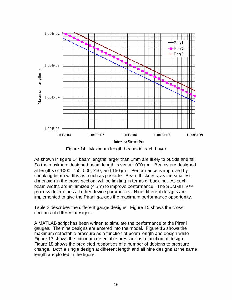
Figure 14: Maximum length beams in each Layer
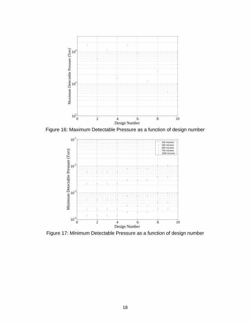
As shown in figure 14 beam lengths larger than 1mm are likely to buckle and fail. So the maximum designed beam length is set at 1000 μm. Beams are designed at lengths of 1000, 750, 500, 250, and 150 μm. Performance is improved by shrinking beam widths as much as possible. Beam thickness, as the smallest dimension in the cross-section, will be limiting in terms of buckling. As such, beam widths are minimized (4 μm) to improve performance. The SUMMIT V™ process determines all other device parameters. Nine different designs are implemented to give the Pirani gauges the maximum performance opportunity. Table 3 describes the different gauge designs. Figure 15 shows the cross sections of different designs. A MATLAB script has been written to simulate the performance of the Pirani gauges. The nine designs are entered into the model. Figure 16 shows the maximum detectable pressure as a function of beam length and design while Figure 17 shows the minimum detectable pressure as a function of design. Figure 18 shows the predicted responses of a number of designs to pressure change. Both a single design at different length and all nine designs at the same length are plotted in the figure.
16
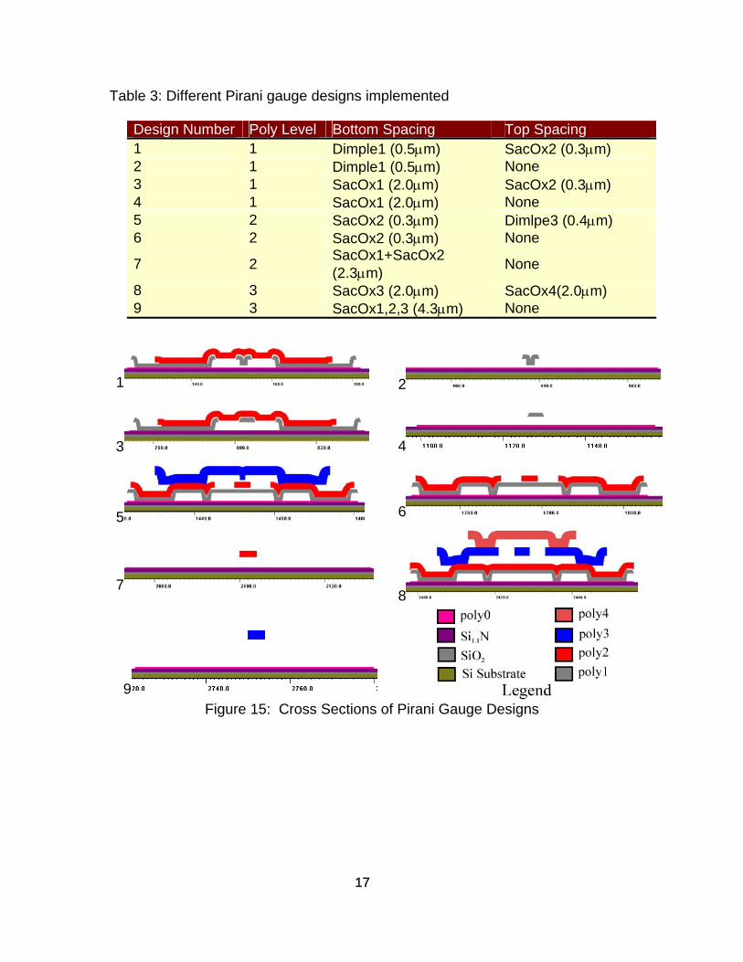
Table 3: Different Pirani gauge designs implemented
Design Number Poly Level Bottom Spacing Top Spacing 1 1 Dimple1 (0.5μm) SacOx2 (0.3μm) 2 1 Dimple1 (0.5μm) None 3 1 SacOx1 (2.0μm) SacOx2 (0.3μm) 4 1 SacOx1 (2.0μm) None 5 2 SacOx2 (0.3μm) Dimlpe3 (0.4μm) 6 2 SacOx2 (0.3μm) None
7 2 SacOx1+SacOx2 (2.3μm) None
8 3 SacOx3 (2.0μm) SacOx4(2.0μm) 9 3
17
None SacOx1,2,3 (4.3μm)
2 1
3 4
5 6
8 7
9 Figure 15: Cross Sections of Pirani Gauge Designs
0 2 4 6 8 10102
103
104
Max
imum
Det
ecta
ble
Pres
sure
(T
orr)
Design Number Figure 16: Maximum Detectable Pressure as a function of design number
0 2 4 6 8 1010-4
10-3
10-2
10-1
Min
imum
Det
ecta
ble
Pres
sure
(T
orr)
Design Number
150 microns250 microns500 microns750 microns1000 microns
Figure 17: Minimum Detectable Pressure as a function of design number
18

Figure 18: Predicted Response of various designs to pressure changes
Experimental Pirani Gauge Results
Recently, the Pirani gauges have been tested at the University of Michigan and we are including those results here. The devices were fabricated in the SUMMiT VTM process at Sandia National Laboratories on reticle set 416 module 8. To obtain the TCR, we initially tested each device and plotted the resistance vs. temperature. From this plot, we obtained the slope and the intercept and from the slope over the intercept we calculated the TCR. The TCRs for each device are shown in Table 3. The Pirani gauges are characterized with the system shown in Figure 19.
19

Table 4 TCR of Each Device
Poly 31.28 × 10³Device #9
Poly 31.33 × 10³Device #8
Poly 20.59 × 10³Device #7
Poly 20.59 × 10³Device #6
Poly 20.77 × 10³Device #5
Poly 11.26 × 10³Device #4
Poly 11.23 × 10³Device #3
Poly 11.30 × 10³Device #2
Poly 11.22 × 10³Device #1
Structural layerTCR [ppm/°C]
Poly 31.28 × 10³Device #9
Poly 31.33 × 10³Device #8
Poly 20.59 × 10³Device #7
Poly 20.59 × 10³Device #6
Poly 20.77 × 10³Device #5
Poly 11.26 × 10³Device #4
Poly 11.23 × 10³Device #3
Poly 11.30 × 10³Device #2
Poly 11.22 × 10³Device #1
Structural layerTCR [ppm/°C]
The existing setup uses a program in LabView to control a current source (Keithley 225A) and read voltage measurements off of a HP 34401A DVM, via GPIB. Initially, the thermal impedance extractor passes a small current through the device and measures the voltage (four point probe measurement). This four point probe measurement is used to set the R0. After this is set, the program continuously makes 4 point probe measurements while increasing the current each time. When the program reaches a certain temperature, the program will stop and calculate the thermal impedance. The way the program calculates the thermal impedance is by taking the voltage and dividing it by the current to determine the resistance of the device. The resistance is subsequently converted into a temperature value by multiplying by the TCR. The program will then plot the change in temperature against the change in power. From this graph, we are able to determine the line of best fit for our data, and the slope of this line is the thermal impedance. The thermal impedance varies from 1000K/W at atmospheric pressure to more than 320,000K/W at 10mTorr.
20
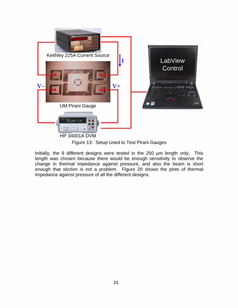
UM Pirani Gauge
Keithley 225A Current SourceI
V+V−
LabViewControl
HP 34001A DVM Figure 13: Setup Used to Test Pirani Gauges
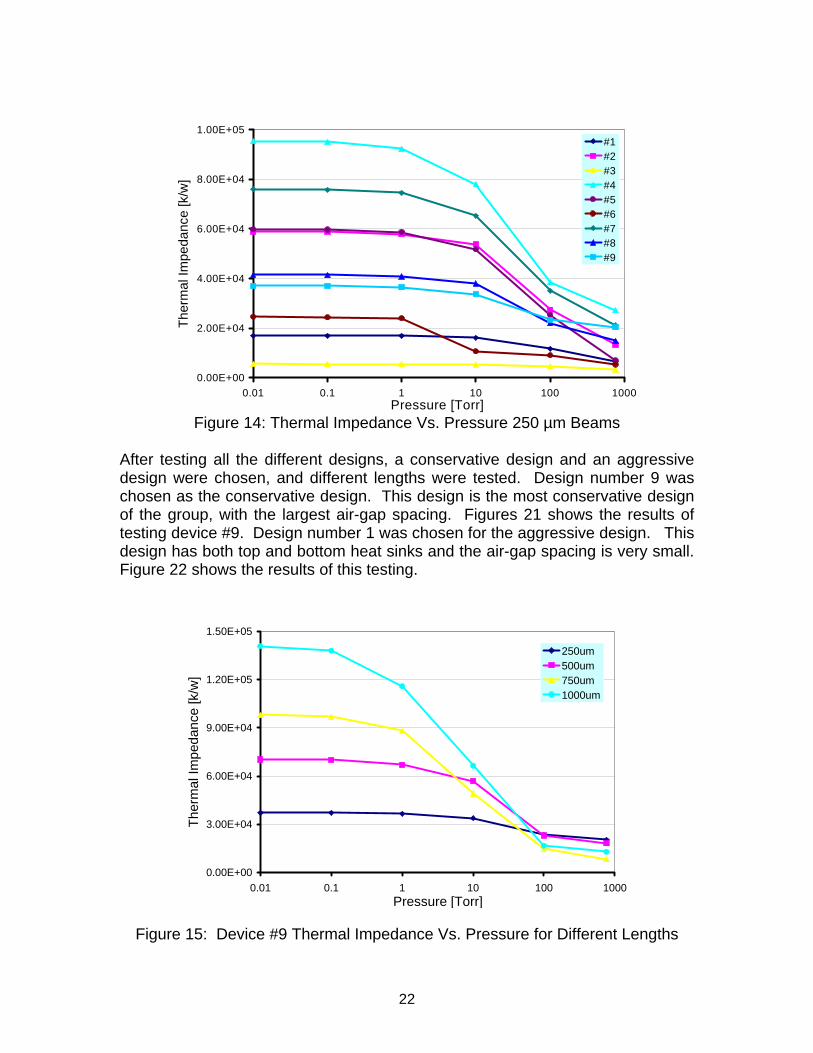
Initially, the 9 different designs were tested in the 250 µm length only. This length was chosen because there would be enough sensitivity to observe the change in thermal impedance against pressure, and also the beam is short enough that stiction is not a problem. Figure 20 shows the plots of thermal impedance against pressure of all the different designs.
21
0.00E+00
2.00E+04
4.00E+04
6.00E+04
8.00E+04
1.00E+05
0.01 0.1 1 10 100 1000Pressure [Torr]
Ther
mal
Impe
danc
e [k
/w]
#1#2#3#4#5#6#7#8#9
Figure 14: Thermal Impedance Vs. Pressure 250 µm Beams
After testing all the different designs, a conservative design and an aggressive design were chosen, and different lengths were tested. Design number 9 was chosen as the conservative design. This design is the most conservative design of the group, with the largest air-gap spacing. Figures 21 shows the results of testing device #9. Design number 1 was chosen for the aggressive design. This design has both top and bottom heat sinks and the air-gap spacing is very small. Figure 22 shows the results of this testing.
0.00E+00
3.00E+04
6.00E+04
9.00E+04
1.20E+05
1.50E+05
0.01 0.1 1 10 100 1000Pressure [Torr]
Ther
mal
Impe
danc
e [k
/w]
250um500um750um1000um
Figure 15: Device #9 Thermal Impedance Vs. Pressure for Different Lengths
22

0.00E+00
1.00E+04
2.00E+04
3.00E+04
4.00E+04
5.00E+04
6.00E+04
7.00E+04
8.00E+04
9.00E+04
0.01 0.1 1 10 100 1000Pressure [Torr]
Ther
mal
Impe
danc
e [k
/W]
250 um500um750 um1000 um
Figure 16: Device #1 Thermal Impedance vs. Pressure for Different Lengths
Discussion of Pirani Gauges Overall, it appears that when comparing all the designs directly at 250µm length, there are no benefits to the top heat sink. Rather, it seems that the more aggressive designs demonstrated worse performance than the more conservative designs. One possibility for this is that the top casing that is supposed to help to dissipate heat is actually causing the heat to be trapped inside the casing. When a very conservative design (design 9) was tested for all the different lengths, the longer lengths were much more sensitive than the shorter lengths. As shown in figure 21 the 1000µm device was more than one order of magnitude more sensitive than the 250µm device. Oddly, during testing, the more aggressive design (design 1) at longer lengths performed worse than the medium-length devices. This is most likely because the devices shorted to the thermally-grounded casing as they were heated. This caused the performance of the device to be decreased. Therefore in figure 22 the 750 and the 1000 µm devices did not perform as well as the 500 µm devices. In less aggressive designs with a greater top and bottom spacing, it is reasonable to predict that this problem will not be present. Most of the Pirani gauges fabricated in the SUMMIT VTM have been tested and characterized. The test data demonstrates that the thermally grounded casing on the top and bottom had very little effect on the devices, and in some cases actually hurt performance. In testing the different lengths, conservative devices with no grounded casing performed better for different lengths, while aggressive
23

designs with small gaps and thermally-grounded casing did not exhibit this trend. This is most likely because the beam deflected and shorted to the casing. Future work on this area includes testing other designs that are neither aggressive nor conservative in order to gauge their performance.
Conclusions This report describes work done at the University of Michigan on micropackages and Pirani gauges as part of an LDRD funded university fellowship. The packages have been demonstrated to be hermetic with a base pressure of 1.5 Torr. The Pirani gauges have a measured sensitivity below 10 mTorr.
Acknowledgments This report describes work done at the University of Michigan on micropackages and Pirani gauges as part of an LDRD funded University fellowship. Much of the writing was done by Brian Stark, fellowship student, and his co-workers at the University of Michigan. Professor Khalil Najafi acted as the faculty advisor. Cathy Morgan, SNL staff member assigned as an integration engineer, did much of the leg work in setting up the fellowship on the Michigan end. Jay Jakubczak, Sandia Point of Contact for the University of Michigan’s WIMS Center, helped set up the fellowship on the Sandia end. Rick Stulen, University of Michigan Campus Executive, funded fellowship. Some of the work was also paid for by Sandia National Laboratories’ MESA Institute program through Regan Stinnett, MESA Institute manager..
24
References [1] J. Chae, B. H. Stark, and K. Najafi, "A Micromachined Pirani Gauge for Vacuum Package Characterization," Proceedings of the 17th IEEE International Conference on Microelectromechanical Systems (MEMS), Maastricht, The Netherlands, pp. 2004. [2] J. J. v. Baar, R. J. Wiegerink, T. S. J. Lammerink, J. W. Berenschot, and G. J. M. Krijen, "Combined-Pirani/bending membrane-pressure sensor," Proceedings of the 15th IEEE International Conference on Microelectromechanical Systems, Las Vegas, NV, pp. 328-331, 2002. [3] B. C. S. Chou, J.-S. Shie, and Y.-M. Chen, "Highly sensitive Pirani vacuum gauge," International Conference on Solid State Sensors and Actuators, and Eurosensors IX, Proceedings, vol. 2, pp. 167-170, 1995. [4] C. H. Mastrangelo and R. S. Muller, "Fabrication and performance of a fully integrated micro -Pirani pressure gauge with digital readout," 6th International Conference on Solid-State Sensors and Actuators (Transducers '91), vol. 91, pp. 245-248, 1991. [5] O. Paul, A. Haberli, P. Malcovati, and H. Baltes, "Novel integrated thermal pressure gauge and read-out circuit by CMOS IC technology," Technical Digest International Electron Devices Meeting, pp. 131-134, 1994. [6] J.-S. Shie, B. C. S. Chou, and Y.-M. Chen, "High Performance Pirani Vacuum Gauge," Journal of Vacuum Science and Technology A, vol. 13, pp. 2972-2979, 1995. [7] B. H. Stark, Y. Mei, C. Zhang, and K. Najafi, "A Doubly Anchored Surface Micromachined Pirani Gauge for Vacuum Package Characterization," Proceedings of the 16th IEEE International Conference on Microelectromechanical Systems (MEMS), Kyoto, Japan, pp. 506-9, 2003. [8] B. H. Stark, Y. Mei, C. Zhang, and K. Najafi, "A Doubly-Anchored Surface Micromachined Pirani Gauge for Vacuum Monitoring," Submitted to JMEMS, 2003. [9] N. R. Swart and A. Nathan, "Integrated CMOS polysilicon coil-based micro-Pirani gauge with high heat transfer efficiency," Technical Digest International Electron Devices Meeting, pp. 135-138, 1994. [10] Y. Ma, A. M. Robinson, R. P. W. Lawson, and W. Allegretto, "CMOS micromachined low power microlamp vacuum sensor," Proceedings of the Canadian Conference on Electrical and Computer Engineering, pp. 971-975, 2000. [11] S. Leclerc, R. Antaki, and J. F. Currie, "Novel simple and complementary metal-oxide-semiconductor-compatible membrane release design and process for thermal sensors," Journal of Vacuum Science & Technology A: Vacuum, Surfaces, and Films, vol. 16, pp. 876-880, 1998. [12] H. Baltes, O. Paul, and O. Brand, "Micromachined thermally based CMOS microsensors," Proceedings of the IEEE, vol. 86, pp. 1660-1678, 1998.
25
[13] A. Haberli, O. Paul, P. Malcovati, M. Faccio, F. Maloberti, and H. Baltes, "CMOS integration of a thermal pressure sensor system," Proceedings of the IEEE International Symposium on Circuits and Systems, pp. 377-380, 1996. [14] M. A. Gajda and H. Ahmed, "Applications of thermal silicon sensors on membranes," Sensors and Actuators, A: Physical, vol. 49, pp. 1-9, 1995. [15] O. Paul, A. Haberli, P. Malcovati, and H. Baltes, "Novel integrated thermal pressure gauge and read-out circuit by CMOS IC technology," Proceedings of the International Electron Devices Meeting, pp. 131-134, 1994. [16] N. R. Swart and A. Nathan, "Integrated CMOS polysilicon coil-based micro-Pirani gauge with high heat transfer efficiency," International Electron Devices Meeting, pp. 135-138, 1994. [17] C. H. Mastrangelo, "Vacuum-sealed silicon micromachined incandescent light source," Proceedings of the International Electron Devices Meeting, pp. 1989. [18] C. H. Mastrangelo, Ph.D. Thesis, Thermal Applications of Microbridges, in Electrical Engineering and Computer Science at The University of California, Berkeley, CA, 1991. [19] C. H. Mastrangelo, R. S. Muller, and S. Kumar, "Microfabricated Incandescent Lamps," Applied Optics, vol. 30, pp. 868-873, 1993. [20] D. Jacobs and D. Baker, "Miniaturized thin film thermal vacuum sensor," Journal of Vacuum Science and Technology A, vol. 13, pp. 2980-5, 1995. [21] B. Stark, et. al., “A Doubly Anchored Surface Micromachined Pirani Gauge for Vacuum Package Characterization,” Proceedings of MEMS 2003, Kyoto, Japan, January 19-23, 2003 [22]O. Paul,., et al., "Novel integrated thermal pressure gauge and read-out circuit by CMOS IC technology." Proceedings of IEDM, pp. 131-134, 1994.
26
Distribution: 1 MS1071 Jay Jakubczak 1703 1 MS9004 Rick Stulen 8100 1 MS0865 Regan Stinnet 1903 1 MS1310 Bernie Jokiel 1745 1 MS0889 Jon Custer 1851 1 MS1076 Thomas Fischer 1745 1 MS1073 Steve Rohde 17382 1 MS1310 Maarten deBoer 1762 1 MS0867 Robert M. Ferrizz 14405 1 MS1076 Joshua J. Whiting 17381 1 MS0123 Donna L. Chavez 1011 5 MS1076 Andrew D. Oliver 1745 1 MS1080 Harold D. Stewart 1749 1 MS1080 James Allen 1769 1 MS9018 Central Technical File 8945-1 2 MS0899 Technical Library 9616
27