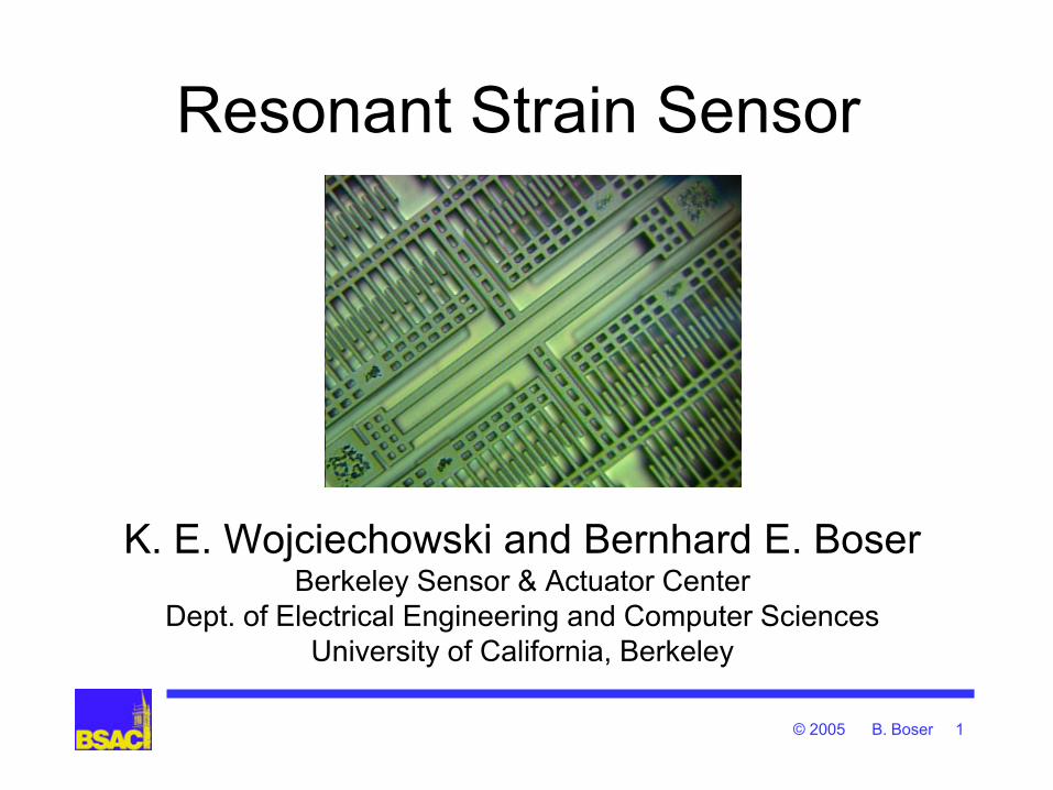
resonant strain sensor
TRANSCRIPT
© 2005 B. Boser 1
Resonant Strain Sensor
K. E. Wojciechowski and Bernhard E. Boser Berkeley Sensor & Actuator Center
Dept. of Electrical Engineering and Computer Sciences
University of California, Berkeley
© 2005 B. Boser 2
Outline
• Strain sensor
• Resonant force sensing
• Oscillator analysis
– Phase and frequency noise
– Design for minimum noise
• Oscillator sustaining circuit
• Frequency-to-digital conversion
• Conclusions
© 2005 B. Boser 3
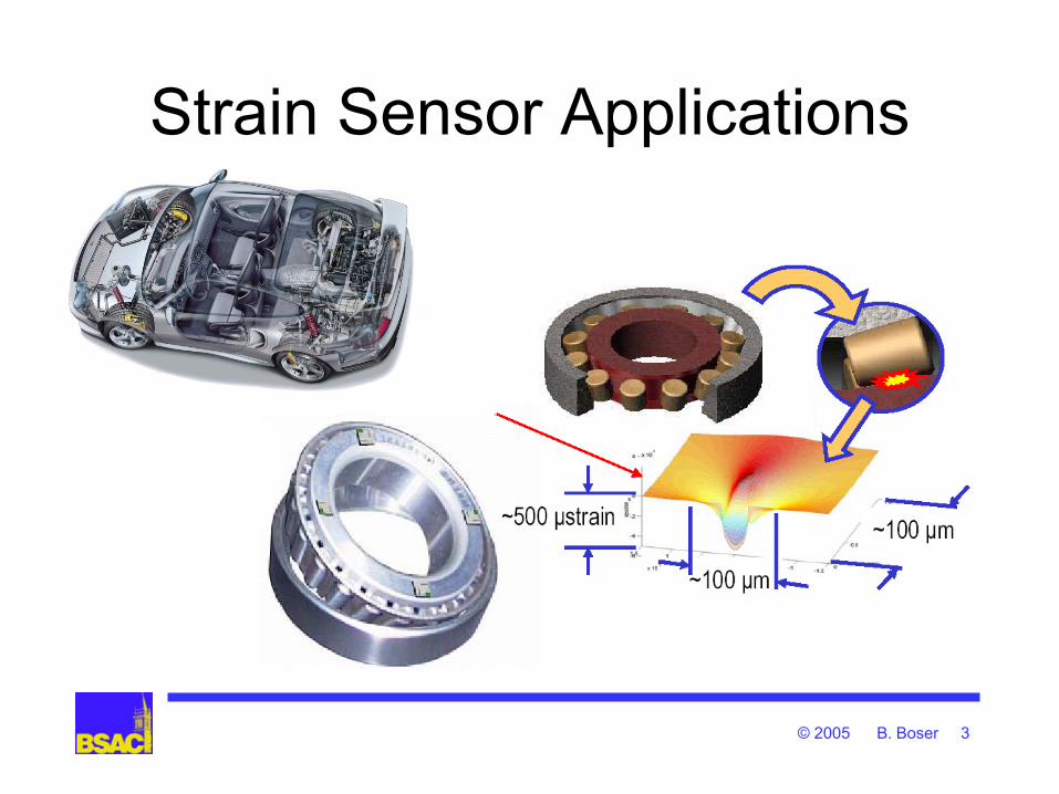
Strain Sensor Applications
© 2005 B. Boser 4
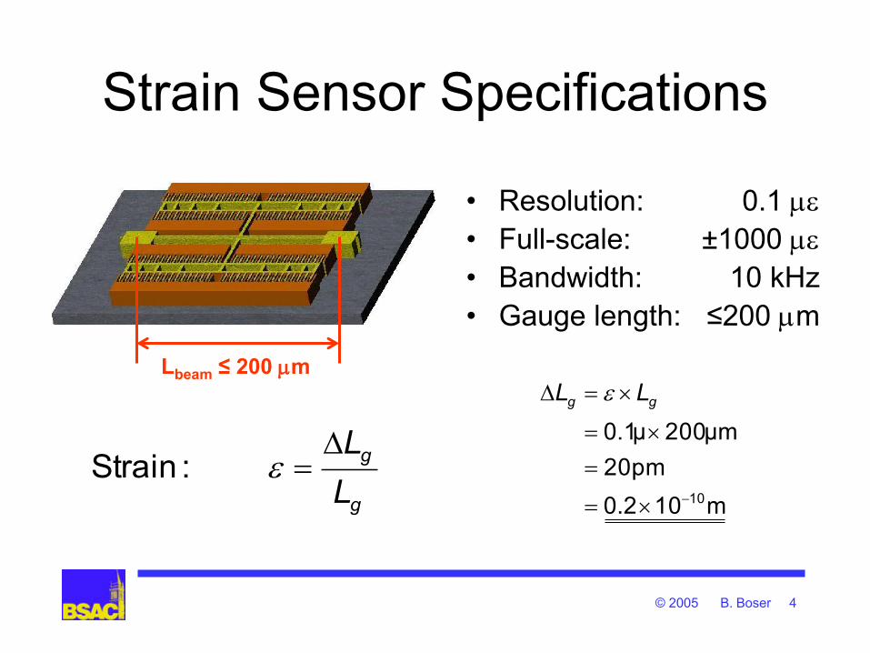
Strain Sensor Specifications
Lbeam ≤ 200 mm
g
g
L
L :Strain
• Resolution: 0.1 m
• Full-scale: ±1000 m
• Bandwidth: 10 kHz
• Gauge length: ≤200 mm
m102.0
20pm
μm200μ1.0
10
gg LL
© 2005 B. Boser 5
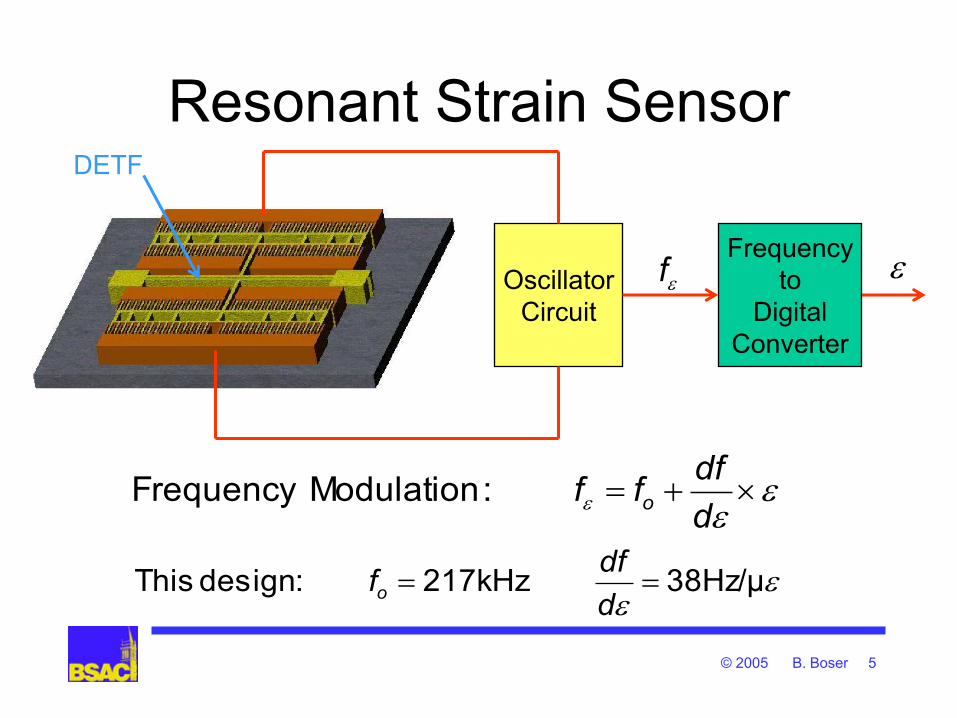
Resonant Strain Sensor
d
dfff o :Modulation Frequency
38Hz/μ 217kHz :design This d
dffo
Oscillator
Circuit
Frequency
to
Digital
Converter
f
DETF
© 2005 B. Boser 6
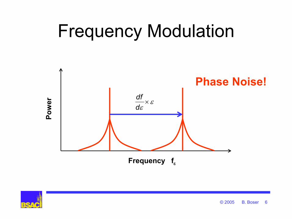
Frequency Modulation P
ow
er
Frequency f
d
df
Phase Noise!

© 2005 B. Boser 7
Phase Noise
1 10 100 1 103
1 104
1 105
130
120
110
100
90
80
7070
130
dB10 L f L o f co
100f cof co
100
f
Frequency Offset f [Hz]
Ph
as
e N
ois
e D
en
sit
y
L(
f)
[dB
c/H
z]
Power-Carrier
Bandwidth / Power-NoisefL
Bandwidth f
Noise-Power / Bandwidth
Lnear(f)
Lfar
© 2005 B. Boser 8
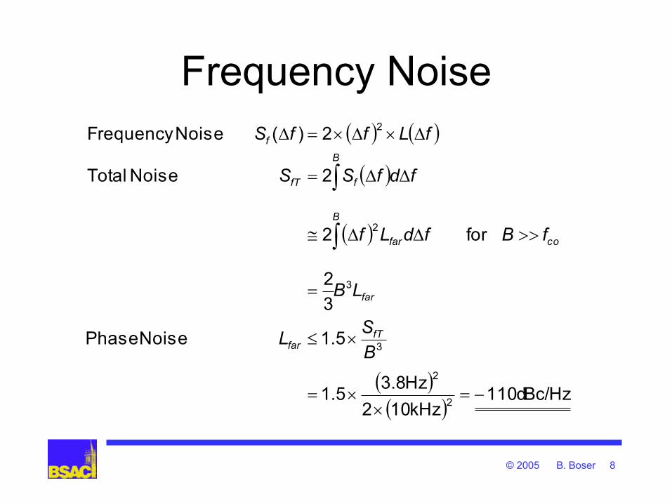
Frequency Noise
Bc/Hzd110kHz102
Hz8.35.1
5.1 Noise Phase
3
2
for 2
2 Noise Total
2)( NoiseFrequency
2
2
3
3
2
2
B
SL
LB
fBfdLf
fdfSS
fLffS
fTfar
far
co
B
far
B
ffT
f
© 2005 B. Boser 9
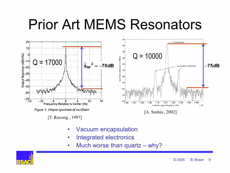
Prior Art MEMS Resonators
• Vacuum encapsulation
• Integrated electronics
• Much worse than quartz – why?
[T. Roessig , 1997]
dB702
NF
[A. Seshia , 2002]
Q = 10000 Q = 17000
dB75

© 2005 B. Boser 10
MEMS Oscillator Noise Roessig
1997
Nguyen
1999
Seshia
2002
Seth
2004
Goal
(This Work)
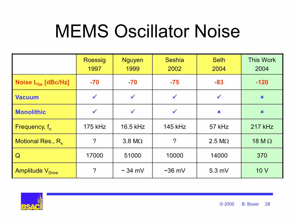
Noise Lfar [dBc/Hz] -70 -70 -75 -83 < -110
Vacuum
Monolithic
Frequency, fo 175 kHz 16.5 kHz 145 kHz 57 kHz 217 kHz
Motional Res., Rx ? 3.8 M ? 2.5 M
Q 17000 51000 10000 14000
Amplitude VDrive ? ~ 34 mV ~36 mV 5.3 mV
Need oscillator with 1000x lower noise than prior art!
© 2005 B. Boser 11
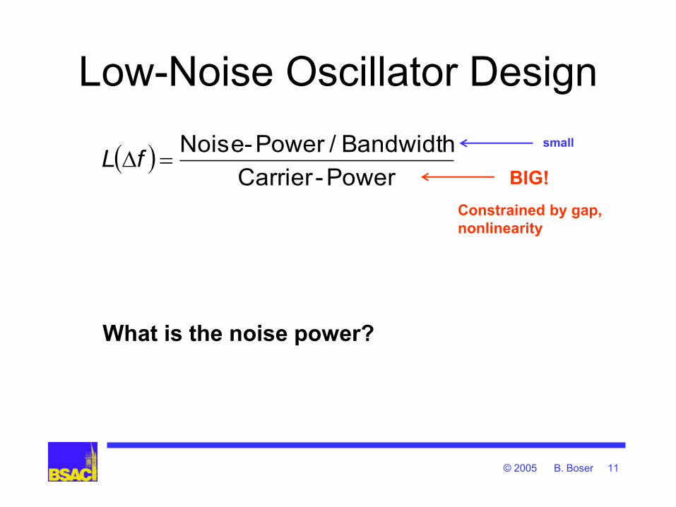
Low-Noise Oscillator Design
Power-Carrier
Bandwidth / Power-NoisefL
BIG!
small
What is the noise power?
Constrained by gap,
nonlinearity
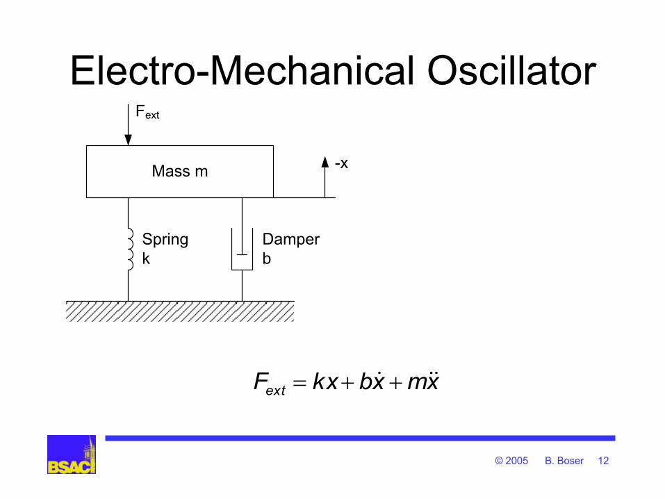
© 2005 B. Boser 12
Mass m
Spring
k
Damper
b
-x
Fext
Electro-Mechanical Oscillator
xmxbkxFext

© 2005 B. Boser 13
Mass m
Spring
k
Damper
b
-x
V
Fext
Cx
Lx
Rx
Electro-Mechanical Oscillator
xmxbkxFext
© 2005 B. Boser 14
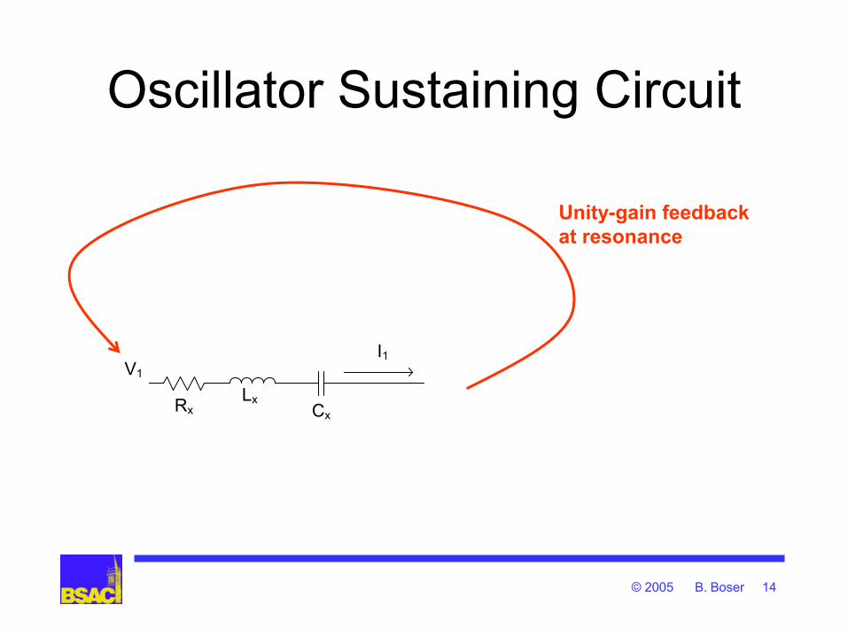
Oscillator Sustaining Circuit
Rx Lx
Cx
V1
I1
Unity-gain feedback
at resonance
© 2005 B. Boser 15
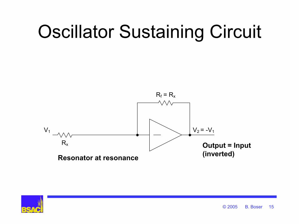
Oscillator Sustaining Circuit
Rx
Rf = Rx
V1 V2 = -V1
Resonator at resonance
Output = Input
(inverted)
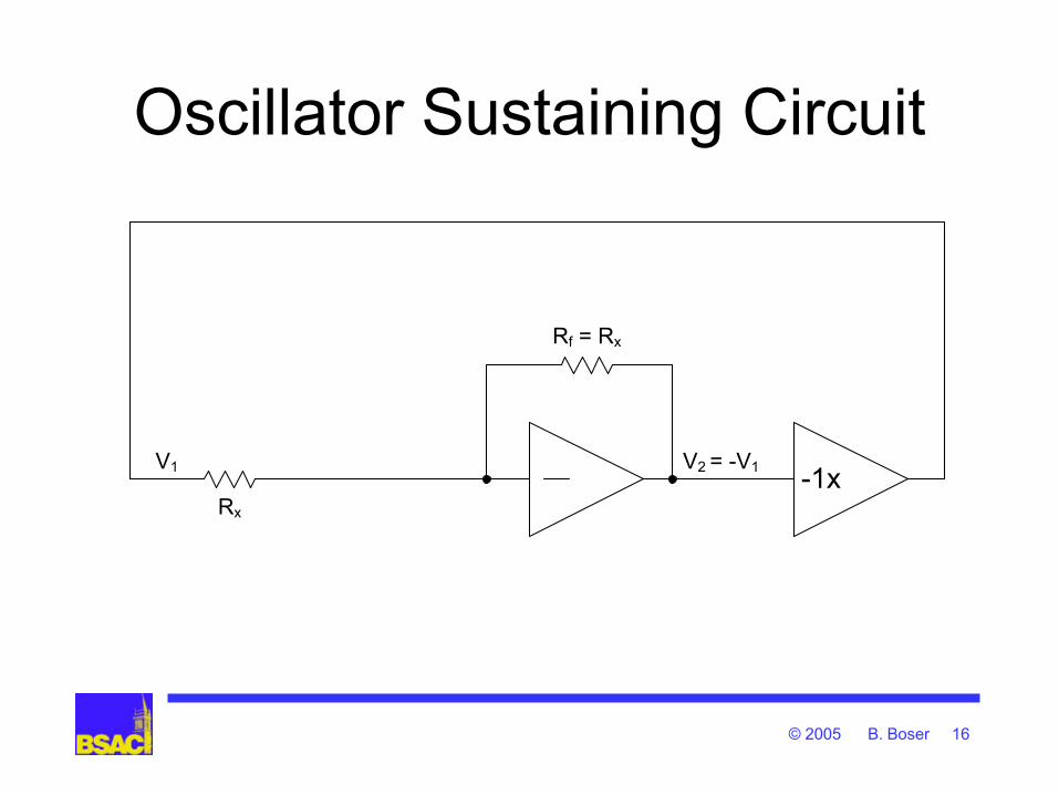
© 2005 B. Boser 16
Oscillator Sustaining Circuit
Rx
Rf = Rx
V1 V2 = -V1-1x

© 2005 B. Boser 17
Oscillator Noise Voltage
Rx
Rf = Rx
V1 V2 = -V1-1x
+
+
4kBTrRxf
4kBTrRxf
dffQ
fRTkv oxRBn
2
2
12
214High Q?

© 2005 B. Boser 18
Phase Noise
near
far
L
o
LoB
rB
o
oB
rB
oB
x
n
f
f
xk
Tk
fQ
fQ
xk
Tk
Q
xk
Rv
fL
2
2
2
2
spring in storedenergy
2
2
1
2
22
221
2
oscillator to delivered power
power-noise
tradeoff
(for high bandwidth optimal Q < 100)
for given mechanical amplitude
Qxk
TkL
oB
rBfar
2
2
2
2 2
14
f
f
Qxk
TkL o
oB
rBnear
© 2005 B. Boser 19
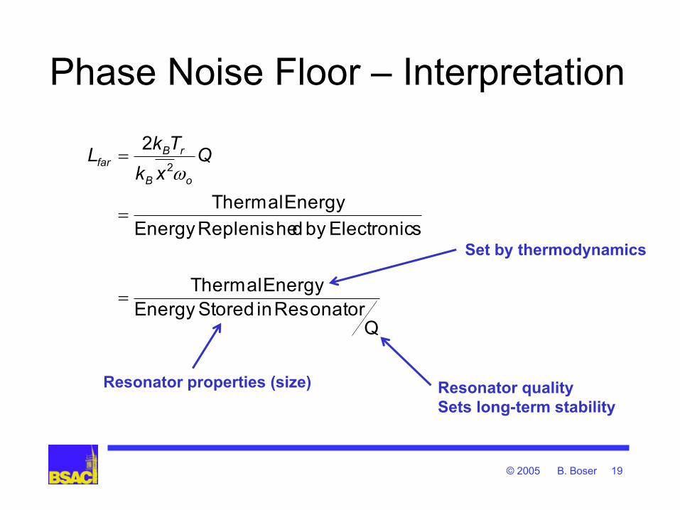
Phase Noise Floor – Interpretation
QResonator in StoredEnergy
Energy Thermal
sElectronicby dReplenisheEnergy
Energy Thermal
22
Qxk
TkL
oB
rBfar
Set by thermodynamics
Resonator properties (size) Resonator quality
Sets long-term stability

MEMS versus Quartz Resonators
1. Maximum power limited in “small”
MEMS oscillators – Increasing resonant frequency helps
– Bulk acoustic waves store more energy
2. High motional impedance Rx – Loaded Q ≈ intrinsic Q
© 2005 B. Boser 20
© 2005 B. Boser 21
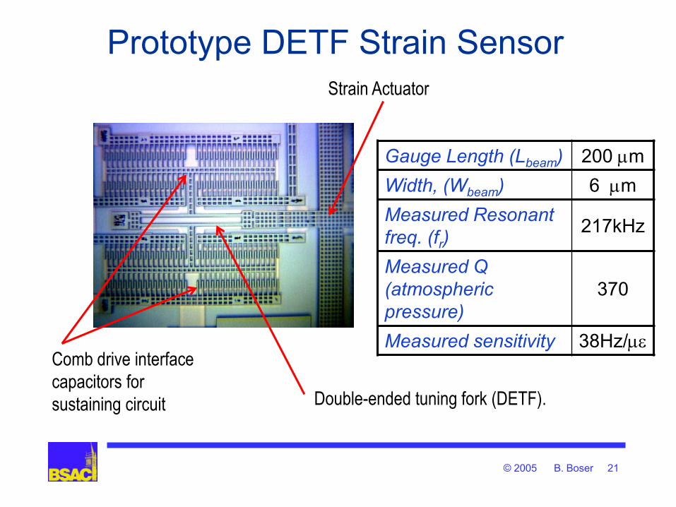
Prototype DETF Strain Sensor
Double-ended tuning fork (DETF).
Strain Actuator
Comb drive interface
capacitors for
sustaining circuit
Gauge Length (Lbeam) 200 mm
Width, (Wbeam) 6 mm
Measured Resonant
freq. (fr) 217kHz
Measured Q
(atmospheric
pressure)
370
Measured sensitivity 38Hz/m
© 2005 B. Boser 22
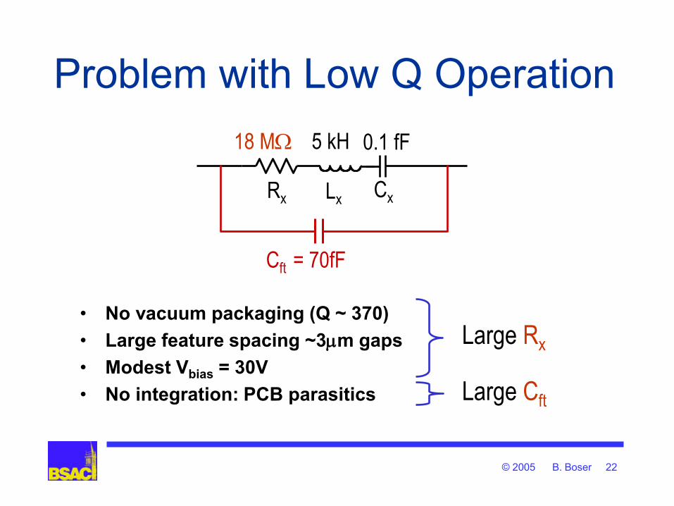
Problem with Low Q Operation
• No vacuum packaging (Q ~ 370)
• Large feature spacing ~3mm gaps
• Modest Vbias = 30V
• No integration: PCB parasitics
Large Rx
18 M 5 kH 0.1 fF
Rx Lx Cx
Cft = 70fF
Large Cft
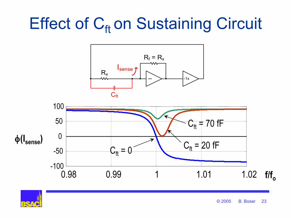
© 2005 B. Boser 23
Effect of Cft on Sustaining Circuit
Rx
Rf = Rx
-1x
Cft
Isense
(Isense)
f/fo
Cft = 0
0.98 0.99 1 1.01 1.02 -100
-50
0
50
100
Cft = 70 fF
Cft = 20 fF
© 2005 B. Boser 24
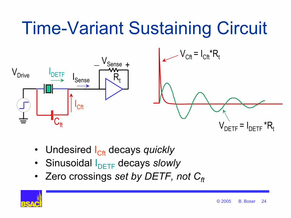
Time-Variant Sustaining Circuit
• Undesired ICft decays quickly
• Sinusoidal IDETF decays slowly
• Zero crossings set by DETF, not Cft
VDrive
Cft
IDETF
ICft
VDETF = IDETF *Rt
VCft = ICft*Rt
ISense Rt
VSense +

© 2005 B. Boser 25
Time-Variant Oscillator (TVO) Itot IRES
VDrive
Cft
Ift comparator
Itot
time
IRes
Ift
time
VDrive
© 2005 B. Boser 26
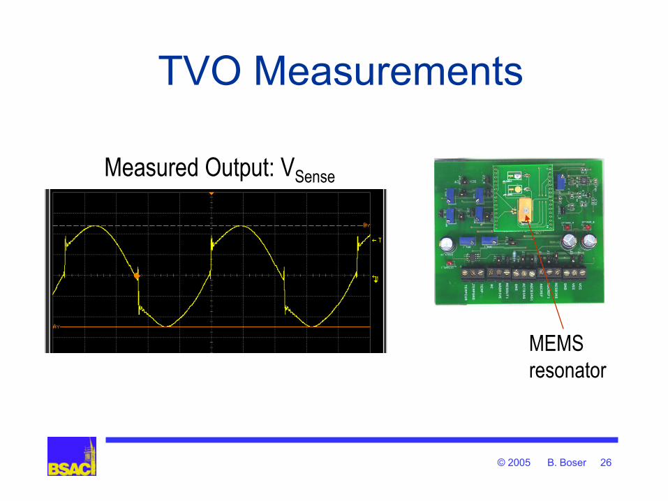
TVO Measurements
MEMS
resonator
Measured Output: VSense

© 2005 B. Boser 27
Measured TVO Phase Noise
• Resolution
– 20-n in 10kHz
– 200-p/rt-Hz
– 40-fm/rt-Hz
• Test equipment:
Agilent 5501A
-130
-120
-110
-100
-90
-80
-70
-60
-50
-40
1 10 100 1000 10000 100000
dBc/
Hz
offset from carrier, f [Hz]
© 2005 B. Boser 28
MEMS Oscillator Noise
Roessig
1997
Nguyen
1999
Seshia
2002
Seth
2004
This Work
2004
Noise Lfar [dBc/Hz] -70 -70 -75 -83 -120
Vacuum
Monolithic
Frequency, fo 175 kHz 16.5 kHz 145 kHz 57 kHz 217 kHz
Motional Res., Rx ? 3.8 M ? 2.5 M 18 M
Q 17000 51000 10000 14000 370
Amplitude VDrive ? ~ 34 mV ~36 mV 5.3 mV 10 V
© 2005 B. Boser 29
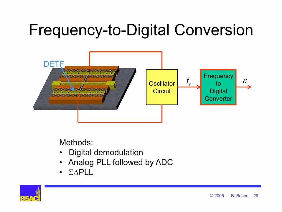
Frequency-to-Digital Conversion
Oscillator
Circuit
Frequency
to
Digital
Converter
f
DETF
Methods:
• Digital demodulation
• Analog PLL followed by ADC
• SPLL
© 2005 B. Boser 30
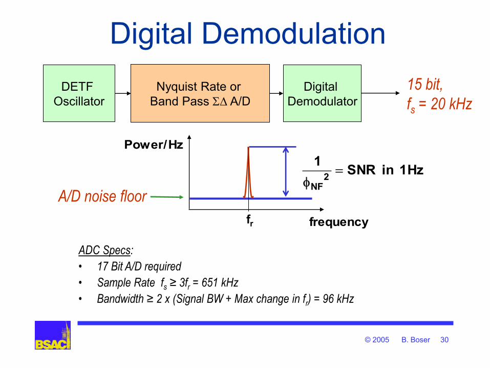
Digital Demodulation
Nyquist Rate or
Band Pass S A/D
Digital
Demodulator
15 bit,
fs = 20 kHz DETF
Oscillator
1Hz inSNR 1
2NF
rf frequency
Hz/Power
A/D noise floor
ADC Specs:
• 17 Bit A/D required
• Sample Rate fs ≥ 3fr = 651 kHz
• Bandwidth ≥ 2 x (Signal BW + Max change in fr) = 96 kHz
© 2005 B. Boser 31
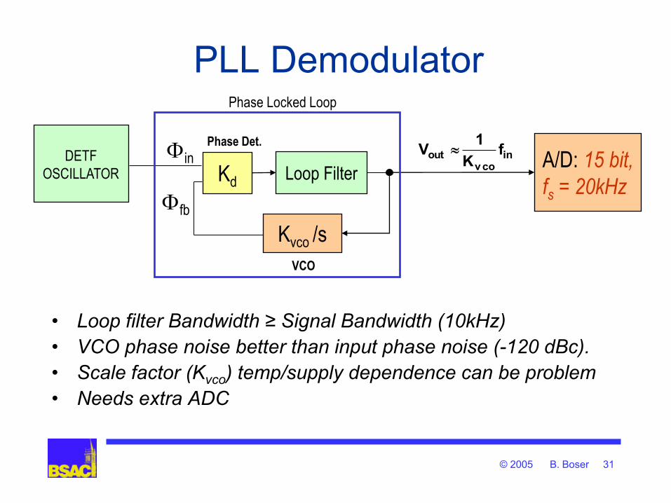
PLL Demodulator
• Loop filter Bandwidth ≥ Signal Bandwidth (10kHz)
• VCO phase noise better than input phase noise (-120 dBc).
• Scale factor (Kvco) temp/supply dependence can be problem
• Needs extra ADC
DETF
OSCILLATOR
Kvco /s
Loop Filter
Fin
Ffb
VCO
Phase Det.
Kd
A/D: 15 bit,
fs = 20kHz
Phase Locked Loop
inv co
out fK
1V
© 2005 B. Boser 32
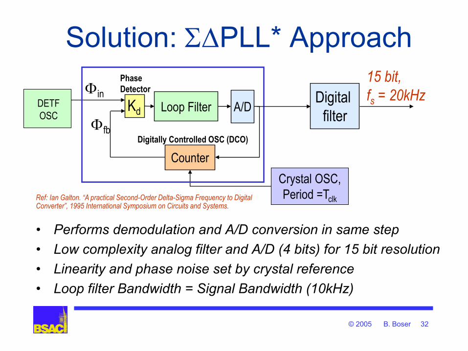
Solution: SPLL* Approach
• Performs demodulation and A/D conversion in same step
• Low complexity analog filter and A/D (4 bits) for 15 bit resolution
• Linearity and phase noise set by crystal reference
• Loop filter Bandwidth = Signal Bandwidth (10kHz)
Phase
Detector Digital
filter
Ref: Ian Galton. “A practical Second-Order Delta-Sigma Frequency to Digital Converter”, 1995 International Symposium on Circuits and Systems.
15 bit,
fs = 20kHz A/D
Counter
Kd
Crystal OSC,
Period =Tclk
DETF
OSC
Digitally Controlled OSC (DCO)
Fin
Ffb
Loop Filter
© 2005 B. Boser 33
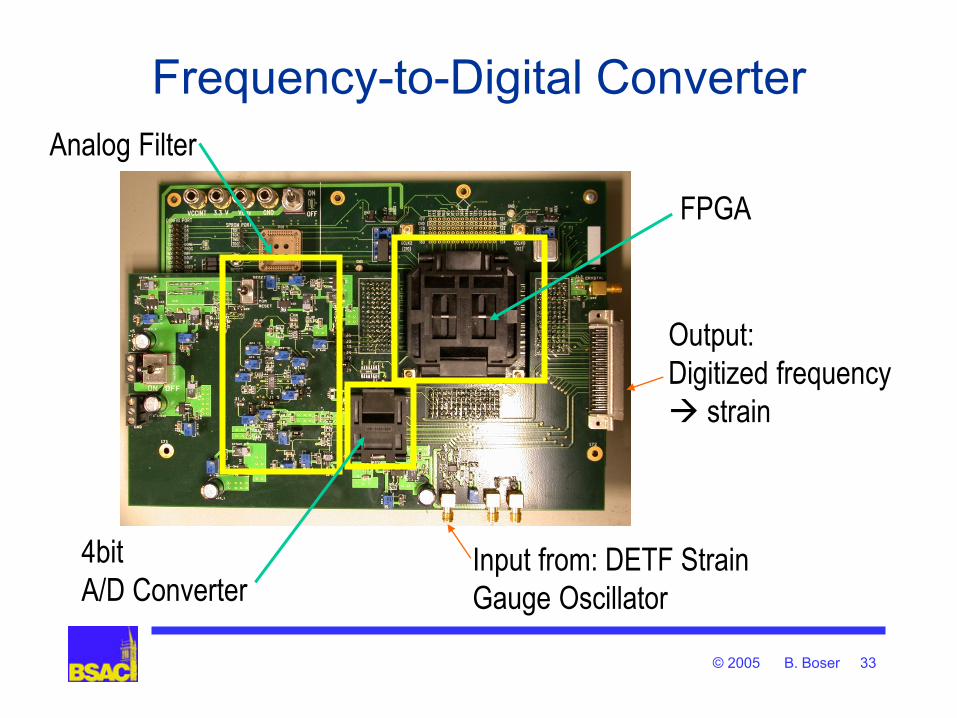
Frequency-to-Digital Converter
Output:
Digitized frequency
strain
Input from: DETF Strain
Gauge Oscillator
Analog Filter
4bit
A/D Converter
FPGA

© 2005 B. Boser 34
101
102
103
104
105
10-8
10-6
10-4
10-2
100
102
Strain Resolution
Bandwidth (Hz)
mic
ro-s
train
number of points: 216
Simulated w/ 2% PFD mismatch and oscillator noise (red)resolution: 0.0294 microstrain
Measured (black) resolution: 0.0334 microstrain
Simulated 2% PFD mismatch and no oscillator noise (green) resolution: 0.027 microstrain
Measured Strain Resolution
mic
ro-s
trai
n, m
/rt
-Hz
Bandwidth (Hz)

© 2005 B. Boser 35
Test with Strain Actuator
Strain Actuator 10
1 10
2 10
3 10
4 10
5
10 -5
10 -4
10 -3
10 -2
10 -1
10 0
10 1
10 2 Strain Resolution
Bandwidth (Hz)
mic
ro-s
train
m
icro
-str
ain
Bandwidth [Hz]
DETF
100Hz
300Hz
1kHz 10kHz strain input
© 2005 B. Boser 36
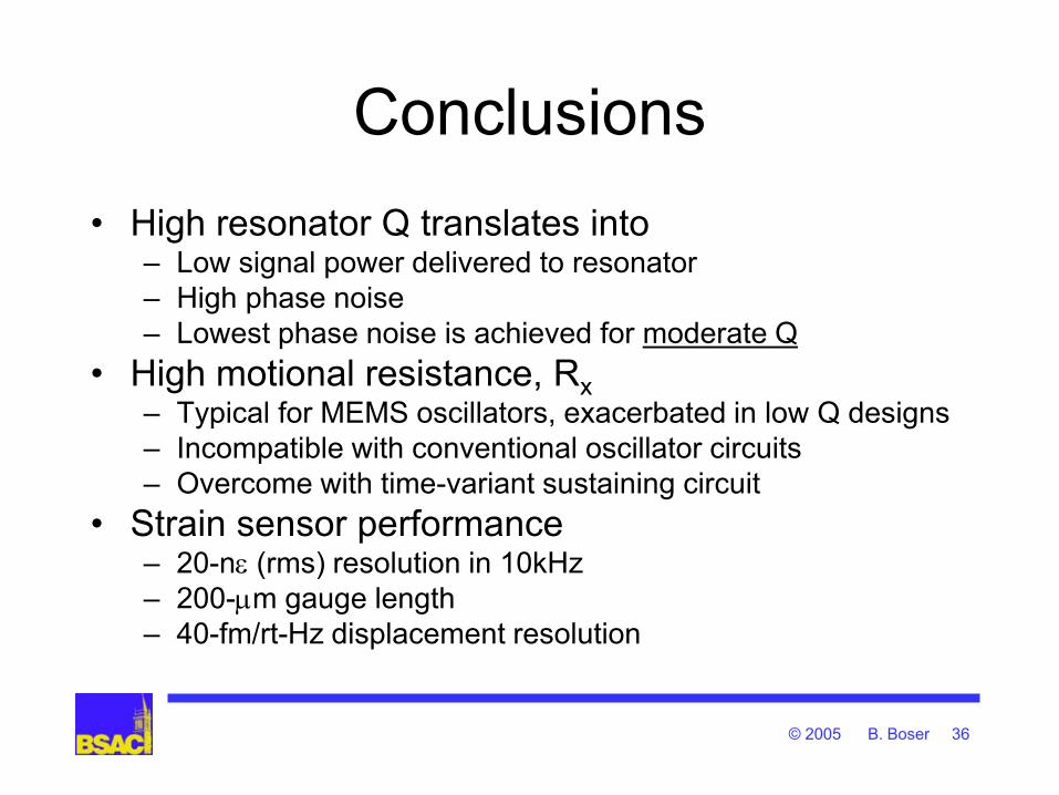
Conclusions
• High resonator Q translates into – Low signal power delivered to resonator
– High phase noise
– Lowest phase noise is achieved for moderate Q
• High motional resistance, Rx – Typical for MEMS oscillators, exacerbated in low Q designs
– Incompatible with conventional oscillator circuits
– Overcome with time-variant sustaining circuit
• Strain sensor performance – 20-n (rms) resolution in 10kHz
– 200-mm gauge length
– 40-fm/rt-Hz displacement resolution

© 2005 B. Boser 37
Acknowledgements
• BSAC strain sensor research team under
Professor Albert Pisano
• Wayne Denny and Graham Mcdearmon of
Timken Company
• Bosch RTC for help with testing
• Bosch for fabrication
• Vladimir Petkov, Baris Cagdaser, Manu Seth
• Army Research Office grant # 19-02-1-0198