resistive products power dissipation in high precision … · power dissipation in high precision...
TRANSCRIPT
Document Number: 53048 www.vishay.comRevision: 29-Oct-09 1
V I S H AY S FE R N I C E
Resistive Products Application Note
Power Dissipation in High Precision Vishay Sfernice Chip Resistors and Arrays (P Thin Film, PRA Arrays, CHP Thick Film)
AP
PL
ICA
TIO
N N
OT
E
A. ABSTRACTDatasheets for surface-mount components in general and for chip resistors and arrays in particular tend to offer very limitedinformation on thermal performance. Typically they provide derating curves that are similar to the ones used for through-holecomponents, even though the respective heat dissipation properties of these two component types are quite different. In thelarger, leaded components, heat dissipation occurs mainly by direct convection and radiation from the component tothe ambient. Only a small portion of the heat is dissipated by conduction through the leads and PCB and then by convection andradiation to the ambient. Thus it makes sense to take the component body temperature as a basis for determining by how muchthe power needs to be derated when this temperature increases. In smaller surface-mount components such as Vishay’s thinfilm chip resistors and arrays, by contrast, more than 90 % of the heat, is dissipated from the body of the component directly intothe solder pad, from there to the PCB, and thence by convection to the ambient.Unfortunately the only specifications on the datasheet that are key to the thermal management process are themaximum junction temperature and internal thermal resistance. Everything else depends on the system design, including theambient temperature, cooling system, thermal behavior of the PCBs, maximum temperature of the solder joints, and so forth.This application note provides designers with addtional guidance on how to get the best performance from high-precision thinfilm chip resistors and arrays from a thermal management point of view.
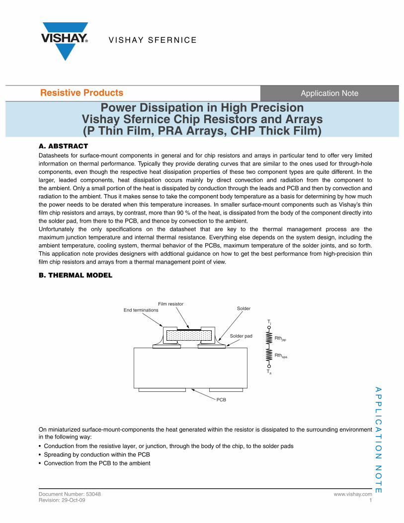
B. THERMAL MODEL
On miniaturized surface-mount-components the heat generated within the resistor is dissipated to the surrounding environmentin the following way:
• Conduction from the resistive layer, or junction, through the body of the chip, to the solder pads
• Spreading by conduction within the PCB• Convection from the PCB to the ambient
End terminationsFilm resistor
Solder
Solder pad
PCB
Tj
Rthjsp
Rthspa
Ta
Power Dissipation in High Precision Vishay Sfernice Chip Resistors and Arrays (P Thin Film, PRA Arrays, CHP Thick Film)
www.vishay.com Document Number: 530482 Revision: 29-Oct-09
Application NoteVishay Sfernice
AP
PL
ICA
TIO
N N
OT
E
The components are so small compared to the PCB that heat removal by direct convection and/or radiation from the resistor bodyis ignored in the following simple but well recognized model:
1. Tj = Ta + Rthja x Pd = Ta + (Rthjsp + Rthspa) x Pd = Ta + Rthjsp x Pd + Rthspa x Pd
2. Tsp = Ta + Rthspa x Pd
where
• Tj is the temperature of the resistive layer, or junction
• Ta is the ambient temperature around the PCB
• Tsp is the temperature of the solder pad, underneath the solder joint, it is almost equal to solder joint temperature
• Pd is the power dissipation of the resistor
• Rthja is the thermal resistance between the resistive layer and the ambient
• Rthjsp is the thermal resistance between the resistive layer and the solder joint
• Rthspa is the thermal resistance between the solder joint and the ambient
• Rthspa takes into account the conduction within the PCB and the convection from the PCB to the ambient
The key thermal resistance value for component manufacturers is Rthjsp, which is affected by the choice of material, the resistorpattern, and the terminations. Manufacturers also strive to improve the thermal stability of their resistors, such that the devicescan withstand higher and higher temperatures without undergoing significant drifts, and the maximum junction temperature canbe increased. All the other thermal parameters must be addressed by the system designer, who must take into consideration thePCB material, the thickness and the layout of the copper tracks, the cooling system, the interaction between surroundingcomponents, and so forth.
With increasing use of computer-aided design, this is the only way to handle the more and more stringent requirements imposedby miniaturization, higher power density, temperature exposure, reliability, and so forth.Indeed, there are severe consequences for inadequate thermal management, including melting or unreliability of the solder joints,impaired PCB performance, and impaired resistor performance being caused by too much drift, either reversible or irreversible.
This is why thermal management is so important.
C. DATAAs noted previously, the nominal power and derating information supplied by datasheets is inadequate to allow designers to getthe best performance from chip resistors, and sometimes it can even be misleading. This application note provides designers withthe Rthjsp for standard and enlarged-termination parts as well as experimental data relevant to chip resistors of standard sizesmounted on various PCB types to allow them to use the thermal model presented above. These PCBs have been chosen to berepresentative of the worst, typical, and best cases in terms of thermal resistance. The resulting data will help designers who cannot calculate thermal resistance by themselves, or to complete their CAD approach.
The Rthjsp values were computed from datasheet information and the following thermal conductivity values:
Table 1 contains all the data necessary to make calculations using the thermal model.
MATERIAL THERMAL CONDUCTIVITY (W x m-1 x K-1)
Alumina 25
Cu 400
Ni and SnAg 50
FR4 0.26
AIN 100 up to 200
Power Dissipation in High Precision Vishay Sfernice Chip Resistors and Arrays (P Thin Film, PRA Arrays, CHP Thick Film)
Application NoteVishay Sfernice
Document Number: 53048 www.vishay.comRevision: 29-Oct-09 3
AP
PL
ICA
TIO
N N
OT
E
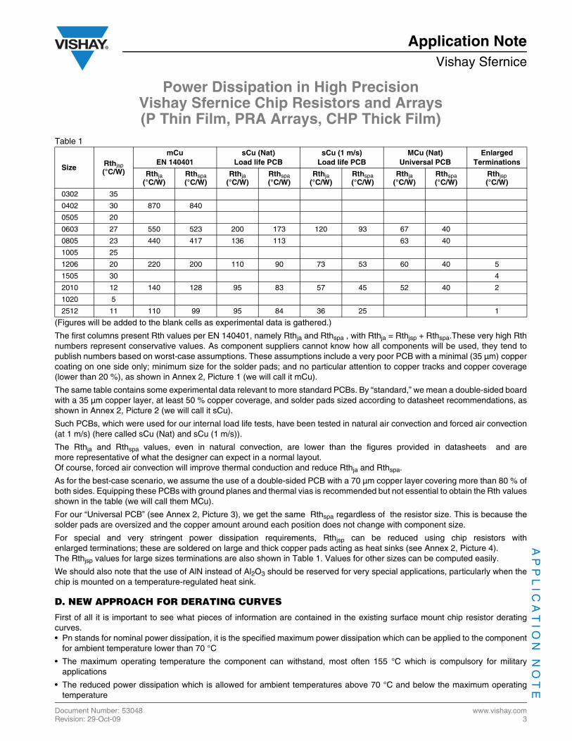
Table 1
(Figures will be added to the blank cells as experimental data is gathered.)
The first columns present Rth values per EN 140401, namely Rthja and Rthspa , with Rthja = Rthjsp + Rthspa.These very high Rthnumbers represent conservative values. As component suppliers cannot know how all components will be used, they tend topublish numbers based on worst-case assumptions. These assumptions include a very poor PCB with a minimal (35 µm) coppercoating on one side only; minimum size for the solder pads; and no particular attention to copper tracks and copper coverage(lower than 20 %), as shown in Annex 2, Picture 1 (we will call it mCu).
The same table contains some experimental data relevant to more standard PCBs. By “standard,” we mean a double-sided boardwith a 35 µm copper layer, at least 50 % copper coverage, and solder pads sized according to datasheet recommendations, asshown in Annex 2, Picture 2 (we will call it sCu).
Such PCBs, which were used for our internal load life tests, have been tested in natural air convection and forced air convection(at 1 m/s) (here called sCu (Nat) and sCu (1 m/s)).
The Rthja and Rthspa values, even in natural convection, are lower than the figures provided in datasheets and aremore representative of what the designer can expect in a normal layout. Of course, forced air convection will improve thermal conduction and reduce Rthja and Rthspa.
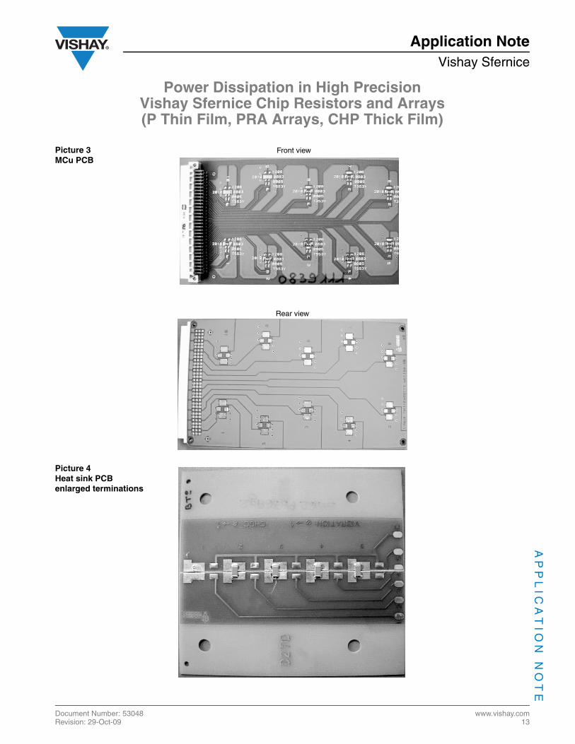
As for the best-case scenario, we assume the use of a double-sided PCB with a 70 µm copper layer covering more than 80 % ofboth sides. Equipping these PCBs with ground planes and thermal vias is recommended but not essential to obtain the Rth valuesshown in the table (we will call them MCu).
For our “Universal PCB” (see Annex 2, Picture 3), we get the same Rthspa regardless of the resistor size. This is because thesolder pads are oversized and the copper amount around each position does not change with component size.
For special and very stringent power dissipation requirements, Rthjsp can be reduced using chip resistors withenlarged terminations; these are soldered on large and thick copper pads acting as heat sinks (see Annex 2, Picture 4). The Rthjsp values for large sizes terminations are also shown in Table 1. Values for other sizes can be computed easily.
We should also note that the use of AlN instead of Al2O3 should be reserved for very special applications, particularly when thechip is mounted on a temperature-regulated heat sink.
D. NEW APPROACH FOR DERATING CURVES
First of all it is important to see what pieces of information are contained in the existing surface mount chip resistor deratingcurves.• Pn stands for nominal power dissipation, it is the specified maximum power dissipation which can be applied to the component
for ambient temperature lower than 70 °C
• The maximum operating temperature the component can withstand, most often 155 °C which is compulsory for militaryapplications
• The reduced power dissipation which is allowed for ambient temperatures above 70 °C and below the maximum operatingtemperature
Size Rthjsp(°C/W)
mCuEN 140401
sCu (Nat)Load life PCB
sCu (1 m/s)Load life PCB
MCu (Nat)Universal PCB
EnlargedTerminations
Rthja(°C/W)
Rthspa(°C/W)
Rthja(°C/W)
Rthspa(°C/W)
Rthja(°C/W)
Rthspa(°C/W)
Rthja(°C/W)
Rthspa(°C/W)
Rthjsp(°C/W)
0302 35
0402 30 870 840
0505 20
0603 27 550 523 200 173 120 93 67 40
0805 23 440 417 136 113 63 40
1005 25
1206 20 220 200 110 90 73 53 60 40 5
1505 30 4
2010 12 140 128 95 83 57 45 52 40 2
1020 5
2512 11 110 99 95 84 36 25 1
Power Dissipation in High Precision Vishay Sfernice Chip Resistors and Arrays (P Thin Film, PRA Arrays, CHP Thick Film)
www.vishay.com Document Number: 530484 Revision: 29-Oct-09
Application NoteVishay Sfernice
AP
PL
ICA
TIO
N N
OT
E
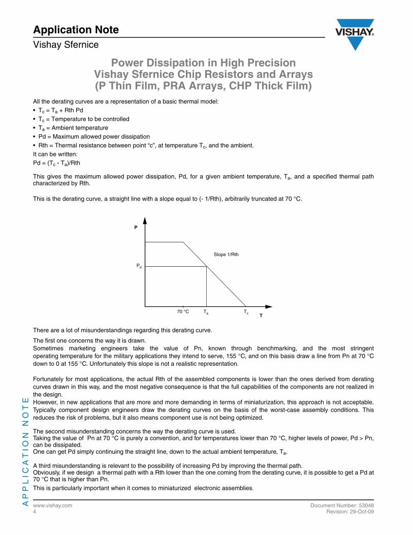
All the derating curves are a representation of a basic thermal model:• Tc = Ta + Rth Pd
• Tc = Temperature to be controlled
• Ta = Ambient temperature• Pd = Maximum allowed power dissipation
• Rth = Thermal resistance between point “c”, at temperature Tc, and the ambient.
It can be written:Pd = (Tc - Ta)/Rth
This gives the maximum allowed power dissipation, Pd, for a given ambient temperature, Ta, and a specified thermal pathcharacterized by Rth.
This is the derating curve, a straight line with a slope equal to (- 1/Rth), arbitrarily truncated at 70 °C.
There are a lot of misunderstandings regarding this derating curve.
The first one concerns the way it is drawn.Sometimes marketing engineers take the value of Pn, known through benchmarking, and the most stringentoperating temperature for the military applications they intend to serve, 155 °C, and on this basis draw a line from Pn at 70 °Cdown to 0 at 155 °C. Unfortunately this slope is not a realistic representation.
Fortunately for most applications, the actual Rth of the assembled components is lower than the ones derived from deratingcurves drawn in this way, and the most negative consequence is that the full capabilities of the components are not realized inthe design.However, in new applications that are more and more demanding in terms of miniaturization, this approach is not acceptable.Typically component design engineers draw the derating curves on the basis of the worst-case assembly conditions. Thisreduces the risk of problems, but it also means component use is not being optimized.
The second misunderstanding concerns the way the derating curve is used.Taking the value of Pn at 70 °C is purely a convention, and for temperatures lower than 70 °C, higher levels of power, Pd > Pn,can be dissipated.One can get Pd simply continuing the straight line, down to the actual ambient temperature, Ta.
A third misunderstanding is relevant to the possibility of increasing Pd by improving the thermal path.Obviously, if we design a thermal path with a Rth lower than the one coming from the derating curve, it is possible to get a Pd at70 °C that is higher than Pn.
This is particularly important when it comes to miniaturized electronic assemblies.
70 °C Ta Tc T
P
Pd
Slope 1/Rth
Power Dissipation in High Precision Vishay Sfernice Chip Resistors and Arrays (P Thin Film, PRA Arrays, CHP Thick Film)
Application NoteVishay Sfernice
Document Number: 53048 www.vishay.comRevision: 29-Oct-09 5
AP
PL
ICA
TIO
N N
OT
E
E. UNDERSTANDING THERMAL PATHSPCB designers working with thermal simulation software can start working with their own data. Such simulations can provide avalue for Rthspa, which will allow the designer to control the temperature of the solder pad, which is also the temperature of thesolder joint.(3) Tsp = Ta + Rthspa x PdAs we’ll see, Tsp is the most important temperature parameter to get under control.
With SnPb solder alloys and FR4 board material, the maximum recommended Tsp is 110 °C.For SnAg solder alloys and special PCBs, this maximum temperature can potentially be increased, up to 150 °C, but there isinsufficient data on SnAg solder joints to make this a general rule. What we do know is that the higher the Ta, the less power canbe applied. Thus for a given Ta < Tsp max. one can find the allowed power dissipation by:(4) P = (Tsp max. - Ta)/Rthspa
This is the equation of the derating curve relevant to the solder pad.
To obtain the best performance from chip resistors, Tj should also be kept lower than 155 °C.
This is the maximum temperature specified on Vishay datasheets, although for high- temperature applications specially treateddevices are available that increase Tj max. up to 200 °C and even higher.(5) Tj = Ta + Rthjsp x Pd + Rthspa x PdFor a given Ta < Tj max. one can get the allowed power dissipation(6) P = (Tj max. - Ta)/(Rthjsp + Rthspa)
This is the equation of the derating curve relevant to the junction or resistive layer.
The signs of overheating of the solder pads or/and of the PCB material are visible far before any significant drift of the ohmicvalue can be detected, this means that controlling Tsp is a priority.This also confirms what the thermal model is showing. For the combinations of Pd and Rthjsp that we are dealing with,the thermal gradient between the junction and the solder pad is lower than 20 °C, as Vishay resistors are designed towork optimally at junction temperatures up to 175 °C; thus there is no limitation imposed by Tj.
We will be issuing a special datasheet dedicated to 200 °C applications. Thus, for applications other than 200 °C ones, requiringspecial assemblies, we will focus on the limitation imposed by Tsp max.
For the different chip sizes, we can draw up derating curves from equation (4) taking into account figures from Table 1 and thethree typical PCB configurations already discussed, mCu, sCu, and MCu.
This set of curves, (or simple calculations obtained by a worksheet from the basic thermal model) might be helpful for PCBdesigners not equipped to perform the analyses necessary for accurate thermal management .
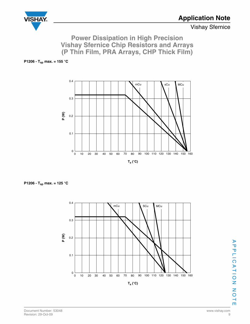
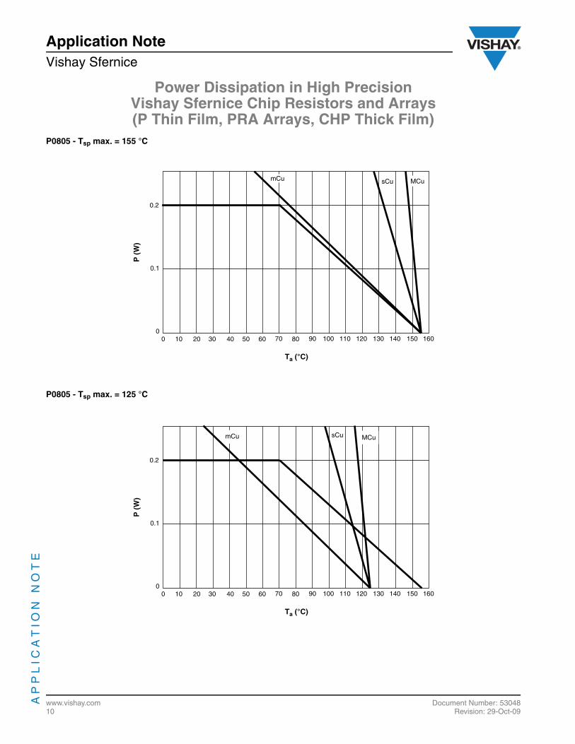
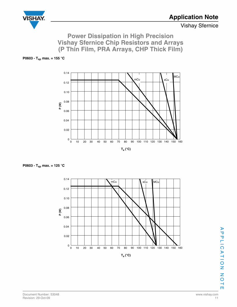
Let’s consider the respective consequences when Tsp max. = 155 °C (equal to Tj max.) and Tsp max. = 125 °C.
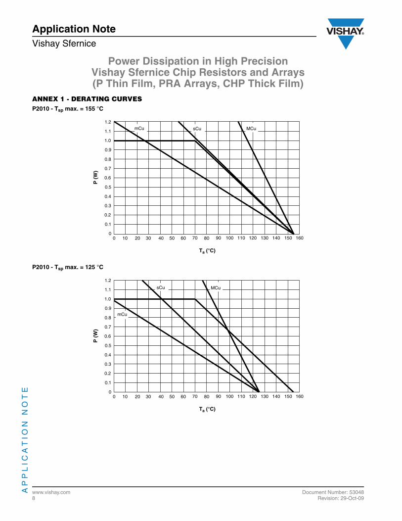
E.1 Tsp max. = 155 °CFor military applications, the assembly and the solder joint can withstand 155 °C, which is the maximum operating temperature.We have provided curves relevant to the most standard sizes (0603, 0805,1206, and 2010) and additional curves can be createdfrom the derating curve equations (4) and (6).On the graph shown in Annex 1 we can see :
• The datasheet derating curve
• The derating curves relevant to Tsp for “mCu”, “sCu”, and “MCu”
The equations and the corresponding curves allow some interesting observations.
• For 0603, 0805, and 1206 sizes, and even for the worst-case “mCu” PCB, the “Tsp derating curves” are above those providedon the datasheets; this means that one can apply a higher Pd than specified in the datasheet. In fact the Pd at 70 °C can be increased respectively up to 162 mW, 203 mW, and 425 mW
• For the 2010 size, an “sCu” should be used in order to achieve a Tsp < 155 °C under 1 W. If one has to assemble a P2010 onan “mCu” PCB, the Pd at 70 °C should be reduced down to 0.66 W.
Using an “MCu” PCB, the applied power can be very high compared to Pn.
Power Dissipation in High Precision Vishay Sfernice Chip Resistors and Arrays (P Thin Film, PRA Arrays, CHP Thick Film)
www.vishay.com Document Number: 530486 Revision: 29-Oct-09
Application NoteVishay Sfernice
AP
PL
ICA
TIO
N N
OT
E
E.2 Tsp max. = 125 °CNumerous applications require components with a maximum operating temperature of 125 °C. The corresponding set of “Tsp = 125 °C derating curves” can be drawn very easily from the previous “Tsp = 155 °C” ones. Justmake a “30 °C” translation .
In this case the remarks are:
• The “Tsp derating curves” relevant to “mCu” are below the datasheet ones, this means that this “Tsp derating curve” is applicableover the others.
• The Pd at 70 °C must be decreased for the 0603, 0805, 1206 and 2010 sizes respectively down to 103 mW, 132 mW and390 mW.
• The “Tsp derating curves” relevant to “sCu” are partly below and, partly above the datasheet values for the 0603, 0805, and1206 sizes.
• The cross-over temperatures are respectively 115 °C, 113 °C, and 110 °C
• Above the cross-over temperature, the “Tsp derating curve” should be used; below this temperature the same curve can alsobe used
• For the 2010 size, the “Tsp derating curves” relevant to “sCu” are applicable for Ta > 42 °C
• The “Tsp derating curves” relevant to “MCu” are partly below, partly above the datasheet ones for sizes 0603, 0805, 1206and 2010
• The cross-over temperatures are respectively 122 °C, 120 °C, and 87 °C
• Above the crossover temperature, the “Tsp derating curve” must be used; below this temperature the same curve can also beused.
Simple translation of these curves will give figures relevant to any value forTsp max.
F. ENLARGED TERMINATIONS FOR LARGEST CHIP SIZE
It is tempting to suppose that the of use larger chips by itself could serve as a solution when more power needs to be dissipated.Calculations and measurements show, this is obviously not the case and a great deal of attention should be paid to the thermalmanagement of the largest chip resistors.One way to optimize real estate is to use enlarged terminations together with a high power dissipating PCB, such as the MCutype.As Table 1 shows the main limitation comes from Rthspa.Therefore the Tsp derating curves are quite easy to draw.Pd = (Tsp - Ta)/(Rthspa + Rthjsp) And the result is a straight line starting from Tsp max., with a slope roughly equal to (- 1/40) W/°C.
G. CONCLUSION
On the basis of a simple but well recognized thermal model we have shown that Tsp, the temperature of the solder pad, is themost important temperature parameter that needs to be controlled in order to get the best performance from chip resistors andarrays.Components designers are working to
• Increase the maximum allowed temperature junction: Tj
• Reduce the internal thermal resistance: Rthjsp
• Improve the thermal stability of the internal layers
As a consequence Tsp is most often the limiting parameter and therefore, the importance of controlling Tsp is more important thanever.
Thermal management through Tsp control is the task of assembly design engineers. To help them in this task we have compiledand provided the experimental data included in this application note.
Power Dissipation in High Precision Vishay Sfernice Chip Resistors and Arrays (P Thin Film, PRA Arrays, CHP Thick Film)
Application NoteVishay Sfernice
Document Number: 53048 www.vishay.comRevision: 29-Oct-09 7
AP
PL
ICA
TIO
N N
OT
E
Highlights from this compilation are:
1. If Tsp max. = 155 °C is acceptable for the solder joint, and for the PCB, integrity and reliability, then:
• Worst case “mCu” PCBs can be used without any power derating in excess of the value indicated by the datasheet, except forP2010 devices (see curve).
• Pd can be slightly higher than Pn at Ta = 70 °C.
• For Ta < 70 °C a higher Pd is acceptable, and can be derived from the Tsp derating curve.
• At a minimum standard “sCu” PCBs should be used with P2010.
• For smaller sizes “sCu” assembly allows a higher Pd than specified.
• “MCu” PCBs allow an even higher Pd.
2. If Tsp max. = 125 °C, the following guidelines should be followed to ensure solder joint reliability:
• For “mCu” PCBs, the Tsp derating curve is applicable
• For “sCu” PCBs, the Tsp derating curve will reduce Pd for Ta > 110 °C and will allow a higher Pd for Ta < 110 °C(for P2010, the Tsp derating curve is applicable)
• For “MCu” PCBs, the Tsp derating curve will reduce Pd for Ta > 120 °C and will allow higher Pd for Ta < 120 °C (for P2010, the Tsp derating curve is applicable)
3. Enlarged terminations chips mounted on “MCu” PCBs allow for better power dissipation, and represent an interesting solutionfor large size chips. The Tsp derating curve, with a Rthspa close to 40 °C/W, is applicable.
Power Dissipation in High Precision Vishay Sfernice Chip Resistors and Arrays (P Thin Film, PRA Arrays, CHP Thick Film)
www.vishay.com Document Number: 530488 Revision: 29-Oct-09
Application NoteVishay Sfernice
AP
PL
ICA
TIO
N N
OT
E
ANNEX 1 - DERATING CURVESP2010 - Tsp max. = 155 °C
P2010 - Tsp max. = 125 °C
0.4
0.3
0.2
0.1
00 10 20 30 40 50 60 70 80 90 100 110 120 130 140 150 160
P (
W)
Ta (°C)
0.8
0.7
0.6
0.5
1.2
1.1
1.0
0.9
MCusCumCu
0.4
0.3
0.2
0.1
00 10 20 30 40 50 60 70 80 90 100 110 120 130 140 150 160
P (
W)
Ta (°C)
0.8
0.7
0.6
0.5
1.2
1.1
1.0
0.9
MCusCu
mCu
Power Dissipation in High Precision Vishay Sfernice Chip Resistors and Arrays (P Thin Film, PRA Arrays, CHP Thick Film)
Application NoteVishay Sfernice
Document Number: 53048 www.vishay.comRevision: 29-Oct-09 9
AP
PL
ICA
TIO
N N
OT
E
P1206 - Tsp max. = 155 °C
P1206 - Tsp max. = 125 °C
0.4
0.3
0.2
0.1
00 10 20 30 40 50 60 70 80 90 100 110 120 130 140 150 160
P (
W)
Ta (°C)
MCusCumCu
0.4
0.3
0.2
0.1
00 10 20 30 40 50 60 70 80 90 100 110 120 130 140 150 160
P (
W)
Ta (°C)
MCuSCumCu
Power Dissipation in High Precision Vishay Sfernice Chip Resistors and Arrays (P Thin Film, PRA Arrays, CHP Thick Film)
www.vishay.com Document Number: 5304810 Revision: 29-Oct-09
Application NoteVishay Sfernice
AP
PL
ICA
TIO
N N
OT
E
P0805 - Tsp max. = 155 °C
P0805 - Tsp max. = 125 °C
0.2
0.1
00 10 20 30 40 50 60 70 80 90 100 110 120 130 140 150 160
P (
W)
Ta (°C)
MCusCumCu
0.2
0.1
00 10 20 30 40 50 60 70 80 90 100 110 120 130 140 150 160
P (
W)
Ta (°C)
MCusCumCu
Power Dissipation in High Precision Vishay Sfernice Chip Resistors and Arrays (P Thin Film, PRA Arrays, CHP Thick Film)
Application NoteVishay Sfernice
Document Number: 53048 www.vishay.comRevision: 29-Oct-09 11
AP
PL
ICA
TIO
N N
OT
E
P0603 - Tsp max. = 155 °C
P0603 - Tsp max. = 125 °C
0.08
0.06
0.04
0.02
00 10 20 30 40 50 60 70 80 90 100 110 120 130 140 150 160
P (
W)
Ta (°C)
0.14
0.12
0.10
MCusCumCu
0.08
0.06
0.04
0.02
00 10 20 30 40 50 60 70 80 90 100 110 120 130 140 150 160
P (
W)
Ta (°C)
0.14
0.12
0.10
MCusCumCu
Power Dissipation in High Precision Vishay Sfernice Chip Resistors and Arrays (P Thin Film, PRA Arrays, CHP Thick Film)
www.vishay.com Document Number: 5304812 Revision: 29-Oct-09
Application NoteVishay Sfernice
AP
PL
ICA
TIO
N N
OT
E
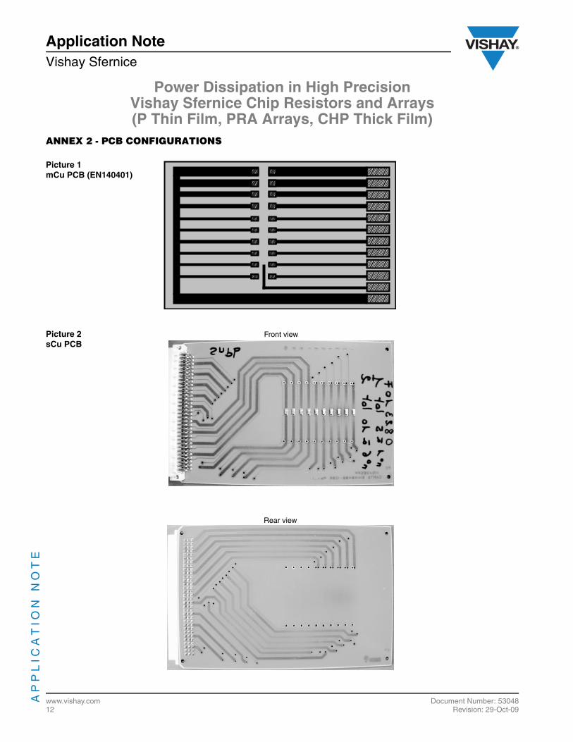
ANNEX 2 - PCB CONFIGURATIONS
Picture 1mCu PCB (EN140401)
Picture 2sCu PCB
Front view
Rear view
Power Dissipation in High Precision Vishay Sfernice Chip Resistors and Arrays (P Thin Film, PRA Arrays, CHP Thick Film)
Application NoteVishay Sfernice
Document Number: 53048 www.vishay.comRevision: 29-Oct-09 13
AP
PL
ICA
TIO
N N
OT
E
Picture 3MCu PCB
Front view
Rear view
Picture 4Heat sink PCB enlarged terminations