renice x2 2.5 sata ssd(rev.1.4) - neoboxpc, minipc …€¦ · form factor with sata interface....
TRANSCRIPT

2011
Shi Jian Lee
Renice Technology Co., Limited
2011-12-25
RENICE X2 2.5" SATA SSD(Rev.1.4)
DATA SHEET
Renice Technology Co., Limited
1
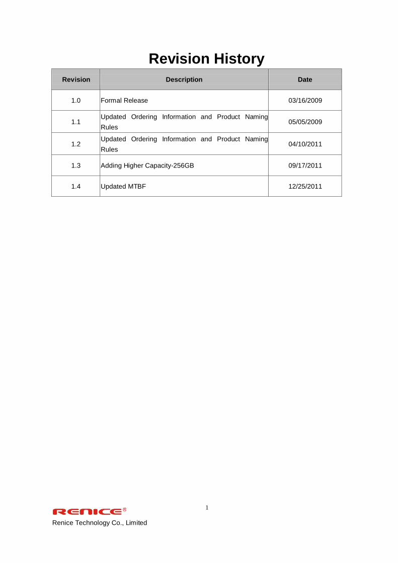
Revision History
Revision Description Date
1.0 Formal Release 03/16/2009
1.1 Updated Ordering Information and Product Naming
Rules 05/05/2009
1.2 Updated Ordering Information and Product Naming
Rules 04/10/2011
1.3 Adding Higher Capacity-256GB 09/17/2011
1.4 Updated MTBF 12/25/2011

Renice Technology Co., Limited
2
CATALOGUE
1. Introduction ...................................................................................................3
1.1 Product Overview.....................................................................................................................3
1.2 Feature .....................................................................................................................................3
2. Functional Block Diagram..........................................................................4
3. Product Specifications ...............................................................................5
3.1 Physical Specifications ...............................................................................................................5
3.2 Host Interface..............................................................................................................................6
3.3 Internal MROM for Boot-loader..................................................................................................6
3.4 H/W Acceleration Engine ...........................................................................................................6
3.5 Mobile SDRAM Interface............................................................................................................6
3.6 Capacity Specification ................................................................................................................6
4. Interface Description ...................................................................................7
4.1 Pin Assignment ...........................................................................................................................7
4.2 Pin Description ............................................................................................................................7
5. Power Specifications ..................................................................................8
5.1 Operating Voltage .......................................................................................................................8
5.2 Power Supply Voltage ................................................................................................................8
5.3 Power Consumption (typical) .....................................................................................................8
6. Reliability Specification ..............................................................................9
6.1 Environment ................................................................................................................................9
6.2 Wear-leveling ..............................................................................................................................9
6.3 Endurance ...................................................................................................................................9
6.4 H/W ECC and EDC for NAND Flash .........................................................................................9
6.5 MTBF ...........................................................................................................................................9
7. Supported ATA Command Lists ............................................................. 10
8. SMART .......................................................................................................... 15
8.1 SMART Command Set .............................................................................................................15
8.2 SMART Attribute Data Structure..............................................................................................16
9. Ordering Information ................................................................................. 17
10. Part Number Naming Rule ..................................................................... 18

Renice Technology Co., Limited
3
1. Introduction
1.1 Product Overview
RENICE X2 2.5” SATA SSD are high-capacity flash memory-based Solid State Drive (SSD) that
electrically comply with Serial ATA (SATA) standard. RENICE X2 2.5” SATA SSD supports SATA II
standard (3.0 Gb/sec) performance. Sustained read speed is up to 250 MB per second, and sustain
write speed is up to 200 MB per second. RENICE X2 2.5” SATA SSD is designed on the 2.5-inch
form factor with SATA interface. RENICE X2 2.5” SATA SSD is designed for industrial field. It
substantially reduces the boot time of an operating system while consuming far less power than a
hard disk drive (HDD). RENICE X2 2.5” SATA SSD are designed to withstand harsh environments.
The SSD is vibration resistant and can work in lower or higher temperature than a standard HDD.
RENICE X2 2.5” SATA SSD complies with ATA protocol, no additional drivers are required, and the
SSD can be configured as a boot device or data storage device.
1.2 Feature
● Standard Serial ATA 2.6: SATA II, 3.0 Gbps
● Form factor: 2.5 inch (100.2mmX69.5mmX9.6mm) L×W×H
● Connector: 7-pin signal segment and a 15-pin power segment
● Performance:
– Burst Rate: 300MB/S
– Sequential Data Read/Write: 250/200MB/s
– 4kb Random Read/Write IOPS: up to 8,000/6,000
– Access Time: 0.1ms
● Capacities: 8GB, 16GB, 32GB, 64GB, 128GB, 256GB
● Nand flash type: SLC or MLC NAND flash
● Input voltage: 5.0V (±5%)
● Temperature ranges:
– Operation:
Industrial: -40 to 85°C (-40° ~ 185°F)
– Storage: -50 to 95°C (-50° ~ 203°F)
● Intelligent features:
– Flash management algorithm: static and dynamic wear-leveling, bad block management algorithm
– Supports dynamic power management and SMART (Self-Monitoring, Analysis and Reporting
Technology)
– High and Reliable ECC capability up to 16bits/sector
– TRIM
● RoHS compliant
● MTBF:>4,000,000 Hours @40C (Tested with Telcordia SR-332 standard)

Renice Technology Co., Limited
4
2. Functional Block Diagram
Figure 1: Renice X2 2.5" SATA SSD Block Diagram

Renice Technology Co., Limited
5
3. Product Specifications
3.1 Physical Specifications
Table 1 Physical Specifications
Figure 2: Renice X2 2.5" SATA SSD mechanical dimensions
Form Factor 2.5 INCH
Dimensions
Length 100.2mm
Width 69.5mm
Height 9.6mm
Weight <76g
Connector SATA II 7+15 pin

Renice Technology Co., Limited
6
3.2 Host Interface
Fully compliant with SATA revision 2.6, compatible with SATA 1.5Gb/s and 3.0Gb/s interface rates
Fully compliant with ATA-7 standard
PIO, DMA, UDMA(up to 6, dependent on host) supported
Native Command Queuing (NCQ): up to 32 commands
S.M.A.R.T. command transport (SCT) technology
3.3 Internal MROM for Boot-loader
Robust Firmware Corruption
Maintenance and diagnostics program in MROM for recovering from drive malfunction
3.4 H/W Acceleration Engine
Internal SRAM and external DRAM search engine
3.5 Mobile SDRAM Interface
60MB buffer memory by Flash capacity
3.6 Capacity Specification
Table 2: Device parameters
Capacity LBA Cylinders Heads Sectors User capacity(MB)
8GB 14442365 16383 16 63 7051.94
16GB 29323728 16383 16 63 14318.23
32GB 62533296 16383 16 63 30533.84
64GB 125045424 16383 16 63 61057.34
128GB 250069680 16383 16 63 122104.3
256GB 500118192 16383 16 63 244193.3

Renice Technology Co., Limited
7
4. Interface Description
4.1 Pin Assignment
Figure 3: Pin Assignments
4.2 Pin Description
Table 3: Signal and Power segment
Pin No. Pin Name Pin No. Pin Name
S1 GND P1 +3.3V(Unused)
S2 SATA Differential RX+ based on SSD P2 +3.3V(Unused)
S3 SATA Differential RX- based on SSD P3 +3.3V(Unused)
S4 GND P4 GND
S5 SATA Differential TX- based on SSD P5 GND
S6 SATA Differential TX+ based on SSD P6 GND
S7 GND P7 5V
P8 5V
P9 5V
P10 GND
P11 DAS/DSS
P12 GND
P13 +12V(Unused)
P14 +12V(Unused)
P15 +12V(Unused)

Renice Technology Co., Limited
8
5. Power Specifications
5.1 Operating Voltage
Operating voltage: 5V (±5%)
5.2 Power Supply Voltage
1.0V for Core, 3.3V for NAND, 1.8V for SDRAM
5.3 Power Consumption (typical)
Operation (Read/Write) – 1.0W
Idle – 0.4W
Standby - 0.4W
Sleep (Partial/Slumber) - 0.4W/0.15W
Renice Technology Co., Limited
9
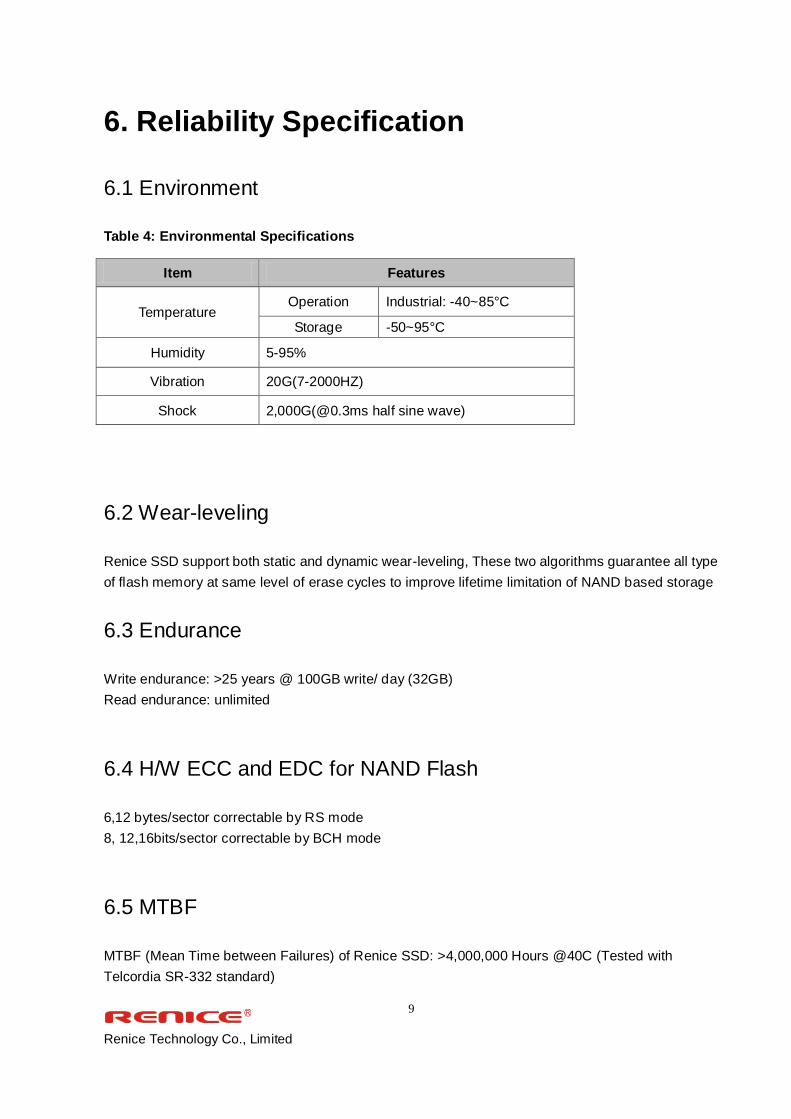
6. Reliability Specification
6.1 Environment
Table 4: Environmental Specifications
6.2 Wear-leveling
Renice SSD support both static and dynamic wear-leveling, These two algorithms guarantee all type
of flash memory at same level of erase cycles to improve lifetime limitation of NAND based storage
6.3 Endurance
Write endurance: >25 years @ 100GB write/ day (32GB)
Read endurance: unlimited
6.4 H/W ECC and EDC for NAND Flash
6,12 bytes/sector correctable by RS mode
8, 12,16bits/sector correctable by BCH mode
6.5 MTBF
MTBF (Mean Time between Failures) of Renice SSD: >4,000,000 Hours @40C (Tested with
Telcordia SR-332 standard)
Item Features
Temperature Operation Industrial: -40~85°C
Storage -50~95°C
Humidity 5-95%
Vibration 20G(7-2000HZ)
Shock 2,000G(@0.3ms half sine wave)

Renice Technology Co., Limited
10
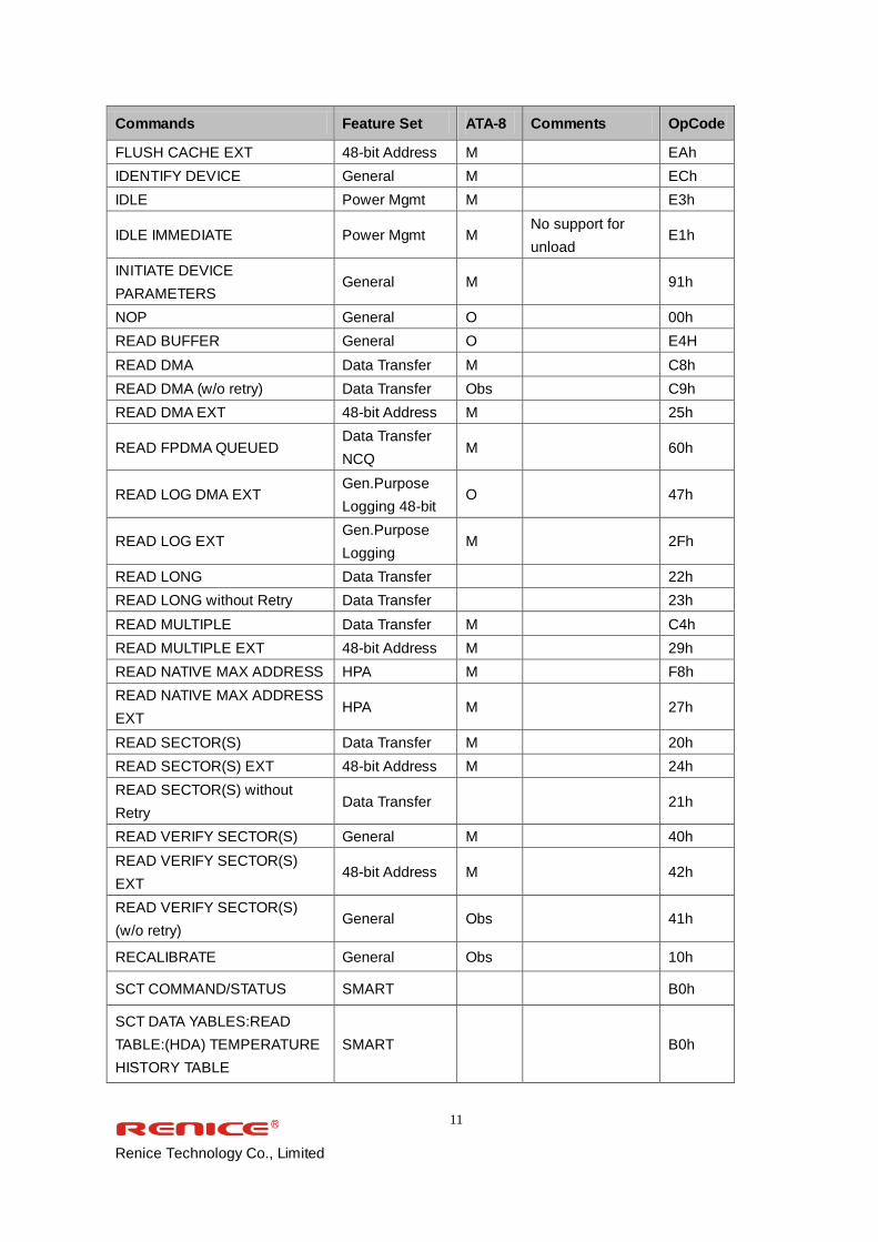
7. Supported ATA Command Lists
Table 5: Support ATA Command Lists
Commands Feature Set ATA-8 Comments OpCode
CHECK POWER MODE Power Mgmt M E5h
DATA SET MANAGEMENT EXT
(I.E.TRIM) Data Set Mgmt O 06h
DISABLE AUTOMATIC
ACOUSTIC MGMT Set Features EFh
DISABLE DEVICE-INITIATED
INTERFACE POWER-STATE
TRANSITIONS
Set Features EFh
DISABLE DMA SETUP FIS
AUTO-ACTIVATE
OPTIMIZATION
Set Features EFh
DISABLE LOOK-AHEAD Set Features EFh
DISABLE REVERTING TO
POWER-ON DEFAULTS Set Features EFh
DISABLE SOFTWARE
SETTINGS PRESERVATION Set Features EFh
DISABLE WRITE CACHE Set Features EFh
DOWNLOAD MICROCODE General O 92h
ENABLE AUTOMATIC
ACOUSTIC MGMT Set Features EFh
ENABLE DEVICE-INITIATED
INTERFACE POWER-STATE
TRANSITIONS
Set Features EFh
ENABLE DMA SETUP FIS
AUTO-ACTIVATE
OPTIMIZATION
Set Features EFh
ENABLE LOOK-AHEAD Set Features EFh
ENABLE REVERTING TO
POWER-ON DEFAULTS Set Features EFh
ENABLE SOFTWARE
SETTINGS PRESERVATION Set Features EFh
ENABLE WRITE CACHE Set Features EFh
EXECUTE DEVICE
DIAGNOSTIC General M 90h
FLUSH CACHE General M E7h
Renice Technology Co., Limited
11
Commands Feature Set ATA-8 Comments OpCode
FLUSH CACHE EXT 48-bit Address M EAh
IDENTIFY DEVICE General M ECh
IDLE Power Mgmt M E3h
IDLE IMMEDIATE Power Mgmt M No support for
unload E1h
INITIATE DEVICE
PARAMETERS General M 91h
NOP General O 00h
READ BUFFER General O E4H
READ DMA Data Transfer M C8h
READ DMA (w/o retry) Data Transfer Obs C9h
READ DMA EXT 48-bit Address M 25h
READ FPDMA QUEUED Data Transfer
NCQ M 60h
READ LOG DMA EXT Gen.Purpose
Logging 48-bit O 47h
READ LOG EXT Gen.Purpose
Logging M 2Fh
READ LONG Data Transfer 22h
READ LONG without Retry Data Transfer 23h
READ MULTIPLE Data Transfer M C4h
READ MULTIPLE EXT 48-bit Address M 29h
READ NATIVE MAX ADDRESS HPA M F8h
READ NATIVE MAX ADDRESS
EXT HPA M 27h
READ SECTOR(S) Data Transfer M 20h
READ SECTOR(S) EXT 48-bit Address M 24h
READ SECTOR(S) without
Retry Data Transfer 21h
READ VERIFY SECTOR(S) General M 40h
READ VERIFY SECTOR(S)
EXT 48-bit Address M 42h
READ VERIFY SECTOR(S)
(w/o retry) General Obs 41h
RECALIBRATE General Obs 10h
SCT COMMAND/STATUS SMART B0h
SCT DATA YABLES:READ
TABLE:(HDA) TEMPERATURE
HISTORY TABLE
SMART B0h

Renice Technology Co., Limited
12
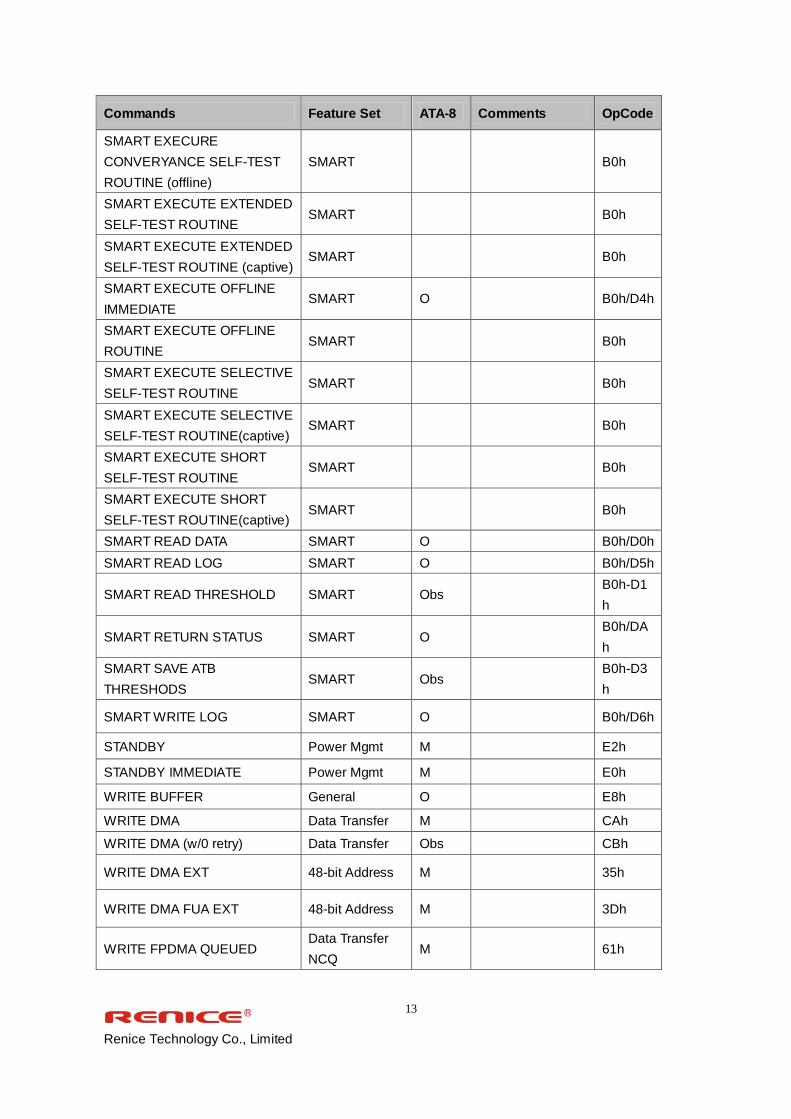
Commands Feature Set ATA-8 Comments OpCode
SCT DATA TRANSFER SMART B0h
SCT FEATURE CONTROL:
FORCED WRITE CACHE
ENABLE & DIABLE
SMART B0h
SCT WRITE SAME SMART
Not recommended
for SSDs:can
negatively affect
initial performance
of drive.
B0h
SECURITY DIABLE
PASSWORD Security M F6h
SECURITY ERASE PREPARE Security M F3h
SECURITY ERASE UNIT Security M F4h
SECURITY FREEZE LOCK Security O F5h
SECURITY SET PASSWORD Security M F1h
SECURITY UNLOCK Security M F2h
SEEK General M 70h
SET MAX ADDRESS HPA M F9h
SET MAX ADDRESS EXT HPA M 37h
SET MAX FREEZE LOCK HPA O F9h/04h
SET MAX LOCK HPA O F9h/02h
SET MAX SET PASSWORD HPA O F9h/01h
SET MAX UNLOCK HPA O F9h/03h
SET MULTIPLE MODE General M C6h
SET TRANSFER MODE(based
on value in SECTOR COUNT
REGISTER
Set Features EFh
SLEEP Power Mgmt M E6h
SMART ABORT OFFLINE
ROUTINE SMART E0h
SMART DISABLE
OPERATIONS SMART M B0h/D9h
SMART ENABLE
OPERATIONS SMART M B0h/D8h
SMART ENABLE/DISABLE
AUTOSAVE SMART M B0h/D2h
SMART EXECUTE
CONVEYANCE SELF-TEST
ROUTINE (captive)
SMART B0h
Renice Technology Co., Limited
13
Commands Feature Set ATA-8 Comments OpCode
SMART EXECURE
CONVERYANCE SELF-TEST
ROUTINE (offline)
SMART B0h
SMART EXECUTE EXTENDED
SELF-TEST ROUTINE SMART B0h
SMART EXECUTE EXTENDED
SELF-TEST ROUTINE (captive) SMART B0h
SMART EXECUTE OFFLINE
IMMEDIATE SMART O B0h/D4h
SMART EXECUTE OFFLINE
ROUTINE SMART B0h
SMART EXECUTE SELECTIVE
SELF-TEST ROUTINE SMART B0h
SMART EXECUTE SELECTIVE
SELF-TEST ROUTINE(captive) SMART B0h
SMART EXECUTE SHORT
SELF-TEST ROUTINE SMART B0h
SMART EXECUTE SHORT
SELF-TEST ROUTINE(captive) SMART B0h
SMART READ DATA SMART O B0h/D0h
SMART READ LOG SMART O B0h/D5h
SMART READ THRESHOLD SMART Obs B0h-D1
h
SMART RETURN STATUS SMART O B0h/DA
h
SMART SAVE ATB
THRESHODS SMART Obs
B0h-D3
h
SMART WRITE LOG SMART O B0h/D6h
STANDBY Power Mgmt M E2h
STANDBY IMMEDIATE Power Mgmt M E0h
WRITE BUFFER General O E8h
WRITE DMA Data Transfer M CAh
WRITE DMA (w/0 retry) Data Transfer Obs CBh
WRITE DMA EXT 48-bit Address M 35h
WRITE DMA FUA EXT 48-bit Address M 3Dh
WRITE FPDMA QUEUED Data Transfer
NCQ M 61h

Renice Technology Co., Limited
14
Commands Feature Set ATA-8 Comments OpCode
WRITE LOG DMA EXT Gen.Purpose
Logging O 57h
WRITE LOG EXT Gen.Purpose
Logging M 3Fh
WRITE LONG Data Transfer 32h
WRITE LONG without Retry Data Transfer 33h
WRITE MULTIPLE Data Transfer M C5h
WRITE MULTIPLE EXT 48-bit Address M 39h
WRITE MULTIPLE FUA EXT 48-bit Address M CEh
WRITE SECTOR(S) Data Transfer M 30h
WRITE SECTOR(S) (w/o retry) Data Transfer Obs 31h
WRITE SECTOR(S) EXT 48-bit Address M 34h
WRITE UNCORRECTABLE
EXT General O 45h
Key:M-Mandatory O-Optional P-Prohibited N-Not defined

Renice Technology Co., Limited
15
8. SMART
8.1 SMART Command Set
Table 6: SMART Command Set
Value(Hex) Command
00-CF Reserved
D0 SMART read attributes
D1﹡ SMART read threshold
D2 SMART enable/disable attribute autosave
D3﹡ SMART save attribute values
D4 SMART execute off-line immediate
D5 SMART read log sector
D6 SMART write log sector
D7﹡ SMART write attribute threshold
D8 SMART enable operations
D9 SMART disable operations
DA SMART return status
DC-FF Reserved(Vendor Specific

Renice Technology Co., Limited
16
8.2 SMART Attribute Data Structure
Table 7: SMART Attribute Data Structure
Byte Description
0:1 SMART structure version number
2 First Stored Attribute Number (i.e."1" for "Raw Read Error Rate")
3:4 Status
5 Nominal value
6 Worst value since SSD was deployed
7:12 Raw Data
13 (Reserved; for some Attributes, the 7th "raw data" byte)
14:25 Next Stored Attribute Number(i.e."3" for "Retired Block Count")
26:361 Next Stored Attribute Nos(max 30 collected Attributes, including above)
362 Off-line data collection status
363 Self-Test execution status byte
364:365 Total time to complete off-line data collection(in seconds)
366 (Reserved)
367 Off-line data collection capability
368:369 SMART capability
370 Error Logging Capability(bit 0 set=device error logging supported)
371 Next Self Test Step
372 Short Self Test routine recommended polling time(in minutes)
373 Extended Self Test routine recommended polling time(in minutes)
374 Recommended polling time for conveyance Self Test
375:376 Time for Extended Self Test if > 255(ie, 373 to FFh)
377:385 (Reserved)
386:510 Vendor information
511 Checksum if data structure (generated on retrieval of stored data)

Renice Technology Co., Limited
17
9. Ordering Information
Table 8: Valid Combinations
Capacity MLC Part Numbers SLC Part Numbers
8GB RIM008-SX22 RIS008-SX22
16GB RIM016-SX22 RIS016-SX22
32GB RIM032-SX22 RIS032-SX22
64GB RIM064-SX22 RIS064-SX22
128GB RIM128-SX22 RIS128-SX22
256GB RIM256-SX22 N
Renice Technology Co., Limited
18
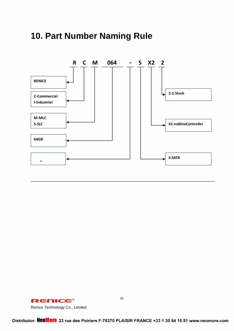
10. Part Number Naming Rule
RENICE
M-MLC
S-SLC
64GB
S-SATA -
C-Commercial
I-Industrial
X2-IndilinxController
2-2.5Inch
R C M 064 - S X2 2