scaled cmos technology reliability users guide - … cmos... · scaled cmos technology reliability...
TRANSCRIPT
National Aeronautics and Space Administration
Scaled CMOS Technology Reliability Users Guide
Mark White Jet Propulsion Laboratory
Pasadena, California
Jet Propulsion Laboratory California Institute of Technology
Pasadena, California
JPL Publication 09-33 01/10

National Aeronautics and Space Administration
Scaled CMOS Technology Reliability Users Guide
NASA Electronic Parts and Packaging (NEPP) Program
Office of Safety and Mission Assurance
Mark White Jet Propulsion Laboratory
Pasadena, California
NASA WBS: 724297.40.43 JPL Project Number: 103982
Task Number: 03.02.02
Jet Propulsion Laboratory 4800 Oak Grove Drive Pasadena, CA 91109
http://nepp.nasa.gov

ii
This research was carried out at the Jet Propulsion Laboratory, California Institute of
Technology, and was sponsored by the National Aeronautics and Space Administration
Electronic Parts and Packaging (NEPP) Program.
Reference herein to any specific commercial product, process, or service by trade name,
trademark, manufacturer, or otherwise, does not constitute or imply its endorsement by
the United States Government or the Jet Propulsion Laboratory, California Institute of
Technology.
Copyright 2010. California Institute of Technology. Government sponsorship
acknowledged.
ii
ABSTRACT
The desire to assess the reliability of emerging scaled microelectronics technologies
through faster reliability trials and more accurate acceleration models is the precursor for
further research and experimentation in this relevant field. The effect of semiconductor
scaling on microelectronics product reliability is an important aspect to the high
reliability application user. From the perspective of a customer or user, who in many
cases must deal with very limited, if any, manufacturer’s reliability data to assess the
product for a highly-reliable application, product-level testing is critical in the
characterization and reliability assessment of advanced nanometer semiconductor scaling
effects on microelectronics reliability. A methodology on how to accomplish this and
techniques for deriving the expected product-level reliability on commercial memory
products are provided.
Competing mechanism theory and the multiple failure mechanism model are applied to
the experimental results of scaled SDRAM products. Accelerated stress testing at
multiple conditions is applied at the product level of several scaled memory products to
assess the performance degradation and product reliability. Acceleration models are
derived for each case. For several scaled SDRAM products, retention time degradation is
studied and two distinct soft error populations are observed with each technology
generation: early breakdown, characterized by randomly distributed weak bits with
Weibull slope β=1, and a main population breakdown with an increasing failure rate.
iii
Retention time soft error rates are calculated and a multiple failure mechanism
acceleration model with parameters is derived for each technology. Defect densities are
calculated and reflect a decreasing trend in the percentage of random defective bits for
each successive product generation.
A normalized soft error failure rate of the memory data retention time in FIT/Gb and
FIT/cm2 for several scaled SDRAM generations is presented revealing a power
relationship. General models describing the soft error rates across scaled product
generations are presented. The analysis methodology may be applied to other scaled
microelectronic products and their key parameters.
iv
Table of Contents List of Tables ..................................................................................................................... vi List of Figures ................................................................................................................... vii Chapter 1: Overview ............................................................................................................1
1.1 Background ............................................................................................................1 1.1.1 Aerospace Vehicle Systems Institute (AVSI) Consortium ....................3 1.1.2 Lifetime Enhancement through Derating ...............................................4 1.1.3 Derating Factor ......................................................................................6 1.1.4 Failure Mechanism Simulation ..............................................................7 1.1.5 Micro-Architectural Level Reliability Modeling ...................................8 1.1.6 Circuit-Level Reliability Modeling and Simulation ............................11 1.1.7 Deep Submicron CMOS VLSI Circuit Reliability Modeling and
Simulation ............................................................................................12 1.1.8 Physics-of-Failure Based VLSI Circuits Reliability Simulation and
Prediction .............................................................................................15 1.1.9 Product Reliability ...............................................................................16
1.2 CMOS Technology Scaling and Impact ..............................................................18 1.2.1 MOS Scaling Theory ...........................................................................18 1.2.2 Moore’s Law ........................................................................................20 1.2.3 Scaling to Its limits ..............................................................................21 1.2.4 Scaling Impact on Circuit Performance ...............................................23 1.2.5 Scaling Impact on Power Consumption ...............................................24 1.2.6 Scaling Impact on Circuit Design ........................................................25 1.2.7 Scaling Impact on Parts Burn-in ..........................................................27 1.2.8 Scaling Impact on Long Term Microelectronics Reliability ...............28
1.3 Physics-of-Failure (PoF) Methodology ...............................................................31 1.3.1 Competing Mechanism Theory............................................................32 1.3.2 Intrinsic Failure Mechanism Overview ...............................................32 1.3.3 Hot Carrier Injection and Statistical Model .........................................33 1.3.4 Electromigration and Statistical Model ...............................................35 1.3.5 Negative Bias Temperature Instability and Statistical Model .............36 1.3.6 Time-Dependent Dielectric Breakdown and Statistical Model ...........37 1.3.7 Multiple Failure Mechanism Model ....................................................38 1.3.8 Acceleration Factor ..............................................................................40
1.4 Motivation and Objectives ...................................................................................43 1.4.1 Motivation ............................................................................................43 1.4.2 Objectives ............................................................................................47
Chapter 2: Scaling Impact on SDRAM .............................................................................48 2.1 Overview ..............................................................................................................48 2.2 Design of Experiments .........................................................................................52
2.2.1 Electrical Test Flow .............................................................................57 2.2.2 Electrical Test Conditions and Limits ..................................................58
2.3 Technology and Construction Analysis ...............................................................62
v
2.4 Device Characterization .......................................................................................64 2.4.1 Voltage Breakdown .............................................................................64 2.4.2 Minimum Frequency Operation Characterization ...............................65
2.5 Stress Test Results ...............................................................................................65 2.5.1 Stress Test Results (Iddo) ......................................................................66 2.5.2 Retention Time Degradation (Tret) .....................................................69
Chapter 3: SDRAM Degradation and Predictive Model ...................................................73 3.1 Acceleration Model ..............................................................................................73
3.1.1 Life Distribution..................................................................................74 3.1.2 Multivariable Life-Stress Relationship ...............................................75
3.2 Data Analysis .......................................................................................................81 3.3 Degradation Model ..............................................................................................97
Chapter 4: Physics-of-Failure & Systems Approach .......................................................101 4.1 Overview ............................................................................................................101 4.2 Failure Mechanisms ...........................................................................................103 4.3 Discussion ..........................................................................................................103 4.3.1 Randomness .......................................................................................112 4.4 Retention Time Early Breakdown .....................................................................113 4.5 Power Relationship as a Function of Scaling ....................................................117 4.6 Physical Failure Model ......................................................................................120 4.7 DRAM Scaling and Defect Density ...................................................................124 4.8 Soft Error Failure Rate .......................................................................................128
Chapter 5: Conclusion......................................................................................................134 5.1 Background ........................................................................................................134 5.2 Conclusion .........................................................................................................134 5.3 Future Work .......................................................................................................139 Appendix A ............................................................................................................140 References ............................................................................................................164
vi
List of Tables Table 1. Impact of Different Scaling Related Parameters on Intrinsic Failure
Mechanisms .......................................................................................................9 Table 2. Experimental Baseline. ....................................................................................54 Table 3. Experimental Stress Test Matrix. .....................................................................54 Table 4. Test Conditions and BI Board Layout. ............................................................56 Table 5. DC Tests, Conditions and Limits. ....................................................................59 Table 6a. Iddo Performance Summary. ...........................................................................67 Table 6b. Iddo Performance Characterization Drifts. ......................................................68 Table 7. T-NT Weibull Model Distribution Parameters – 4.0V ....................................91 Table 8. T-NT Weibull Model Distribution Parameters – 2.5V ....................................92 Table 9. Exponential Model Parameters. .......................................................................98 Table 10. Data Retention TTF (t 0.1 Point). ....................................................................99 Table 11. Q-Ratio t1/tm at Initial Test Point. ..................................................................102 Table 12. Retention Time Soft Error Rate Calculations. ...............................................113 Table 13a. 130nm Retention Time SER Matrix for Early Failures. ................................116 Table 13b. 110nm Retention Time SER Matrix for Early Failures. ................................116 Table 13c. 90nm Retention Time SER Matrix for Early Failures. ..................................116 Table 14. DRAM Chip and Cell Characteristics. ...........................................................125 Table 15. Normalized Soft Error Failure Rate for Scaled DRAM (FIT/Gb). ................130 Table 16. Normalized Soft Error Failure Rate for Scaled DRAM (FIT/cm2). ..............131
vii
List of Figures
Figure 1. Df versus Dvoltage with Constant Operating Temperature and Frequency .....7 Figure 2. FIT Values for Processor W/C Conditions. ...................................................9 Figure 3. MaCRO Flow of Lifetime, Failure Rate and Reliability Trend Prediction. 14 Figure 4. Intrinsic FM Models as a Function of Operating Stress. .............................16 Figure 5. Moore’s Law. ...............................................................................................21 Figure 6. Trends of Power Supply Voltage, Threshold Voltage, and Gate Oxide
Thickness vs. Channel Length for CMOS Logic Devices. ..........................22 Figure 7. CMOS Performance, Power Density and Circuit Density Trends. ..............23 Figure 8. Active and Leakage Power for a Constant Die Size. ...................................24 Figure 9. CMOS Intrinsic Wearout Failure Mechanisms. ...........................................28 Figure 10. 1T1C DRAM Cell. .......................................................................................49 Figure 11a-b. Current DRAM Trends. ...............................................................................51 Figure 11c. Current DRAM Trends. ...............................................................................52 Figure 12. Sapphire S ATE. ..........................................................................................55 Figure 13. National Instruments PCI-6542. ..................................................................55 Figure 14. Stress Burn-in Boards. .................................................................................56 Figure 15. 512Mb SDRAM Functional Block Diagram. ..............................................64 Figure 16a-b. Operating Current and Refresh Current Degradation. .................................66 Figure 17a-b. Effect of Temperature on Data Retention for 90nm Technology. ...............70 Figure 17c-d. Effect of Temperature on Data Retention for 110nm Technology. .............71 Figure 17e-f. Effect of Temperature on Data Retention for 130nm Technology. .............72 Figure 18a. 90nm T-NT/Weibull Initial and 1,000 hr. Stress Plots at Fixed Voltage. ........................................................................................................83 Figure 18b. 90nm T-NT/Weibull Initial and 1,000 hr. Stress Plots at Fixed Temperature. ................................................................................................84 Figure 19a. 110nm T-NT/Weibull Initial and 1,000 hr. Stress Plots at Fixed Voltage. ........................................................................................................85 Figure 19b. 110nm T-NT/Weibull Initial and 1,000 hr. Stress Plots at Fixed Temperature. ................................................................................................86 Figure 20a. 130nm T-NT/Weibull Initial and 1,000 hr. Stress Plots at Fixed Voltage. ........................................................................................................87 Figure 20b. 130nm T-NT/Weibull Initial and 1,000 hr. Stress Plots at Fixed Temperature. ................................................................................................88 Figure 21. 90nm T-NT/Weibull Initial and 1,000 hr. Use Level Plots at Fixed 398.15K and 4.05V. .....................................................................................93 Figure 22. 90nm T-NT/Weibull Initial and 1,000 hr. Reliability Plots at Fixed 398.15K and 4.05V. .....................................................................................94 Figure 23. 90nm T-NT/Weibull Initial and 1,000 hr. FR Plots at Fixed 398.15K and 4.05V. .....................................................................................95 Figure 24. 90nm T-NT/Weibull Initial and 1,000 hr. SD Plots at Fixed 398.15K and 4.05V. .....................................................................................96 Figure 25. Tret Degradation Prediction at Accelerated Conditions. ...........................100
viii
Figure 26. 130nm Bit Failure Distribution at Initial Time (t1), 125°C/4.0V. ..............106 Figure 27. 130nm Bit Failure Distribution at Time (t2) ..............................................107 Figure 28. 110nm Bit Failure Distribution at Initial Time (t1), 125°C/4.0V. ..............108 Figure 29. 110nm Bit Failure Distribution at Time (t2) ..............................................109 Figure 30. 90nm Bit Failure Distribution at Initial Time (t1), 125°C/4.0V. ................110 Figure 31. 90nm Bit Failure Distribution at Time (t2) ................................................111 Figure 32. Optical Overview of Memory Block Layout. ............................................112 Figure 33a. 130nm System Retention Time SER (95%CL, 1,000hrs). ........................114 Figure 33b. 110nm System Retention Time SER (95%CL, 1,000hrs). ........................115 Figure 33c. 90nm System Retention Time SER (95%CL, 1,000hrs). ..........................115 Figure 34. DRAM Metal Bit Line. ..............................................................................124 Figure 35. Random Defective Bits per Product Generation. .......................................126 Figure 36. Normalized Soft Error Failure Rate for Scaled DRAM (FIT/Gb) .............129 Figure 37. Generalized Soft Error Failure Rate for Scaled DRAM (FIT/Gb) ............130 Figure 38. Normalized Soft Error Failure Rate for Scaled DRAM (FIT/cm2) ............131 Figure 39. Generalized Soft Error Failure Rate for Scaled DRAM (FIT/cm2) ...........132
1
Chapter 1: Overview
1.1 Background
NASA, the aerospace community, and other high reliability (hi-rel) users of advanced
microelectronic products face many challenges as technology scales into deep sub-micron
feature sizes. 90nm and 65nm technologies are now being assessed for product reliability as the
desire for higher performance, lower operating power, and lower stand-by power characteristics
continue to be sought after in hi-rel space systems. International Technology Roadmap for
Semiconductors (ITRS) predictions over the next few years will drive manufacturers to reach
both physical and material limitations as technology continues to scale. As a result, new
materials, designs and processes will be employed to keep up with the performance demands of
the industry. While target product lifetimes for mil-product have generally been ten years at
maximum rated junction temperature, leading edge commercial-off-the-shelf (COTS)
microelectronics may be somewhat less due to reduced cost consumer electronics and reduced
safety and reliability margins, including design life. Therefore, reliability uncertainties through
the introduction of new materials, processes and architectures, coupled with the economic
pressures to design for ‘reasonable life,’ pose a concern to the hi-rel user of advanced scaled
microelectronics technologies. These aspects, in addition to higher power and thermal densities,
increase the risk of introducing new failure mechanisms and accelerating known failure
mechanisms.
2
The desire to assess the reliability of emerging technologies through faster reliability trials and
more accurate acceleration models is the precursor for further research and experimentation in
this field. Semiconductor scaling effects on microelectronics reliability prediction, qualification
strategies and derating criteria for space applications is an area where ongoing research is
warranted. Ramp-voltage and constant-voltage stress tests to determine voltage-to-breakdown
and time-to-breakdown, coupled with temperature acceleration, can be effective methods to
identify and model critical stress levels and the reliability of emerging deep-sub micron
microelectronics. Here, an overview of product reliability trends, emerging issues with scaling,
derating approaches and physics-of-failure (PoF) considerations for reliability assessment of
advanced scaled microelectronics technologies for hi-rel space applications will be presented.
Derating microelectronic devices and their critical stress parameters in aerospace applications
has been common practice for decades to improve device reliability and extend operating life in
critical missions [1]. Derating is the intentional reduction of key parameters, e.g., supply voltage
and junction temperature, to reduce internal stresses and increase device lifetime and reliability.
Semiconductor technology scaling and process improvements, however, compel us to reevaluate
common failure mechanisms, application and stress conditions, reliability trends, and common
derating principles to provide affirmation that adequate derating criteria is applied to current
technologies destined for high reliability space systems. It is incumbent upon the user to develop
an understanding of advanced technology failure mechanisms through modeling, accelerated
testing, and failure analysis prior to the infusion of new nano-scale CMOS products in critical
high reliability environments. NASA needs PoF based derating guidance for advanced scaled
microelectronic technologies for long-term critical missions. Semiconductor manufacturers in
3
general do not publish their reliability reports for fear of losing their competitive edge, and
customers are often forced into making assumptions with the performance and reliability trade-
offs.
There has been steady progress over the years in the development of a physics-of-failure
understanding of the effect that various stress drivers have on semiconductor structure
performance and wearout. This has resulted in better modeling and prediction capabilities.
Applying a PoF approach to reliability prediction and derating of EEE parts for NASA flight
projects is an improvement in device reliability assessment on the basis of environmental and
operating stresses. The benefit to NASA flight projects as a result of this work include a more
technically sound predictive reliability models and derating guidance for the reliable application
of flight electronic parts based on a PoF derating approach, particularly for emerging scaled
microelectronic technologies.
1.1.1 Aerospace Vehicle Systems Institute (AVSI) Consortium
Some of the more relevant work in this area of research was initiated by the Aerospace Vehicle
Systems Institute (AVSI) Consortium in 2002. AVSI Project #17 – Methods to Account for
Accelerated Semiconductor Device Wearout was established to investigate, understand and
address the impacts of microelectronic nanometer technology and its implication on device
lifetime as a result of device wearout. The project was oriented toward avionics applications,
however, all high-reliability users of scaled microelectronics will benefit from this work. In his
thesis, Methods to Account for Accelerated Semiconductor Device Wearout in Long life
4
Aerospace Applications [2], J. Walter supported some of the primary objectives of the AVSI
project, including:
1) Determination of likely failure mechanisms of future semiconductor devices in avionics
applications;
2) Development of models to estimate expected lifetimes of future avionics; and
3) Development of device assessment methods and avionics system design guidelines.
Walter discussed failure mechanism lifetime models and derating modeling approaches with an
emphasis on systems engineering methodologies, impact of scaling, and mitigating the impact of
decreasing device reliability in aerospace applications.
1.1.2 Lifetime Enhancement through Derating
A semiconductor device’s lifetime may be affected by changing its operating parameters,
specifically junction temperature, because of heat activated mechanisms and supply voltage. A
semiconductor device’s operating voltage (Vdd) directly affects many of its parameters. These
include current density (je) and the electric field (Eox) across the gate dielectric. Supply voltage
also has a significant effect on junction temperature (Tj). Junction temperature is the internal
operating temperature of a device. It is dependent on the power dissipated from the device (PD),
the ambient operating temperature (Ta), and the sum of the thermal impedances between the die
and ambient environment (θja). An engineer can exercise some control over each of these factors
in a system design.
5
The relationship for determining the junction temperature is [3]:
Tj = θja*PD + Ta (1.1)
The power dissipated in the Tj equation is determined by [4]:
PD = K*C*Vdd2 *f + ilVdd (1.2)
where Vdd is the supply voltage, f is the switching frequency, K is the switching factor and C is
the average node capacitance. The power dissipated is the sum of both dynamic and static power
dissipation. In CMOS circuits, dynamic power is the dominant factor, accounting for at least
90% of the power dissipation [5]. Therefore a first order approximation of the power dissipation
is given by:
PD ~ Pdynamic = Ceff*Vdd2 *f (1.3)
where Ceff combines the physical capacitance and activity (number of active nodes) to account
for the average capacitance charged during each 1/ f period. While the above equation shows
that Vdd has a direct impact on junction temperature, Vdd has a further impact in that frequency is
proportional to it as well. In a CMOS circuit, a reduction in Vdd results in a near linear reduction
in circuit delay [6].
6
1.1.3 Derating Factor
The term Derating Factor (Df ) is synonymous with Acceleration Factor (Af ), but is defined as
the ratio of measured MTTF of a semiconductor at its manufacturer rated operating conditions to
the measured MTTF of identical devices operating at derated conditions. This is described as:
⎟⎠⎞
⎜⎝⎛=
rated
deratedf MTTF
MTTFD (1.4)
The desired values for Df are greater than zero (Df > 0), with larger values providing a longer
operational life. Therefore, the derated lifetime is described as:
MTTFderated = Df ×MTTFrated (1.5)
Walter [2] went on to model the individual and combined electromigration (EM), hot carrier
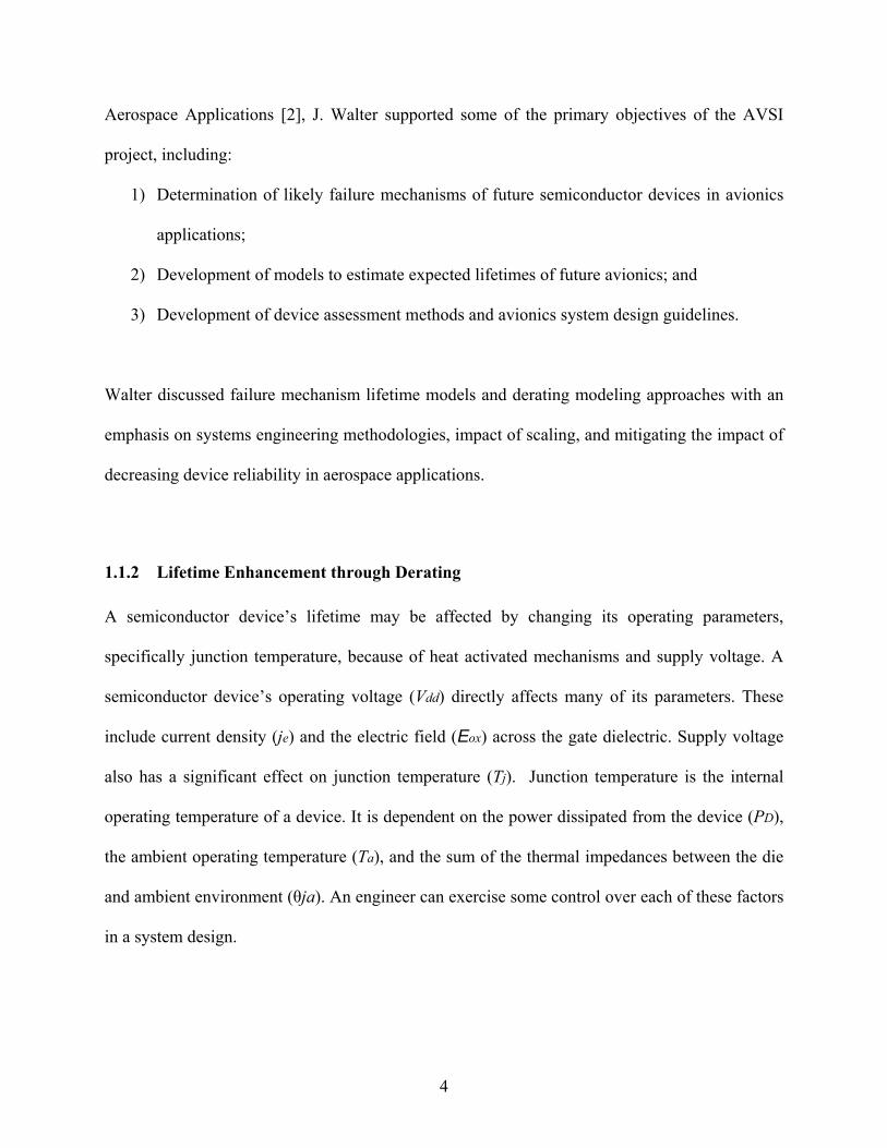
degradation (HCD), time-dependent-dielectric-breakdown (TDDB), and derating factor vs.
derated voltage while keeping operating temperature and frequency constant in Figure 1. In the
case of the three intrinsic wearout mechanisms discussed, the combined total derating factor is
described by Walter as:
fTDDB
TDDB
fHCD
HCD
fEM
EMf
DDD
Dλλλ
λ
++= (1.6)
where λ can represent either the total failure rate or the sum of the failure rates of the wearout
mechanisms. This will result in two different answers, the total derating factor and wearout
derating factor respectively.
7
Figure 1. Df versus Dvoltage with Constant Operating Temperature and Frequency. λEM = λTDDB =λHCD, Tj = 85°C, Ta = 20°C, Vdd,max = 3.3V, Vth = 0.8V, EaEM = 0.8 eV, n = 2, B = 70, EaTDDB = 0.75 eV, Eox = 4 MV/cm, g = 3 Naperians per MV/cm.
Due to the low failure rates of semiconductor devices, a device’s failure rate is normally
determined through accelerated life testing and then extrapolated back to at-use conditions, using
an acceleration factor, in order to approximate an MTTF. When accelerated life testing is used to
determine the rated lifetime of a device, care must be taken to ensure that all the relevant failure
mechanisms are accelerated in order to make a reasonable extrapolation of the device’s failure
rate.
1.1.4 Failure Mechanism Simulation
Over the years, there has been a significant amount of simulation work that focuses on individual
failure mechanisms and their impact on semiconductor reliability. Of note, Hsu, et al. [7] and
8
Chun, et al. [8] developed CAD tools for hot carrier induced damage effects in VLSI circuits;
Alam, et. al. [9] developed models to simulate microelectronic reliability from electromigration
damage; and P.C. Li, et al. [10] studied the effect of oxide failure on microelectronic reliability
using simulation. Electromigration and hot-carrier effects on performance degradation of a 2-
stage op-amp were simulated on a CAD reliability tool integrated with a Cadence Spectre
simulator by Xuan and Chatterjee [11].
Attempts have been made over the years to simulate multiple failure mechanisms in
microelectronics. Some of the earlier ones include Lathrop, et al. [12] who provided an
investigative program using a CAD tool to improve microelectronic reliability by generating
failure information due to electromigration, charge injection and electrostatic discharge; in 1992,
Hu [13] developed a circuit reliability simulation model called BERT, that simulates the hot
electron effect, oxide time-dependent breakdown, electromigration, bipolar transistor gain
degradation, and radiation effects on microelectronics as part of the design process. As
simulators became more advanced, more sophisticated approaches to modeling device
performance and reliability were developed.
1.1.5 Micro-Architectural Level Reliability Modeling
While junction temperature reduction has traditionally been the primary derating focus, various
SRAM field studies of commercial devices, and experimental research and modeling of the
effects of duty cycle and Vdd stresses on the device, suggest that derating these elements with Tj
can provide an order of magnitude or more improvement in reliability (FIT) [14-16]. The circuit
design and application, however, must be robust enough to operate at the lower end of the device
9
performance and specification limits. In 2004, J. Srinivasan and the University of Illinois [17]
conducted processor RAMP modeling which provided FIT estimates across 180nm to 65nm
technologies for a processor operating at worst case conditions. The impact of different scaling
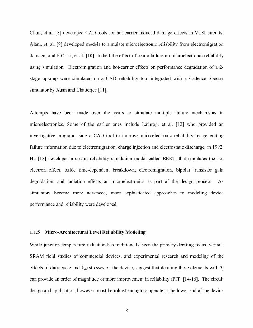
related parameters on intrinsic failure mechanisms is presented in Table 1 [17]. FIT estimates
for TDDB, EM, Stress Migration (SM) and Thermal Cycling (TC) related failure mechanisms,
and their relative contribution to total FIT are summarized in Figure 2. On average, the simulated
failure rate (FR) of a scaled 65nm processor may be as high as 316% higher than a similarly
pipelined 180nm device [17].
Table 1. Impact of Different Scaling Related Parameters on Intrinsic Failure Mechanisms.
Figure 2. FIT Values for Processor W/C Conditions. Application for Model (a) and Model (b) with Relative Contribution of Each Mechanism.
10
Generally accepted models for MTTF due to EM, SM, TDDB and TC used in Srinivasan’s
model have been published in JEDEC Publication JEP122-A [18] and are recapitulated here for
completeness:
( ) kTE
nfEM
aEM
Jt exp−∝ (1.7)
where J is the current density in the interconnect, EaEM is the activation energy for
electromigration, k is Boltzmann's constant, and T is absolute temperature in Kelvin. n and EaEM
are constants that depend on the interconnect metal used.
kTE
mofSM
aSM
TTt exp−
−∝ (1.8)
where T is the absolute temperature in Kelvin, To is the stress free temperature of the metal (the
metal deposition temperature), and m and EaSM are material dependent constants.
kT
ZTTYXbTa
fTDDB Vt
⎟⎠⎞
⎜⎝⎛ ++
−
⎟⎠⎞
⎜⎝⎛∝ exp1 (1.9)
where T is the absolute temperature in Kelvin, a, b, X, Y, and Z are fitting parameters, and V is
the voltage.
q
ambientaveragefTC TT
t ⎟⎟⎠
⎞⎜⎜⎝
⎛
−∝
1 (1.10)
11
where Tambient is the ambient temperature in Kelvin, Taverage – Tambient is the average large thermal
cycle experienced by a structure on a chip, and q is the Coffin-Manson exponent, an empirically
determined material-dependent constant.
Srinivasan makes two specific contributions. First, he describes an architecture-level model and
its implementation, called RAMP, which can dynamically track lifetime reliability responding to
changes in application behavior. RAMP is based on state-of-the-art device models for different
wearout mechanisms. Second, he proposes dynamic reliability management (DRM) - a technique
where a processor can respond to changing application behavior to maintain its lifetime
reliability target. Contrary to current worst-case behavior based reliability qualification
methodologies, DRM allows processors to be qualified for reliability at lower (but more likely)
operating points than the worst case.
1.1.6 Circuit-Level Reliability Modeling and Simulation
There has been work over the years that has focused on the impact of intrinsic failure
mechanisms on the circuit. Kumar, et al. [19] modeled NBTI degradation of threshold voltage
and static noise margin (SNM) on 100nm and 70nm SRAM cells. In 2002, Reddy, et al. [20]
demonstrated that SNM of an SRAM memory cell degrades on an 130nm CMOS process by
NBTI and that the relative degradation increases as the operating voltage decreases. This was
confirmed by measuring an increase in the relative frequency degradation of an NBTI stressed
ring oscillator as the operating voltage dropped. Jha, et al. [21] later attempted to quantify circuit
level degradation due to NBTI by simulating a variety of analog/mixed signal circuits.
12
In addition to hot carrier effects on circuit level reliability, thin oxide reliability in scaled CMOS
devices has been modeled to predict breakdown at the device level and to determine the impact
on circuit performance. J. Stathis describes this approach in [22] and explains how soft
breakdown is the most common mode for a constant-current stress, while hard breakdown
generally occurs during constant-voltage stress. Rosenbaum, et al. [23] also developed a circuit
reliability simulator oxide breakdown module.
Khin, et al. [24] worked on a circuit reliability simulator for interconnects and contact
electromigration.
1.1.7 Deep Submicron CMOS VLSI Circuit Reliability Modeling and Simulation
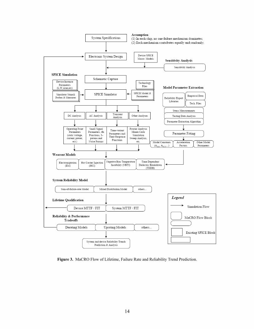
A new SPICE reliability simulation methodology that shifts the focus of reliability analysis from
device wearout to circuit functionality was developed in 2005 by X. Li [25]. A set of
accelerated lifetime models and failure equivalent circuit models were proposed for the most
common MOSFET intrinsic wearout mechanisms, including hot carrier injection (HCI), negative
bias temperature instability (NBTI), and TDDB. The accelerated lifetime models help to identify
the most degraded transistors in a circuit in terms of the device's terminal voltage and current
waveforms. Corresponding failure equivalent circuit models are then incorporated into the circuit
to substitute the identified transistors. Finally, SPICE simulation is performed again to check
circuit functionality and analyze the impact of device wearout on circuit operation. Device
wearout effects are lumped into a very limited number of failure equivalent circuit model
parameters, and circuit performance degradation and functionality are determined by the
magnitude of these parameters.
13
In Li’s approach, it is unnecessary to perform a large number of small-step SPICE simulation
iterations, making simulation time much shorter in comparison to other tools. In addition, a
reduced set of failure equivalent circuit model parameters, rather than a large number of device
SPICE model parameters, need to be accurately characterized at each interim wearout process.
Thus, device testing and parameter extraction work are also significantly simplified. The
Maryland Circuit Reliability Oriented (MaCRO) SPICE simulation methodology flow is
summarized in Figure 3 [25].
14
Figure 3. MaCRO Flow of Lifetime, Failure Rate and Reliability Trend Prediction.
15
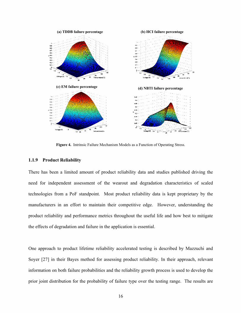
1.1.8 Physics-of-Failure Based VLSI Circuits Reliability Simulation and Prediction
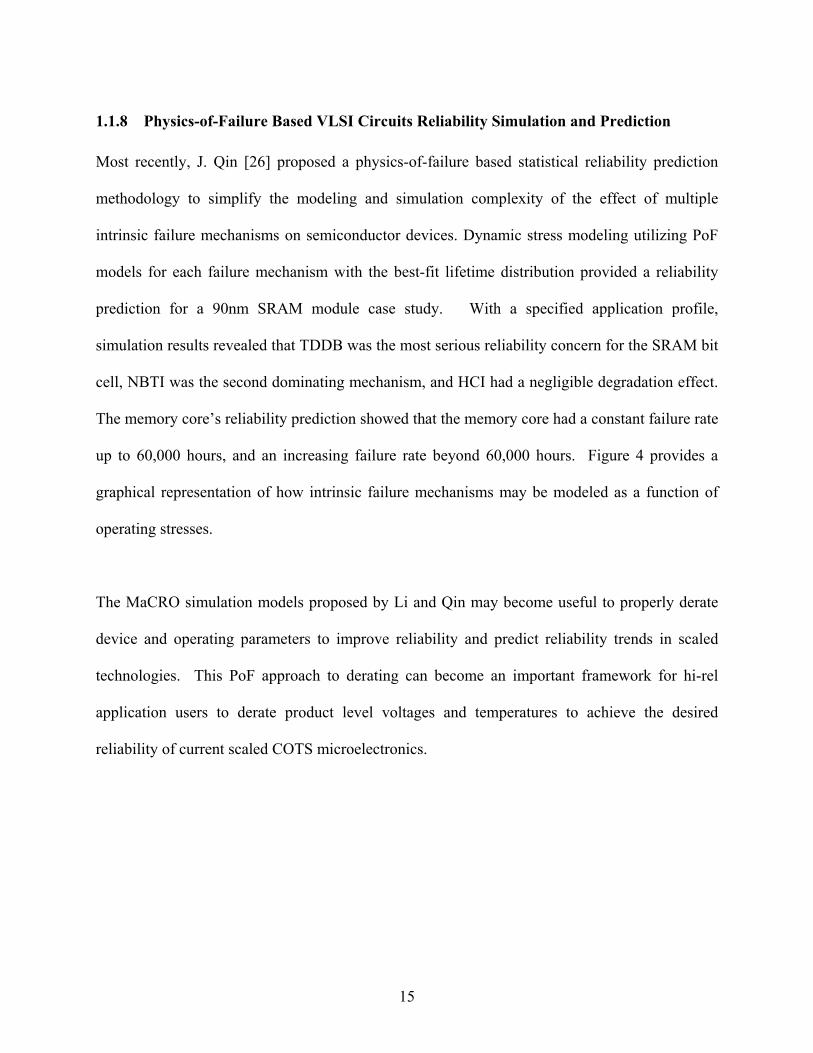
Most recently, J. Qin [26] proposed a physics-of-failure based statistical reliability prediction
methodology to simplify the modeling and simulation complexity of the effect of multiple
intrinsic failure mechanisms on semiconductor devices. Dynamic stress modeling utilizing PoF
models for each failure mechanism with the best-fit lifetime distribution provided a reliability
prediction for a 90nm SRAM module case study. With a specified application profile,
simulation results revealed that TDDB was the most serious reliability concern for the SRAM bit
cell, NBTI was the second dominating mechanism, and HCI had a negligible degradation effect.
The memory core’s reliability prediction showed that the memory core had a constant failure rate
up to 60,000 hours, and an increasing failure rate beyond 60,000 hours. Figure 4 provides a
graphical representation of how intrinsic failure mechanisms may be modeled as a function of
operating stresses.
The MaCRO simulation models proposed by Li and Qin may become useful to properly derate
device and operating parameters to improve reliability and predict reliability trends in scaled
technologies. This PoF approach to derating can become an important framework for hi-rel
application users to derate product level voltages and temperatures to achieve the desired
reliability of current scaled COTS microelectronics.
16
Figure 4. Intrinsic Failure Mechanism Models as a Function of Operating Stress.
1.1.9 Product Reliability
There has been a limited amount of product reliability data and studies published driving the
need for independent assessment of the wearout and degradation characteristics of scaled
technologies from a PoF standpoint. Most product reliability data is kept proprietary by the
manufacturers in an effort to maintain their competitive edge. However, understanding the
product reliability and performance metrics throughout the useful life and how best to mitigate
the effects of degradation and failure in the application is essential.
One approach to product lifetime reliability accelerated testing is described by Mazzuchi and
Soyer [27] in their Bayes method for assessing product reliability. In their approach, relevant
information on both failure probabilities and the reliability growth process is used to develop the
prior joint distribution for the probability of failure type over the testing range. The results are
(a) TDDB failure percentage (b) HCI failure percentage
(d) NBTI failure percentage(c) EM failure percentage
17
then used at a particular test stage to update the knowledge of the probability of each failure type
and the product reliability of the current test stage and subsequent test stages. Jee, et al. [28]
developed an approach to optimize test coverage and test application time of an embedded
SRAM using a defect-based approach, e.g., shorts and opens in a memory cell array. In their
approach, faults are extracted and analyzed from a representative portion of the array, and the
results are replicated for the entire memory array to reduce test time.
Estimating long-term performance of scaled microelectronic products can be difficult because
accelerated life testing (ALT) involving elevated stresses can often result in either too few or no
failures to make realistic predictions or inferences. Tang, et al. [29] describes a methodology to
overcome this problem by using accelerated degradation testing (ADT) as a means to predict
performance in such cases. By identifying key performance measures which are expected to
degrade over time, product reliability can be inferred by the degradation paths without observing
actual physical failures. Using this approach, the user defines a failure as the first time a key
performance measure exceeds a pre-specified threshold, and then the degradation path is
correlated to product reliability.
Krasich [30] and Turner [31] discuss product reliability and accelerated testing in their work, and
Turner addresses failure mitigation and challenges as microelectronics scale to 90nm and
beyond. Other notable accelerated degradation modeling methodologies include: the statistical
methods of using degradation measures to estimate the time-to-fail distribution for a variety of
degradation models developed by Lu and Meeker [32]; a model for analyzing linear degradation
data proposed by Lu, et al. [33]; and the method to handle degradation failures developed by Guo
18
and Mettas [34] by applying amplification factors with control factors to model the degradation
process.
1.2 CMOS Technology Scaling and Impact
Over the past three decades, CMOS technology scaling has been a primary driver of the
electronics industry and has provided a path toward both denser and faster integration [35-47].
The transistors manufactured today are twenty times faster and occupy less than 1% of the area
of those built twenty years ago. Predictions of size reduction limits have proven to elude the
most insightful scientists and researchers. The predicted ‘limit’ has been dropping at nearly the
same rate as the size of the transistors.
The number of devices per chip and the system performance has been improving exponentially
over the last two decades. As the channel length is reduced, the performance improves, the
power per switching event decreases, and the density improves. But the power density, total
circuits per chip, and the total chip power consumption have been increasing. The need for more
performance and integration has accelerated the scaling trends in almost every device parameter,
such as lithography, effective channel length, gate dielectric thickness, supply voltage, and
device leakage. Some of these parameters are approaching fundamental limits, and alternatives to
the existing material and structures may need to be identified in order to continue scaling.
1.2.1 MOS Scaling Theory
During the early 1970s, both Mead [35] and Dennard [36] noted that the basic MOS transistor
structure could be scaled to smaller physical dimensions. One could postulate a “scaling factor”
19
of λ, the fractional size reduction from one generation to the next generation, and this scaling
factor could then be directly applied to the structure and behavior of the MOS transistor in a
straightforward multiplicative fashion. For example, a CMOS technology generation could have
a minimum channel length Lmin, along with technology parameters such as the oxide thickness
tox, the substrate doping NA, the junction depth xj, the power supply voltage Vdd, the threshold
voltage Vth, etc. The basic “mapping” to the next process, Lmin→ λLmin, involved the concurrent
mappings of tox→ λtox, NA→ λNA, xj→ λxj, Vdd→ λVdd, and Vth→ λVth. Thus, the structure of the
next generation process could be known beforehand, and the behavior of circuits in that next
generation could be predicted in a straightforward fashion from the behavior in the present
generation. The scaling theory developed by Mead and Dennard is solidly grounded in the basic
physics and behavior of the MOS transistor. Scaling theory allows a “photocopy reduction”
approach to feature size reduction in CMOS technology, and while the dimensions shrink,
scaling theory causes the field strengths in the MOS transistor to remain the same across
different process generations. Thus, the “original” form of scaling theory is constant field
scaling.
Constant field scaling requires a reduction of the power supply voltage with each technology
generation. In the 1980s, CMOS adopted the 5V power supply, which was compatible with the
power supply of bipolar TTL logic. Constant field scaling was replaced with constant voltage
scaling, and instead of remaining constant, the fields inside the device increased from generation
to generation until the early 1990s, when excessive power dissipation and heating, gate
dielectrics TDDB, and channel hot carrier aging caused serious problems with the increasing
electric field. As a result, constant field scaling was applied to technology scaling in the 1990s.
20
Constant field scaling requires that the threshold voltage be scaled in proportion to the feature
size reduction. However, ultimately threshold voltage scaling is limited by the sub-threshold
slope of the MOS transistor, which itself is limited by the thermal voltage kT/q, where the
Boltzmann constant, k and the electron charge, q are fundamental constants of nature and cannot
be changed. The choice of the threshold voltage in a particular technology is determined by the
off-state current goal per transistor and the sub-threshold slope. With off-current requirements
remaining the same (or even tightening) and the sub-threshold slope limited by basic physics, the
difficulty with scaling the threshold voltage is clear. Because of this, the power supply voltage
decreased corresponding with the constant field scaling, but the threshold voltage was unable to
scale as aggressively. This situation worsens as feature sizes and power supply voltages continue
to scale. This is a fundamental problem with further CMOS technology scaling.
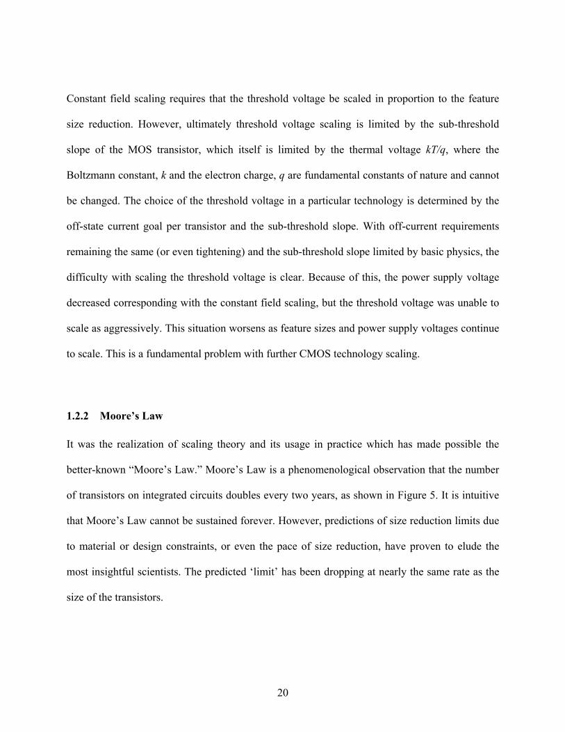
1.2.2 Moore’s Law
It was the realization of scaling theory and its usage in practice which has made possible the
better-known “Moore’s Law.” Moore’s Law is a phenomenological observation that the number
of transistors on integrated circuits doubles every two years, as shown in Figure 5. It is intuitive
that Moore’s Law cannot be sustained forever. However, predictions of size reduction limits due
to material or design constraints, or even the pace of size reduction, have proven to elude the
most insightful scientists. The predicted ‘limit’ has been dropping at nearly the same rate as the
size of the transistors.
21
Figure 5. Moore’s Law.
1.2.3 Scaling to its Limits
There does not seem to be any fundamental physical limitation that would prevent Moore’s Law
from characterizing the trends of integrated circuits. However, sustaining this rate of progress is
not straightforward [39].
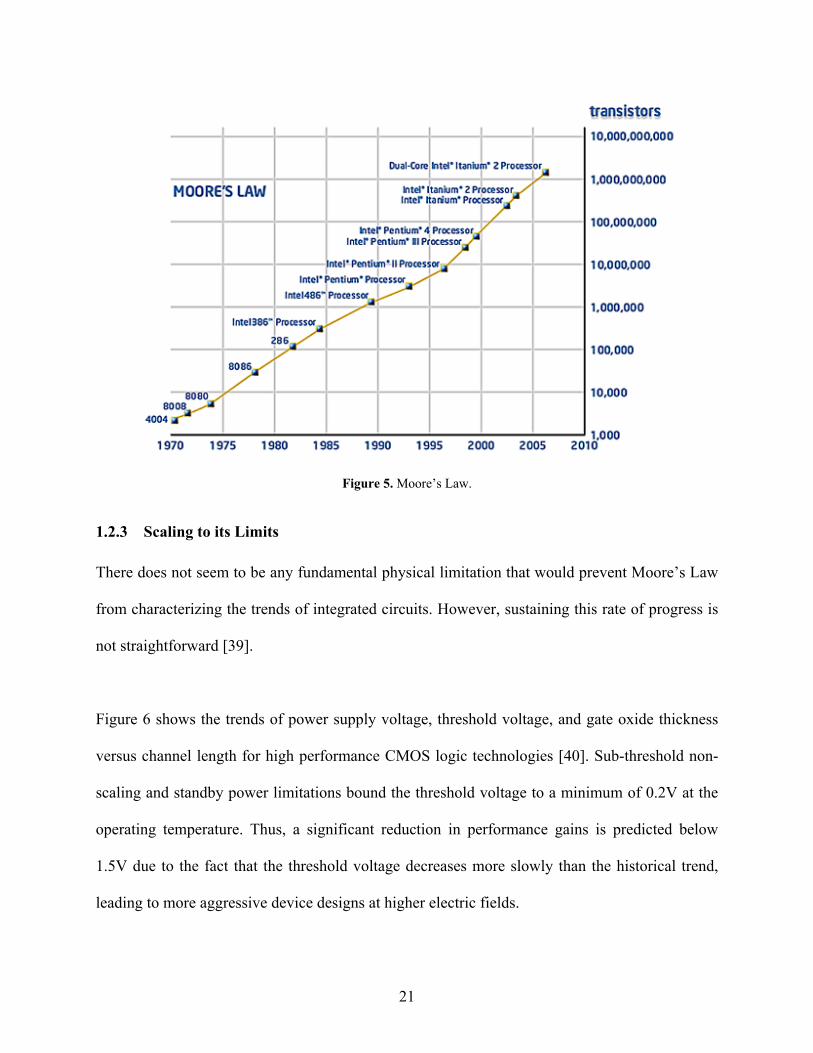
Figure 6 shows the trends of power supply voltage, threshold voltage, and gate oxide thickness
versus channel length for high performance CMOS logic technologies [40]. Sub-threshold non-
scaling and standby power limitations bound the threshold voltage to a minimum of 0.2V at the
operating temperature. Thus, a significant reduction in performance gains is predicted below
1.5V due to the fact that the threshold voltage decreases more slowly than the historical trend,
leading to more aggressive device designs at higher electric fields.
22
Figure 6. Trends of Power Supply Voltage Vdd, Threshold Voltage Vth, and Gate Oxide Thickness tox, versus Channel Length for CMOS Logic Technologies. Further technology scaling requires major changes in many areas, including: 1) improved
lithography techniques and non-optical exposure technologies; 2) improved transistor design to
achieve higher performance with smaller dimensions; 3) migration from current bulk CMOS
devices to novel materials and structures, including silicon-on-insulator, strained Si and novel
dielectric materials; 4) circuit sensitivity to soft errors from radiation; 5) smaller wiring for on-
chip interconnection of the circuits; 6) stable circuits; 7) more productive design automation
tools; 8) denser memory cells, and 9) manageable capital costs. Metal gate and high-k gate
dielectrics were introduced into production in 2007 to maintain technology scaling trends [48].
In addition, packaging technology needs to progress at a rate consistent with on-going CMOS
technology scaling at sustainable cost/performance levels. This requires advances in I/O density,
23
bandwidth, power distribution, and heat extraction. System architecture will also be required to
maximize the performance gains achieved in advanced CMOS and packaging technologies.
1.2.4 Scaling Impact on Circuit Performance
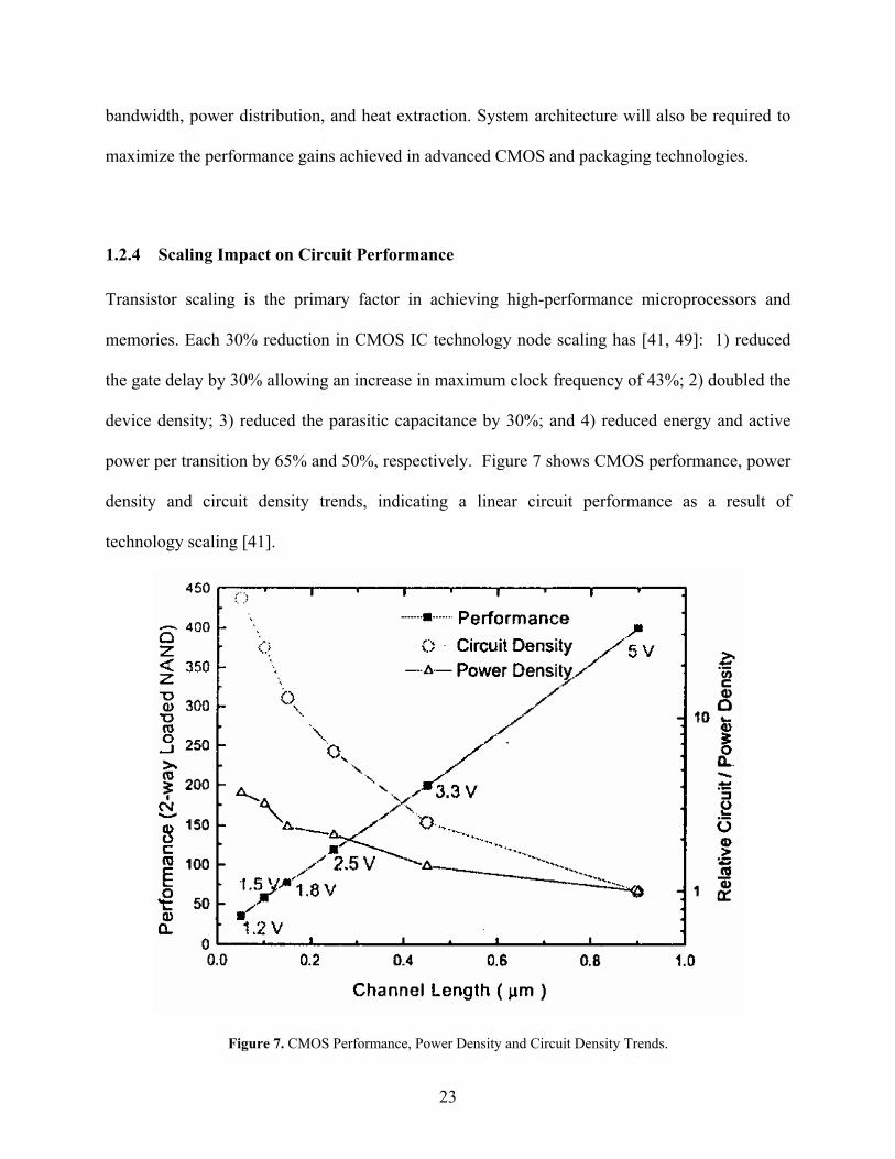
Transistor scaling is the primary factor in achieving high-performance microprocessors and
memories. Each 30% reduction in CMOS IC technology node scaling has [41, 49]: 1) reduced
the gate delay by 30% allowing an increase in maximum clock frequency of 43%; 2) doubled the
device density; 3) reduced the parasitic capacitance by 30%; and 4) reduced energy and active
power per transition by 65% and 50%, respectively. Figure 7 shows CMOS performance, power
density and circuit density trends, indicating a linear circuit performance as a result of
technology scaling [41].
Figure 7. CMOS Performance, Power Density and Circuit Density Trends.
24
1.2.5 Scaling Impact on Power Consumption
Dynamic power and leakage current are the major sources of power consumption in CMOS
circuits. Leakage related power consumption has become more significant as threshold voltage
scales with technology. There are several studies that deal with the impact of technology scaling
in various aspects of CMOS VLSI design [39, 47, 50-52].
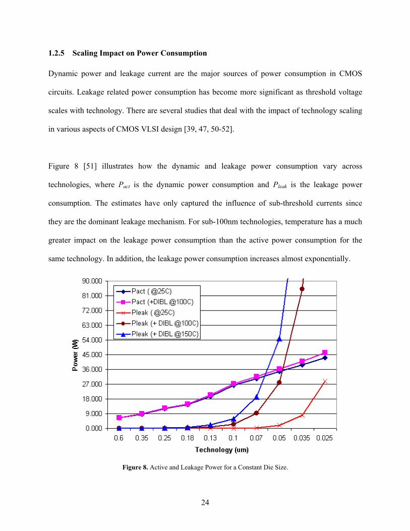
Figure 8 [51] illustrates how the dynamic and leakage power consumption vary across
technologies, where Pact is the dynamic power consumption and Pleak is the leakage power
consumption. The estimates have only captured the influence of sub-threshold currents since
they are the dominant leakage mechanism. For sub-100nm technologies, temperature has a much
greater impact on the leakage power consumption than the active power consumption for the
same technology. In addition, the leakage power consumption increases almost exponentially.
Figure 8. Active and Leakage Power for a Constant Die Size.

25
1.2.6 Scaling Impact on Circuit Design
With continuing aggressive technology scaling, it is increasingly difficult to sustain supply and
threshold voltage scaling to provide the required performance increase, limit energy
consumption, control power dissipation, and maintain reliability. These requirements pose
several difficulties across a range of disciplines. On the technology front, the question arises
whether we can continue along the traditional CMOS scaling path – reducing effective oxide
thickness, improving channel mobility, and minimizing parasitics. On the design front,
researchers are exploring various circuit design techniques to deal with process variation,
leakage and soft errors [41, 47].
For CMOS technologies beyond 90nm, leakage power is one of the most crucial design
components which must be efficiently controlled in order to utilize the performance advantages
of these technologies. It is important to analyze and control all components of leakage power,
placing particular emphasis on sub-threshold and gate leakage power. A number of issues must
be addressed, including low voltage circuit design under high intrinsic leakage, leakage
monitoring and control, effective transistor stacking, multi-threshold CMOS, dynamic threshold
CMOS, well biasing techniques, and design of low leakage data-paths and caches.
While supply voltage scaling becomes less effective in providing power savings as leakage
power becomes larger due to scaling, it is suggested that the goal is to no longer have simply the
highest performance, but instead have the highest performance within a particular power budget
by considering the physical aspects of the design. In some cases, it may be possible to balance
the benefit of using high threshold devices from a low leakage process running at the higher
26
possible frequency at a full Vdd, as opposed to using faster but leakier devices which require
more voltage scaling in order to reach the desired power budget.
Nanometer design technologies must work under tight operating margins, and are therefore
highly susceptible to any process and environmental variability. Traditional sources of variation
due to circuit and environmental factors, such as cross capacitance, power supply integrity,
multiple inputs switching, and errors arising due to tools and flows, affect circuit performance
significantly. To address environmental variation, it is important to build circuits that have well-
distributed thermal properties, and to carefully design supply networks to provide reliable Vdd
and ground levels throughout the chip.
With technology scaling, process variation has become more of a concern and has received an
increased amount of attention from the design automation community. Several research efforts
have addressed the issue of process variation and its impact on circuit performance [49, 53-55].
A worst-case approach was first used to develop the closed form models for sensitivity due to
different parameter variations for a clock tree [53], and was further developed to include
interconnect and device variation impact on timing delay due to technology scaling [49]. The
impact of systematic variation sources was then considered in [54]. Finally, an integrated
variation analysis technique was developed in [55], which considers the effects of both
systematic and random variation in both interconnect and devices simultaneously. The design
community has realized that in order to address the process-induced variations and to ensure the
final circuit reliability, instead of treating timing in a worst-case manner, as is conventionally
done in static timing analysis, statistical techniques need to be employed that directly predict the
27
percentage of circuits that are likely to meet a timing specification. The effects of uncertainties in
process variables must be modeled using statistical techniques, and they must be utilized to
determine variations in the performance parameters of a circuit.
1.2.7 Scaling Impact on Parts Burn-In
Power supply voltage in scaled technologies must be lowered for two main reasons [56]: 1) to
reduce the device internal electric fields and 2) to reduce active power consumption since it is
proportional to Vdd2. As Vdd scales, then Vth must also be scaled to maintain drain current
overdrive to achieve higher performance. Lower Vth leads to higher off-state leakage current,
which is the major problem with burn-in of scaled nanometer technologies.
The total power consumption of high-performance microprocessors increases with scaling. Off-
state leakage current is a higher percentage of the total current at the sub-100nm nodes under
nominal conditions. The ratio of leakage to active power becomes worse under burn-in
conditions and the dominant power consumption is from the off-state leakage. Typically, clock
frequencies are kept in the tens of megahertz range during burn-in, resulting in a substantial
reduction in active power. Conversely, the voltage and temperature stresses cause the off-state
leakage to be the dominant power component.
Stress during burn-in accelerates the defect mechanisms responsible for early-life failures.
Thermal and voltage stresses increase the junction temperature resulting in accelerated aging.
Elevated junction temperature, in turn, causes leakages to further increase. In many situations,
this may result in positive feedback leading to thermal runaway. Such situations are more likely
28
to occur as technology is scaled into the nanometer region. Thermal runaway increases the cost
of burn-in dramatically. To avoid thermal runaway, it is crucial to understand and predict the
junction temperature under normal and stress conditions. Junction temperature, in turn, is a
function of ambient temperature, package to ambient thermal resistance, package thermal
resistance, and static power dissipation. Considering these parameters, one can optimize the
burn-in environment to minimize the probability of thermal runaway while maintaining the
effectiveness of burn-in test.
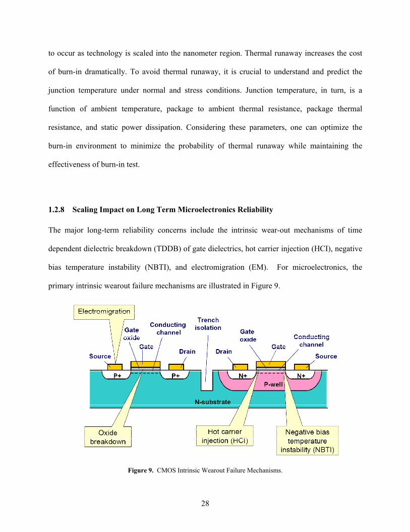
1.2.8 Scaling Impact on Long Term Microelectronics Reliability
The major long-term reliability concerns include the intrinsic wear-out mechanisms of time
dependent dielectric breakdown (TDDB) of gate dielectrics, hot carrier injection (HCI), negative
bias temperature instability (NBTI), and electromigration (EM). For microelectronics, the
primary intrinsic wearout failure mechanisms are illustrated in Figure 9.
Figure 9. CMOS Intrinsic Wearout Failure Mechanisms.
29
The drivers & effects of the primary intrinsic failure mechanisms of concern are as follows:
Hot Carrier Injection (HCI):
• Drivers: Channel length & width, oxide thickness, operating voltage, and low
temperature.
• Effect: Increased substrate current (Isub), saturation drain current degradation (IDSAT), and
increase in Vth.
• Impact of Scaling: The rate of hot carrier degradation is directly related to the length of
the channel, the oxide thickness, and the voltage of the device. Hot carrier effects are
expected to be a growing concern.
Electromigration (EM):
• Drivers: High temperature and current density in metal interconnects.
• Effect: Metal migration leading to increased resistance and open or short circuit.
• Impact of Scaling: Energy densities within interconnects are expected to grow as device
features become smaller.
Negative Bias Temperature Instability (NBTI):
• Drivers: Oxide thickness and high temperature.
• Effect: Degraded (IDSAT) and transconductance (gm), and an increase in Ioff and Vth.
• Impact of Scaling: NBTI is a growing concern as devices continue to scale. As feature
sizes scaled through 0.13um, devices required much thinner gate oxides and introduced
nitrides in the SiO2.
30
Time-Dependent-Dielectric-Breakdown (TDDB):
• Drivers: Oxide thickness, gate voltage, and high electric field.
• Effect: Anode to cathode short through the dielectric.
• Impact of Scaling: TDDB is expected to accelerate as gate oxide thicknesses decrease
with continued device scaling.
The physics and the reliability characterization and modeling of each mechanism have been
major research topics for the past three decades. There has been an abundant amount of research
in this area, including [57].
Among the wear-out mechanisms, TDDB and NBTI seem to be the major reliability concerns as
devices scale. The gate oxide has been scaled down to only a few atomic layers thick with
significant tunneling leakage. While the gate leakage current may be at a negligible level
compared with the on-state current of a device, it will first have an effect on the overall standby
power. For a total active gate area of 0.1 cm2, chip standby power limits the maximum tolerable
gate leakage current to approximately 1-10 A/cm2, which occurs for gate oxides in the range of
15-18A [40].
Scaling impact of TDDB and NBTI on digital, analog and RF circuit reliability has been an
important topic during past years [58-69]. Either TDDB, NBTI, or both were found to contribute
to digital circuit speed degradation [58, 62], FPGA delay increase [65], SRAM minimum
operating voltage Vmin shift measurement [64, 66, 67], RF circuit parametric drifts [60, 61], and
analog circuit mismatch [59, 63]. It appears that SRAM minimum operating voltage Vmin shift
31
due to TDDB and NBTI is one of the effects that has been tested and characterized most. For
example, it is shown [66] that transistor shifts due to NBTI manifest themselves as population
tails in the product’s minimum operating voltage distribution. TDDB manifests itself as single-
bit or logic failures that constitute a separate sub-population. NBTI failures are characterized by
Log-normal statistics combined with a slower degradation rate, which is in contrast to TDDB
failures that follow extreme-value statistics and exhibit a faster degradation rate. Most of the
studies seem to indicate that the advanced technology parts may experience intrinsic or wear-out
mechanisms induced circuit parametric shifts during operating life time, especially at higher
operating voltages and temperature conditions.
1.3 Physics-of-Failure (PoF) Methodology
The PoF methodology may be summarized as follows:
• Identify potential failure mechanisms (e.g., chemical, electrical, physical, mechanical,
structural, or thermal processes leading to failure) and the likely failure sites on each
device.
• Expose the product to highly accelerated stresses to find the dominant root-cause of
failure.
• Identify the dominant failure mechanism as the weakest link.
• Model the dominant mechanism (what and why the failure takes place).
• Combine the data gathered from the acceleration tests and statistical distributions, e.g.,
Weibull, lognormal distributions.
32
• Develop an equation for the dominant failure mechanism at the site and its time-to-failure
(TTF).
• Extrapolate to use conditions.
This process is used to assess the retention time reliability of three progressive DRAM
technologies described in Chapter 2.
1.3.1 Competing Mechanism Theory
While the failure rate qualification has not improved over the years, the semiconductor industry
understanding of reliability physics of semiconductor devices has increased tremendously.
Failure mechanisms are well understood and the manufacturing and design processes are so
tightly controlled that electronic components are designed to perform with reasonable life and
with no single dominant failure mechanism. In practice, however, highly accelerated stress
testing is used to determine the life limiting failure mechanism and the weakest link.
1.3.2 Intrinsic Failure Mechanism Overview
The potential intrinsic wearout failure mechanisms considered include Hot Carrier Injection
(HCI), Electromigration (EM), Negative Bias Temperature Instability (NBTI), and Time-
Dependent-Dielectric-Breakdown (TDDB). Much work has been done on the physics of these
failure mechanisms in the past including [70], a primary deliverable for the Aerospace Vehicles
Space Institute (AVSI) Consortium Project 17: Methods to Account for Accelerated
Semiconductor Wearout. Therefore; only a brief overview will be presented here.
33
1.3.3 Hot Carrier Injection and Statistical Model
The switching characteristics of a MOSFET can degrade and exhibit instabilities due to the
charge that is injected into the gate oxide. The typical effect of hot carrier, or hot electron,
degradation is to reduce the on-state current in an n-channel MOSFET and increase the off-state
current in a p-channel MOSFET. The rate of hot carrier degradation is directly related to the
length of the channel, the oxide thickness, and the voltage of the device. A measure of transistor
degradation or lifetime is commonly defined in terms of percentage shift of threshold voltage,
change in transconductance, or variation in drive or saturation current [71]. Several approaches
to minimize HCI effects include: thermo-chemical processing to reduce the Si-SiO2 interfacial
trap density; introducing ion implanted regions of lighter doping between the channel and
heavily doped drain regions to better distribute the electric field, reducing its peak value; adding
nitride to the gate oxide so that it is more resistant to interface-trap generation; and reducing the
transistor operating voltage [71].
There are three main types of hot carrier injection modes according to Takeda [72]:
1. Channel hot electron (CHE) injection.
2. Drain avalanche hot carrier (DAHC) injection.
3. Secondary generated hot electron (SGHE) injection.
CHE injection is due to the escape of “lucky” electrons from the channel, causing a significant
degradation of the oxide and the Si−SiO2 interface, especially at low temperature (77K) [73].
Alternatively, DAHC injection results in both electron and hole gate currents due to impact
ionization, giving rise to the most severe degradation around room temperature. SGHE injection
34
is due to minority carriers from secondary impact ionization or, more likely, bremsstrahlung
radiation, and becomes a problem in ultra-small MOS devices.
The lognormal distribution is generally used to model hot carrier degradation [74]:
⎥⎥⎦
⎤
⎢⎢⎣
⎡⎟⎠⎞
⎜⎝⎛ −−
Π=
2
2/1
ln21exp
)2(1)(
σμ
σt
ttf . (1.11)
Hot carrier effects are enhanced at low temperature. The primary reason for this is an increase in
electron mean free path and impact ionization rate at low temperature. As was shown in [75],
substrate current at 77K is five times greater than that at room temperature, and CHE gate
current is approximately 1.5 orders of magnitude greater than that at room temperature. At low
temperature, the electron trapping efficiency increases and the effect of fixed charges becomes
large [76]. This accelerates the degradation of Gm at low temperature. The degradation of Vth and
Gm at low temperatures is more severely accelerated for CHE-induced effects than for DAHC.
Hu [77] showed the temperature coefficient of CHE gate and substrate current to be negative.
The lifetime model for HCI is commonly expressed as:
⎟⎠⎞
⎜⎝⎛
⎟⎠⎞
⎜⎝⎛=
−
kTE
WIAt aHCI
nsub
HCIf exp , (1.12)
where Ea has a value of approximately −0.1 eV ~ −0.2 eV [78].
35
1.3.4 Electromigration and Statistical Model
Passage of high current densities through interconnects causes time-dependent mass transport
effects that manifest as surface morphological changes. The resulting metal conductor
degradation includes mass pileups in hillocks and whiskers, void formation and thinning,
localized heating, and cracking of passivating dielectrics [71]. The scaling of interconnects to
keep up with semiconductor scaling increases current densities and temperature, reducing
median life. There are three properties having an immediate impact on EM reliability models:
• The orientation of the boundary with respect to the electric field.
• The angles of the grain boundaries with respect to each other.
• Changes in the number of the grains per unit area–grain density.
Each of these properties can give rise to the ion divergences necessary to create voids in metal
strips and interconnects.
The lognormal failure distribution is often used to characterize EM lifetime [79]. The bimodal
lognormal distribution is often seen in copper via EM tests. Lai [80] described two EM failure
mechanisms: via related and metal-stripe related. Ogawa [81] reported two distinct failure modes
in dual-damascene Cu/oxide interconnects. One model described void formation within the dual-
damascene via; the other reflected voiding that occurs in the dual-damascene trench. These
models formed a bimodal lognormal distribution.
36
The temperature acceleration factor is calculated from Black’s equation and may be expressed
as:
⎟⎟⎠
⎞⎜⎜⎝
⎛⎟⎠⎞
⎜⎝⎛ −⎟⎟
⎠
⎞⎜⎜⎝
⎛==
21
211exp1
TTkE
jj
AFtMTTF a
sm
, (1.13)
where tm = test time to failure, j = current density, T1 and T2 are stress operating temperatures,
and Ea is the activation energy for electromigration. Reported activation energies for EM range
from approximately 0.35eV ~ 0.9eV depending on conductor grain size and metal alloy [82].
1.3.5 Negative Bias Temperature Instability and Statistical Model
NBTI occurs to p-channel MOS (PMOS) devices under negative gate voltages at elevated
temperatures. Bias temperature stress under constant voltage (DC) causes the generation of
interface traps (NIT) between the gate oxide and silicon substrate, which causes device threshold
voltage (Vt) to increase, and drain current (Idsat) and transconductance (gm) to decrease. The
NBTI effect is more severe for PMOS than NMOS devices due to the presence of holes in the
PMOS inversion layer that are known to interact with the oxide states. The degradation of device
performance is a significant reliability concern for current ultrathin gate oxides where there are
indications that NBTI worsens exponentially with thinning gate oxide. Degradation is
commonly modeled with power-law time dependence and Arrhenius temperature acceleration.
Degradation partially recovers once stress is removed [83]. Major drivers for NBTI degradation
in PMOS devices are ultrathin gate oxide thickness and high temperature.
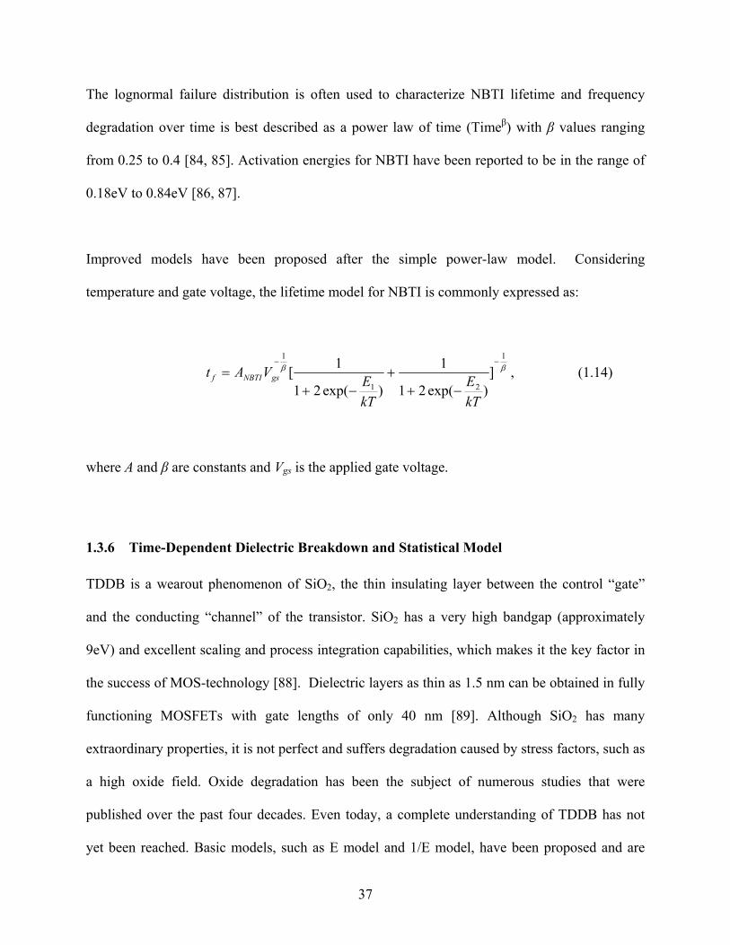
37
The lognormal failure distribution is often used to characterize NBTI lifetime and frequency
degradation over time is best described as a power law of time (Timeβ) with β values ranging
from 0.25 to 0.4 [84, 85]. Activation energies for NBTI have been reported to be in the range of
0.18eV to 0.84eV [86, 87].
Improved models have been proposed after the simple power-law model. Considering
temperature and gate voltage, the lifetime model for NBTI is commonly expressed as:
ββ1
21
1
])exp(21
1
)exp(21
1[−−
−++
−+=
kTE
kTEVAt gsNBTIf , (1.14)
where A and β are constants and Vgs is the applied gate voltage.
1.3.6 Time-Dependent Dielectric Breakdown and Statistical Model
TDDB is a wearout phenomenon of SiO2, the thin insulating layer between the control “gate”
and the conducting “channel” of the transistor. SiO2 has a very high bandgap (approximately
9eV) and excellent scaling and process integration capabilities, which makes it the key factor in
the success of MOS-technology [88]. Dielectric layers as thin as 1.5 nm can be obtained in fully
functioning MOSFETs with gate lengths of only 40 nm [89]. Although SiO2 has many
extraordinary properties, it is not perfect and suffers degradation caused by stress factors, such as
a high oxide field. Oxide degradation has been the subject of numerous studies that were
published over the past four decades. Even today, a complete understanding of TDDB has not
yet been reached. Basic models, such as E model and 1/E model, have been proposed and are
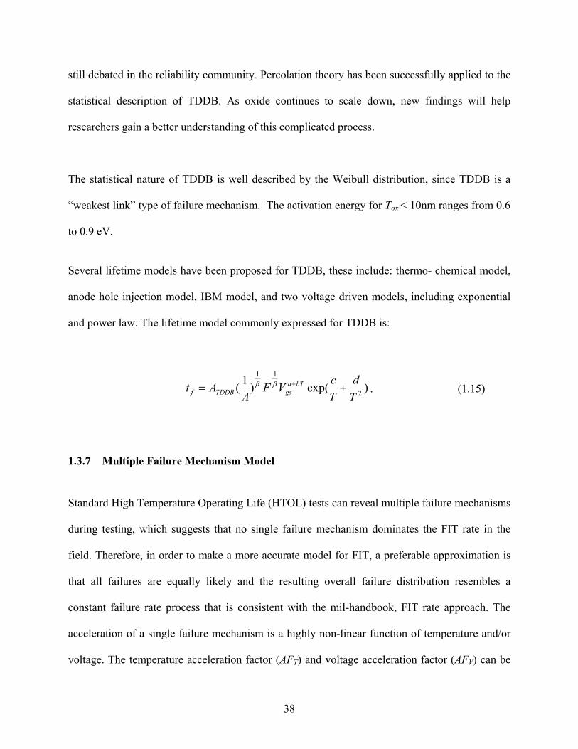
38
still debated in the reliability community. Percolation theory has been successfully applied to the
statistical description of TDDB. As oxide continues to scale down, new findings will help
researchers gain a better understanding of this complicated process.
The statistical nature of TDDB is well described by the Weibull distribution, since TDDB is a
“weakest link” type of failure mechanism. The activation energy for Tox < 10nm ranges from 0.6
to 0.9 eV.
Several lifetime models have been proposed for TDDB, these include: thermo- chemical model,
anode hole injection model, IBM model, and two voltage driven models, including exponential
and power law. The lifetime model commonly expressed for TDDB is:
)exp()1( 2
11
Td
TcVF
AAt bTa
gsTDDBf += +ββ . (1.15)
1.3.7 Multiple Failure Mechanism Model
Standard High Temperature Operating Life (HTOL) tests can reveal multiple failure mechanisms
during testing, which suggests that no single failure mechanism dominates the FIT rate in the
field. Therefore, in order to make a more accurate model for FIT, a preferable approximation is
that all failures are equally likely and the resulting overall failure distribution resembles a
constant failure rate process that is consistent with the mil-handbook, FIT rate approach. The
acceleration of a single failure mechanism is a highly non-linear function of temperature and/or
voltage. The temperature acceleration factor (AFT) and voltage acceleration factor (AFV) can be
39
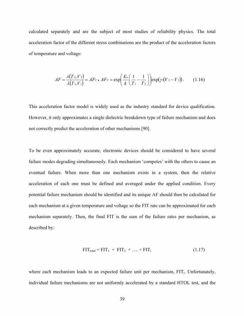
calculated separately and are the subject of most studies of reliability physics. The total
acceleration factor of the different stress combinations are the product of the acceleration factors
of temperature and voltage:
( )( ) ( )( )121
2111
22 exp11exp,, VV
TTkEAFAF
VTVTAF a
VT −⎟⎟⎠
⎞⎜⎜⎝
⎛⎟⎠⎞
⎜⎝⎛ −=== • γ
λλ . (1.16)
This acceleration factor model is widely used as the industry standard for device qualification.
However, it only approximates a single dielectric breakdown type of failure mechanism and does
not correctly predict the acceleration of other mechanisms [90].
To be even approximately accurate, electronic devices should be considered to have several
failure modes degrading simultaneously. Each mechanism ‘competes’ with the others to cause an
eventual failure. When more than one mechanism exists in a system, then the relative
acceleration of each one must be defined and averaged under the applied condition. Every
potential failure mechanism should be identified and its unique AF should then be calculated for
each mechanism at a given temperature and voltage so the FIT rate can be approximated for each
mechanism separately. Then, the final FIT is the sum of the failure rates per mechanism, as
described by:
FITtotal = FIT1 + FIT2 + …. + FITi (1.17)
where each mechanism leads to an expected failure unit per mechanism, FITi. Unfortunately,
individual failure mechanisms are not uniformly accelerated by a standard HTOL test, and the
40
manufacturer is forced to model a single acceleration factor that cannot be combined with known
physics of failure models [90].
1.3.8 Acceleration Factor
The qualification of device reliability, as reported by a FIT rate, must be based on an acceleration
factor, which represents the failure model for the tested device. If we assume that there is no
failure analysis (FA) of the devices after the HTOL test, or that the manufacturer does not report
FA results to the customer, then a model should be made for the acceleration factor, AF, based
on a combination of competing mechanisms [90].
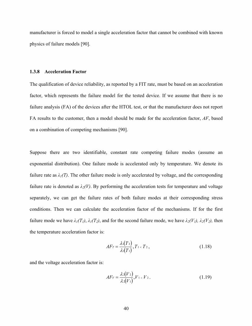
Suppose there are two identifiable, constant rate competing failure modes (assume an
exponential distribution). One failure mode is accelerated only by temperature. We denote its
failure rate as λ1(T). The other failure mode is only accelerated by voltage, and the corresponding
failure rate is denoted as λ2(V). By performing the acceleration tests for temperature and voltage
separately, we can get the failure rates of both failure modes at their corresponding stress
conditions. Then we can calculate the acceleration factor of the mechanisms. If for the first
failure mode we have λ1(T1), λ1(T2), and for the second failure mode, we have λ2(V1), λ2(V2), then
the temperature acceleration factor is:
( )( ) 21
11
21 , TTTTAFT <=
λλ , (1.18)
and the voltage acceleration factor is:
( )( ) 21
12
22 , VVVVAFV <=
λλ . (1.19)
41
The system acceleration factor between the stress conditions of (T1,V1) and (T2,V2) is:
( ) ( )( ) ( )
( ) ( )( ) ( )1211
2221
112111
222221
,,,,
VTVT
VTVTVTVTAF
λλλλ
λλλλ
++
++
= = . (1.20)
The above equation can be transformed to the following two expressions:
( ) ( )( ) ( )
VT AFV
AFT
VTAF2221
2221
λλλλ
+
+= , (1.21)
or
( ) ( )( ) ( )1211
1211
VTAFVAFTAF VT
λλλλ
++
= . (1.22)
These two equations can be simplified based on different assumptions. When λ1(T1) = λ2(V1)
where there is an equal probability under normal operating conditions:
2VT AFAFAF +
= . (1.23)
Therefore, unless the temperature and voltage is carefully chosen so that AFT and AFV are very
close, within a factor of about 2, then one acceleration factor will overwhelm the failures at the
accelerated conditions. Similarly, when λ1(T2) = λ2(V2) i.e., an equal probability during
accelerated test condition, then the AF will take the form:
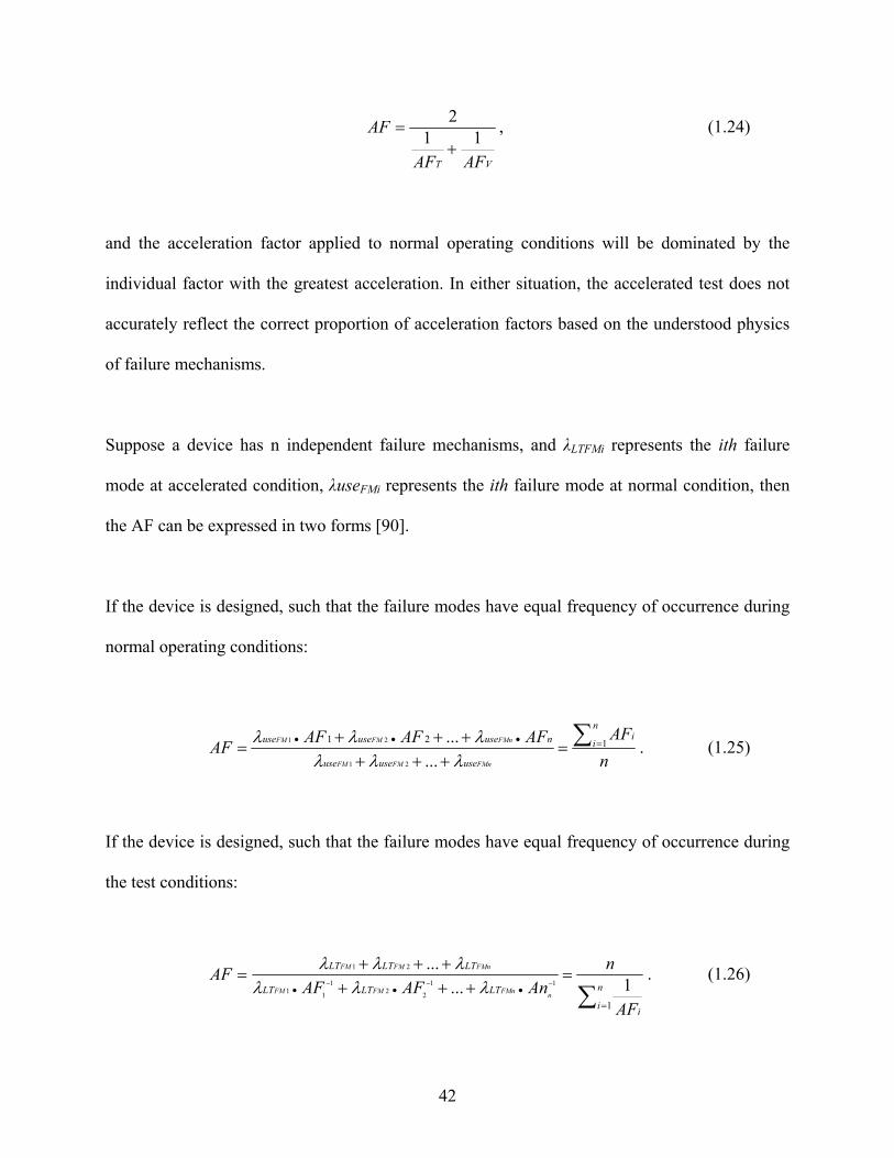
42
VT AFAF
AF 112
+= , (1.24)
and the acceleration factor applied to normal operating conditions will be dominated by the
individual factor with the greatest acceleration. In either situation, the accelerated test does not
accurately reflect the correct proportion of acceleration factors based on the understood physics
of failure mechanisms.
Suppose a device has n independent failure mechanisms, and λLTFMi represents the ith failure
mode at accelerated condition, λuseFMi represents the ith failure mode at normal condition, then
the AF can be expressed in two forms [90].
If the device is designed, such that the failure modes have equal frequency of occurrence during
normal operating conditions:
nAFAFAFAFAF
n
ii
useuseuse
nuseuseuse
FMnFMFM
FMnFMFM ∑ =•••=
++++++
= 121
......
21
21
λλλλλλ . (1.25)
If the device is designed, such that the failure modes have equal frequency of occurrence during
the test conditions:
∑ =•••
=+++
+++=
−−− n
i i
LTLTLT
LTLTLT
AF
nAnAFAF
AFnFMnFMFM
FMnFMFM
1
1......
11
221
11
21
λλλλλλ . (1.26)
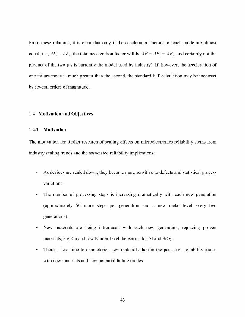
43
From these relations, it is clear that only if the acceleration factors for each mode are almost
equal, i.e., AF1 ~ AF2, the total acceleration factor will be AF = AF1 = AF2, and certainly not the
product of the two (as is currently the model used by industry). If, however, the acceleration of
one failure mode is much greater than the second, the standard FIT calculation may be incorrect
by several orders of magnitude.
1.4 Motivation and Objectives
1.4.1 Motivation
The motivation for further research of scaling effects on microelectronics reliability stems from
industry scaling trends and the associated reliability implications:
• As devices are scaled down, they become more sensitive to defects and statistical process
variations.
• The number of processing steps is increasing dramatically with each new generation
(approximately 50 more steps per generation and a new metal level every two
generations).
• New materials are being introduced with each new generation, replacing proven
materials, e.g. Cu and low K inter-level dielectrics for Al and SiO2.
• There is less time to characterize new materials than in the past, e.g., reliability issues
with new materials and new potential failure modes.
44
• Manufacturers are trending toward providing ‘just enough’ lifetime, reliability, and
environmental specifications for commercial applications, e.g., < five year product
lifetimes, trading off ‘excess’ reliability margins for performance.
• There is a significant rise in the amount of proprietary technology and data developed by
manufacturers, and there is a reluctance to share that information with hi-rel customers,
e.g., process recipes, process controls, process flows, design margins, MTTF.
• There is a focus on the commercial customer, with little or no emphasis on the needs of
the space customer, e.g., extended life, extreme environments, high reliability.
• There are increasingly difficult testability challenges due to part complexity.
Modern reliability approaches, including a PoF based reliability modeling strategy, are needed to
better predict long term product reliability, operating margins, and performance of progressively
scaled technologies in NASA applications. NASA and other hi-rel users must be able to reliably
predict end-of-life characteristics and time-to-failure of these advanced scaled technologies for
the next generation of flight avionics systems. Further research, modeling, accelerated testing,
and failure analysis are needed to better understand the impact of nanometer semiconductor
scaling on microelectronics reliability. The relationship between smaller technology feature
sizes, device failure mechanisms, and activation energies must be further investigated to
quantifiably assess the reliability of current microelectronic products across different stress
conditions for hi-rel NASA space applications. Better predictive models explaining the
anticipated behavior of advanced scaled microelectronic technologies, and the expected
performance degradation over time are desired. Physics-of-failure derating guidance for
advanced scaled microelectronics is needed. A qualification plan, based upon analysis from
45
testing at multiple stress conditions and the failure mechanism process rates, is sought after to
better design for high reliability and long life.
While earlier AVSI sponsored work has produced some of the empirical models needed for a
PoF based derating approach, and better simulation models have been developed to predict
device wearout under various stress conditions, experimental verification and validation of the
outputs of these models continues. This work will include a series of experiments to evaluate
some of the more recent memory technologies to substantiate and validate proposed acceleration
models for temperature and voltage life-stress relationships across scaled technologies. The
purpose of this work is to develop a better understanding of the impact of nanometer technology
scaling on microelectronics reliability, assess current trends, and provide an independent
assessment of some of the proposed acceleration models so that we are able to better predict the
reliability of scaled microelectronic technologies in hi-rel systems, and eventually apply PoF
based derating models.
Empirical and computer-based modeling, simulation, and analyses are being employed to build
PoF based FR estimation models to assess the impact of various failure mechanisms on product
reliability, and extrapolate bathtub curves across progressively technologies, e.g., 180nm,
130nm, 110nm, and 90nm. This work may lead to more accurate prediction of device life given
a range of mission operating conditions, and may become particularly beneficial for predicting
device life of progressive technologies outside of normal operating conditions. It is the goal of
this work to investigate and validate reliability trends as a function of technology scaling by
conducting independent accelerated stress testing at the product level, data analysis of the results,
46
modeling, and failure analysis of several scaled device technologies. Testing at multiple
conditions to quantify the rate processes of different failure mechanisms will be attempted.
Memory devices are excellent choices for product reliability experimentation because of their
high density of transistors, memory cells, and repetitive layout of memory blocks. Current
SDRAM products are available in >512Mb density per semiconductor chip.
Predicting long-term performance of scaled microelectronic memory products can be difficult
because ALT involving elevated stresses can often result in either too few or no failures to make
realistic predictions or inferences. It is also possible to overstress the part during accelerated
stress testing to the point of thermal runaway where the device goes into catastrophic failure.
Manufacturers often report product FIT rates based on zero failures over a fixed amount of time.
To overcome this problem, ADT can be used as a means to predict performance in such cases.
By identifying key performance measures which are expected to degrade over time, product
reliability can be inferred by the degradation paths without observing actual physical failures.
Using this approach, the engineer defines a failure as the first time a key performance measure
exceeds a pre-specified threshold and the degradation path is then correlated to product
reliability. Manufacturers will develop specification minimum and maximum limits on key
operating parameters for their products and establish acceptable ranges for key characteristics.
Through internal process controls and reliability and qualification testing, manufacturers will
create acceptable parameter limits to achieve a target reliability FIT. Often times, however, the
user does not have access to the actual failure data, failure distribution or confidence level
bounds for a given product.
47
1.4.2 Objectives
The main objectives of the research are to: test, analyze, and model competing intrinsic failure
mechanisms of scaled microelectronic products involving both hard catastrophic and soft
degradation failures under accelerated conditions; validate existing models and/or propose new
models describing wearout and performance degradation of several scaled technologies from the
experimental baseline; and develop conclusions and predictions of the expected failure rate of
the next product generation.
48
Chapter 2: Scaling Impact on SDRAM
2.1 Overview
Dynamic RAM is a type of volatile memory that needs to be periodically refreshed to retain its
contents. SDRAM has a synchronous interface, meaning that it waits for a clock signal before
responding to its control inputs. It is synchronized with the computer's system bus, and thus with
the processor. DRAM is the most common kind of random access memory for personal
computers, workstations and flight computers, such as the one that will be used in the upcoming
NASA JUNO mission. DRAMs use charge storage on a capacitor in each memory cell to
represent stored binary data values of a logic “1” or a logic “0”. A DRAM cell consists of a
transfer device, a MOSFET that acts like a switch and a storage capacitor as is displayed in
Figure 10 [99]. The absence of a charge on the capacitor represents a logic “0” and the presence
of a charge indicates a logic “1” in each memory cell. Millions of these memory cells are
populated in high density arrays.
The clock is used to drive an internal finite state machine that pipelines incoming instructions.
This allows the chip to have a more complex pattern of operation than DRAM which does not
have synchronizing control circuits. Pipelining means that the chip can accept a new instruction
before it has finished processing the previous one. In a pipelined write, the write command can
be immediately followed by another instruction without waiting for the data to be written to the
memory array. In a pipelined read, the requested data appears after a fixed number of clock
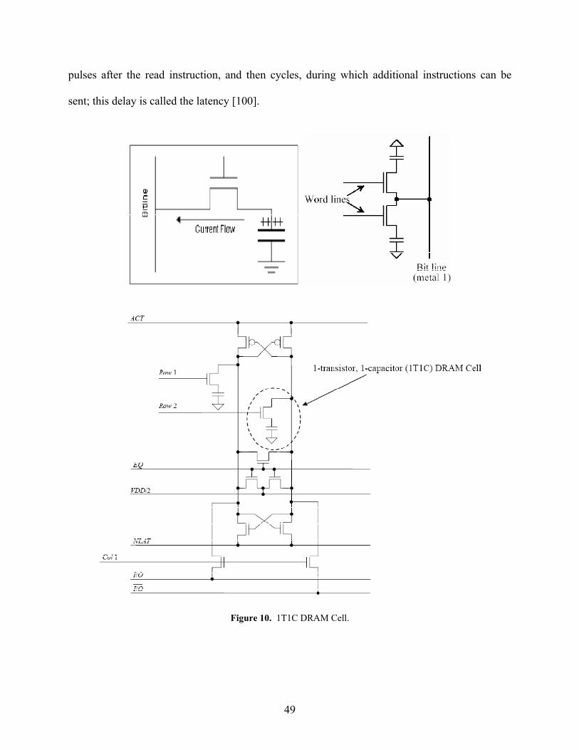
49
pulses after the read instruction, and then cycles, during which additional instructions can be
sent; this delay is called the latency [100].
Figure 10. 1T1C DRAM Cell.
50
While the access latency of DRAM is fundamentally limited by the DRAM array, DRAM has
very high potential bandwidth because each internal read is actually a row of many thousands of
bits. To make more of this bandwidth available to users, a Double Data Rate (DDR) interface
was developed. This uses the same commands, accepted once per cycle, but reads or writes two
words of data per clock cycle. Some minor changes to the Single Data Rate (SDR) interface
timing were made and the supply voltage was reduced from 3.3 to 2.5 V. DDR SDRAM (also
called "DDR1") doubles the minimum read or write unit; every access refers to at least two
consecutive words. DDR2 SDRAM was originally seen as a minor enhancement based on the
industry standard single-core CPU on DDR1 SDRAM. It mainly allowed higher clock speeds
and somewhat deeper pipelining better suited for the rapid acceptance of the multi-core CPU in
2006. With the development and introduction of DDR3 SDRAM in 2007, it is anticipated that
DDR3 will quickly replace the more limited DDR and newer DDR2 in cutting edge multi-core
CPU architectures. The popularity of DRAM for such applications as PCs, wireless access, MP3
players, digital televisions and DVD video recorders makes this type of memory a leading
technology driver, with ever increasing pressure to reduce cost per bit with higher densities.
DRAM makes up over 50% of the embedded memory market. Figures 11a-c display current
commercial DRAM trends [101].
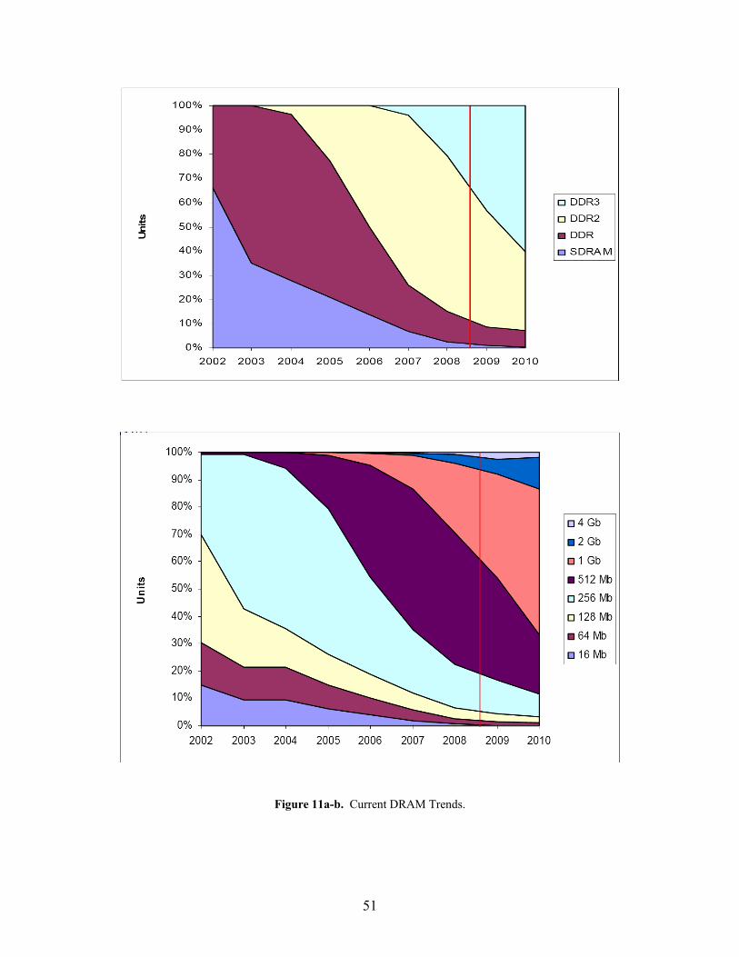
51
Figure 11a-b. Current DRAM Trends.
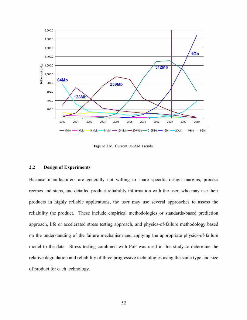
52
Figure 11c. Current DRAM Trends.
2.2 Design of Experiments
Because manufacturers are generally not willing to share specific design margins, process
recipes and steps, and detailed product reliability information with the user, who may use their
products in highly reliable applications, the user may use several approaches to assess the
reliability the product. These include empirical methodologies or standards-based prediction
approach, life or accelerated stress testing approach, and physics-of-failure methodology based
on the understanding of the failure mechanism and applying the appropriate physics-of-failure
model to the data. Stress testing combined with PoF was used in this study to determine the
relative degradation and reliability of three progressive technologies using the same type and size
of product for each technology.
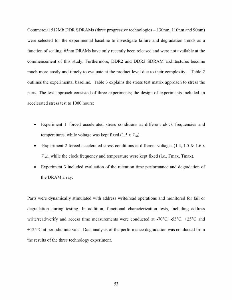
53
Commercial 512Mb DDR SDRAMs (three progressive technologies – 130nm, 110nm and 90nm)
were selected for the experimental baseline to investigate failure and degradation trends as a
function of scaling. 65nm DRAMs have only recently been released and were not available at the
commencement of this study. Furthermore, DDR2 and DDR3 SDRAM architectures become
much more costly and timely to evaluate at the product level due to their complexity. Table 2
outlines the experimental baseline. Table 3 explains the stress test matrix approach to stress the
parts. The test approach consisted of three experiments; the design of experiments included an
accelerated stress test to 1000 hours:
• Experiment 1 forced accelerated stress conditions at different clock frequencies and
temperatures, while voltage was kept fixed (1.5 x Vdd).
• Experiment 2 forced accelerated stress conditions at different voltages (1.4, 1.5 & 1.6 x
Vdd), while the clock frequency and temperature were kept fixed (i.e., Fmax, Tmax).
• Experiment 3 included evaluation of the retention time performance and degradation of
the DRAM array.
Parts were dynamically stimulated with address write/read operations and monitored for fail or
degradation during testing. In addition, functional characterization tests, including address
write/read/verify and access time measurements were conducted at -70°C, -55°C, +25°C and
+125°C at periodic intervals. Data analysis of the performance degradation was conducted from
the results of the three technology experiment.
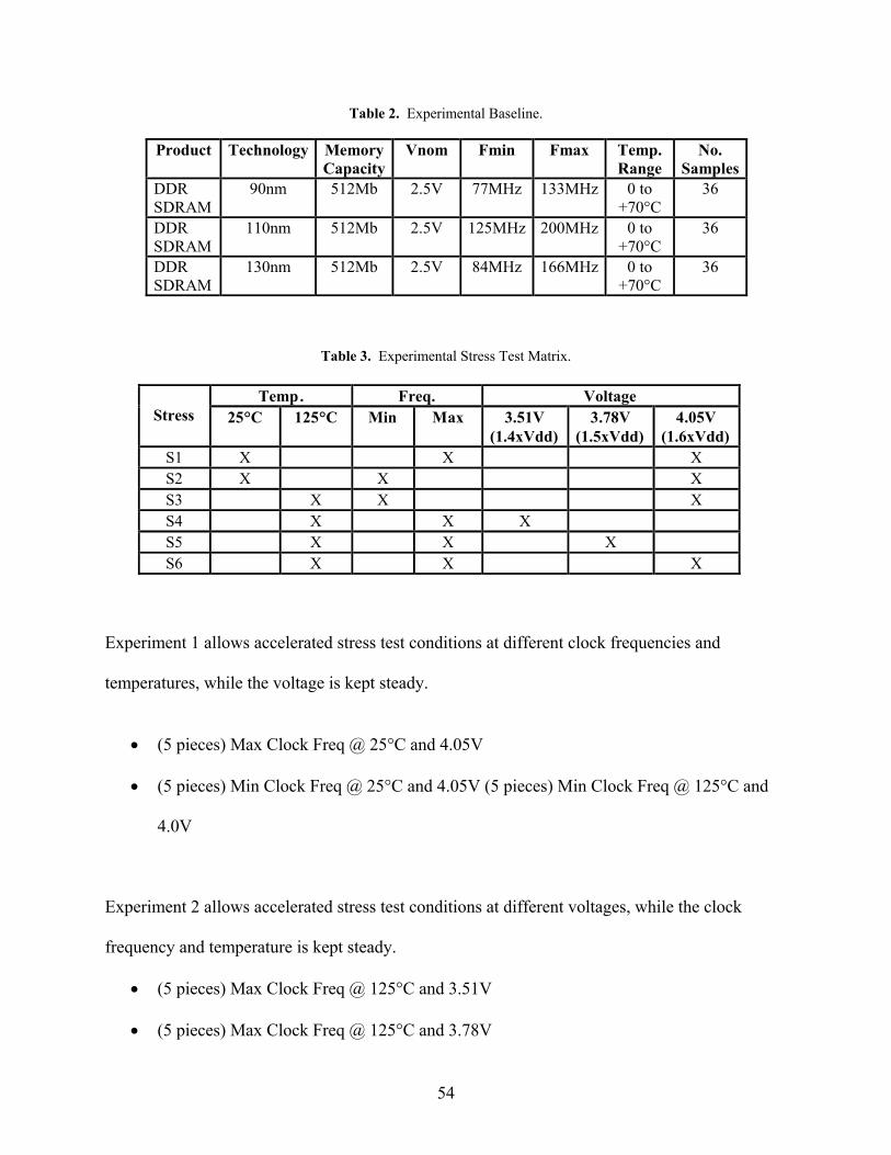
54
Table 2. Experimental Baseline.
Table 3. Experimental Stress Test Matrix.
Experiment 1 allows accelerated stress test conditions at different clock frequencies and
temperatures, while the voltage is kept steady.
• (5 pieces) Max Clock Freq @ 25°C and 4.05V
• (5 pieces) Min Clock Freq @ 25°C and 4.05V (5 pieces) Min Clock Freq @ 125°C and
4.0V
Experiment 2 allows accelerated stress test conditions at different voltages, while the clock
frequency and temperature is kept steady.
• (5 pieces) Max Clock Freq @ 125°C and 3.51V
• (5 pieces) Max Clock Freq @ 125°C and 3.78V
Product Technology Memory Capacity
Vnom Fmin Fmax
Temp. Range
No. Samples
DDR SDRAM
90nm 512Mb 2.5V 77MHz 133MHz 0 to +70°C
36
DDR SDRAM
110nm 512Mb 2.5V 125MHz 200MHz 0 to +70°C
36
DDR SDRAM
130nm 512Mb 2.5V 84MHz 166MHz 0 to +70°C
36
Temp . Freq. Voltage Stress 25 °C 125 °C Min Max 3.51V
(1.4xVdd) 3.78V
(1.5xVdd) 4 .05V
(1.6xVdd) S1 X X X S2 X X X S3 X X X S4 X X X S5 X X X S6 X X X
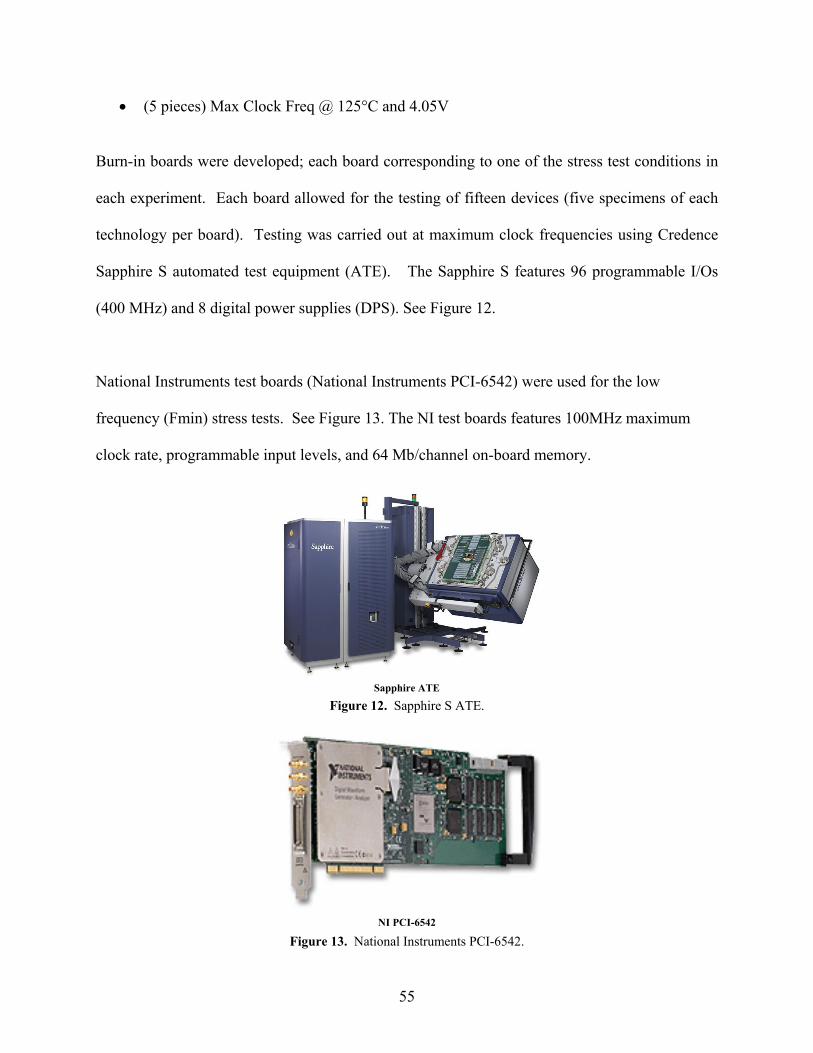
55
• (5 pieces) Max Clock Freq @ 125°C and 4.05V
Burn-in boards were developed; each board corresponding to one of the stress test conditions in
each experiment. Each board allowed for the testing of fifteen devices (five specimens of each
technology per board). Testing was carried out at maximum clock frequencies using Credence
Sapphire S automated test equipment (ATE). The Sapphire S features 96 programmable I/Os
(400 MHz) and 8 digital power supplies (DPS). See Figure 12.
National Instruments test boards (National Instruments PCI-6542) were used for the low
frequency (Fmin) stress tests. See Figure 13. The NI test boards features 100MHz maximum
clock rate, programmable input levels, and 64 Mb/channel on-board memory.
Sapphire ATE
Figure 12. Sapphire S ATE.
NI PCI-6542
Figure 13. National Instruments PCI-6542.
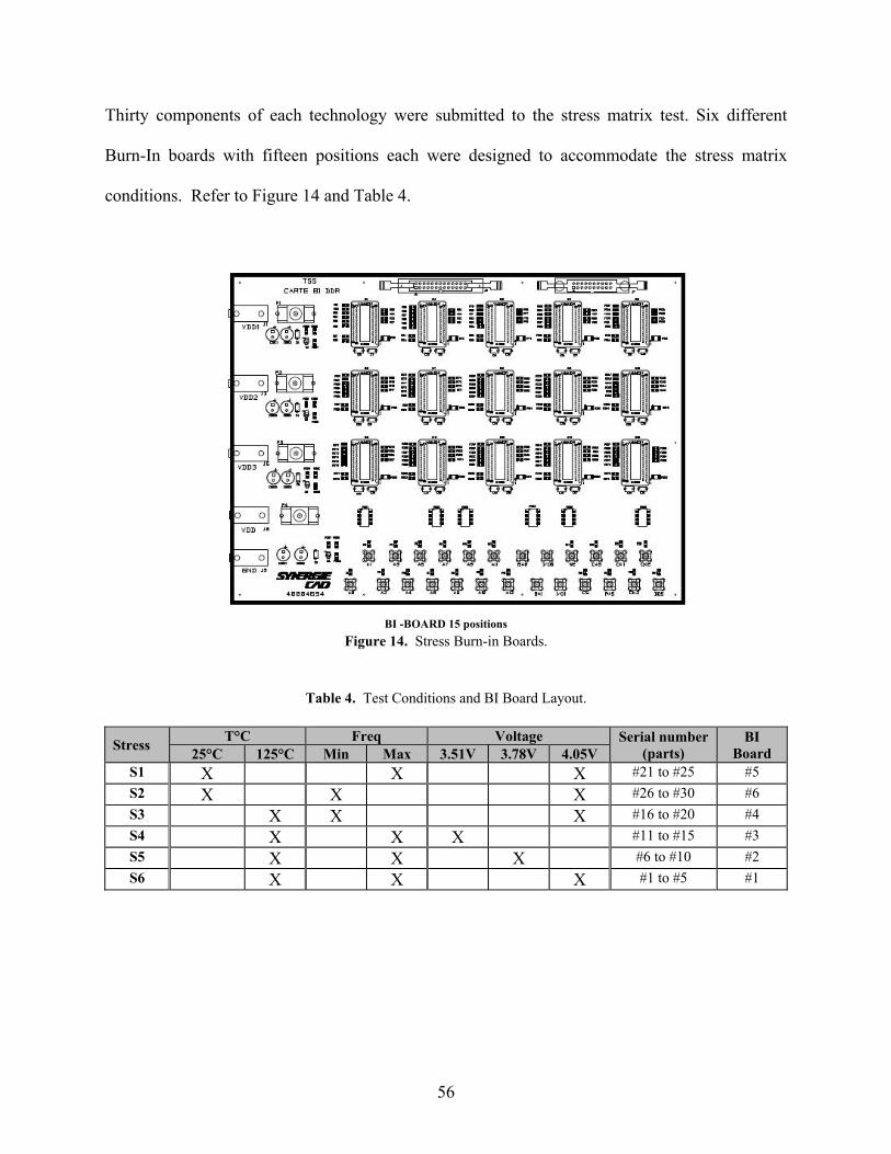
56
Thirty components of each technology were submitted to the stress matrix test. Six different
Burn-In boards with fifteen positions each were designed to accommodate the stress matrix
conditions. Refer to Figure 14 and Table 4.
BI -BOARD 15 positions Figure 14. Stress Burn-in Boards.
Table 4. Test Conditions and BI Board Layout.
Stress T°C Freq Voltage Serial number (parts)
BI Board 25°C 125°C Min Max 3.51V 3.78V 4.05V
S1 X X X #21 to #25 #5 S2 X X X #26 to #30 #6 S3 X X X #16 to #20 #4 S4 X X X #11 to #15 #3 S5 X X X #6 to #10 #2 S6 X X X #1 to #5 #1

57
2.2.1 Electrical Test Flow
For each memory device, electrical test software and hardware were developed. Tests were
performed using an EXA 3000 digital tester. At each electrical test step the following tests were
conducted:
DC Tests:
• Continuity Tests (Vfwd).
• Input leakage current test (IiL/IiH).
• Output leakage current test (IozL/IozH).
• Low/High output current (IoL/IoH).
• Operating current (ACT-PRE) (Iddo0).
• Operating current (ACT-READ-PRE) (Iddo1).
• Idle power down standby current (Iddo2P).
• Floating idle standby current (Iddo2F).
• Active power down standby current (Iddo3P).
• Active standby current (Iddo3N).
• Operating current (Burst Read Operation) (Iddo4R).
• Operating current (Burst Write Operation) (Iddo4W).
• Auto-Refresh Burst Current (Iddo5).
• Self refresh current (Iddo6).
• Operating current (4 banks interleaving) (Iddo7).
Functional Tests:
• Functional test at 133MHz and nominal Vdd .
58
• Functional test at 133MHz and minimum Vdd .
• Functional test at 133MHz and maximum Vdd .
Dynamic Tests:
• DQ output access time from CK, CK/ (tAC).
2.2.2 Electrical Test Conditions and Limits
The electrical test conditions, limits and patterns for each parameter are described in Table 5
where:
Device D1 (90nm): 512Mb DDR SDRAM
Device D2 (110nm): 512Mb DDR SDRAM
Device D3 (130nm): 512Mb DDR SDRAM
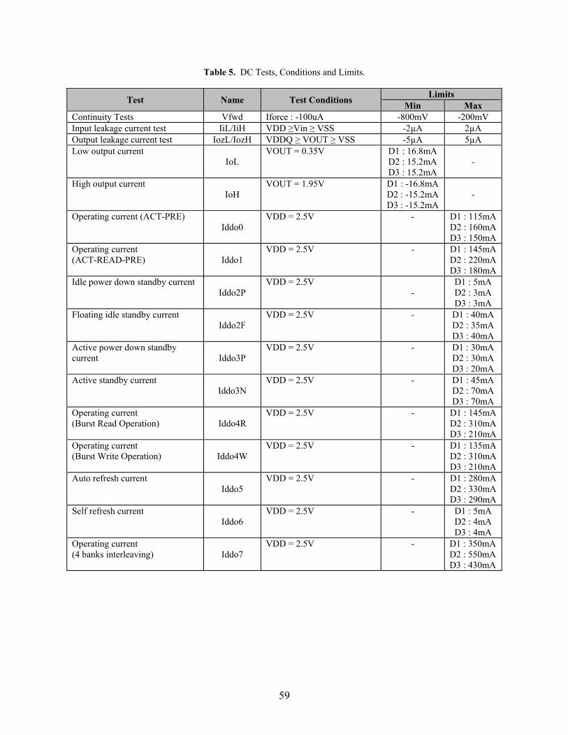
59
Table 5. DC Tests, Conditions and Limits.
Test Name Test Conditions Limits Min Max
Continuity Tests Vfwd Iforce : -100uA -800mV -200mV Input leakage current test IiL/IiH VDD ≥Vin ≥ VSS -2µA 2µA Output leakage current test IozL/IozH VDDQ ≥ VOUT ≥ VSS -5µA 5µA Low output current
IoL VOUT = 0.35V D1 : 16.8mA
D2 : 15.2mA D3 : 15.2mA
-
High output current IoH
VOUT = 1.95V D1 : -16.8mA D2 : -15.2mA D3 : -15.2mA
-
Operating current (ACT-PRE) Iddo0
VDD = 2.5V - D1 : 115mA D2 : 160mA D3 : 150mA
Operating current (ACT-READ-PRE) Iddo1
VDD = 2.5V - D1 : 145mA D2 : 220mA D3 : 180mA
Idle power down standby current Iddo2P
VDD = 2.5V -
D1 : 5mA D2 : 3mA D3 : 3mA
Floating idle standby current Iddo2F
VDD = 2.5V - D1 : 40mA D2 : 35mA D3 : 40mA
Active power down standby current Iddo3P
VDD = 2.5V - D1 : 30mA D2 : 30mA D3 : 20mA
Active standby current Iddo3N
VDD = 2.5V - D1 : 45mA D2 : 70mA D3 : 70mA
Operating current (Burst Read Operation) Iddo4R
VDD = 2.5V - D1 : 145mA D2 : 310mA D3 : 210mA
Operating current (Burst Write Operation) Iddo4W
VDD = 2.5V - D1 : 135mA D2 : 310mA D3 : 210mA
Auto refresh current Iddo5
VDD = 2.5V - D1 : 280mA D2 : 330mA D3 : 290mA
Self refresh current Iddo6
VDD = 2.5V - D1 : 5mA D2 : 4mA D3 : 4mA
Operating current (4 banks interleaving) Iddo7
VDD = 2.5V - D1 : 350mA D2 : 550mA D3 : 430mA
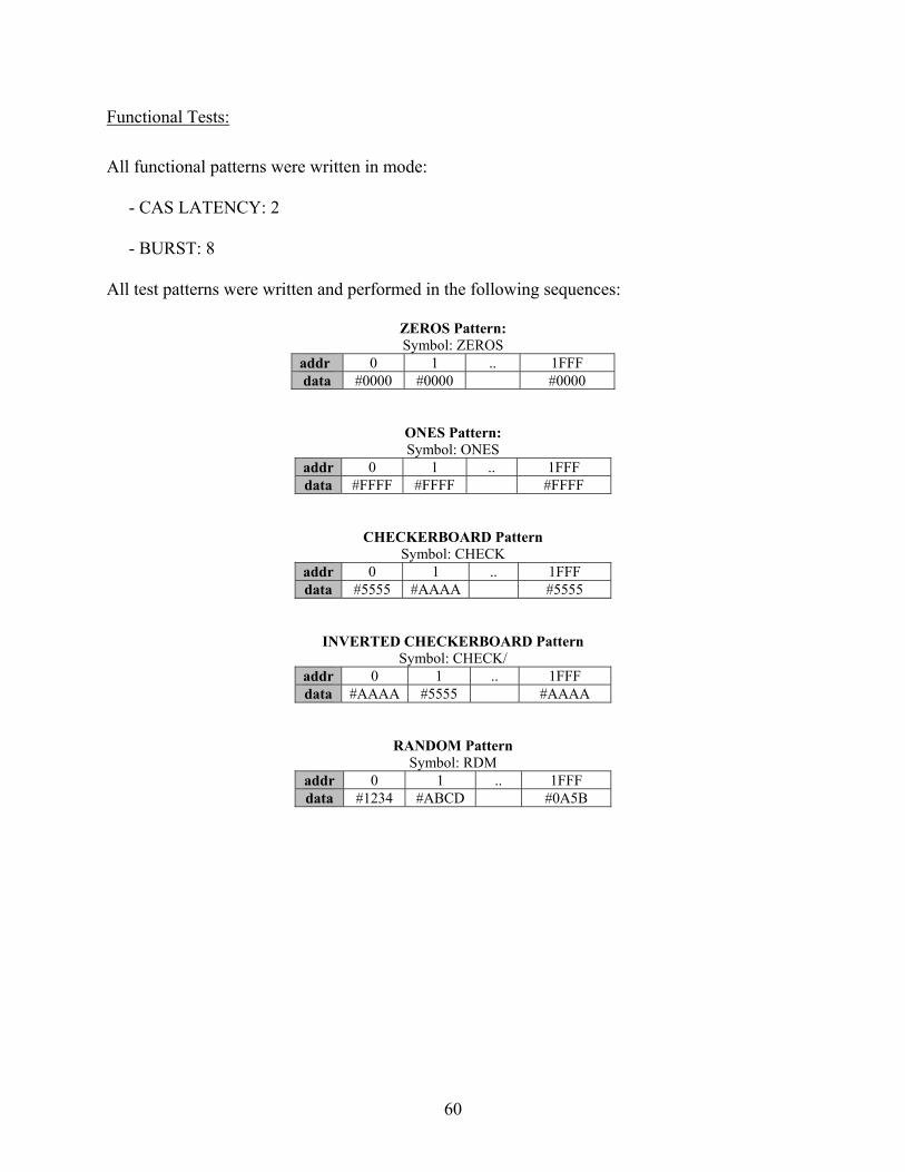
60
Functional Tests:
All functional patterns were written in mode:
- CAS LATENCY: 2
- BURST: 8
All test patterns were written and performed in the following sequences:
ZEROS Pattern: Symbol: ZEROS
addr 0 1 .. 1FFF data #0000 #0000 #0000
ONES Pattern: Symbol: ONES
addr 0 1 .. 1FFF data #FFFF #FFFF #FFFF
CHECKERBOARD Pattern Symbol: CHECK
addr 0 1 .. 1FFF data #5555 #AAAA #5555
INVERTED CHECKERBOARD Pattern Symbol: CHECK/
addr 0 1 .. 1FFF data #AAAA #5555 #AAAA
RANDOM Pattern Symbol: RDM
addr 0 1 .. 1FFF data #1234 #ABCD #0A5B
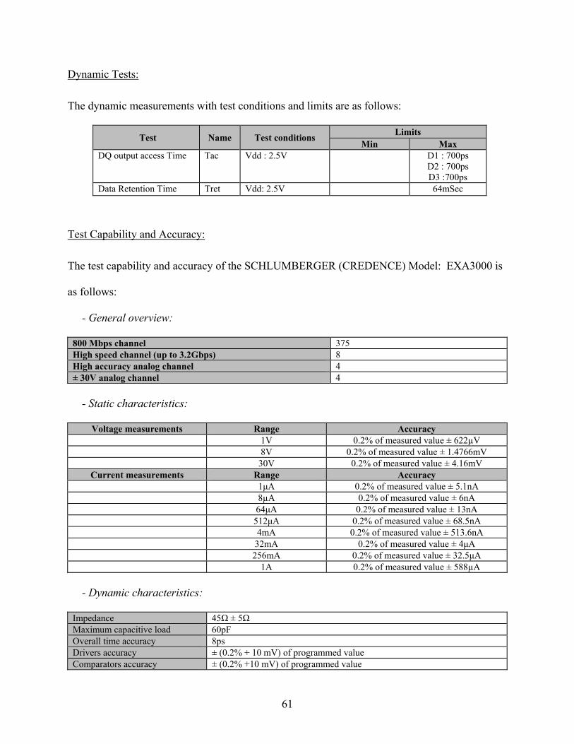
61
Dynamic Tests:
The dynamic measurements with test conditions and limits are as follows:
Test Name Test conditions Limits Min Max
DQ output access Time Tac Vdd : 2.5V D1 : 700ps D2 : 700ps D3 :700ps
Data Retention Time Tret Vdd: 2.5V 64mSec
Test Capability and Accuracy:
The test capability and accuracy of the SCHLUMBERGER (CREDENCE) Model: EXA3000 is
as follows:
- General overview:
800 Mbps channel 375 High speed channel (up to 3.2Gbps) 8 High accuracy analog channel 4 ± 30V analog channel 4
- Static characteristics:
Voltage measurements Range Accuracy
1V 0.2% of measured value ± 622µV 8V 0.2% of measured value ± 1.4766mV 30V 0.2% of measured value ± 4.16mV
Current measurements Range Accuracy 1μA 0.2% of measured value ± 5.1nA 8µA 0.2% of measured value ± 6nA 64μA 0.2% of measured value ± 13nA 512μA 0.2% of measured value ± 68.5nA 4mA 0.2% of measured value ± 513.6nA 32mA 0.2% of measured value ± 4μA 256mA 0.2% of measured value ± 32.5μA 1A 0.2% of measured value ± 588µA
- Dynamic characteristics:
Impedance 45Ω ± 5Ω Maximum capacitive load 60pF Overall time accuracy 8ps Drivers accuracy ± (0.2% + 10 mV) of programmed value Comparators accuracy ± (0.2% +10 mV) of programmed value
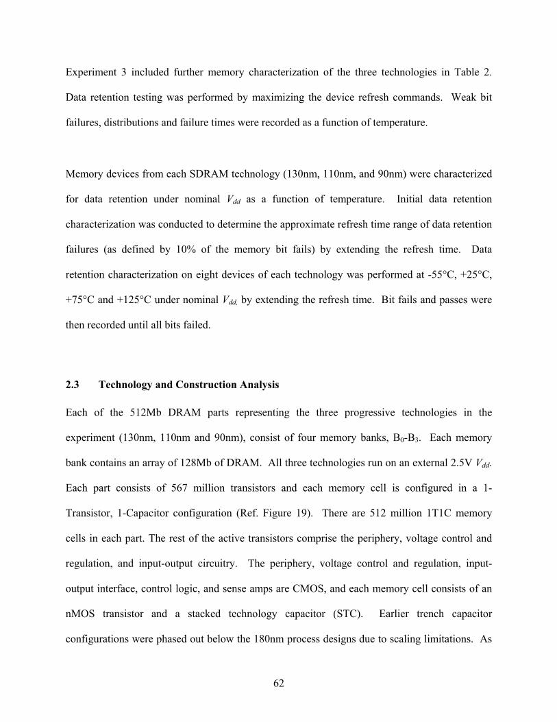
62
Experiment 3 included further memory characterization of the three technologies in Table 2.
Data retention testing was performed by maximizing the device refresh commands. Weak bit
failures, distributions and failure times were recorded as a function of temperature.
Memory devices from each SDRAM technology (130nm, 110nm, and 90nm) were characterized
for data retention under nominal Vdd as a function of temperature. Initial data retention
characterization was conducted to determine the approximate refresh time range of data retention
failures (as defined by 10% of the memory bit fails) by extending the refresh time. Data
retention characterization on eight devices of each technology was performed at -55°C, +25°C,
+75°C and +125°C under nominal Vdd, by extending the refresh time. Bit fails and passes were
then recorded until all bits failed.
2.3 Technology and Construction Analysis Each of the 512Mb DRAM parts representing the three progressive technologies in the
experiment (130nm, 110nm and 90nm), consist of four memory banks, B0-B3. Each memory
bank contains an array of 128Mb of DRAM. All three technologies run on an external 2.5V Vdd.
Each part consists of 567 million transistors and each memory cell is configured in a 1-
Transistor, 1-Capacitor configuration (Ref. Figure 19). There are 512 million 1T1C memory
cells in each part. The rest of the active transistors comprise the periphery, voltage control and
regulation, and input-output circuitry. The periphery, voltage control and regulation, input-
output interface, control logic, and sense amps are CMOS, and each memory cell consists of an
nMOS transistor and a stacked technology capacitor (STC). Earlier trench capacitor
configurations were phased out below the 180nm process designs due to scaling limitations. As

63
DRAM has scaled down, the amount of charge needed for reliable memory operation has
basically remained the same. For current generation DRAM, the capacitance is typically 30-
40fF/cell. Although the external power supply is 2.5V for each part, internal on-chip voltage
regulator circuitry subdivides this voltage as follows:
130nm Technology Parts:
- Peripheral Circuitry Voltage: 2.2V
- Memory Core Voltage: 1.8V
110nm Technology Parts:
- Peripheral Circuitry Voltage: 1.8V
- Memory Core Voltage: 1.4V
90nm Technology Parts:
- Peripheral Circuitry Voltage: 1.4V
- Memory Core Voltage: 1.0V
The memory cell capacitor dielectric material of the parts is Ta2O5. The gate oxide thickness for
the larger peripheral circuitry transistors is approximately 7nm, and the gate oxide thickness for
the nMOS memory cell transistors is approximately 4.2 nm.
A basic functional block diagram of the 512Mb SDRAM is shown if Figure 15 [102].
64
Figure 15. 512Mb SDRAM Functional Block Diagram.
2.4 Device Characterization
2.4.1 Voltage Breakdown
Two devices from each technology were used for voltage breakdown characterization to
determine the point of breakdown. The following approach was used to characterize the
breakdown voltage:
Ramp Vdd from 2.7V to 8V
- Continuity I/O test
- Continuity Vdd /VddQ test
- Measure Standby Idd
65
For the three technologies, the breakdown voltage was higher than 6V for each of the 2.5V
nominal parts (130nm, 110 and 90nm). The 110nm and 130nm samples exhibited breakdown at
>7V.
2.4.2 Minimum Frequency Operation Characterization
Two devices from each technology were used to determine the actual minimum operating
frequency for each technology. Devices were electrically tested at 125°C to determine the
breakdown voltage for each technology (high temperature, ramp voltage to device breakdown).
All three technologies remained functional to 50MHz and the 130nm and 110nm parts remained
functional to 25MHz, well below the specified minimum operating frequency. The low
frequency used for electrical stress in the experimentation, Fmin, was 50MHz.
2.5 Stress Test Results
Most importantly, there were no hard functional failures of any of the devices after being
subjected to the stress conditions in experiments one and two. Although there were no failures
from the stress conditions applied from the stress test matrix, Iddo degradation was observed on
some parameters after 1,000 hours. Analyses of the results indicate the following parameters
were most affected by the stress conditions:
• Operating current: Iddo0
• Auto refresh current : Iddo5
• Data Retention Time: Tret
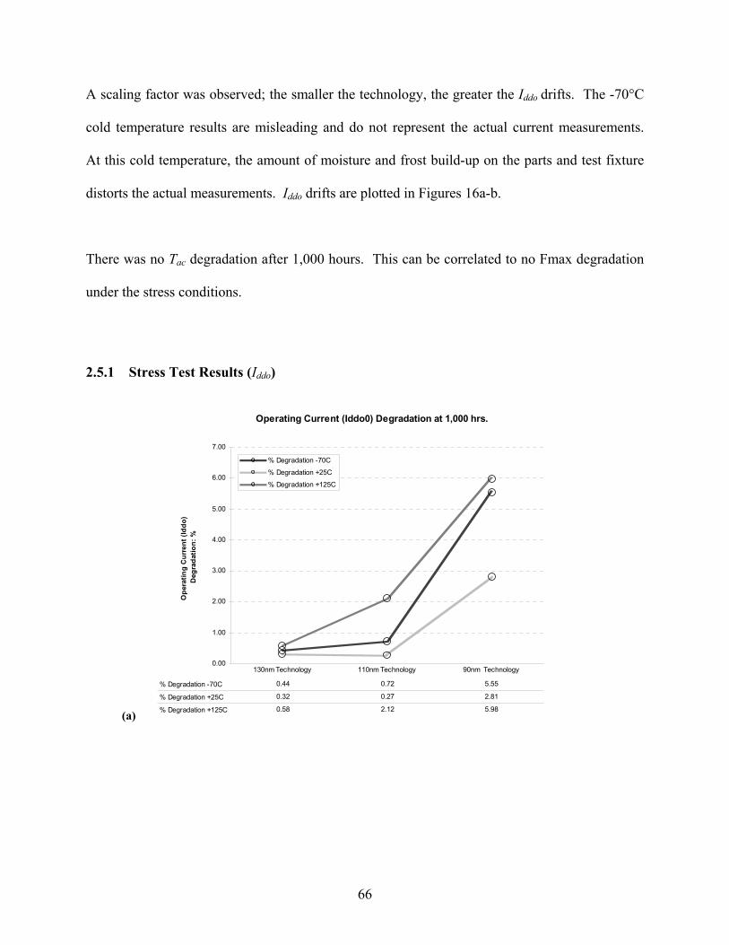
66
A scaling factor was observed; the smaller the technology, the greater the Iddo drifts. The -70°C
cold temperature results are misleading and do not represent the actual current measurements.
At this cold temperature, the amount of moisture and frost build-up on the parts and test fixture
distorts the actual measurements. Iddo drifts are plotted in Figures 16a-b.
There was no Tac degradation after 1,000 hours. This can be correlated to no Fmax degradation
under the stress conditions.
2.5.1 Stress Test Results (Iddo)
(a)
Operating Current (Iddo0) Degradation at 1,000 hrs.
0.00
1.00
2.00
3.00
4.00
5.00
6.00
7.00
Ope
ratin
g C
urre
nt (I
ddo)
D
egra
datio
n: %
% Degradation -70C
% Degradation +25C
% Degradation +125C
% Degradation -70C 0.44 0.72 5.55
% Degradation +25C 0.32 0.27 2.81
% Degradation +125C 0.58 2.12 5.98
130nm Technology 110nm Technology 90nm Technology
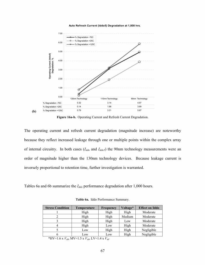
67
(b) Figure 16a-b. Operating Current and Refresh Current Degradation.
The operating current and refresh current degradation (magnitude increase) are noteworthy
because they reflect increased leakage through one or multiple points within the complex array
of internal circuitry. In both cases (Iddo and Iddo5) the 90nm technology measurements were an
order of magnitude higher than the 130nm technology devices. Because leakage current is
inversely proportional to retention time, further investigation is warranted.
Tables 6a and 6b summarize the Iddo performance degradation after 1,000 hours.
Table 6a. Iddo Performance Summary.
Stress Condition Temperature Frequency Voltage* Effect on Iddo 1 High High High Moderate 2 High High Medium Moderate 3 High High Low Moderate 4 High Low High Moderate 5 Low High High Negligible 6 Low Low High Negligible
*HV=1.6 x Vdd, MV=1.5 x Vdd, LV=1.4 x Vdd
Auto Refresh Current (Iddo5) Degradation at 1,000 hrs.
0.00
1.00
2.00
3.00
4.00
5.00
6.00
7.00
Ope
ratin
g C
urre
nt (I
ddo5
) D
egra
datio
n: %
% Degradation -70C
% Degradation +25C
% Degradation +125C
% Degradation -70C 0.32 3.14 4.97
% Degradation +25C 0.14 1.88 3.89
% Degradation +125C 0.79 3.21 5.87
130nm Technology 110nm Technology 90nm Technology
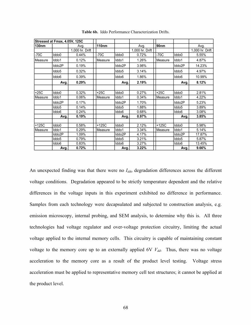
68
Table 6b. Iddo Performance Characterization Drifts.
Stressed at Fmax, 4.05V, 125C130nm Avg. 110nm Avg. 90nm Avg.
1,000 hr. Drift 1,000 hr. Drift 1,000 hr. Drift-70C Iddo0 0.44% -70C Iddo0 0.72% -70C Iddo0 5.55%Measure Iddo1 0.12% Measure Iddo1 1.26% Measure Iddo1 4.87%
Iddo2P 0.19% Iddo2P 3.98% Iddo2P 14.23%Iddo5 0.32% Iddo5 3.14% Iddo5 4.97%Iddo6 0.39% Iddo6 1.86% Iddo6 10.99%
Avg. 0.29% Avg. 2.19% Avg. 8.12%
+25C Iddo0 0.32% +25C Iddo0 0.27% +25C Iddo0 2.81%Measure Iddo1 0.06% Measure Iddo1 0.34% Measure Iddo1 4.22%
Iddo2P 0.17% Iddo2P 1.70% Iddo2P 5.23%Iddo5 0.14% Iddo5 1.88% Iddo5 3.89%Iddo6 0.24% Iddo6 0.68% Iddo6 3.08%
Avg. 0.19% Avg. 0.97% Avg. 3.85%
+125C Iddo0 0.58% +125C Iddo0 2.12% +125C Iddo0 5.98%Measure Iddo1 0.29% Measure Iddo1 3.34% Measure Iddo1 5.14%
Iddo2P 1.09% Iddo2P 4.17% Iddo2P 17.87%Iddo5 0.79% Iddo5 3.21% Iddo5 5.87%Iddo6 0.83% Iddo6 3.27% Iddo6 13.45%
Avg. 0.72% Avg. 3.22% Avg. 9.66%
An unexpected finding was that there were no Iddo degradation differences across the different
voltage conditions. Degradation appeared to be strictly temperature dependent and the relative
differences in the voltage inputs in this experiment exhibited no difference in performance.
Samples from each technology were decapsulated and subjected to construction analysis, e.g.
emission microscopy, internal probing, and SEM analysis, to determine why this is. All three
technologies had voltage regulator and over-voltage protection circuitry, limiting the actual
voltage applied to the internal memory cells. This circuitry is capable of maintaining constant
voltage to the memory core up to an externally applied 6V Vdd. Thus, there was no voltage
acceleration to the memory core as a result of the product level testing. Voltage stress
acceleration must be applied to representative memory cell test structures; it cannot be applied at
the product level.
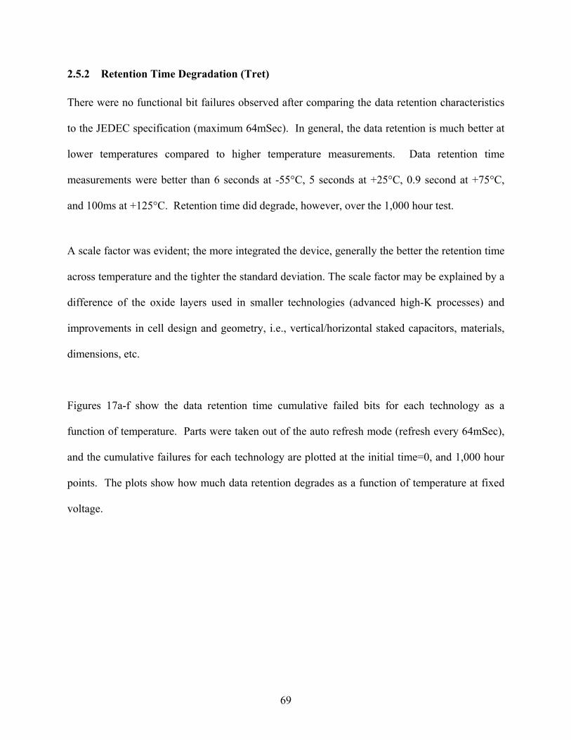
69
2.5.2 Retention Time Degradation (Tret)
There were no functional bit failures observed after comparing the data retention characteristics
to the JEDEC specification (maximum 64mSec). In general, the data retention is much better at
lower temperatures compared to higher temperature measurements. Data retention time
measurements were better than 6 seconds at -55°C, 5 seconds at +25°C, 0.9 second at +75°C,
and 100ms at +125°C. Retention time did degrade, however, over the 1,000 hour test.
A scale factor was evident; the more integrated the device, generally the better the retention time
across temperature and the tighter the standard deviation. The scale factor may be explained by a
difference of the oxide layers used in smaller technologies (advanced high-K processes) and
improvements in cell design and geometry, i.e., vertical/horizontal staked capacitors, materials,
dimensions, etc.
Figures 17a-f show the data retention time cumulative failed bits for each technology as a
function of temperature. Parts were taken out of the auto refresh mode (refresh every 64mSec),
and the cumulative failures for each technology are plotted at the initial time=0, and 1,000 hour
points. The plots show how much data retention degrades as a function of temperature at fixed
voltage.
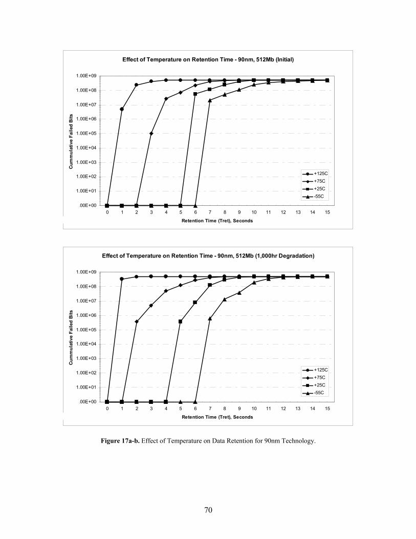
70
Figure 17a-b. Effect of Temperature on Data Retention for 90nm Technology.
Effect of Temperature on Retention Time - 90nm, 512Mb (Initial)
1.00E+00
1.00E+01
1.00E+02
1.00E+03
1.00E+04
1.00E+05
1.00E+06
1.00E+07
1.00E+08
1.00E+09
0 1 2 3 4 5 6 7 8 9 10 11 12 13 14 15
Retention Time (Tret), Seconds
Cum
mul
ativ
e Fa
iled
Bits
+125C+75C+25C-55C
Effect of Temperature on Retention Time - 90nm, 512Mb (1,000hr Degradation)
1.00E+00
1.00E+01
1.00E+02
1.00E+03
1.00E+04
1.00E+05
1.00E+06
1.00E+07
1.00E+08
1.00E+09
0 1 2 3 4 5 6 7 8 9 10 11 12 13 14 15
Retention Time (Tret), Seconds
Cum
mul
ativ
e Fa
iled
Bits
+125C+75C+25C-55C
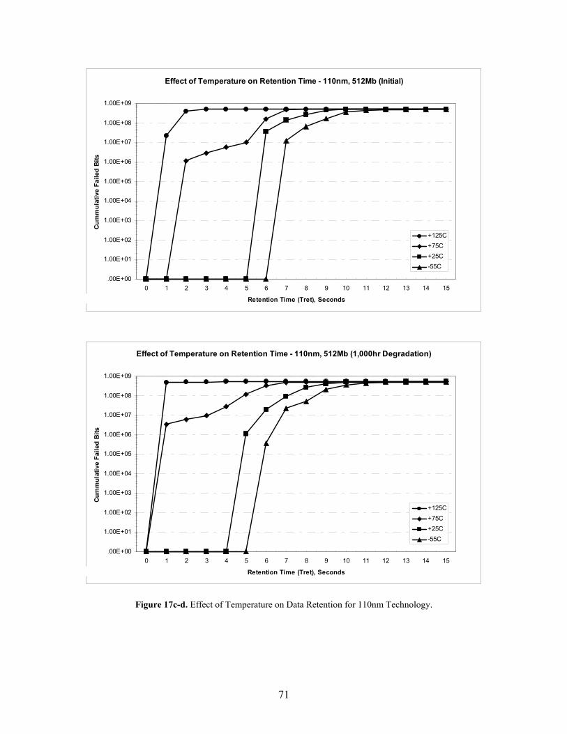
71
Figure 17c-d. Effect of Temperature on Data Retention for 110nm Technology.
Effect of Temperature on Retention Time - 110nm, 512Mb (Initial)
1.00E+00
1.00E+01
1.00E+02
1.00E+03
1.00E+04
1.00E+05
1.00E+06
1.00E+07
1.00E+08
1.00E+09
0 1 2 3 4 5 6 7 8 9 10 11 12 13 14 15
Retention Time (Tret), Seconds
Cum
mul
ativ
e Fa
iled
Bits
+125C+75C+25C-55C
Effect of Temperature on Retention Time - 110nm, 512Mb (1,000hr Degradation)
1.00E+00
1.00E+01
1.00E+02
1.00E+03
1.00E+04
1.00E+05
1.00E+06
1.00E+07
1.00E+08
1.00E+09
0 1 2 3 4 5 6 7 8 9 10 11 12 13 14 15
Retention Time (Tret), Seconds
Cum
mul
ativ
e Fa
iled
Bits
+125C+75C+25C-55C
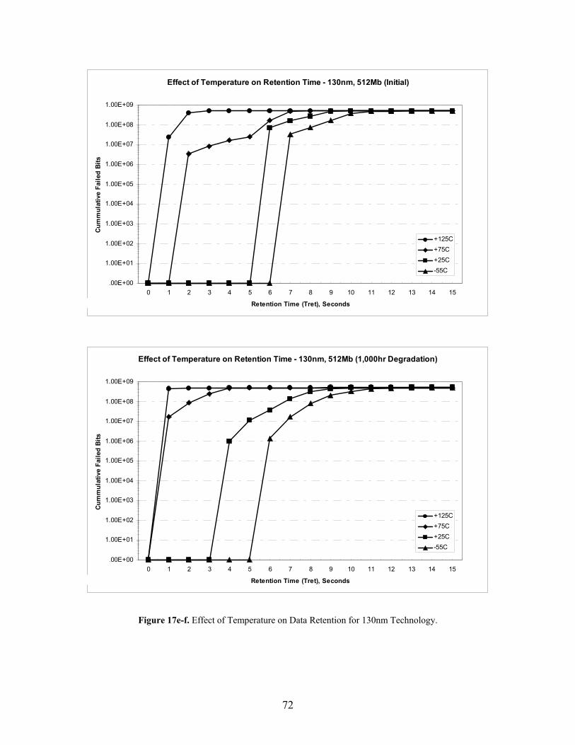
72
Figure 17e-f. Effect of Temperature on Data Retention for 130nm Technology.
Effect of Temperature on Retention Time - 130nm, 512Mb (Initial)
1.00E+00
1.00E+01
1.00E+02
1.00E+03
1.00E+04
1.00E+05
1.00E+06
1.00E+07
1.00E+08
1.00E+09
0 1 2 3 4 5 6 7 8 9 10 11 12 13 14 15
Retention Time (Tret), Seconds
Cum
mul
ativ
e Fa
iled
Bits
+125C+75C+25C-55C
Effect of Temperature on Retention Time - 130nm, 512Mb (1,000hr Degradation)
1.00E+00
1.00E+01
1.00E+02
1.00E+03
1.00E+04
1.00E+05
1.00E+06
1.00E+07
1.00E+08
1.00E+09
0 1 2 3 4 5 6 7 8 9 10 11 12 13 14 15
Retention Time (Tret), Seconds
Cum
mul
ativ
e Fa
iled
Bits
+125C+75C+25C-55C
73
Chapter 3: SDRAM Degradation and Predictive Model
3.1 Acceleration Model
Physical acceleration models based upon the physical or chemical theory that describes the
failure causing process over the range of data may be employed for well understood failure
mechanisms. Usually, individual test structures are utilized in the DOE to more accurately
measure threshold voltage (Vt), drain current (Idsat), and transconductance (gm) shifts, as well as
dielectric breakdown over a range of stress conditions. At the complex product level, such as the
512Mb SDRAM, it is difficult to identify the exact physical mechanism causing minute physical
characteristic changes embedded deep within the internal circuitry from product level data.
Often we are constrained by the product performance degradation to develop empirical-based
acceleration models that fit the observed data.
Data retention (Tret) characteristics were determined to be the best measurable indicator of the
performance degradation of the DRAMs, as the storage cell’s critical function is to retain a
charge representing its state. Each DRAM was tested until each memory cell lost its ability to
store a ‘1’ in the memory bit locale. Since all bits were run to failure, the data is said to be
complete with no right-censoring. Due to the high number of repetitive bits of information in
each memory product, a significant sample size was examined from a limited number of
products. Data retention tests at 100 hour increments, up to 1,000 hours, revealed how the
retention time degrades over time. The performance data was analyzed by fitting a degradation
model to the data showing the relationship between performance, age, stress and technology.
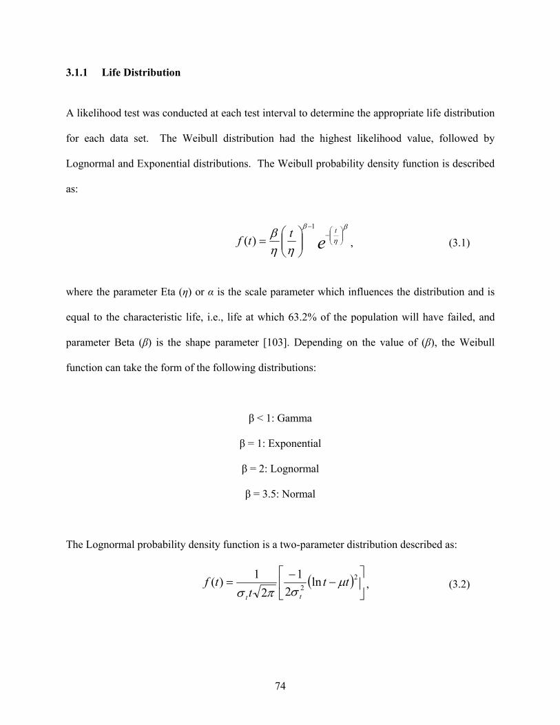
74
3.1.1 Life Distribution
A likelihood test was conducted at each test interval to determine the appropriate life distribution
for each data set. The Weibull distribution had the highest likelihood value, followed by
Lognormal and Exponential distributions. The Weibull probability density function is described
as:
β
η
β
ηηβ e
tttf ⎟⎟⎠
⎞⎜⎜⎝
⎛−
−
⎟⎟⎠
⎞⎜⎜⎝
⎛=
1
)( , (3.1)
where the parameter Eta (η) or α is the scale parameter which influences the distribution and is
equal to the characteristic life, i.e., life at which 63.2% of the population will have failed, and
parameter Beta (β) is the shape parameter [103]. Depending on the value of (β), the Weibull
function can take the form of the following distributions:
β < 1: Gamma
β = 1: Exponential
β = 2: Lognormal
β = 3.5: Normal
The Lognormal probability density function is a two-parameter distribution described as:
( ) ⎥⎦
⎤⎢⎣
⎡−
−= 2
2 ln2
12
1)( ttt
tftt
μσπσ
, (3.2)
75
where µ = E (ln t) and 2tσ = var (ln t). The failure rate initially increases with time and then
decreases depending on the values of parameters µ and σt [103].
The Exponential probability density function is described as:
( )e ttf λλ −=)( , (3.3)
where the parameter Lambda (λ) is the rate of occurrence in time interval (t).
3.1.2 Multivariable Life-Stress Relationship
In the case where there is more than one accelerating variable, both should be considered in the
life-stress relationship. Temperature and voltage are the two stress factors in this experiment,
therefore, the Arrhenius and the Inverse Power Law models may be combined to yield the
Temperature – Non-Thermal (T-NT) Model [104]:
e VB
nU
CVUL−
=),( , (3.4)
where,
• L represents a quantifiable life measure, such as mean life, characteristic life, median life
or B(x) life, etc.
• U is the non-thermal stress (voltage),
• V is the temperature in absolute units,
• B is one of the model parameters to be determined derived from the relationship:
76
15623.8 −−==eVKeenergyactivation
KEaB
• C and n are the 2nd and 3rd model parameters to be determined, (C > 0).
This relationship can be linearized by taking the LN of both sides:
( ) ( ) ( )VBUnCVUL +−= lnln),(ln . (3.5)
The acceleration factor for the T-NT relationship is explained by:
, (3.6)
where,
• Luse is one life at use stress level,
• LAccelerated is the life at the accelerated stress level,
• Vu is the use temperature,
• VA is the accelerated temperature,
• UA is the accelerated voltage,
• Uu is the use voltage,
• B is one of the model parameters to be determined derived from the relationship:
77
15623.8 −−==eVKeenergyactivation
KEaB
• C and n are the 2nd and 3rd model parameters to be determined, (C > 0).
Combining the joint distribution of stress and life, the Weibull life pdf becomes:
(3.7)
by setting η or α = L(U,V) from Equation (4.4).
Expanding upon the statistical properties of the T-NT Weibull Model, the Mean or MTTF is:
⎟⎟⎠
⎞⎜⎜⎝
⎛+Γ=
−11*
βe VB
nU
CT , (3.8)
where ⎟⎟⎠
⎞⎜⎜⎝
⎛+Γ 11
β is the Gamma function evaluated at the value of ⎟⎟
⎠
⎞⎜⎜⎝
⎛+11
β.
The standard deviation, σT, is given by:
2
1112* ⎟⎟⎠
⎞⎜⎜⎝
⎛⎟⎟⎠
⎞⎜⎜⎝
⎛+Γ−⎟⎟
⎠
⎞⎜⎜⎝
⎛+Γ=
− ββσ
e VB
nT
U
C. (3.9)
78
The Reliability function of the T-NT Weibull Model is described as:
β
⎟⎟⎟⎟⎟⎟
⎠
⎞
⎜⎜⎜⎜⎜⎜
⎝
⎛
−
−
= C
VB
enTUVUTR e),,( , (3.10)
and the Conditional Reliability function as specified stress level, t, is given by:
( )( )
( )
β
β
⎟⎟⎟⎟⎟⎟
⎠
⎞
⎜⎜⎜⎜⎜⎜
⎝
⎛
−
⎟⎟⎟⎟⎟⎟⎟
⎠
⎞
⎜⎜⎜⎜⎜⎜⎜
⎝
⎛
−
−
−
+
=+
=
C
C
VB
VB
enTU
enUtT
VUTRVUtTRVUtTR
e
e,,
),,),,,( . (3.11)
The T-NT Weibull failure rate function, λ(T), is described as:
( )( )
1
*,,
),,),,(
−−−
⎟⎟⎟⎟
⎠
⎞
⎜⎜⎜⎜
⎝
⎛
==
β
βλ
C
n
CVUTRVUTfVUT
VB
VB
eTUUe, (3.12)
and Reliable Life, TR, of a unit for a specified reliability starting at age zero is given by:
79
( )[ ] β1
,,ln* VUTRU
CT R
VB
nR
e−=
−. (3.13)
The Maximum Likelihood Estimation for parameter determination is given by substituting the T-
NT Model into the Weibull Log-Likelihood function, yielding:
, (3.14)
where,
• F is the number of groups of exact times-to-failure data points,
• Ni is the number of times-to-failure data points in the ith time-to-failure data group,
• β is the Weibull shape parameter (unknown, the 1st of four parameters to be estimated),
• B is the first T-NT parameter (unknown, the 2nd of four parameters to be estimated),
• C is the second T-NT parameter (unknown, the 3rd of four parameters to be estimated),
• n is the third T-NT parameter (unknown, the 4th of four parameters to be estimated),
• Vi is the temperature stress level of the ith group,
• Ui is the voltage stress level of the ith group,

80
• Ti is the exact failure time of the ith group,
• S is the number of groups of suspension data points,
• N’i is the number of suspensions in the ith group of suspension data points, and
• T’i is the running time of the ith suspension data group.
The parameter estimate solutions are found by solving for the parameters B, C, n and β so that:
0,0,0,0 =∂Λ∂
=∂Λ∂
=∂Λ∂
=∂Λ∂
βand
nCB .
Finally, the Maximum Likelihood Estimation for standard deviation parameter determination is
given by:
, (3.15)
where,
• F is the number of groups of exact times-to-failure data points,
• Ni is the number of times-to-failure data points in the ith time-to-failure data group,
• σT is the standard deviation of the natural logarithm of the time-to-failure (unknown, the
1st of four parameters to be estimated),
• B is the first T-NT parameter (unknown, the 2nd of four parameters to be estimated),
81
• C is the second T-NT parameter (unknown, the 3rd of four parameters to be estimated),
• n is the third T-NT parameter (unknown, the 4th of four parameters to be estimated),
• Vi is the temperature stress level of the ith group,
• Ui is the voltage stress level of the ith group,
• Ti is the exact failure time of the ith group,
• S is the number of groups of suspension data points,
• N’i is the number of suspensions in the ith group of suspension data points, and
• T’i is the running time of the ith suspension data group.
and,
( )2
)(21
*21 e xx −=π
φ ,
(3.16)
( ) dtxx t
e∫∞−
−=Φ 2
2
*21π
.
The parameter estimate solutions are found by solving for the parameters 'ˆTσ , B , C , n so that:
0ˆ
,0ˆ,0ˆ,0ˆ '
=∂Λ∂
=∂Λ∂
=∂Λ∂
=∂Λ∂
nand
CBTσ.
3.2 Data Analysis
Data from the accelerated test of each of the three technologies were analyzed and plotted using
Reliasoft’s Alta 6.5 and Weibull ++7. First, combining the joint distribution of life with
temperature and voltage stresses, the Weibull life pdf (Eq. 4.7) was used to model the behavior
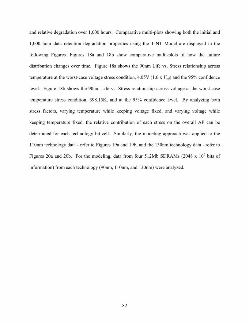
82
and relative degradation over 1,000 hours. Comparative multi-plots showing both the initial and
1,000 hour data retention degradation properties using the T-NT Model are displayed in the
following Figures. Figures 18a and 18b show comparative multi-plots of how the failure
distribution changes over time. Figure 18a shows the 90nm Life vs. Stress relationship across
temperature at the worst-case voltage stress condition, 4.05V (1.6 x Vdd) and the 95% confidence
level. Figure 18b shows the 90nm Life vs. Stress relationship across voltage at the worst-case
temperature stress condition, 398.15K, and at the 95% confidence level. By analyzing both
stress factors, varying temperature while keeping voltage fixed, and varying voltage while
keeping temperature fixed, the relative contribution of each stress on the overall AF can be
determined for each technology bit-cell. Similarly, the modeling approach was applied to the
110nm technology data - refer to Figures 19a and 19b, and the 130nm technology data - refer to
Figures 20a and 20b. For the modeling, data from four 512Mb SDRAMs (2048 x 106 bits of
information) from each technology (90nm, 110nm, and 130nm) were analyzed.
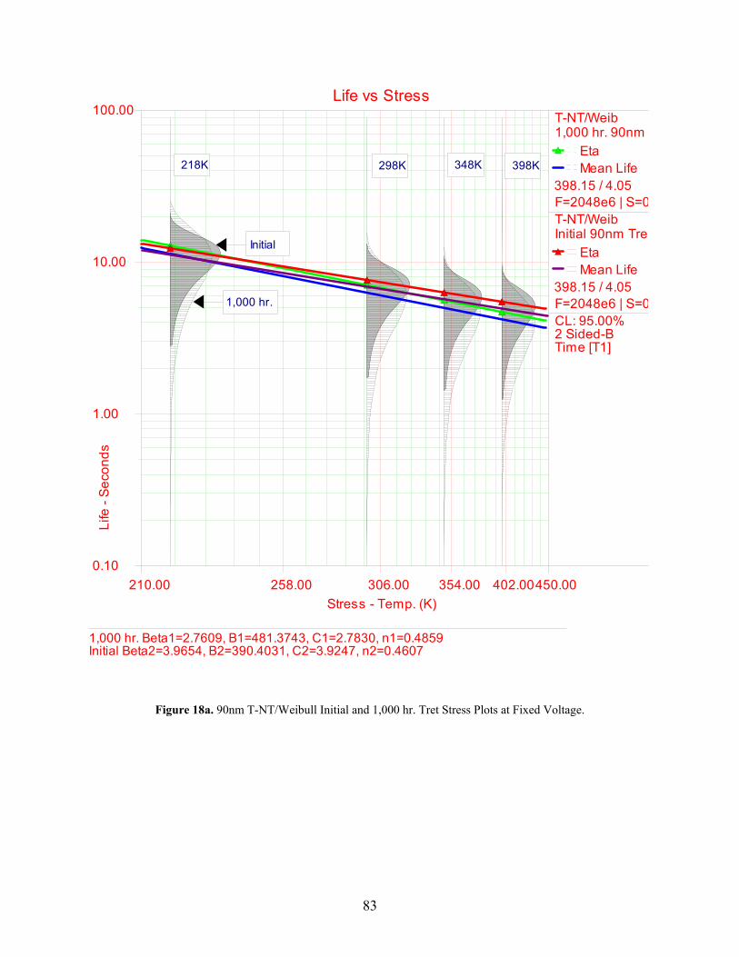
83
Figure 18a. 90nm T-NT/Weibull Initial and 1,000 hr. Tret Stress Plots at Fixed Voltage.
0.10
100.00
1.00
10.00
450.00210.00 258.00 306.00 354.00 402.00
Life vs Stress
Stress - Temp. (K)
Life
- Se
cond
sT-NT/Weib1,000 hr. 90nm
EtaMean Life
398.15 / 4.05F=2048e6 | S=0T-NT/WeibInitial 90nm Tret
EtaMean Life
398.15 / 4.05F=2048e6 | S=0CL: 95.00%2 Sided-BTime [T1]
218K 298K 348K 398K
Initial
1,000 hr.
1,000 hr. Beta1=2.7609, B1=481.3743, C1=2.7830, n1=0.4859Initial Beta2=3.9654, B2=390.4031, C2=3.9247, n2=0.4607
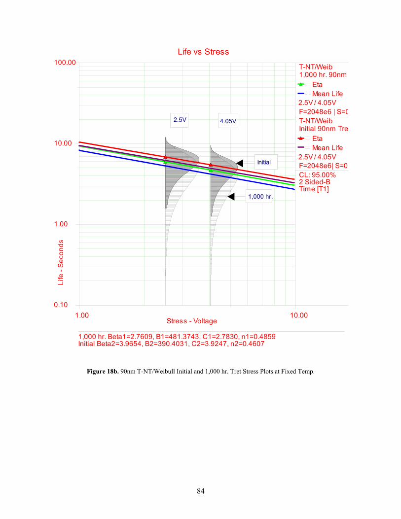
84
Figure 18b. 90nm T-NT/Weibull Initial and 1,000 hr. Tret Stress Plots at Fixed Temp.
1.00 10.000.10
100.00
1.00
10.00
Life vs Stress
Stress - Voltage
Life
- Se
cond
sT-NT/Weib1,000 hr. 90nm
EtaMean Life
2.5V / 4.05VF=2048e6 | S=0T-NT/WeibInitial 90nm Tret
EtaMean Life
F=2048e6| S=0CL: 95.00%2 Sided-BTime [T1]
1,000 hr. Beta1=2.7609, B1=481.3743, C1=2.7830, n1=0.4859Initial Beta2=3.9654, B2=390.4031, C2=3.9247, n2=0.4607
2.5V / 4.05VInitial
1,000 hr.
2.5V 4.05V

85
Figure 19a. 110nm T-NT/Weibull Initial and 1,000 hr. Tret Stress Plots at Fixed Voltage.
0.10
100.00
1.00
10.00
450.00210.00 258.00 306.00 354.00 402.00
Life vs Stress
Stress - Temp. (K)
Life
- Se
cond
sT-NT/Weib1,000 hr. 110nm T
EtaMean Life
398.5 / 4.05F=2048e6 | S=0T-NT/WeibInitial 110nm Tret
EtaMean Life
398.5 / 4.05F=2048e6 | S=0CL: 95.00%2 Sided-BTime [T1]
218K 298K 348K 398K
Initial
1,000 hr.
1,000 hr. Beta1=2.5998, B1=463.7186, C1=2.9125, n1=0.5048Initial Beta2=3.7014, B2=375.6892, C2=4.0526, n2=0.4736
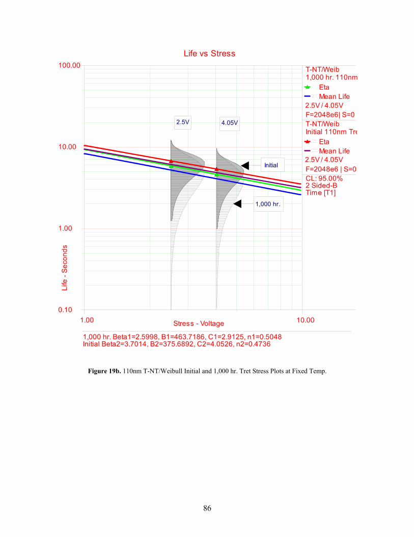
86
Figure 19b. 110nm T-NT/Weibull Initial and 1,000 hr. Tret Stress Plots at Fixed Temp.
1.00 10.000.10
100.00
1.00
10.00
Life vs Stress
Stress - Voltage
Life
- Se
cond
sT-NT/Weib1,000 hr. 110nm
EtaMean Life
2.5V / 4.05VF=2048e6| S=0T-NT/WeibInitial 110nm Tre
EtaMean Life
F=2048e6 | S=0CL: 95.00%2 Sided-BTime [T1]
1,000 hr. Beta1=2.5998, B1=463.7186, C1=2.9125, n1=0.5048Initial Beta2=3.7014, B2=375.6892, C2=4.0526, n2=0.4736
2.5V / 4.05V
2.5V 4.05V
Initial
1,000 hr.
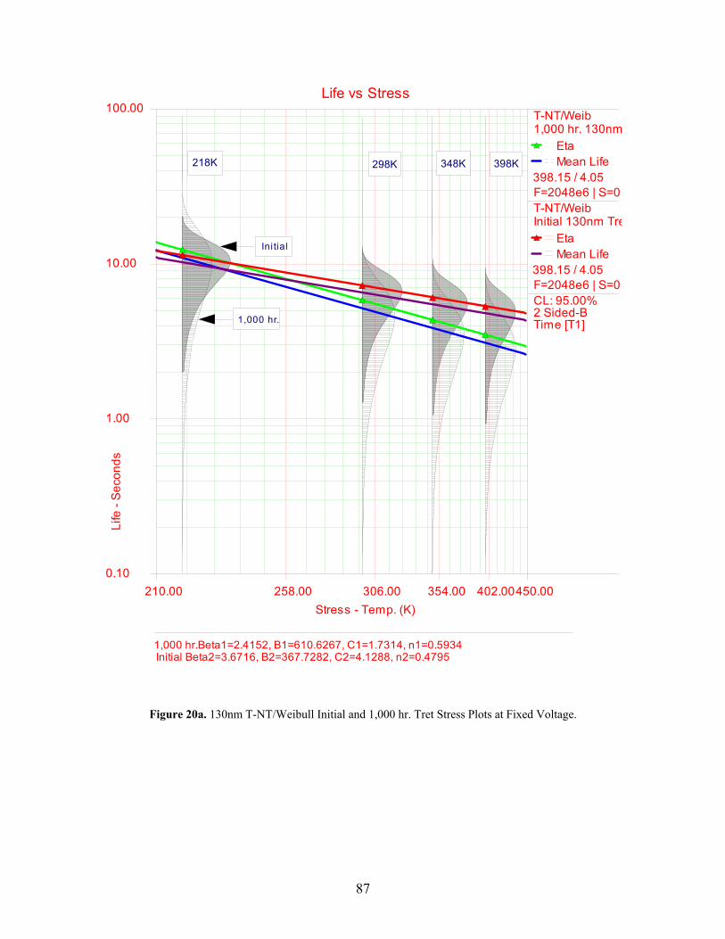
87
Figure 20a. 130nm T-NT/Weibull Initial and 1,000 hr. Tret Stress Plots at Fixed Voltage.
0.10
100.00
1.00
10.00
450.00210.00 258.00 306.00 354.00 402.00
Life vs Stress
Stress - Temp. (K)
Life
- Se
cond
sT-NT/Weib1,000 hr. 130nm
EtaMean Life
398.15 / 4.05F=2048e6 | S=0T-NT/WeibInitial 130nm Tre
EtaMean Life
398.15 / 4.05F=2048e6 | S=0CL: 95.00%2 Sided-BTime [T1]
Initial
1,000 hr.
348K 398K218K 298K
1,000 hr.Beta1=2.4152, B1=610.6267, C1=1.7314, n1=0.5934Initial Beta2=3.6716, B2=367.7282, C2=4.1288, n2=0.4795
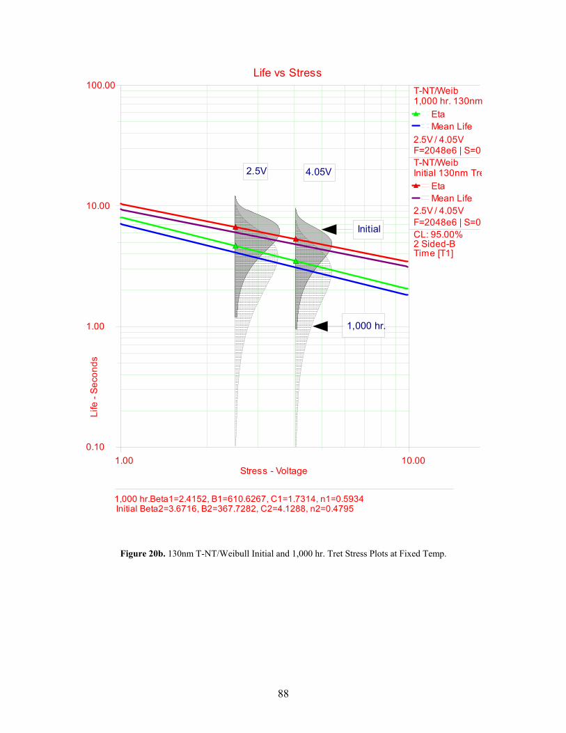
88
Figure 20b. 130nm T-NT/Weibull Initial and 1,000 hr. Tret Stress Plots at Fixed Temp.
1.00 10.000.10
100.00
1.00
10.00
Life vs Stress
Stress - Voltage
Life
- Se
cond
sT-NT/Weib1,000 hr. 130nm
EtaMean Life
2.5V / 4.05VF=2048e6 | S=0T-NT/WeibInitial 130nm Tre
EtaMean Life
F=2048e6 | S=0CL: 95.00%2 Sided-BTime [T1]
2.5V / 4.05V
2.5V 4.05V
Initial
1,000 hr.
1,000 hr.Beta1=2.4152, B1=610.6267, C1=1.7314, n1=0.5934Initial Beta2=3.6716, B2=367.7282, C2=4.1288, n2=0.4795
89
Model parameters for the T-NT Weibull Model were calculated for each technology up to the
end of the time terminated stress test, 1,000 hour point. Model parameters and statistics for each
technology and stress condition are summarized in Tables 7 and 8. The retention time Mean (Eq.
3.8) and Std. Deviation (Eq. 3.9) were calculated for each technology at both stress voltages and
at four temperatures. Other temperature and voltage stress combinations may also be calculated
for the desired use condition.
A Use-Level Weibull Probability plot showing the changing Beta slope of the 90nm technology
parts at worst-case test conditions, 398.15K and 4.05V, is shown in Figure 21. Likewise,
equivalent plots may be created for any of the combinations of stress temperatures and voltages.
The plot shows a decreasing Beta slope over time. The Beta slopes of the 110nm and 130nm
technology parts exhibit similar characteristics. Figure 21 shows a decreasing β over time,
3.9654 initially vs. 2.7609 at the 1,000 hr. point. All three regions of the bath-tub curve are
represented by the Weibull distribution as determined by the value of the shape-parameter, β.
The Weibull distribution is appropriate for complex components or systems composed of a
number of constituent components whose failure is governed by the most severe defect or
weakest link. For 0 < β < 1, the distribution indicates an early or infant mortality behavior with a
decreasing failure rate. For β = 1, the distribution reduces to the exponential distribution
reflecting CFR region of the bath-tub curve. For β > 1, the distribution reflects an increasing
failure rate and models the wearout region of the bath-tub curve [105].
90
Figure 22 shows the changing reliability vs. time of the data retention time degradation after
1,000 hours at worst-case test conditions, 398.15K and 4.05V. The Reliability vs. Time plots
using Eq. 3.10 for the 110nm and 130nm technology parts reveal a comparable shift over time.
The impact of stress on data retention failure rate over time is shown in Figure 23 for the 90nm
technology parts. Eq. 3.12 was used for this calculation. The impact on FR over time from the
changing Beta is evident in this figure. Comparable shifts were revealed for the 110nm and
130nm technology parts.
Figure 24 shows the Standard Deviation Plot for the 90nm technology parts across temperature at
worst-case voltage conditions, 4.05V, at initial and 1,000 hr. points. Using Eq. 3.9, one can see
in Figure 24 the increase in standard deviation over time. Comparable shifts were observed for
the 110nm and 130nm technology parts.
91
Table 7. Thermal – Non-Thermal Weibull Model Distribution Paramaters (4.05V).
Thermal - Non-Thermal/Weibull Model Distributions90nm-Initial Parameters 110nm-Initial Parameters 130nm-Initial Parameters
Parameter Bounds Parameter Bounds Parameter BoundsLower = 3.9624 Beta = 3.9654 Upper = 3.9685 Lower = 3.6984 Beta = 3.7014 Upper = 3.7044 Lower = 3.6687 Beta = 3.6716 Upper = 3.6746Lower = 389.9964 B = 390.4031 Upper = 390.8098 Lower = 375.2421 B = 375.6892 Upper = 376.1363 Lower = 367.2766 B = 367.7282 Upper = 368.1797Lower = 3.9179 C = 3.9247 Upper = 3.9315 Lower = 4.0449 C = 4.0526 Upper = 4.0603 Lower = 4.1209 C = 4.1288 Upper = 4.1367Lower = 0.4597 n = 0.4607 Upper = 0.4617 Lower = 0.4725 n = 0.4736 Upper = 0.4747 Lower = 0.4784 n = 0.4795 Upper = 0.4806Eta = 5.4930 Eta = 5.3639 Eta = 5.3168Ea = 0.0336 Ea = 0.0324 Ea = 0.0317Temperature (K) = 398.15 Temperature (K) = 398.15 Temperature (K) = 398.15Voltage (V) = 4.05 Voltage (V) = 4.05 Voltage (V) = 4.05Confidence Bounds = 2-Sided @ 95% CL Std Dev Confidence Bounds = 2-Sided @ 95% CL Std Dev Confidence Bounds = 2-Sided @ 95% CL Std DevUpper Limit = 4.979 Upper Limit = 4.8436 Upper Limit = 4.7989Mean Life (Secs.) = 4.9764 1.42 Mean Life (Secs.) = 4.8408 1.46 Mean Life (Secs.) = 4.7961 1.49Lower Limit = 4.9737 Lower Limit = 4.8379 Lower Limit = 4.7933Temperature (K) = 348.15 Temperature (K) = 348.15 Temperature (K) = 348.15Voltage (V) = 4.05 Voltage (V) = 4.05 Voltage (V) = 4.05Confidence Bounds = 2-Sided @ 95% CL Confidence Bounds = 2-Sided @ 95% CL Confidence Bounds = 2-Sided @ 95% CLUpper Limit = 5.7315 Upper Limit = 5.5445 Upper Limit = 5.4791Mean Life (Secs.) = 5.7289 1.63 Mean Life = 5.5419 1.65 Mean Life (Secs.) = 5.4764 1.67Lower Limit = 5.7263 Lower Limit = 5.5392 Lower Limit = 5.4738Temperature (K) = 298.15 Temperature (K) = 298.15 Temperature (K) = 298.15Voltage (V) = 4.05 Voltage (V) = 4.05 Voltage (V) = 4.05Confidence Bounds = 2-Sided @ 95% CL Confidence Bounds = 2-Sided @ 95% CL Confidence Bounds = 2-Sided @ 95% CLUpper Limit = 6.9169 Upper Limit = 6.6413 Upper Limit = 6.5404Mean Life (Secs.) = 6.9142 1.95 Mean Life = 6.6386 2.01 Mean Life (Secs.) = 6.5377 1.98Lower Limit = 6.9115 Lower Limit = 6.6359 Lower Limit = 6.535Temperature (K) = 218.15 Temperature (K) = 218.15 Temperature (K) = 218.15Voltage (V) = 4.05 Voltage (V) = 4.05 Voltage (V) = 4.05Confidence Bounds = 2-Sided @ 95% CL Confidence Bounds = 2-Sided @ 95% CL Confidence Bounds = 2-Sided @ 95% CLUpper Limit = 11.1827 Upper Limit = 10.5315 Upper Limit = 10.2836Mean Life (Secs.) = 11.176 3.24 Mean Life = 10.5246 3.27 Mean Life (Secs.) = 10.2767 3.15Lower Limit = 11.1692 Lower Limit = 10.5177 Lower Limit = 10.2699
Fisher Var/Cov Matrix Fisher Var/Cov Matrix Fisher Var/Cov Matrix
VarBeta CovBetaB CovBetaC CovBetan VarBeta CovBetaB CovBetaC CovBetan VarBeta CovBetaB CovBetaC CovBetan2.45E-06 -4.03E-05 5.40E-07 -5.22E-08 2.33E-06 -4.79E-05 6.82E-07 -4.76E-08 2.31E-06 -5.28E-05 7.58E-07 -4.90E-08
CovBetaB VarB CovBC CovBn CovBetaB VarB CovBC CovBn CovBetaB VarB CovBC CovBn-4.03E-05 4.30E-02 -5.21E-04 1.02E-05 -4.79E-05 5.20E-02 -6.58E-04 1.05E-05 -5.28E-05 5.30E-02 -6.85E-04 1.05E-05
CovBetaC CovBC VarC CovCn CovBetaC CovBC VarC CovCn CovBetaC CovBC VarC CovCn5.40E-07 -5.21E-04 1.20E-05 1.09E-06 6.82E-07 -6.58E-04 1.54E-05 1.30E-06 7.58E-07 -6.85E-04 1.63E-05 1.35E-06
CovBetan CovBn CovCn Varn CovBetan CovBn CovCn Varn CovBetan CovBn CovCn Varn-5.22E-08 1.02E-05 1.09E-06 2.70E-07 -4.76E-08 1.05E-05 1.30E-06 3.09E-07 -4.90E-08 1.05E-05 1.35E-06 3.14E-07
Thermal - Non-Thermal/Weibull Model Distributions90nm-Final Parameters 110nm-Final Parameters 130nm-Final Parameters
Parameter Bounds Parameter Bounds Parameter BoundsLower = 2.7586 Beta = 2.7609 Upper = 2.7632 Lower = 2.5976 Beta = 2.5998 Upper = 2.6019 Lower = 2.4134 Beta = 2.4152 Upper = 2.4171Lower = 480.7776 B = 481.3743 Upper = 481.9710 Lower = 463.0570 B = 463.7186 Upper = 464.3802 Lower = 609.9189 B = 610.6267 Upper = 611.3345Lower = 2.7759 C = 2.7830 Upper = 2.7901 Lower = 2.9045 C = 2.9125 Upper = 2.9206 Lower = 1.7264 C = 1.7314 Upper = 1.7364Lower = 0.4844 n = 0.4859 Upper = 0.4873 Lower = 0.5032 n = 0.5048 Upper = 0.5063 Lower = 0.5917 n = 0.5934 Upper = 0.5951Eta = 4.7255 Eta = 4.6027 Eta = 3.4993Ea = 0.0415 Ea = 0.0400 Ea = 0.0526Temperature (K) = 398.15 Temperature (K) = 398.15 Temperature (K) = 398.15Voltage (V) = 4.05 Voltage (V) = 4.05 Voltage (V) = 4.05Confidence Bounds = 2-Sided @ 95% CL Std Dev Confidence Bounds = 2-Sided @ 95% CL Std Dev Confidence Bounds = 2-Sided @ 95% CL Std DevUpper Limit = 4.2089 Upper Limit = 4.0915 Upper Limit = 3.1053Mean Life (Secs.) = 4.2056 1.59 Mean Life (Secs.) = 4.0881 1.63 Mean Life (Secs.) = 3.1024 1.42Lower Limit = 4.2024 Lower Limit = 4.0847 Lower Limit = 3.0996Temperature (K) = 348.15 Temperature (K) = 348.15 Temperature (K) = 348.15Voltage (V) = 4.05 Voltage (V) = 4.05 Voltage (V) = 4.05Confidence Bounds = 2-Sided @ 95% CL Confidence Bounds = 2-Sided @ 95% CL Confidence Bounds = 2-Sided @ 95% CLUpper Limit = 5.0063 Upper Limit = 4.8342 Upper Limit = 3.8698Mean Life (Secs.) = 5.0031 2.01 Mean Life (Secs.) = 4.8309 1.99 Mean Life (Secs.) = 3.8669 1.72Lower Limit = 4.9999 Lower Limit = 4.8276 Lower Limit = 3.864Temperature (K) = 298.15 Temperature (K) = 298.15 Temperature (K) = 298.15Voltage (V) = 4.05 Voltage (V) = 4.05 Voltage (V) = 4.05Confidence Bounds = 2-Sided @ 95% CL Confidence Bounds = 2-Sided @ 95% CL Confidence Bounds = 2-Sided @ 95% CLUpper Limit = 6.3122 Upper Limit = 6.0406 Upper Limit = 5.1925Mean Life (Secs.) = 6.3087 2.49 Mean Life (Secs.) = 6.0371 2.52 Mean Life (Secs.) = 5.1892 2.35Lower Limit = 6.3053 Lower Limit = 6.0336 Lower Limit = 5.1859Temperature (K) = 218.15 Temperature (K) = 218.15 Temperature (K) = 218.15Voltage (V) = 4.05 Voltage (V) = 4.05 Voltage (V) = 4.05Confidence Bounds = 2-Sided @ 95% CL Confidence Bounds = 2-Sided @ 95% CL Confidence Bounds = 2-Sided @ 95% CLUpper Limit = 11.4145 Upper Limit = 10.6723 Upper Limit = 11.0083Mean Life (Secs.) = 11.4046 4.39 Mean Life (Secs.) = 10.6622 4.42 Mean Life (Secs.) = 10.9972 4.82Lower Limit = 11.3947 Lower Limit = 10.6521 Lower Limit = 10.986
Fisher Var/Cov Matrix Fisher Var/Cov Matrix Fisher Var/Cov Matrix
VarBeta CovBetaB CovBetaC CovBetan VarBeta CovBetaB CovBetaC CovBetan VarBeta CovBetaB CovBetaC CovBetan1.35E-06 -7.06E-05 6.73E-07 -4.90E-08 1.23E-06 -6.76E-05 6.41E-07 -5.92E-08 8.90E-07 -5.14E-05 2.24E-07 -9.17E-08
CovBetaB VarB CovBC CovBn CovBetaB VarB CovBC CovBn CovBetaB VarB CovBC CovBn-7.06E-05 9.27E-02 -8.10E-04 1.80E-05 -6.76E-05 1.14E-01 -1.04E-03 2.16E-05 -5.14E-05 1.30E-01 -6.75E-04 4.13E-05
CovBetaC CovBC VarC CovCn CovBetaC CovBC VarC CovCn CovBetaC CovBC VarC CovCn6.73E-07 -8.10E-04 1.30E-05 1.61E-06 6.41E-07 -1.04E-03 1.69E-05 1.89E-06 2.24E-07 -6.75E-04 6.52E-06 1.23E-06
CovBetan CovBn CovCn Varn CovBetan CovBn CovCn Varn CovBetan CovBn CovCn Varn-4.90E-08 1.80E-05 1.61E-06 5.55E-07 -5.92E-08 2.16E-05 1.89E-06 6.27E-07 -9.17E-08 4.13E-05 1.23E-06 7.39E-07
92
Table 8. Thermal – Non-Thermal Weibull Model Distribution Paramaters (2.5V).
Thermal - Non-Thermal/Weibull Model Distributions90nm-Initial Parameters 110nm-Initial Parameters 130nm-Initial Parameters
Parameter Bounds Parameter Bounds Parameter BoundsLower = 3.9624 Beta = 3.9654 Upper = 3.9685 Lower = 3.6984 Beta = 3.7014 Upper = 3.7044 Lower = 3.6687 Beta = 3.6716 Upper = 3.6746Lower = 389.9964 B = 390.4031 Upper = 390.8098 Lower = 375.2421 B = 375.6892 Upper = 376.1363 Lower = 367.2766 B = 367.7282 Upper = 368.1797Lower = 3.9179 C = 3.9247 Upper = 3.9315 Lower = 4.0449 C = 4.0526 Upper = 4.0603 Lower = 4.1209 C = 4.1288 Upper = 4.1367Lower = 0.4597 n = 0.4607 Upper = 0.4617 Lower = 0.4725 n = 0.4736 Upper = 0.4747 Lower = 0.4784 n = 0.4795 Upper = 0.4806Eta = 6.86 Eta = 6.7407 Eta = 6.7006Ea = 0.0336 Ea = 0.0324 Ea = 0.0317Temperature (K) = 398.15 Temperature (K) = 398.15 Temperature (K) = 398.15Voltage (V) = 2.5 Voltage (V) = 2.5 Voltage (V) = 2.5Confidence Bounds = 2-Sided @ 95% CL Std Dev Confidence Bounds = 2-Sided @ 95% CL Std Dev Confidence Bounds = 2-Sided @ 95% CL Std DevUpper Limit = 6.218 Upper Limit = 6.0866 Upper Limit = 6.0478Mean Life (Secs.) = 6.2149 1.75 Mean Life (Secs.) = 6.0833 1.81 Mean Life (Secs.) = 6.0444 1.81Lower Limit = 6.2118 Lower Limit = 6.08 Lower Limit = 6.0411Temperature (K) = 348.15 Temperature (K) = 348.15 Temperature (K) = 348.15Voltage (V) = 2.5 Voltage (V) = 2.5 Voltage (V) = 2.5Confidence Bounds = 2-Sided @ 95% CL Confidence Bounds = 2-Sided @ 95% CL Confidence Bounds = 2-Sided @ 95% CLUpper Limit = 7.1576 Upper Limit = 6.9675 Upper Limit = 6.9049Mean Life (Secs.) = 7.1547 2.06 Mean Life = 6.9644 2.23 Mean Life (Secs.) = 6.9018 2.18Lower Limit = 7.1517 Lower Limit = 6.9612 Lower Limit = 6.8987Temperature (K) = 298.15 Temperature (K) = 298.15 Temperature (K) = 298.15Voltage (V) = 2.5 Voltage (V) = 2.5 Voltage (V) = 2.5Confidence Bounds = 2-Sided @ 95% CL Confidence Bounds = 2-Sided @ 95% CL Confidence Bounds = 2-Sided @ 95% CLUpper Limit = 8.6382 Upper Limit = 8.346 Upper Limit = 8.2426Mean Life (Secs.) = 8.635 2.41 Mean Life = 8.3426 2.5 Mean Life (Secs.) = 8.2393 2.48Lower Limit = 8.6317 Lower Limit = 8.3393 Lower Limit = 8.236Temperature (K) = 218.15 Temperature (K) = 218.15 Temperature (K) = 218.15Voltage (V) = 2.5 Voltage (V) = 2.5 Voltage (V) = 2.5Confidence Bounds = 2-Sided @ 95% CL Confidence Bounds = 2-Sided @ 95% CL Confidence Bounds = 2-Sided @ 95% CLUpper Limit = 13.9663 Upper Limit = 13.2351 Upper Limit = 12.9605Mean Life (Secs.) = 13.9574 3.9 Mean Life = 13.2261 4.01 Mean Life (Secs.) = 12.9515 3.96Lower Limit = 13.9485 Lower Limit = 13.217 Lower Limit = 12.9426
Fisher Var/Cov Matrix Fisher Var/Cov Matrix Fisher Var/Cov Matrix
VarBeta CovBetaB CovBetaC CovBetan VarBeta CovBetaB CovBetaC CovBetan VarBeta CovBetaB CovBetaC CovBetan2.45E-06 -4.03E-05 5.40E-07 -5.22E-08 2.33E-06 -4.79E-05 6.82E-07 -4.76E-08 2.31E-06 -5.28E-05 7.58E-07 -4.90E-08
CovBetaB VarB CovBC CovBn CovBetaB VarB CovBC CovBn CovBetaB VarB CovBC CovBn-4.03E-05 4.30E-02 -5.21E-04 1.02E-05 -4.79E-05 5.20E-02 -6.58E-04 1.05E-05 -5.28E-05 5.30E-02 -6.85E-04 1.05E-05
CovBetaC CovBC VarC CovCn CovBetaC CovBC VarC CovCn CovBetaC CovBC VarC CovCn5.40E-07 -5.21E-04 1.20E-05 1.09E-06 6.82E-07 -6.58E-04 1.54E-05 1.30E-06 7.58E-07 -6.85E-04 1.63E-05 1.35E-06
CovBetan CovBn CovCn Varn CovBetan CovBn CovCn Varn CovBetan CovBn CovCn Varn-5.22E-08 1.02E-05 1.09E-06 2.70E-07 -4.76E-08 1.05E-05 1.30E-06 3.09E-07 -4.90E-08 1.05E-05 1.35E-06 3.14E-07
Thermal - Non-Thermal/Weibull Model Distributions90nm-Final Parameters 110nm-Final Parameters 130nm-Final Parameters
Parameter Bounds Parameter Bounds Parameter BoundsLower = 2.7586 Beta = 2.7609 Upper = 2.7632 Lower = 2.5976 Beta = 2.5998 Upper = 2.6019 Lower = 2.4134 Beta = 2.4152 Upper = 2.4171Lower = 480.7776 B = 481.3743 Upper = 481.9710 Lower = 463.0570 B = 463.7186 Upper = 464.3802 Lower = 609.9189 B = 610.6267 Upper = 611.3345Lower = 2.7759 C = 2.7830 Upper = 2.7901 Lower = 2.9045 C = 2.9125 Upper = 2.9206 Lower = 1.7264 C = 1.7314 Upper = 1.7364Lower = 0.4844 n = 0.4859 Upper = 0.4873 Lower = 0.5032 n = 0.5048 Upper = 0.5063 Lower = 0.5917 n = 0.5934 Upper = 0.5951Eta = 5.9737 Eta = 5.8778 Eta = 5.8072Ea = 0.0415 Ea = 0.0400 Ea = 0.0526Temperature (K) = 398.15 Temperature (K) = 398.15 Temperature (K) = 398.15Voltage (V) = 2.5 Voltage (V) = 2.5 Voltage (V) = 2.5Confidence Bounds = 2-Sided @ 95% CL Std Dev Confidence Bounds = 2-Sided @ 95% CL Std Dev Confidence Bounds = 2-Sided @ 95% CL Std DevUpper Limit = 5.3204 Upper Limit = 5.2248 Upper Limit = 4.1342Mean Life (Secs.) = 5.3165 2.08 Mean Life (Secs.) = 5.2207 2.18 Mean Life (Secs.) = 4.1308 1.81Lower Limit = 5.3126 Lower Limit = 5.2166 Lower Limit = 4.1274Temperature (K) = 348.15 Temperature (K) = 348.15 Temperature (K) = 348.15Voltage (V) = 2.5 Voltage (V) = 2.5 Voltage (V) = 2.5Confidence Bounds = 2-Sided @ 95% CL Confidence Bounds = 2-Sided @ 95% CL Confidence Bounds = 2-Sided @ 95% CLUpper Limit = 6.3284 Upper Limit = 6.1752 Upper Limit = 5.1521Mean Life (Secs.) = 6.3246 2.5 Mean Life (Secs.) = 6.1712 2.57 Mean Life (Secs.) = 5.1486 2.37Lower Limit = 6.3208 Lower Limit = 6.1673 Lower Limit = 5.1452Temperature (K) = 298.15 Temperature (K) = 298.15 Temperature (K) = 298.15Voltage (V) = 2.5 Voltage (V) = 2.5 Voltage (V) = 2.5Confidence Bounds = 2-Sided @ 95% CL Confidence Bounds = 2-Sided @ 95% CL Confidence Bounds = 2-Sided @ 95% CLUpper Limit = 7.9793 Upper Limit = 7.7201 Upper Limit = 6.9134Mean Life (Secs.) = 7.9751 3.12 Mean Life (Secs.) = 7.7158 3.34 Mean Life (Secs.) = 6.9092 3Lower Limit = 7.9709 Lower Limit = 7.7114 Lower Limit = 6.9051Temperature (K) = 218.15 Temperature (K) = 218.15 Temperature (K) = 218.15Voltage (V) = 2.5 Voltage (V) = 2.5 Voltage (V) = 2.5Confidence Bounds = 2-Sided @ 95% CL Confidence Bounds = 2-Sided @ 95% CL Confidence Bounds = 2-Sided @ 95% CLUpper Limit = 14.4301 Upper Limit = 13.6621 Upper Limit = 14.6583Mean Life (Secs.) = 14.417 5.61 Mean Life (Secs.) = 13.6485 5.67 Mean Life (Secs.) = 14.6424 6.5Lower Limit = 14.404 Lower Limit = 13.635 Lower Limit = 14.6265
Fisher Var/Cov Matrix Fisher Var/Cov Matrix Fisher Var/Cov Matrix
VarBeta CovBetaB CovBetaC CovBetan VarBeta CovBetaB CovBetaC CovBetan VarBeta CovBetaB CovBetaC CovBetan1.35E-06 -7.06E-05 6.73E-07 -4.90E-08 1.23E-06 -6.76E-05 6.41E-07 -5.92E-08 8.90E-07 -5.14E-05 2.24E-07 -9.17E-08
CovBetaB VarB CovBC CovBn CovBetaB VarB CovBC CovBn CovBetaB VarB CovBC CovBn-7.06E-05 9.27E-02 -8.10E-04 1.80E-05 -6.76E-05 1.14E-01 -1.04E-03 2.16E-05 -5.14E-05 1.30E-01 -6.75E-04 4.13E-05
CovBetaC CovBC VarC CovCn CovBetaC CovBC VarC CovCn CovBetaC CovBC VarC CovCn6.73E-07 -8.10E-04 1.30E-05 1.61E-06 6.41E-07 -1.04E-03 1.69E-05 1.89E-06 2.24E-07 -6.75E-04 6.52E-06 1.23E-06
CovBetan CovBn CovCn Varn CovBetan CovBn CovCn Varn CovBetan CovBn CovCn Varn-4.90E-08 1.80E-05 1.61E-06 5.55E-07 -5.92E-08 2.16E-05 1.89E-06 6.27E-07 -9.17E-08 4.13E-05 1.23E-06 7.39E-07
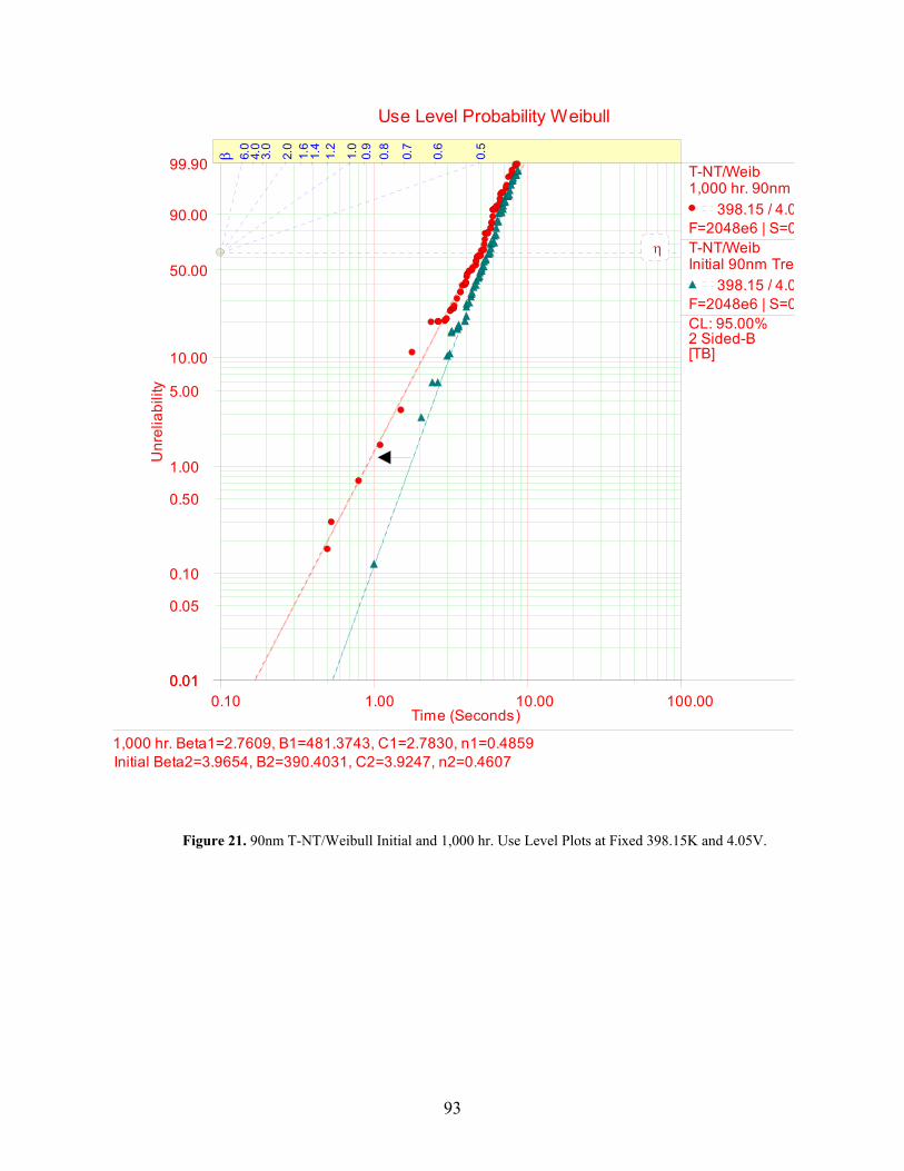
93
Figure 21. 90nm T-NT/Weibull Initial and 1,000 hr. Use Level Plots at Fixed 398.15K and 4.05V.
0.01
0.05
0.10
0.50
1.00
5.00
10.00
50.00
90.00
99.90
0.01
0.5
0.6
0.7
0.8
0.9
1.0
1.2
1.4
1.6
2.0
3.0
4.0
6.0
β
η
0.10 100.001.00 10.00
Use Level Probability Weibull
Time (Seconds)
Unr
elia
bilit
yT-NT/Weib1,000 hr. 90nm
398.15 / 4.0F=2048e6 | S=0T-NT/WeibInitial 90nm Tret
398.15 / 4.0F=2048e6 | S=0CL: 95.00%2 Sided-B[TB]
1,000 hr. Beta1=2.7609, B1=481.3743, C1=2.7830, n1=0.4859Initial Beta2=3.9654, B2=390.4031, C2=3.9247, n2=0.4607
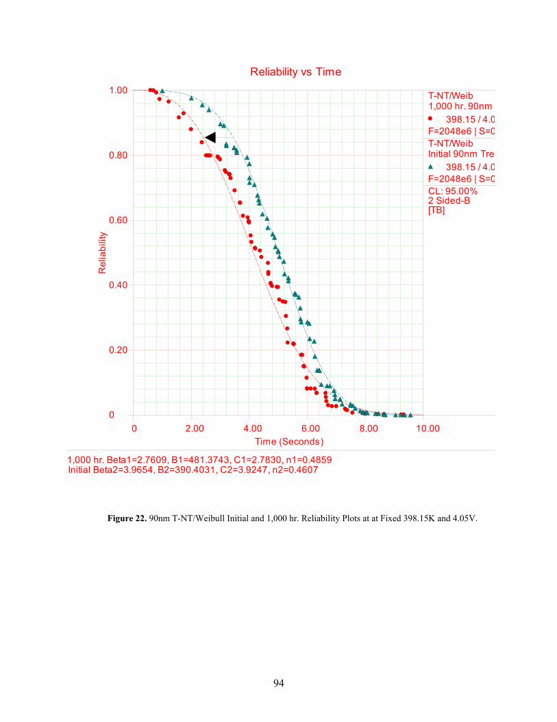
94
Figure 22. 90nm T-NT/Weibull Initial and 1,000 hr. Reliability Plots at at Fixed 398.15K and 4.05V.
0
1.00
0.20
0.40
0.60
0.80
0 10.002.00 4.00 6.00 8.00
Reliability vs Time
Time (Seconds)
Rel
iabi
lity
T-NT/Weib1,000 hr. 90nm
398.15 / 4.0F=2048e6 | S=0T-NT/WeibInitial 90nm Tret
398.15 / 4.0F=2048e6 | S=0CL: 95.00%2 Sided-B[TB]
1,000 hr. Beta1=2.7609, B1=481.3743, C1=2.7830, n1=0.4859Initial Beta2=3.9654, B2=390.4031, C2=3.9247, n2=0.4607
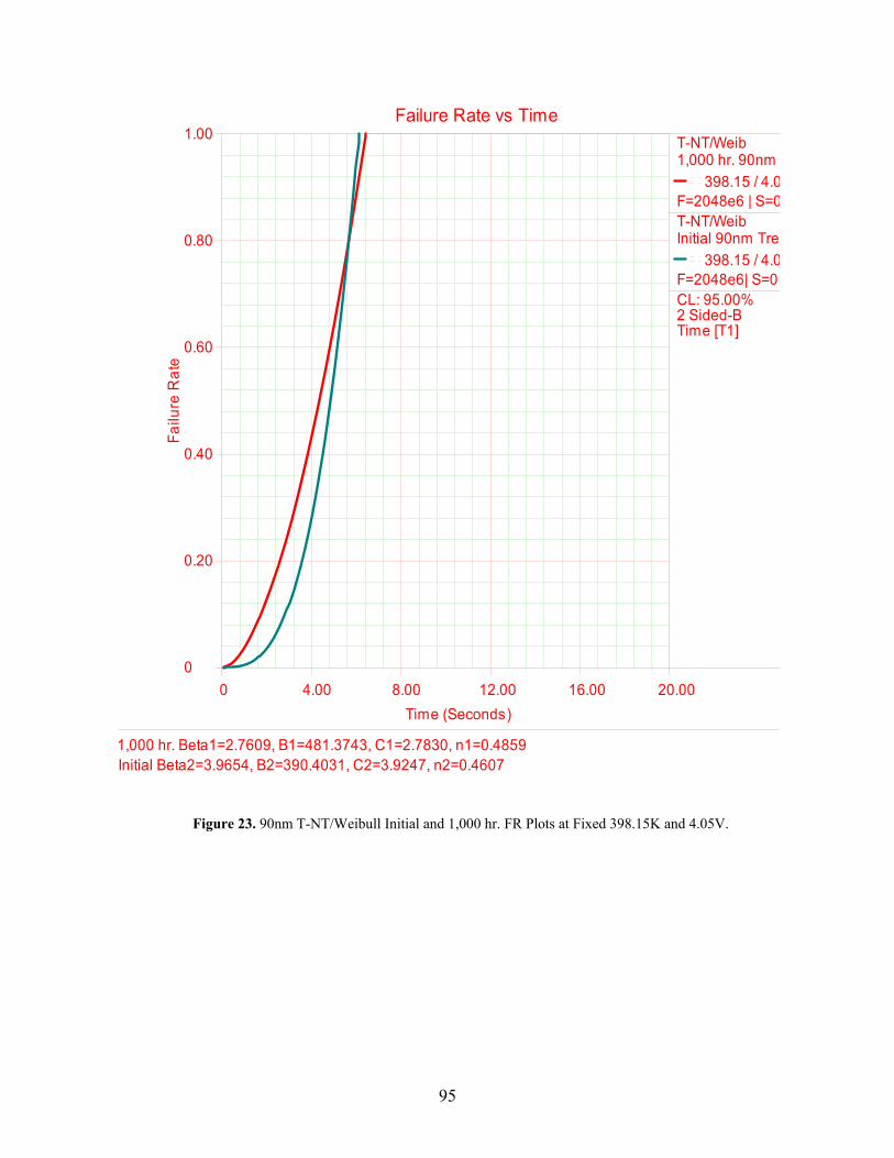
95
Figure 23. 90nm T-NT/Weibull Initial and 1,000 hr. FR Plots at Fixed 398.15K and 4.05V.
0
1.00
0.20
0.40
0.60
0.80
0 20.004.00 8.00 12.00 16.00
Failure Rate vs Time
Time (Seconds)
Failu
re R
ate
T-NT/Weib1,000 hr. 90nm
398.15 / 4.0F=2048e6 | S=0T-NT/WeibInitial 90nm Tret
398.15 / 4.0F=2048e6| S=0CL: 95.00%2 Sided-BTime [T1]
1,000 hr. Beta1=2.7609, B1=481.3743, C1=2.7830, n1=0.4859Initial Beta2=3.9654, B2=390.4031, C2=3.9247, n2=0.4607
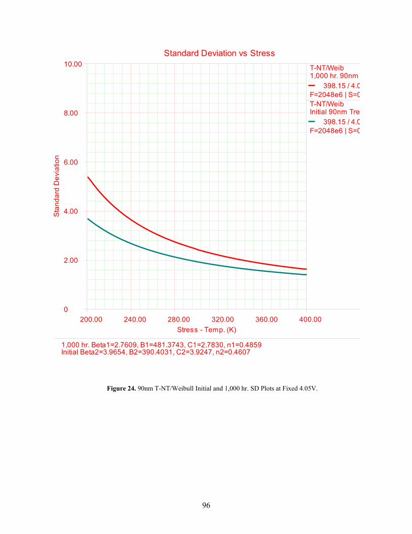
96
Figure 24. 90nm T-NT/Weibull Initial and 1,000 hr. SD Plots at Fixed 4.05V.
0
10.00
2.00
4.00
6.00
8.00
200.00 400.00240.00 280.00 320.00 360.00
Standard Deviation vs Stress
Stress - Temp. (K)
Stan
dard
Dev
iatio
nT-NT/Weib1,000 hr. 90nm
398.15 / 4.0F=2048e6 | S=0T-NT/WeibInitial 90nm Tret
398.15 / 4.0F=2048e6 | S=0
1,000 hr. Beta1=2.7609, B1=481.3743, C1=2.7830, n1=0.4859Initial Beta2=3.9654, B2=390.4031, C2=3.9247, n2=0.4607
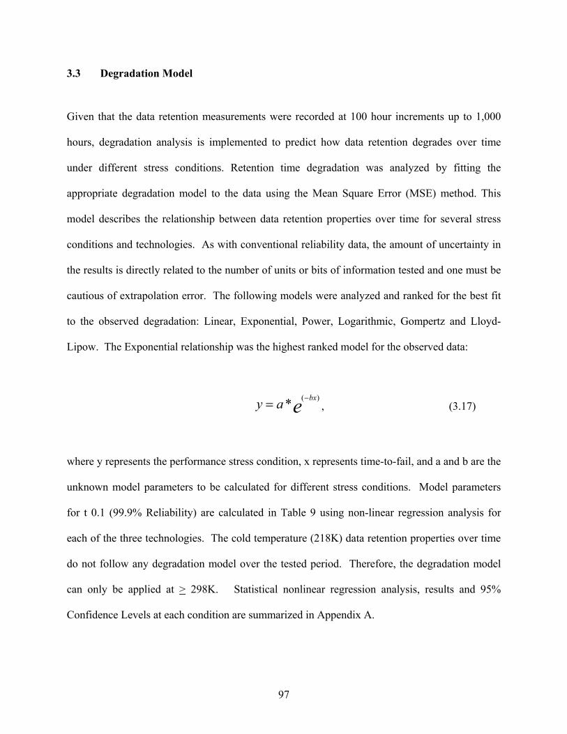
97
3.3 Degradation Model
Given that the data retention measurements were recorded at 100 hour increments up to 1,000
hours, degradation analysis is implemented to predict how data retention degrades over time
under different stress conditions. Retention time degradation was analyzed by fitting the
appropriate degradation model to the data using the Mean Square Error (MSE) method. This
model describes the relationship between data retention properties over time for several stress
conditions and technologies. As with conventional reliability data, the amount of uncertainty in
the results is directly related to the number of units or bits of information tested and one must be
cautious of extrapolation error. The following models were analyzed and ranked for the best fit
to the observed degradation: Linear, Exponential, Power, Logarithmic, Gompertz and Lloyd-
Lipow. The Exponential relationship was the highest ranked model for the observed data:
e bxay )(* −= , (3.17)
where y represents the performance stress condition, x represents time-to-fail, and a and b are the
unknown model parameters to be calculated for different stress conditions. Model parameters
for t 0.1 (99.9% Reliability) are calculated in Table 9 using non-linear regression analysis for
each of the three technologies. The cold temperature (218K) data retention properties over time
do not follow any degradation model over the tested period. Therefore, the degradation model
can only be applied at > 298K. Statistical nonlinear regression analysis, results and 95%
Confidence Levels at each condition are summarized in Appendix A.
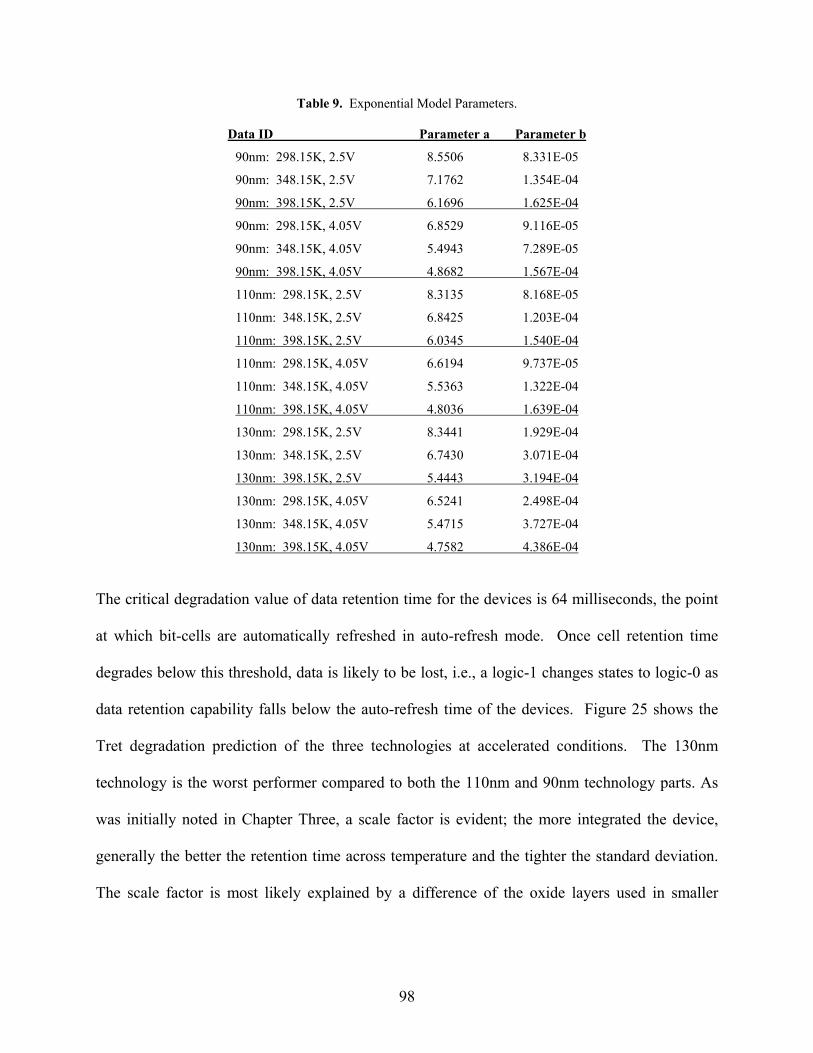
98
Table 9. Exponential Model Parameters.
Data ID Parameter a Parameter b
90nm: 298.15K, 2.5V 8.5506 8.331E-05
90nm: 348.15K, 2.5V 7.1762 1.354E-04
90nm: 398.15K, 2.5V 6.1696 1.625E-04
90nm: 298.15K, 4.05V 6.8529 9.116E-05
90nm: 348.15K, 4.05V 5.4943 7.289E-05
90nm: 398.15K, 4.05V 4.8682 1.567E-04
110nm: 298.15K, 2.5V 8.3135 8.168E-05
110nm: 348.15K, 2.5V 6.8425 1.203E-04
110nm: 398.15K, 2.5V 6.0345 1.540E-04
110nm: 298.15K, 4.05V 6.6194 9.737E-05
110nm: 348.15K, 4.05V 5.5363 1.322E-04
110nm: 398.15K, 4.05V 4.8036 1.639E-04
130nm: 298.15K, 2.5V 8.3441 1.929E-04
130nm: 348.15K, 2.5V 6.7430 3.071E-04
130nm: 398.15K, 2.5V 5.4443 3.194E-04
130nm: 298.15K, 4.05V 6.5241 2.498E-04
130nm: 348.15K, 4.05V 5.4715 3.727E-04
130nm: 398.15K, 4.05V 4.7582 4.386E-04
The critical degradation value of data retention time for the devices is 64 milliseconds, the point
at which bit-cells are automatically refreshed in auto-refresh mode. Once cell retention time
degrades below this threshold, data is likely to be lost, i.e., a logic-1 changes states to logic-0 as
data retention capability falls below the auto-refresh time of the devices. Figure 25 shows the
Tret degradation prediction of the three technologies at accelerated conditions. The 130nm
technology is the worst performer compared to both the 110nm and 90nm technology parts. As
was initially noted in Chapter Three, a scale factor is evident; the more integrated the device,
generally the better the retention time across temperature and the tighter the standard deviation.
The scale factor is most likely explained by a difference of the oxide layers used in smaller
99
technologies (advanced high-K processes) and improvements in cell design, processing and
geometry, i.e., vertical/horizontal staked capacitors, materials, dimensions, etc.
Based on the 64 milliseconds critical threshold and substituting the parameter values into the
Exponential degradation model and solving for x, the t 0.1 time when data retention drops to
99.9% reliability at different stress levels are summarized in Table 10. Times were calculated at
the 95% CL.
Table 10. Data Retention TTF (t 0.1 Point).
Data ID t 0.1 Time-to-Fail (Hours)
90nm: 298.15K, 2.5V 67920.4
90nm: 348.15K, 2.5V 40067.5
90nm: 398.15K, 2.5V 32852.2
90nm: 298.15K, 4.05V 51730.2
90nm: 348.15K, 4.05V 42329.7
90nm: 398.15K, 4.05V 28027.1
110nm: 298.15K, 2.5V 68404.7
110nm: 348.15K, 2.5V 45485.3
110nm: 398.15K, 2.5V 34222.4
110nm: 298.15K, 4.05V 47881.2
110nm: 348.15K, 4.05V 33500.9
110nm: 398.15K, 4.05V 26417.9
130nm: 298.15K, 2.5V 28425.5
130nm: 348.15K, 2.5V 17977.6
130nm: 398.15K, 2.5V 17161.8
130nm: 298.15K, 4.05V 18716.5
130nm: 348.15K, 4.05V 12044.3
130nm: 398.15K, 4.05V 9912.3
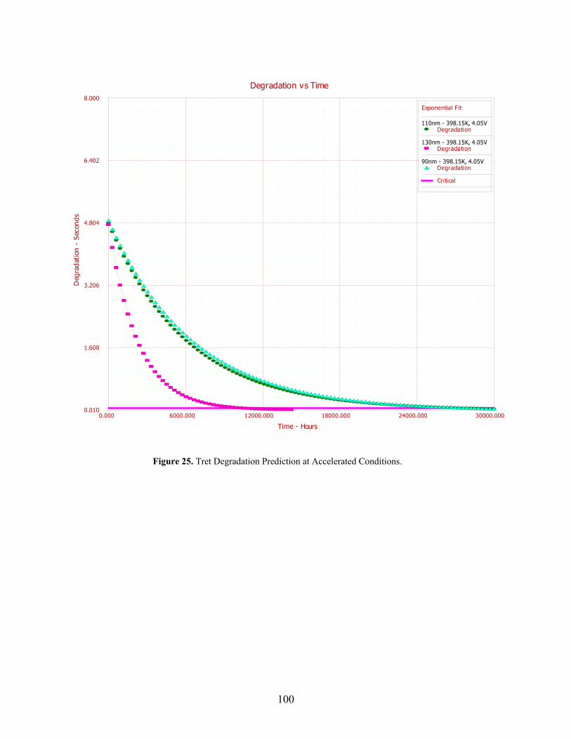
100
Figure 25. Tret Degradation Prediction at Accelerated Conditions.
Degradation vs Time
Time - Hours
Deg
rada
tion
- Se
cond
s
0.000 30000.0006000.000 12000.000 18000.000 24000.0000.010
8.000
1.608
3.206
4.804
6.402
Exponential Fit
110nm - 398.15K, 4.05VDegradation
130nm - 398.15K, 4.05VDegradation
90nm - 398.15K, 4.05VDegradation
Critical
101
Chapter 4: Physics-of-Failure & Systems Approach
4.1 Overview
Retention time margin may also be measured using a Q-ratio of the time-to-first-failure
distribution (t1) to the maximum specified refresh time, (tM). This ratio provides insight into the
tolerance of each technology generation to degradation with respect to voltage and temperature
stresses. The ratio also provides a quality factor demonstrating the amount of margin between
actual soft breakdown and the manufacturer’s specified refresh time. Table 11 shows the (t1)/(tM)
Q-ratios for each technology and stress condition. A high Q-ratio number represents a high
operating margin; a low number represents low margin.
Data retention characteristics are most robust at low temperature, 218K, and nominal operating
voltage, 2.5V. The Q-ratio also reveals that 90nm devices are more robust across the full stress
profile range than the 110nm and 130nm devices. While all three technologies reveal
diminishing margin with increasing temperature and voltage stresses, Table 11 shows that the
temperature component of the stress profile has a greater effect on data retention margin.
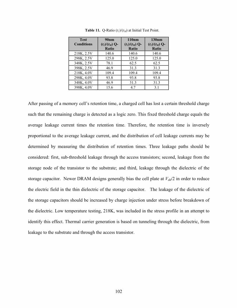
102
Table 11. Q-Ratio (t1)/(tM) at Initial Test Point.
Test Conditions
90nm (t1)/(tM) Q-
Ratio
110nm (t1)/(tM) Q-
Ratio
130nm (t1)/(tM) Q-
Ratio 218K, 2.5V 140.6 140.6 140.6 298K, 2.5V 125.0 125.0 125.0 348K, 2.5V 78.1 62.5 62.5 398K, 2.5V 46.9 31.3 31.3 218K, 4.0V 109.4 109.4 109.4 298K, 4.0V 93.8 93.8 93.8 348K, 4.0V 46.9 31.3 31.3 398K, 4.0V 15.6 4.7 3.1
After passing of a memory cell’s retention time, a charged cell has lost a certain threshold charge
such that the remaining charge is detected as a logic zero. This fixed threshold charge equals the
average leakage current times the retention time. Therefore, the retention time is inversely
proportional to the average leakage current, and the distribution of cell leakage currents may be
determined by measuring the distribution of retention times. Three leakage paths should be
considered: first, sub-threshold leakage through the access transistors; second, leakage from the
storage node of the transistor to the substrate; and third, leakage through the dielectric of the
storage capacitor. Newer DRAM designs generally bias the cell plate at Vdd/2 in order to reduce
the electric field in the thin dielectric of the storage capacitor. The leakage of the dielectric of
the storage capacitors should be increased by charge injection under stress before breakdown of
the dielectric. Low temperature testing, 218K, was included in the stress profile in an attempt to
identify this effect. Thermal carrier generation is based on tunneling through the dielectric, from
leakage to the substrate and through the access transistor.
103
4.2 Failure Mechanisms
The data retention time breakdown failure distributions are similar to the time-to-failure
distributions of the breakdown of thin dielectrics. Therefore, dielectric leakage may be a
precursor to breakdown, and increased through electrical and thermal stresses before breakdown
or other loss of functionality occurs. This effect would show up as a shift in the retention time
distribution measured after stressing the devices. This will be shown graphically later.
The three paths for storage capacitor charge to leak out are through the capacitor dielectric,
through the substrate, and through the transistor channel. The two latter effects on the time to
first-bit failure can be magnified by either increasing or decreasing the substrate bias as was
shown by Shaw et al [106]. For an n-channel transistor, negative substrate biasing decreases the
sub-threshold current exponentially. However, at a very large negative bias, substantial current
may be generated in the depletion region of the storage node’s p-n junction. This current may be
generated by thermal activation of electrons through near mid-gap centers and is proportional to
the depletion width. At temperatures high enough to overcome the full bandgap of silicon,
diffusion of minority carriers may also be a factor. Earlier work shows that a small negative
substrate bias may be generated on-chip, which in effect suppresses both the sub-threshold and
the substrate current [106].
4.3 Discussion
Model distributions were fitted to the failure distributions for each of the technologies studied.
The data supports and fits the Thermal – Non-Thermal (T-NT) Model comprised of the
Arrhenius relationship for the thermal stress, and the Inverse Power Law for the voltage stress.
104
Using this model and the Weibull distribution for plotting, it is shown that the β slope decreases
over time for each stress condition. There are two distinct breakdown failure modes as are
shown in the Weibull distributions in Figures 26 and 27. The first observed breakdown failures
in each distribution appear to be caused by random defects, considered to be extrinsic in nature,
and generally process induced. These failures may be caused by weak areas or defects in the
oxide film, contaminants, fine cracks, or pin holes. Such defects can cause increases in leakage
within the memory cell and early breakdown. The randomness of the defect related first failures
lends itself well for further statistical analysis.
Figure 26 shows that for the 130nm products initial readings at elevated stress conditions,
approximately 0.34% of the early retention time failures are attributable to randomly distributed
weak bits. Similarly, after 1,000 hour stress, Figure 27 shows that at elevated stress conditions a
higher percentage, approximately 0.58% of the early retention time failures, is attributable to
randomly distributed weak bits. At the other end of the spectrum, colder temperature and
nominal operating voltage, the data retention characteristics are much better.
Figure 28 shows that for the 110nm products initial readings at elevated stress conditions,
approximately 0.052% of the early retention time failures are attributable to randomly distributed
weak bits. Similarly, after 1,000 hour stress, Figure 29 shows that at elevated stress conditions a
higher percentage, approximately 0.5% of the early retention time failures, is attributable to
randomly distributed weak bits. Likewise with the 130nm products, at colder temperature and
nominal operating voltage, the data retention characteristics are much better.
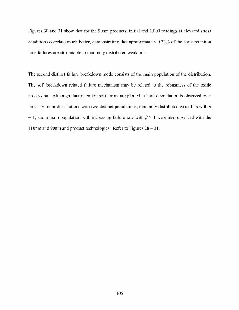
105
Figures 30 and 31 show that for the 90nm products, initial and 1,000 readings at elevated stress
conditions correlate much better, demonstrating that approximately 0.32% of the early retention
time failures are attributable to randomly distributed weak bits.
The second distinct failure breakdown mode consists of the main population of the distribution.
The soft breakdown related failure mechanism may be related to the robustness of the oxide
processing. Although data retention soft errors are plotted, a hard degradation is observed over
time. Similar distributions with two distinct populations, randomly distributed weak bits with β
= 1, and a main population with increasing failure rate with β > 1 were also observed with the
110nm and 90nm and product technologies. Refer to Figures 28 – 31.
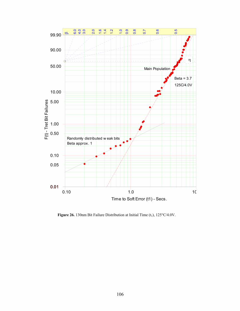
106
Figure 26. 130nm Bit Failure Distribution at Initial Time (t1), 125°C/4.0V.
0.01
0.05
0.10
0.50
1.00
5.00
10.00
50.00
90.00
99.90
0.01
η
0.10 101.0Time to Soft Error (t1) - Secs.
F(t)
- Tre
t Bit
Failu
res
Beta approx. 1Randomly distributed w eak bits
Main Population
0.5
0.6
0.7
0.8
0.9
1.0
1.2
1.4
1.6
2.0
3.0
4.0
6.0
β
Beta = 3.7
125C/4.0V
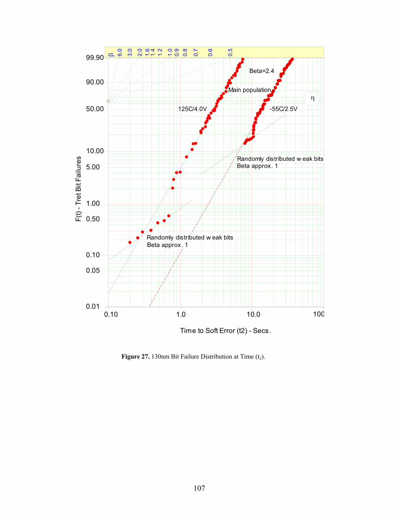
107
Figure 27. 130nm Bit Failure Distribution at Time (t2).
0.01
0.05
0.10
0.50
1.00
5.00
10.00
50.00
90.00
99.90 0.5
0.6
0.7
0.8
0.9
1.0
1.2
1.4
1.6
2.0
3.0
6.0
β
η
0.10 1001.0 10.0
Beta approx. 1
Randomly distributed w eak bits
Time to Soft Error (t2) - Secs.
F(t)
- Tre
t Bit
Failu
res
Main population
125C/4.0V -55C/2.5V
Beta approx. 1
Randomly distributed w eak bits
Beta=2.4
108
Figure 28. 110nm Bit Failure Distribution at Initial Time (t1), 125°C/4.0V.
0.01
0.05
0.10
0.50
1.00
5.00
10.00
50.00
90.00
99.90
0.01
0.5
0.6
0.7
0.8
0.9
1.0
1.2
1.4
1.6
2.0
3.0
4.0
6.0
βη
0.10 101.0
Beta=3.7
Time to Soft Error (t1) - Secs.
F(t)
- Tre
t Bit
Failu
res
Beta approx. 1Randomly distributed w eak bits
Main Population
125C/4.0V
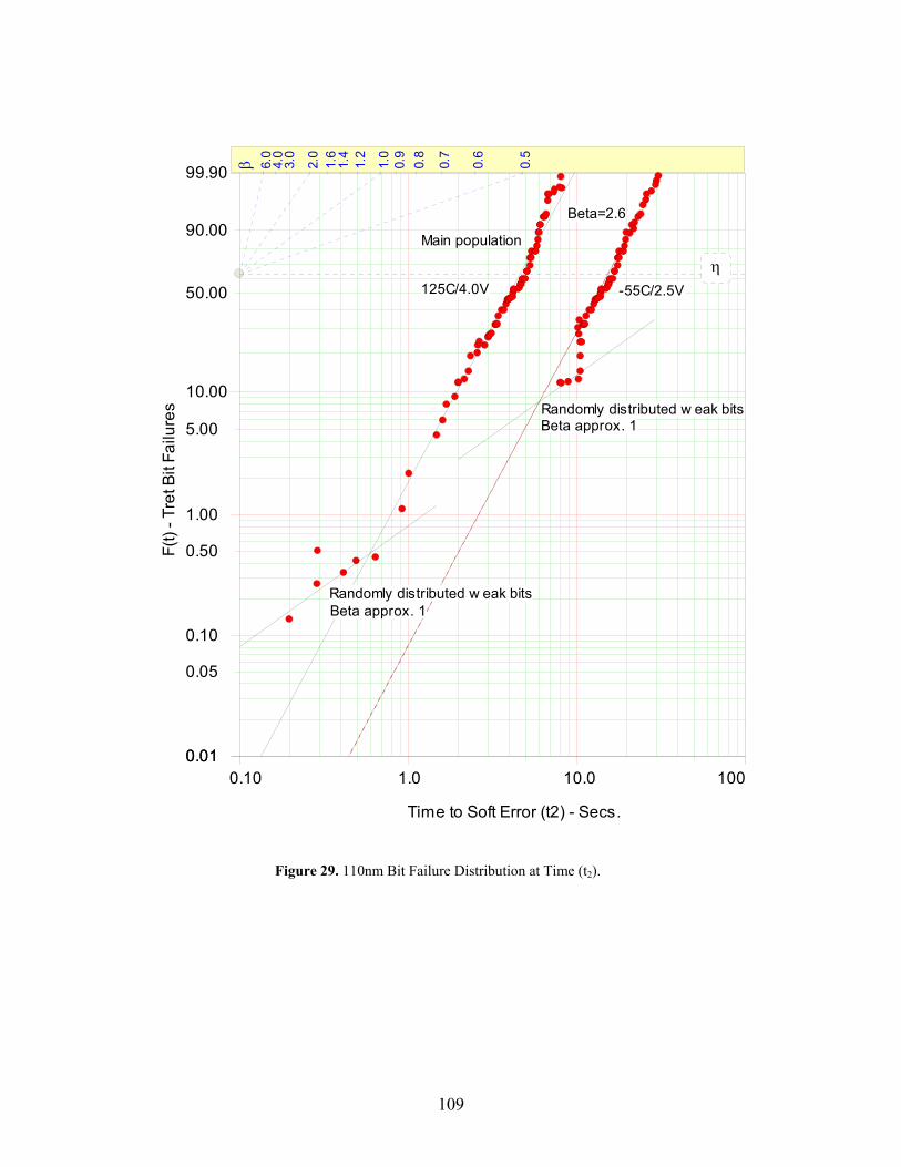
109
Figure 29. 110nm Bit Failure Distribution at Time (t2).
0.01
0.05
0.10
0.50
1.00
5.00
10.00
50.00
90.00
99.90
0.01
0.5
0.6
0.7
0.8
0.9
1.0
1.2
1.4
1.6
2.0
3.0
4.0
6.0
βη
0.10 1001.0 10.0
Beta=2.6
Beta approx. 1
Randomly distributed w eak bits
Time to Soft Error (t2) - Secs.
F(t)
- Tre
t Bit
Failu
res
Main population
125C/4.0V -55C/2.5V
Beta approx. 1
Randomly distributed w eak bits
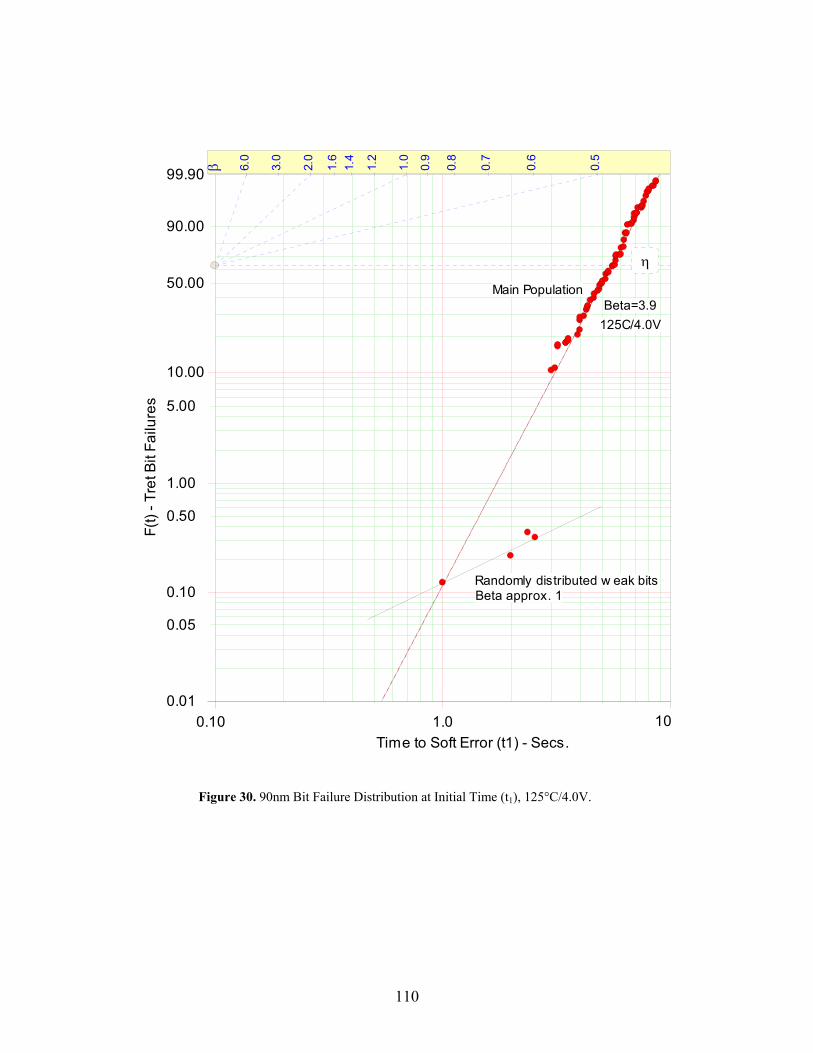
110
Figure 30. 90nm Bit Failure Distribution at Initial Time (t1), 125°C/4.0V.
0.01
0.05
0.10
0.50
1.00
5.00
10.00
50.00
90.00
99.90 0.5
0.6
0.7
0.8
0.9
1.0
1.2
1.4
1.6
2.0
3.0
6.0
β
η
0.10 101.0
Beta=3.9
Time to Soft Error (t1) - Secs.
F(t)
- Tre
t Bit
Failu
res
Beta approx. 1Randomly distributed w eak bits
Main Population
125C/4.0V
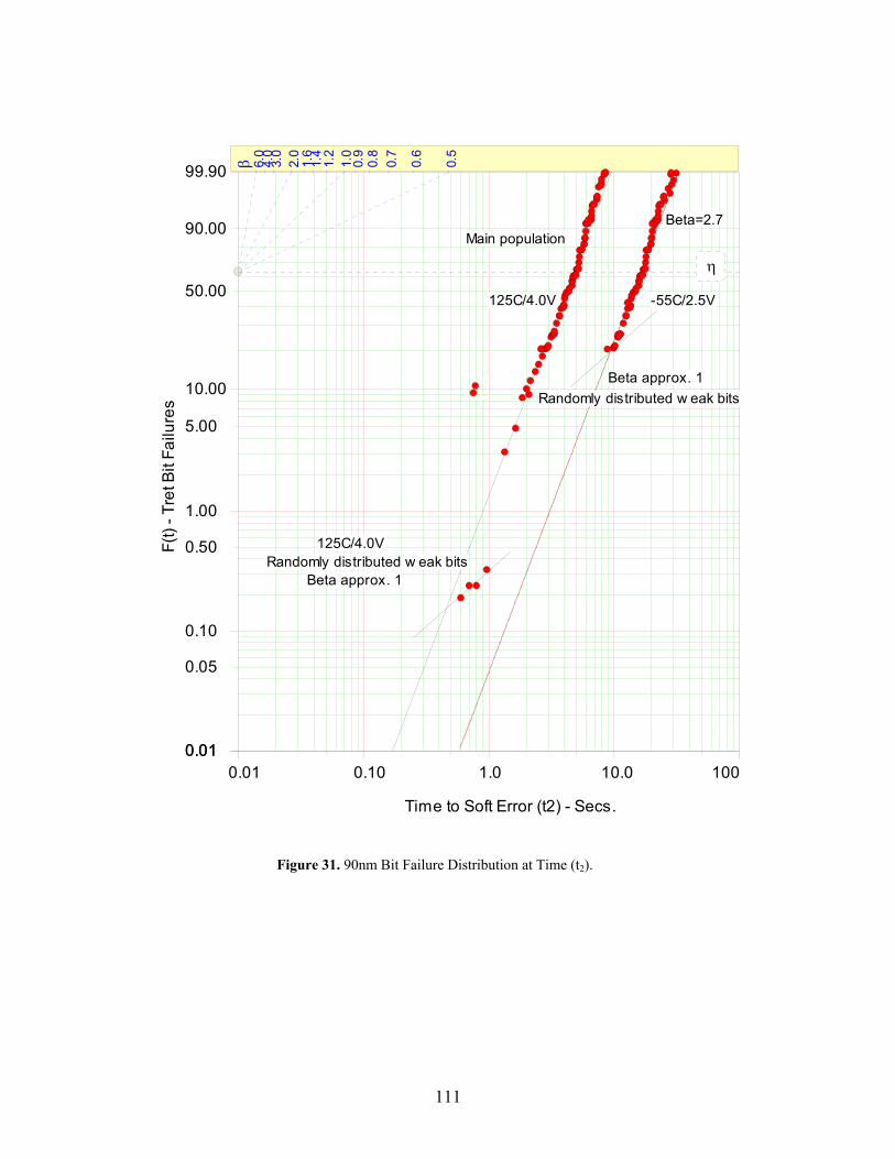
111
Figure 31. 90nm Bit Failure Distribution at Time (t2).
0.01
0.05
0.10
0.50
1.00
5.00
10.00
50.00
90.00
99.90
0.01
0.5
0.6
0.7
0.8
0.9
1.0
1.2
1.4
1.6
2.0
3.0
4.0
6.0
βη
0.01 1000.10 1.0 10.0
Beta approx. 1
Randomly distributed w eak bits
Time to Soft Error (t2) - Secs.
F(t)
- Tre
t Bit
Failu
res
Main population
125C/4.0V
-55C/2.5V
Beta approx. 1
Randomly distributed w eak bits
Beta=2.7
125C/4.0V
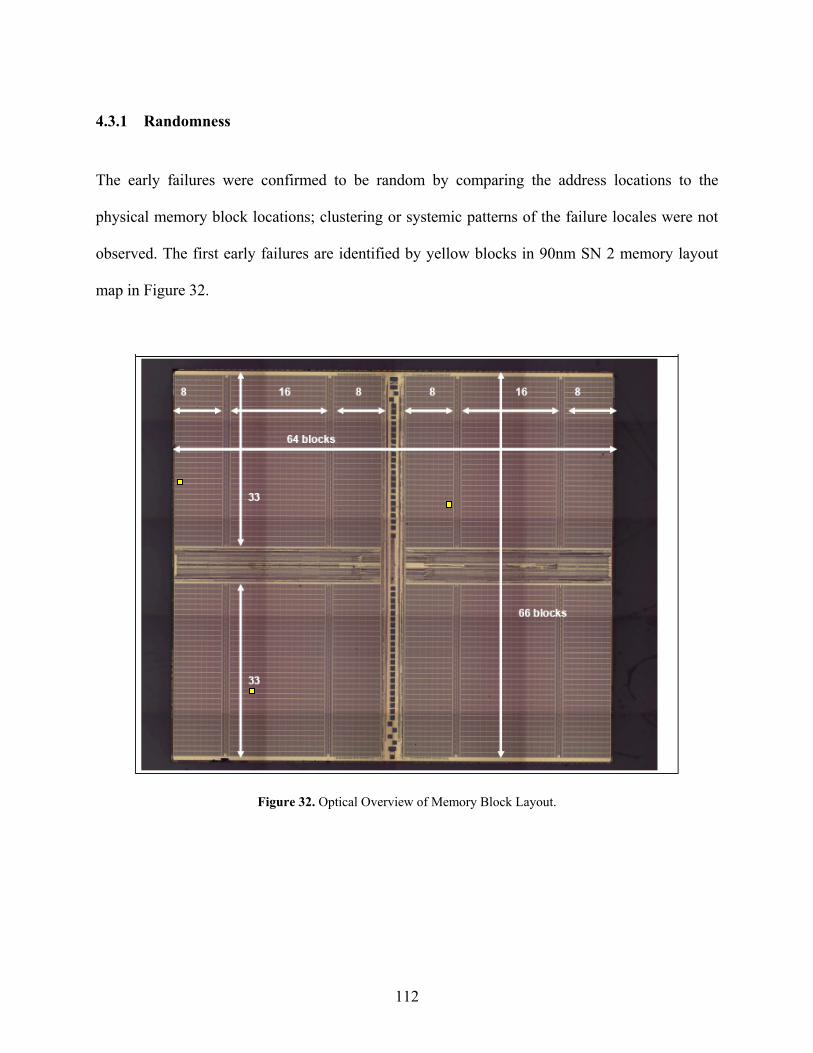
112
4.3.1 Randomness
The early failures were confirmed to be random by comparing the address locations to the
physical memory block locations; clustering or systemic patterns of the failure locales were not
observed. The first early failures are identified by yellow blocks in 90nm SN 2 memory layout
map in Figure 32.
Figure 32. Optical Overview of Memory Block Layout.
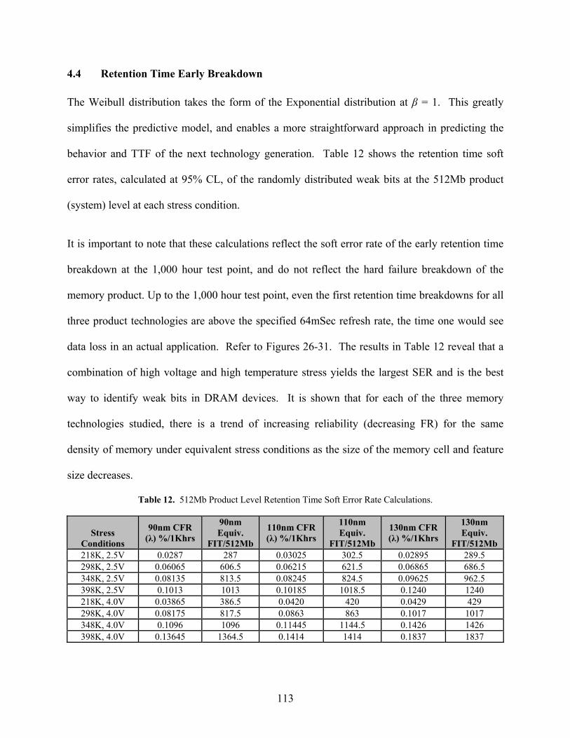
113
4.4 Retention Time Early Breakdown
The Weibull distribution takes the form of the Exponential distribution at β = 1. This greatly
simplifies the predictive model, and enables a more straightforward approach in predicting the
behavior and TTF of the next technology generation. Table 12 shows the retention time soft
error rates, calculated at 95% CL, of the randomly distributed weak bits at the 512Mb product
(system) level at each stress condition.
It is important to note that these calculations reflect the soft error rate of the early retention time
breakdown at the 1,000 hour test point, and do not reflect the hard failure breakdown of the
memory product. Up to the 1,000 hour test point, even the first retention time breakdowns for all
three product technologies are above the specified 64mSec refresh rate, the time one would see
data loss in an actual application. Refer to Figures 26-31. The results in Table 12 reveal that a
combination of high voltage and high temperature stress yields the largest SER and is the best
way to identify weak bits in DRAM devices. It is shown that for each of the three memory
technologies studied, there is a trend of increasing reliability (decreasing FR) for the same
density of memory under equivalent stress conditions as the size of the memory cell and feature
size decreases.
Table 12. 512Mb Product Level Retention Time Soft Error Rate Calculations.
Stress
Conditions
90nm CFR (λ) %/1Khrs
90nm Equiv.
FIT/512Mb
110nm CFR (λ) %/1Khrs
110nm Equiv.
FIT/512Mb
130nm CFR (λ) %/1Khrs
130nm Equiv.
FIT/512Mb 218K, 2.5V 0.0287 287 0.03025 302.5 0.02895 289.5 298K, 2.5V 0.06065 606.5 0.06215 621.5 0.06865 686.5 348K, 2.5V 0.08135 813.5 0.08245 824.5 0.09625 962.5 398K, 2.5V 0.1013 1013 0.10185 1018.5 0.1240 1240 218K, 4.0V 0.03865 386.5 0.0420 420 0.0429 429 298K, 4.0V 0.08175 817.5 0.0863 863 0.1017 1017 348K, 4.0V 0.1096 1096 0.11445 1144.5 0.1426 1426 398K, 4.0V 0.13645 1364.5 0.1414 1414 0.1837 1837
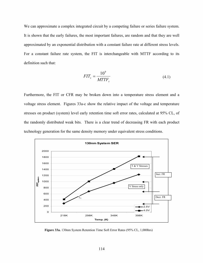
114
We can approximate a complex integrated circuit by a competing failure or series failure system.
It is shown that the early failures, the most important failures, are random and that they are well
approximated by an exponential distribution with a constant failure rate at different stress levels.
For a constant failure rate system, the FIT is interchangeable with MTTF according to its
definition such that:
ss MTTF
FIT910
= (4.1)
Furthermore, the FIT or CFR may be broken down into a temperature stress element and a
voltage stress element. Figures 33a-c show the relative impact of the voltage and temperature
stresses on product (system) level early retention time soft error rates, calculated at 95% CL, of
the randomly distributed weak bits. There is a clear trend of decreasing FR with each product
technology generation for the same density memory under equivalent stress conditions.
Figure 33a. 130nm System Retention Time Soft Error Rates (95% CL, 1,000hrs)
130nm System SER
0
200
400
600
800
1000
1200
1400
1600
1800
2000
218K 298K 348K 398K
Temp. (K)
FIT s
yste
m
2.5V4.0V
TA
T & V Stresses
V Stress only
Incr. FR
Decr. FR
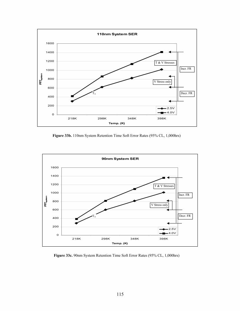
115
Figure 33b. 110nm System Retention Time Soft Error Rates (95% CL, 1,000hrs)
Figure 33c. 90nm System Retention Time Soft Error Rates (95% CL, 1,000hrs)
110nm System SER
0
200
400
600
800
1000
1200
1400
1600
218K 298K 348K 398K
Temp. (K)
FIT s
yste
m
2.5V
4.0V
90nm System SER
0
200
400
600
800
1000
1200
1400
1600
218K 298K 348K 398K
Temp. (K)
FIT s
yste
m
2.5V
4.0V
T & V Stresses
V Stress only
Incr. FR
Decr. FR
T & V Stresses
V Stress only
Incr. FR
Decr. FR
TA
TA
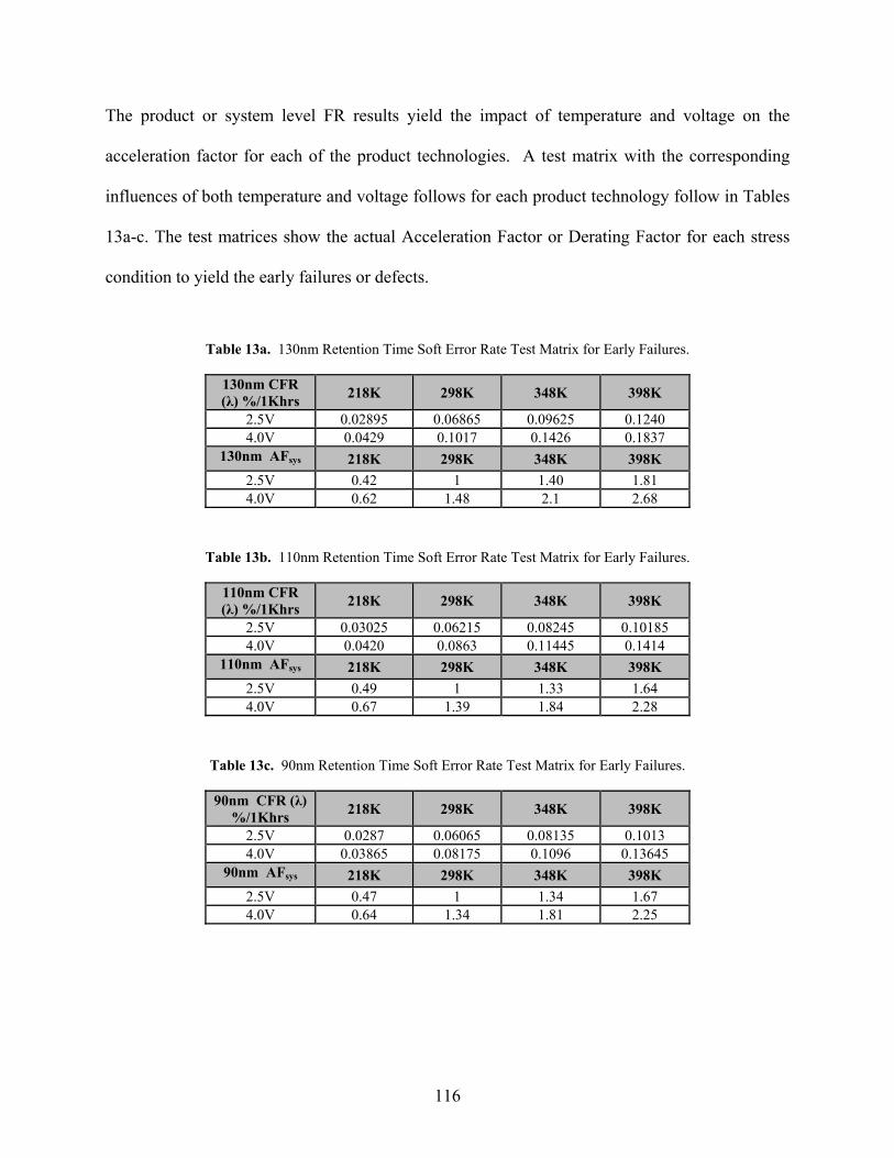
116
The product or system level FR results yield the impact of temperature and voltage on the
acceleration factor for each of the product technologies. A test matrix with the corresponding
influences of both temperature and voltage follows for each product technology follow in Tables
13a-c. The test matrices show the actual Acceleration Factor or Derating Factor for each stress
condition to yield the early failures or defects.
Table 13a. 130nm Retention Time Soft Error Rate Test Matrix for Early Failures.
130nm CFR (λ) %/1Khrs 218K 298K 348K 398K
2.5V 0.02895 0.06865 0.09625 0.1240 4.0V 0.0429 0.1017 0.1426 0.1837
130nm AFsys 218K 298K 348K 398K 2.5V 0.42 1 1.40 1.81 4.0V 0.62 1.48 2.1 2.68
Table 13b. 110nm Retention Time Soft Error Rate Test Matrix for Early Failures.
110nm CFR (λ) %/1Khrs 218K 298K 348K 398K
2.5V 0.03025 0.06215 0.08245 0.10185 4.0V 0.0420 0.0863 0.11445 0.1414
110nm AFsys 218K 298K 348K 398K 2.5V 0.49 1 1.33 1.64 4.0V 0.67 1.39 1.84 2.28
Table 13c. 90nm Retention Time Soft Error Rate Test Matrix for Early Failures.
90nm CFR (λ) %/1Khrs 218K 298K 348K 398K
2.5V 0.0287 0.06065 0.08135 0.1013 4.0V 0.03865 0.08175 0.1096 0.13645
90nm AFsys 218K 298K 348K 398K 2.5V 0.47 1 1.34 1.67 4.0V 0.64 1.34 1.81 2.25
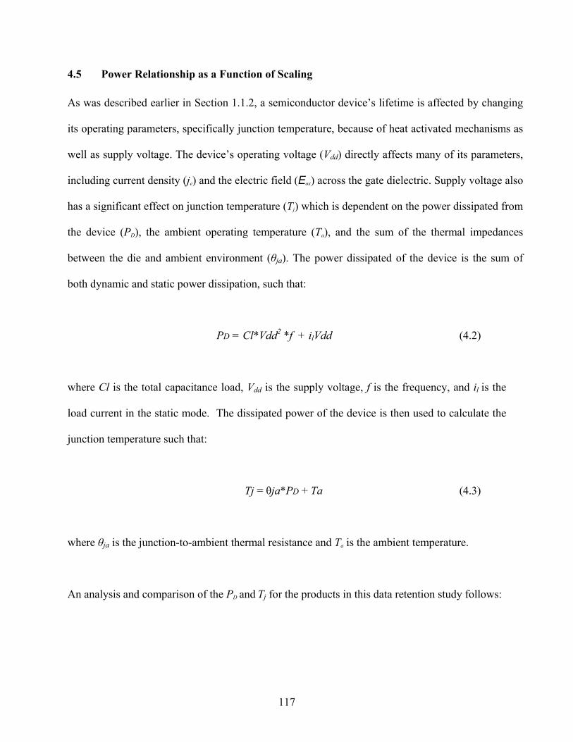
117
4.5 Power Relationship as a Function of Scaling
As was described earlier in Section 1.1.2, a semiconductor device’s lifetime is affected by changing
its operating parameters, specifically junction temperature, because of heat activated mechanisms as
well as supply voltage. The device’s operating voltage (Vdd) directly affects many of its parameters,
including current density (je) and the electric field (Eox) across the gate dielectric. Supply voltage also
has a significant effect on junction temperature (Tj) which is dependent on the power dissipated from
the device (PD), the ambient operating temperature (Ta), and the sum of the thermal impedances
between the die and ambient environment (θja). The power dissipated of the device is the sum of
both dynamic and static power dissipation, such that:
PD = Cl*Vdd2 *f + ilVdd (4.2)
where Cl is the total capacitance load, Vdd is the supply voltage, f is the frequency, and il is the
load current in the static mode. The dissipated power of the device is then used to calculate the
junction temperature such that:
Tj = θja*PD + Ta (4.3)
where θja is the junction-to-ambient thermal resistance and Ta is the ambient temperature.
An analysis and comparison of the PD and Tj for the products in this data retention study follows:
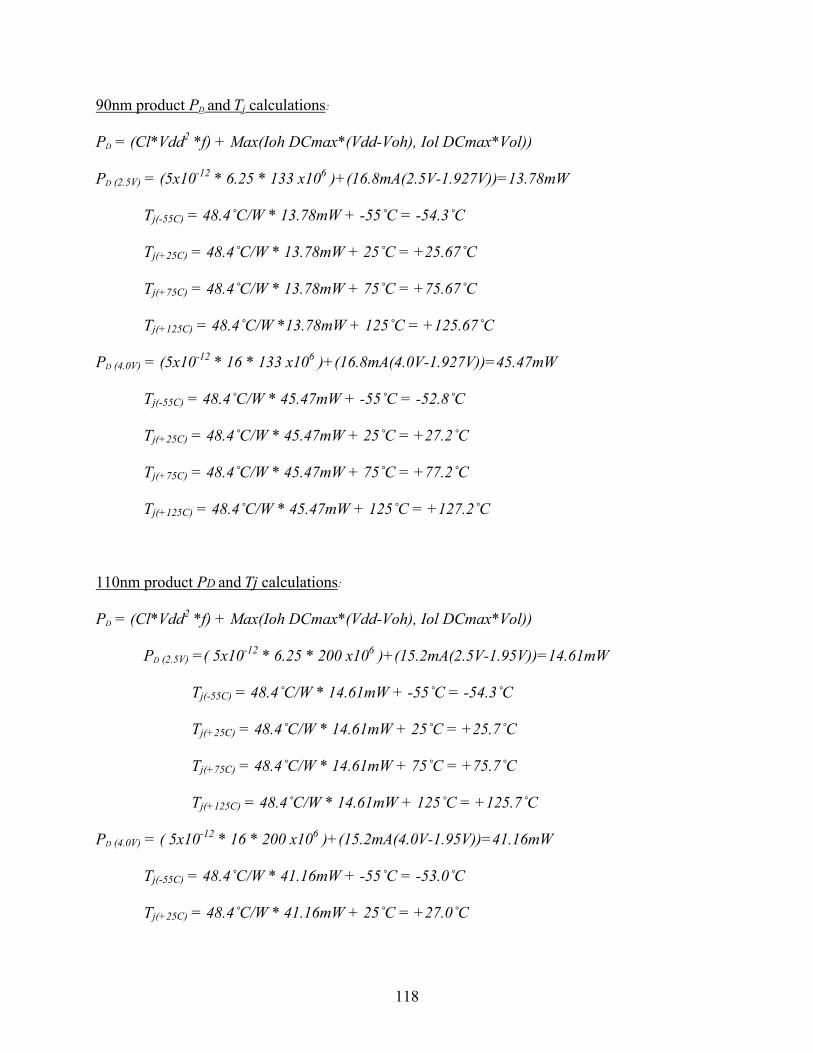
118
90nm product PD and Tj calculations:
PD = (Cl*Vdd2 *f) + Max(Ioh DCmax*(Vdd-Voh), Iol DCmax*Vol))
PD (2.5V) = (5x10-12 * 6.25 * 133 x106 )+(16.8mA(2.5V-1.927V))=13.78mW
Tj(-55C) = 48.4˚C/W * 13.78mW + -55˚C = -54.3˚C
Tj(+25C) = 48.4˚C/W * 13.78mW + 25˚C = +25.67˚C
Tj(+75C) = 48.4˚C/W * 13.78mW + 75˚C = +75.67˚C
Tj(+125C) = 48.4˚C/W *13.78mW + 125˚C = +125.67˚C
PD (4.0V) = (5x10-12 * 16 * 133 x106 )+(16.8mA(4.0V-1.927V))=45.47mW
Tj(-55C) = 48.4˚C/W * 45.47mW + -55˚C = -52.8˚C
Tj(+25C) = 48.4˚C/W * 45.47mW + 25˚C = +27.2˚C
Tj(+75C) = 48.4˚C/W * 45.47mW + 75˚C = +77.2˚C
Tj(+125C) = 48.4˚C/W * 45.47mW + 125˚C = +127.2˚C
110nm product PD and Tj calculations:
PD = (Cl*Vdd2 *f) + Max(Ioh DCmax*(Vdd-Voh), Iol DCmax*Vol))
PD (2.5V) =( 5x10-12 * 6.25 * 200 x106 )+(15.2mA(2.5V-1.95V))=14.61mW
Tj(-55C) = 48.4˚C/W * 14.61mW + -55˚C = -54.3˚C
Tj(+25C) = 48.4˚C/W * 14.61mW + 25˚C = +25.7˚C
Tj(+75C) = 48.4˚C/W * 14.61mW + 75˚C = +75.7˚C
Tj(+125C) = 48.4˚C/W * 14.61mW + 125˚C = +125.7˚C
PD (4.0V) = ( 5x10-12 * 16 * 200 x106 )+(15.2mA(4.0V-1.95V))=41.16mW
Tj(-55C) = 48.4˚C/W * 41.16mW + -55˚C = -53.0˚C
Tj(+25C) = 48.4˚C/W * 41.16mW + 25˚C = +27.0˚C
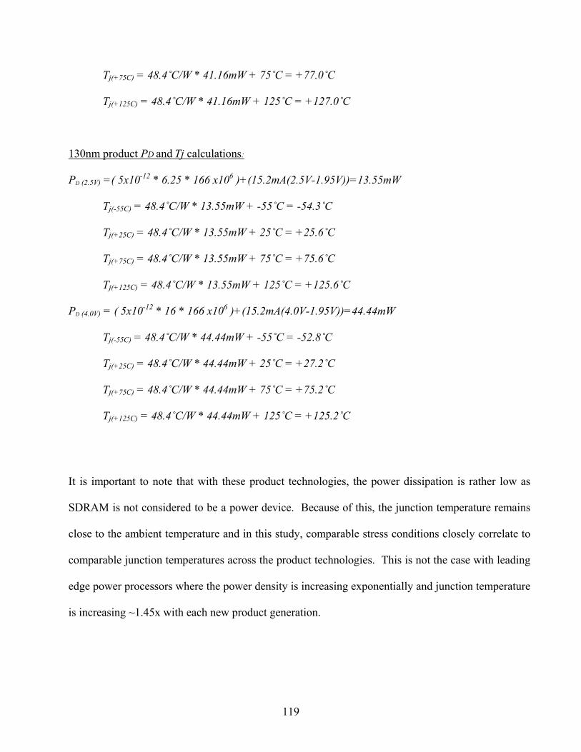
119
Tj(+75C) = 48.4˚C/W * 41.16mW + 75˚C = +77.0˚C
Tj(+125C) = 48.4˚C/W * 41.16mW + 125˚C = +127.0˚C
130nm product PD and Tj calculations:
PD (2.5V) =( 5x10-12 * 6.25 * 166 x106 )+(15.2mA(2.5V-1.95V))=13.55mW
Tj(-55C) = 48.4˚C/W * 13.55mW + -55˚C = -54.3˚C
Tj(+25C) = 48.4˚C/W * 13.55mW + 25˚C = +25.6˚C
Tj(+75C) = 48.4˚C/W * 13.55mW + 75˚C = +75.6˚C
Tj(+125C) = 48.4˚C/W * 13.55mW + 125˚C = +125.6˚C
PD (4.0V) = ( 5x10-12 * 16 * 166 x106 )+(15.2mA(4.0V-1.95V))=44.44mW
Tj(-55C) = 48.4˚C/W * 44.44mW + -55˚C = -52.8˚C
Tj(+25C) = 48.4˚C/W * 44.44mW + 25˚C = +27.2˚C
Tj(+75C) = 48.4˚C/W * 44.44mW + 75˚C = +75.2˚C
Tj(+125C) = 48.4˚C/W * 44.44mW + 125˚C = +125.2˚C
It is important to note that with these product technologies, the power dissipation is rather low as
SDRAM is not considered to be a power device. Because of this, the junction temperature remains
close to the ambient temperature and in this study, comparable stress conditions closely correlate to
comparable junction temperatures across the product technologies. This is not the case with leading
edge power processors where the power density is increasing exponentially and junction temperature
is increasing ~1.45x with each new product generation.
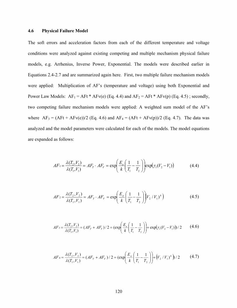
120
4.6 Physical Failure Model
The soft errors and acceleration factors from each of the different temperature and voltage
conditions were analyzed against existing competing and multiple mechanism physical failure
models, e.g. Arrhenius, Inverse Power, Exponential. The models were described earlier in
Equations 2.4-2.7 and are summarized again here. First, two multiple failure mechanism models
were applied: Multiplication of AF’s (temperature and voltage) using both Exponential and
Power Law Models: AF1 = AFt * AFv(e) (Eq. 4.4) and AF2 = AFt * AFv(p) (Eq. 4.5) ; secondly,
two competing failure mechanism models were applied: A weighted sum model of the AF’s
where AF3 = (AFt + AFv(e))/2 (Eq. 4.6) and AF4 = (AFt + AFv(p))/2 (Eq. 4.7). The data was
analyzed and the model parameters were calculated for each of the models. The model equations
are expanded as follows:
( ))(exp11exp),(),(
1212111
221 VVTTk
EAFAFVTVTAF a
VT −⎟⎟⎠
⎞⎜⎜⎝
⎛⎟⎟⎠
⎞⎜⎜⎝
⎛−=⋅== γ
λλ (4.4)
( )kaVT VV
TTkE
AFAFVTVT
AF )/11exp),(),(
122111
222 ⎟
⎟⎠
⎞⎜⎜⎝
⎛⎟⎟⎠
⎞⎜⎜⎝
⎛−=⋅==
λλ (4.5)
( ) 2/))(exp11(exp2/)(),(),(
1212111
223 VVTTk
EAFAFVTVTAF a
VT −+⎟⎟⎠
⎞⎜⎜⎝
⎛⎟⎟⎠
⎞⎜⎜⎝
⎛−=+== γ
λλ
(4.6)
( ) 2/))/11(exp2/)(),(),(
122111
224
kaVT VV
TTkE
AFAFVTVT
AF +⎟⎟⎠
⎞⎜⎜⎝
⎛⎟⎟⎠
⎞⎜⎜⎝
⎛−=+==
λλ (4.7)
121
The calculated Ea, γ, and k parameters are as follows:
Ea for 130nm = 0.06
Ea for 110nm = 0.05
Ea for 90nm = 0.052
Applying the Power Law model for AFv, the derived k for each technology node is:
k for 130nm: 0.84
k for 110nm: 0.693
k for 90nm: 0.637
Applying the Exponential model for AFv, the derived γ for each technology node is:
γ for 130nm: 0.263
γ for 110nm: 0.216
γ for 130nm: 0.1997
The multiple failure mechanism acceleration model, refer to Equation 4.5 (product of AF's using
the Power Law for AFv) best fits the DRAM retention time data and suggests a single
temperature and voltage activated breakdown mechanism. The relative contribution of T and V
on the system level FR is shown pictorially in Figures 33a-c. The thermal element is the main
contributor to Tret breakdown degradation, the voltage element contributes to the thermally
activated mechanism by slightly increasing the junction temperature.
122
As was discussed earlier, for current generation DRAM, the capacitance is typically 30-40fF/cell
and although the external power supply Vdd is 2.5V for each part, internal on-chip voltage
regulator circuitry subdivides this voltage as follows:
130nm Technology Parts:
- Peripheral Circuitry Voltage: 2.2V
- Memory Core Voltage: 1.8V
110nm Technology Parts:
- Peripheral Circuitry Voltage: 1.8V
- Memory Core Voltage: 1.4V
90nm Technology Parts:
- Peripheral Circuitry Voltage: 1.4V
- Memory Core Voltage: 1.0V
The memory cell capacitor dielectric material is Ta2O5. The gate oxide thickness for the larger
peripheral circuitry transistors is approximately 7nm, and the gate oxide thickness for the nMOS
memory cell transistors is approximately 4.2 nm.
Due to the over-voltage protection circuitry in each of the products, higher Vdd stress is not
applied directly to the memory cores and this voltage is maintained at the specified amount.
Therefore, the impact of higher Vdd stress corresponds to an increase in power dissipation for
each of the products; these are summarized Section 5.5. There is no feasible method of
bypassing the over-voltage protection at the product level for product level testing; however, it is

123
important to see the overall impact has on the overall product level power dissipation and
contribution to the product, or system level FR.
The activation energies are very small for the early retention time breakdown errors, up to the
1,000 hour test measurement. As for the entire population of Tret breakdown, the activation
energies are in the same range. Refer to Tables 13a and 13b. The slow degradation of Tret over
time and the low activation energies suggest that hot carrier injection may be the intrinsic
wearout mechanism at work.
The switching characteristics of a MOSFET can degrade and exhibit instabilities due to the
charge that is injected into the gate oxide. The typical effect of hot carrier, or hot electron
degradation, is an increase in the off-state current of a p-channel MOSFET, and a reduction in
the on-state current of an n-channel MOSFET, e.g., those that comprise each memory cell. The
rate of hot carrier degradation is directly related to the length of the channel, the oxide thickness,
and the voltage of the device. A measure of transistor degradation or lifetime is commonly
defined in terms of percentage shift of threshold voltage, change in transconductance, or
variation in drive or saturation current [71]. These parameter shifts, however, were not
confirmed in this experiment.
Gradual time-dependent dielectric breakdown of the DRAM stacked storage capacitor cell is
another possible intrinsic wearout mechanism explanation. The stacked capacitor cell (STC)
relies heavily on the quality and the storage capacity of the dielectric film between two heavily
doped polysilicon electrodes. Silicon nitride (Si3N4) films have a high dielectric constant and are
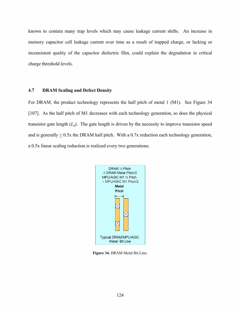
124
known to contain many trap levels which may cause leakage current shifts. An increase in
memory capacitor cell leakage current over time as a result of trapped charge, or lacking or
inconsistent quality of the capacitor dielectric film, could explain the degradation in critical
charge threshold levels.
4.7 DRAM Scaling and Defect Density
For DRAM, the product technology represents the half pitch of metal 1 (M1). See Figure 34
[107]. As the half pitch of M1 decreases with each technology generation, so does the physical
transistor gate length (Lg). The gate length is driven by the necessity to improve transistor speed
and is generally < 0.5x the DRAM half pitch. With a 0.7x reduction each technology generation,
a 0.5x linear scaling reduction is realized every two generations.
Figure 34. DRAM Metal Bit Line.
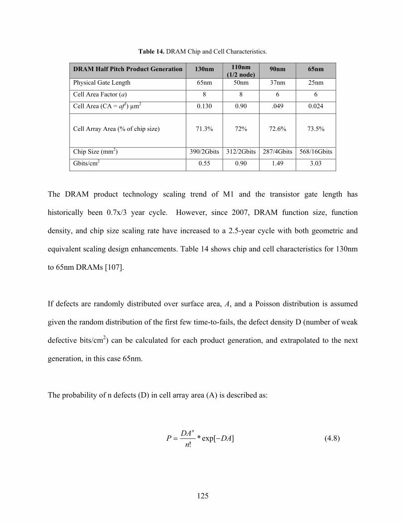
125
Table 14. DRAM Chip and Cell Characteristics.
DRAM Half Pitch Product Generation 130nm 110nm (1/2 node)
90nm 65nm
Physical Gate Length 65nm 50nm 37nm 25nm
Cell Area Factor (a) 8 8 6 6
Cell Area (CA = af2) µm2 0.130 0.90 .049 0.024
Cell Array Area (% of chip size) 71.3% 72% 72.6% 73.5%
Chip Size (mm2) 390/2Gbits 312/2Gbits 287/4Gbits 568/16Gbits
Gbits/cm2 0.55 0.90 1.49 3.03
The DRAM product technology scaling trend of M1 and the transistor gate length has
historically been 0.7x/3 year cycle. However, since 2007, DRAM function size, function
density, and chip size scaling rate have increased to a 2.5-year cycle with both geometric and
equivalent scaling design enhancements. Table 14 shows chip and cell characteristics for 130nm
to 65nm DRAMs [107].
If defects are randomly distributed over surface area, A, and a Poisson distribution is assumed
given the random distribution of the first few time-to-fails, the defect density D (number of weak
defective bits/cm2) can be calculated for each product generation, and extrapolated to the next
generation, in this case 65nm.
The probability of n defects (D) in cell array area (A) is described as:
]exp[*!
DAn
DAPn
−= (4.8)
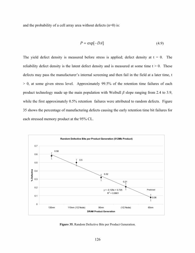
126
and the probability of a cell array area without defects (n=0) is:
]exp[ DAP −= (4.9)
The yield defect density is measured before stress is applied; defect density at t = 0. The
reliability defect density is the latent defect density and is measured at some time t > 0. These
defects may pass the manufacturer’s internal screening and then fail in the field at a later time, t
> 0, at some given stress level. Approximately 99.5% of the retention time failures of each
product technology made up the main population with Weibull β slope ranging from 2.4 to 3.9,
while the first approximately 0.5% retention failures were attributed to random defects. Figure
35 shows the percentage of manufacturing defects causing the early retention time bit failures for
each stressed memory product at the 95% CL.
Figure 35. Random Defective Bits per Product Generation.
Random Defective Bits per Product Generation (512Mb Product)
0.08
0.21
0.5
0.58
0.32
y = -0.129x + 0.725R2 = 0.9901
0
0.1
0.2
0.3
0.4
0.5
0.6
0.7
130nm 110nm (1/2 Node) 90nm (1/2 Node) 65nm
DRAM Product Generation
% D
efec
tive
Predicted
127
Observed 512Mb, 130nm product technology: 0.58% random defective bits
Observed 512Mb, 110nm product technology: 0.50% random defective bits
Observed 512Mb, 90nm product technology: 0.32% random defective bits
Predicted 512Mb, 65nm product technology: 0.08% random defective bits
Each smaller technology generation exhibited fewer random defects than the previous
generation. Trend analysis predicts the next technology generation, 65nm, to exhibit 0.08%
random defective bits assuming the trend continues. Given the option between a 512Mb 130nm
product and a 512Mb 65nm product under equivalent stress conditions, the data suggests the
512Mb 65nm product will have fewer defects. This trend is likely to continue due to tighter
process controls needed for smaller geometries, and the desire to maintain constant product level
failure rates for ever increasing Gb size memory products.
In actuality, with each new product generation and a 2x bit factor for each progressive full node,
the standard DRAM product size at the 65nm node is no longer 512 Mbits, but 8 Gbits. Given
this trend, the random number of defective bits per cm2 must also be considered.
By incorporating the defect rates for each representative technology and the cell characteristics
in Table 14, the defect density per cm2 of DRAM memory is calculated as follows:
130nm product generation: DD = 3.19x106 bits/cm2 (0.55 Gb)
110nm product generation: DD = 4.5x106 bits/cm2 (0.90 Gb)
90nm product generation: DD = 4.768x106 bits/cm2 (1.49 Gb)
128
Using the predicted random defective bits with the cell characteristics of the 65nm DRAM, the
defect density per Gbit of DRAM for the next product generation is:
Predicted 65nm product generation: DD = 2.424 x106 bits/cm2 (3.03 Gb)
Note that while there is only a marginal increase in defect density per cm2 per DRAM generation
(130nm to 90nm), the number of Gbits of memory per cm2 per DRAM generation is increasing
significantly. The 65nm DRAM standard product contains 8 Gbits of memory. Therefore,
normalizing the defect density to the standard products, the 512Mb 130nm standard product had
2.9696 x 10⁶ weak bits and an 8 Gbit 65nm product is expected to have 6.5536 x 10⁶ weak bits.
A 16x increase in memory size from a 130nm 512Mb standard product to an 8 Gbit 65nm
product, corresponds to a disproportional 2.2x increase in defective weak bits, a much better
product in terms of proportion of weak bits.
4.8 Soft Error Failure Rate
The defect density and the soft error failure rate of the random bits must be considered in tandem
to effectively assess the quality and the reliability of the scaled products. Data was normalized
to FIT/Gb of memory and analyses of the soft error failure rate of the random bits are presented
in Figure 36 and Table 15. The graph shows how the soft error failure rate of retention time
behaves for scaled DRAM at multiple stress conditions. Curves were fit to the data which reveal
a power relationship as a function of scaling for the higher stresses, > 348K and 2.5V, or > 298K
and 4.0V; a linear relationship exists for lower stress levels across product generations, e.g., <
298K and 2.5V, or < 218K and 4.0V. The lowest failure rates across product generations is
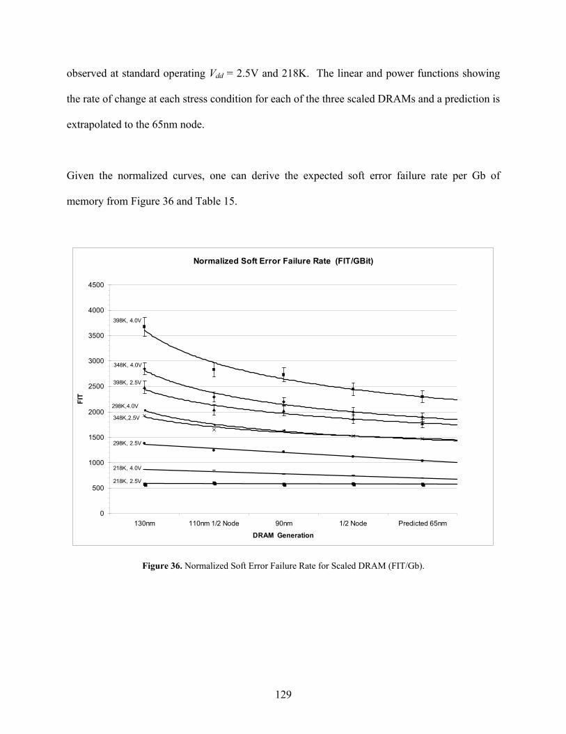
129
observed at standard operating Vdd = 2.5V and 218K. The linear and power functions showing
the rate of change at each stress condition for each of the three scaled DRAMs and a prediction is
extrapolated to the 65nm node.
Given the normalized curves, one can derive the expected soft error failure rate per Gb of
memory from Figure 36 and Table 15.
Figure 36. Normalized Soft Error Failure Rate for Scaled DRAM (FIT/Gb).
Normalized Soft Error Failure Rate (FIT/GBit)
0
500
1000
1500
2000
2500
3000
3500
4000
4500
130nm 110nm 1/2 Node 90nm 1/2 Node Predicted 65nm
DRAM Generation
FIT
218K, 4.0V
298K, 2.5V
348K,2.5V
298K,4.0V
218K, 2.5V
398K, 2.5V
348K, 4.0V
398K, 4.0V
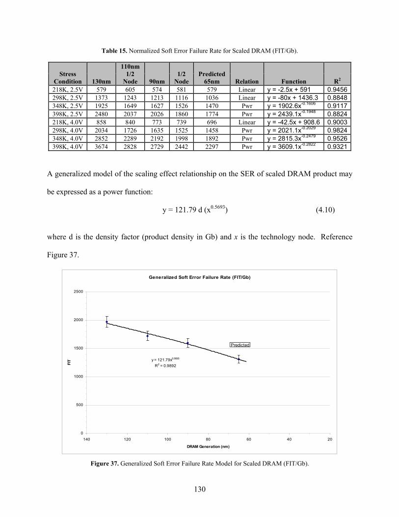
130
Table 15. Normalized Soft Error Failure Rate for Scaled DRAM (FIT/Gb).
Stress Condition 130nm
110nm 1/2
Node 90nm 1/2
Node Predicted
65nm Relation Function R2 218K, 2.5V 579 605 574 581 579 Linear y = -2.5x + 591 0.9456298K, 2.5V 1373 1243 1213 1116 1036 Linear y = -80x + 1436.3 0.8848348K, 2.5V 1925 1649 1627 1526 1470 Pwr y = 1902.6x-0.1606 0.9117398K, 2.5V 2480 2037 2026 1860 1774 Pwr y = 2439.1x-0.1948 0.8824218K, 4.0V 858 840 773 739 696 Linear y = -42.5x + 908.6 0.9003298K, 4.0V 2034 1726 1635 1525 1458 Pwr y = 2021.1x-0.2029 0.9824348K, 4.0V 2852 2289 2192 1998 1892 Pwr y = 2815.3x-0.2479 0.9526398K, 4.0V 3674 2828 2729 2442 2297 Pwr y = 3609.1x-0.2822 0.9321
A generalized model of the scaling effect relationship on the SER of scaled DRAM product may
be expressed as a power function:
y = 121.79 d (x0.5693) (4.10)
where d is the density factor (product density in Gb) and x is the technology node. Reference
Figure 37.
Figure 37. Generalized Soft Error Failure Rate Model for Scaled DRAM (FIT/Gb).
Generalized Soft Error Failure Rate (FIT/Gb)
y = 121.79x0.5693
R2 = 0.9892
0
500
1000
1500
2000
2500
20406080100120140
DRAM Generation (nm)
FIT
Predicted
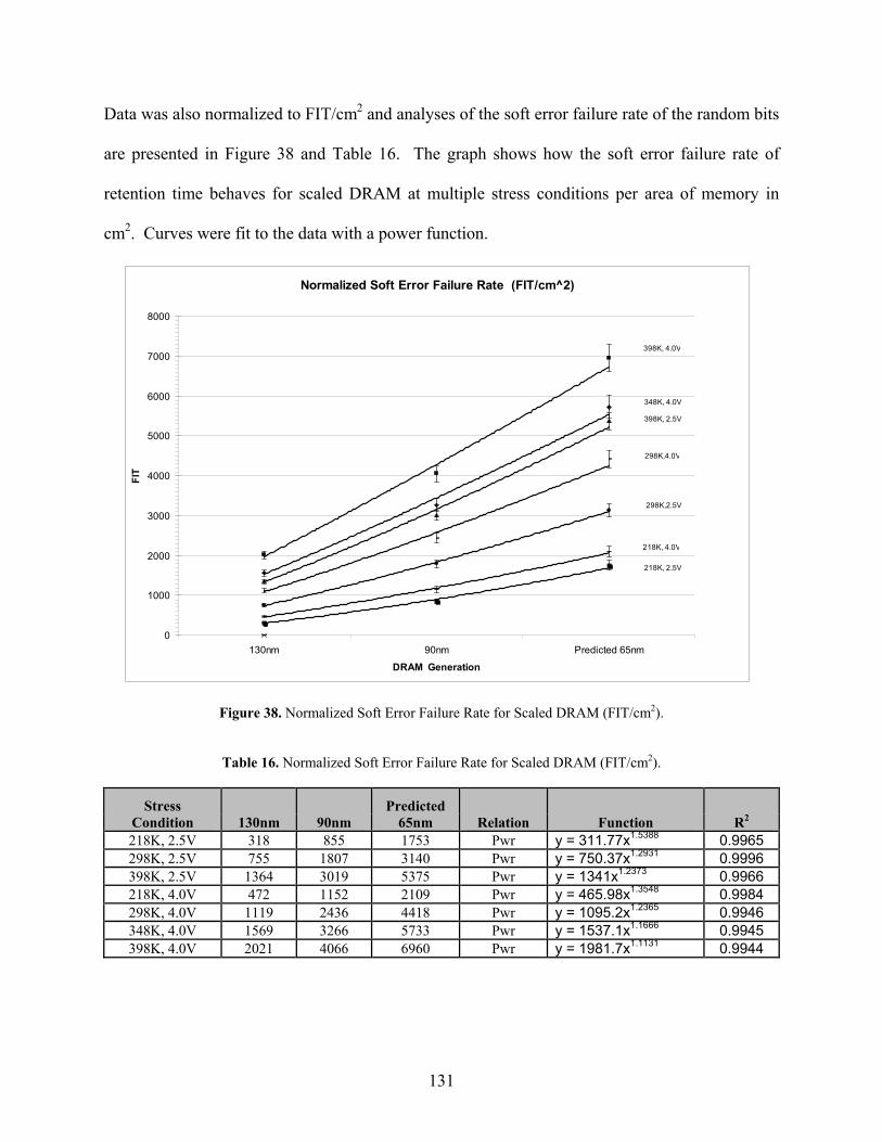
131
Data was also normalized to FIT/cm2 and analyses of the soft error failure rate of the random bits
are presented in Figure 38 and Table 16. The graph shows how the soft error failure rate of
retention time behaves for scaled DRAM at multiple stress conditions per area of memory in
cm2. Curves were fit to the data with a power function.
Figure 38. Normalized Soft Error Failure Rate for Scaled DRAM (FIT/cm2).
Table 16. Normalized Soft Error Failure Rate for Scaled DRAM (FIT/cm2).
Stress Condition 130nm 90nm
Predicted 65nm Relation Function R2
218K, 2.5V 318 855 1753 Pwr y = 311.77x1.5388 0.9965 298K, 2.5V 755 1807 3140 Pwr y = 750.37x1.2931 0.9996 398K, 2.5V 1364 3019 5375 Pwr y = 1341x1.2373 0.9966 218K, 4.0V 472 1152 2109 Pwr y = 465.98x1.3548 0.9984 298K, 4.0V 1119 2436 4418 Pwr y = 1095.2x1.2365 0.9946 348K, 4.0V 1569 3266 5733 Pwr y = 1537.1x1.1666 0.9945 398K, 4.0V 2021 4066 6960 Pwr y = 1981.7x1.1131 0.9944
Normalized Soft Error Failure Rate (FIT/cm^2)
0
1000
2000
3000
4000
5000
6000
7000
8000
130nm 90nm Predicted 65nm
DRAM Generation
FIT
218K, 4.0V
298K,4.0V
218K, 2.5V
398K, 2.5V
348K, 4.0V
398K, 4.0V
298K,2.5V
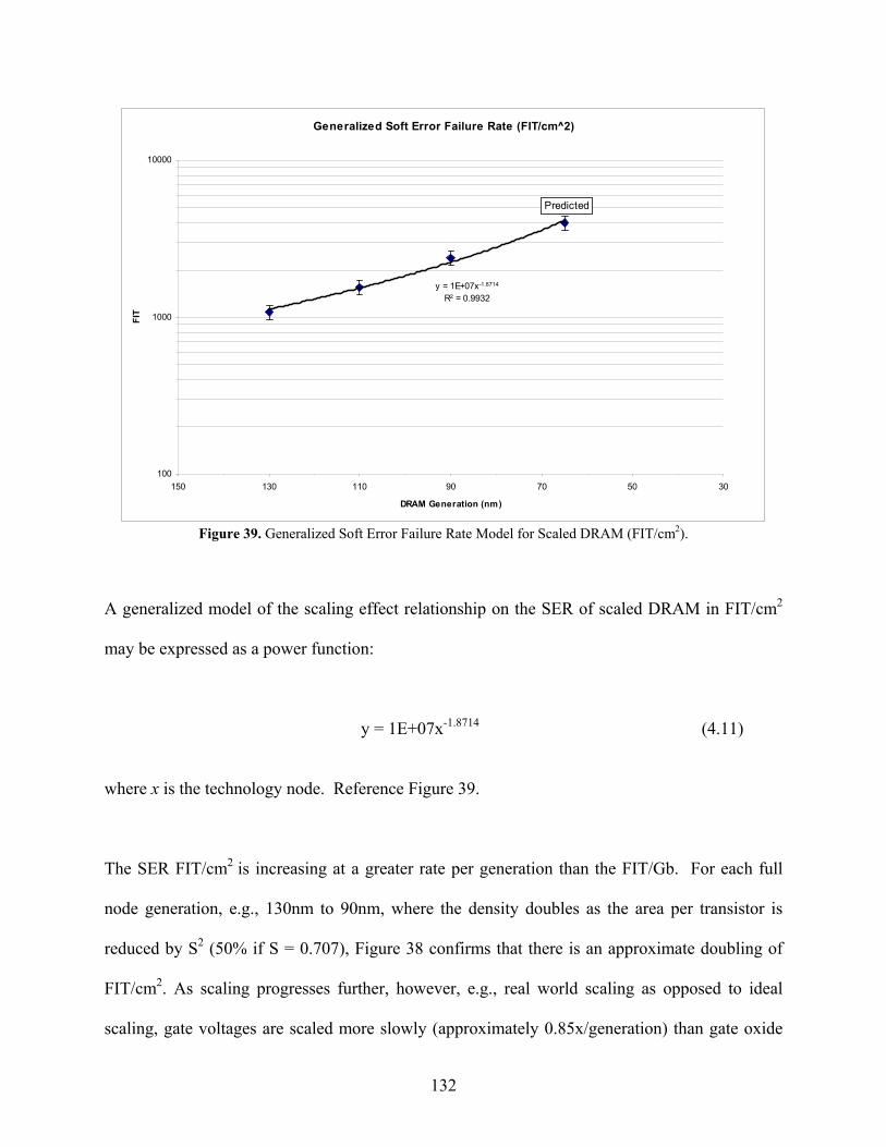
132
Figure 39. Generalized Soft Error Failure Rate Model for Scaled DRAM (FIT/cm2).
A generalized model of the scaling effect relationship on the SER of scaled DRAM in FIT/cm2
may be expressed as a power function:
y = 1E+07x-1.8714 (4.11)
where x is the technology node. Reference Figure 39.
The SER FIT/cm2 is increasing at a greater rate per generation than the FIT/Gb. For each full
node generation, e.g., 130nm to 90nm, where the density doubles as the area per transistor is
reduced by S2 (50% if S = 0.707), Figure 38 confirms that there is an approximate doubling of
FIT/cm2. As scaling progresses further, however, e.g., real world scaling as opposed to ideal
scaling, gate voltages are scaled more slowly (approximately 0.85x/generation) than gate oxide
Generalized Soft Error Failure Rate (FIT/cm^2)
y = 1E+07x-1.8714
R2 = 0.9932
100
1000
10000
30507090110130150
DRAM Generation (nm)
FIT
Predicted
133
thickness in order to maintain transistor saturation currents and signal speed. In general, the
ITRS roadmap shows the density progression for each successive technology and should be
considered in future generation projections.
The reliability (FIT/Gb) and quality (DD) of the DRAM parts with respect to retention time
characteristics is improving with each technology generation under equivalent stress conditions.
The observed difference in soft error failure rate, however, is more pronounced at higher stress
conditions. The normalized SER (FIT/cm2) is increasing with each progressive generation,
therefore. the SER FIT for the product, or system has to take this into account, e.g. the density
factor in Eq. 5.10. The user should consider these trends in the selection of a scaled DRAM
product for a given application and the anticipated operating conditions. Increases in operating
frequency, power dissipation, and junction temperature will each have a detrimental effect in
determining the product reliability for a given application. The user must also consider the
impact of SER on the increasing product density with each newer generation.
134
Chapter 5: Conclusion
5.1 Background
A description of the historical and modern approaches in assessing and predicting
microelectronics reliability, including the motivation for further investigation into this important
field of study, particularly for high reliability applications such as NASA spacecraft avionics is
provided. A synopsis of microelectronics derating and reliability modeling and simulation is
presented. CMOS technology scaling has an impact on circuit performance, power, circuit
design, burn-in and long term reliability in modern day microelectronics; these effects and trends
on microelectronics reliability are discussed. In addition, the Physics-of-Failure methodology,
competing mechanism theory, common intrinsic failure mechanisms and statistical models, and
the multiple failure mechanism model, are discussed and different approaches to calculate
acceleration factors are summarized.
5.2 Conclusion
A design of experiments and an accelerated stress test on scaled commercial SDRAMs was
performed. The goal of the SDRAM experiment was to investigate failure mechanism induced
degradation at the product level, and determine if long term performance is random (constant
rate process) or degrades over time (increasing failure rate). Additionally, characterization of
product sensitivities to temperature and voltage at the product level across different scaled
technologies was conducted.
135
Technology and construction analysis, device characterization, and data analysis led to a
degradation and predictive model, reliability assessment and defect density calculations of three
current SDRAM technologies for different stress conditions. Product, or system level soft error
rates for data retention were calculated, and an AF test matrix with the acceleration factors for
different combinations of temperature and voltage stresses is proposed. A methodology to
determine the density of random defects per cm2 of DRAM memory, and a forecast for the next
technology generation of scaled DRAM is included. This technique may be applied to other
scaled microelectronic devices and key parameters.
Retention time margin of several product generations is measured using a Q-ratio of the time-to-
first-failure distribution (t1) to the maximum specified refresh time, (tM). This ratio provides
insight into the tolerance of each technology generation to degradation with respect to voltage
and temperature stresses. The ratio also provides a quality factor demonstrating the amount of
margin between actual soft breakdown of a memory cell, and the manufacturer’s specified
refresh time.
A direct comparison of the data retention characteristics across three DRAM product
technologies reveals that a recoverable soft error breakdown occurs with each memory cell, and
that memory retention time gradually degrades over time. Two distinct populations are evident
with data retention breakdown; the main population soft error rate of each product generation
follows a Weibull distribution with a β slope > 2.4, while early failures are randomly distributed
with a β slope ~ 1.0. Data retention breakdown is accelerated by both temperature and voltage
stresses as is shown in Chapter 4. The study shows that up to 0.58% of the 130nm memory cells
136
in the scaled DRAM products studied are statistically random defective bits, and that the
percentage of random defective bits decreases to 0.32% for the 90nm memory cells. A prediction
is made for the number of random defective bits for the 65nm technology node given the ever
tighter process controls needed for nanometer scaled semiconductors and memory products. By
incorporating the defect rates for each representative technology with the cell characteristics, the
defect density per cm2 of DRAM memory ranges from 3.19x106 bits/cm2 for the 130nm product
technology, to 4.768x106 bits/cm2 for the 90nm product technology. A defect density prediction
is made for the next generation 65nm technology node.
Early soft errors and acceleration factors from each of the different temperature and voltage
conditions were analyzed against existing competing and multiple mechanism physical failure
models. The multiple failure mechanism AF model using the Power Law for AFv best fits the
DRAM retention time data and suggests a single temperature and voltage activated breakdown
mechanism.
Data was normalized to FIT/Gb and FIT/cm2 for the soft error rates to compare technology
generations, and a generalized model of the scaling effect relationship was developed. It was
shown that the reliability in FIT/Gb and quality (defect density) of the DRAM parts with respect
to retention time characteristics is improving with each technology generation under equivalent
stress conditions. The observed difference in soft error failure rate, however, is more
pronounced at higher stress conditions. The normalized SER (FIT/cm2) is increasing with each
progressive generation, therefore, the SER FIT for the product, or system must be considered.
The user must balance this knowledge with the anticipated application operating conditions.
137
Increases in operating frequency, power dissipation, and junction temperature will each have a
detrimental effect in determining the product reliability for a given application.
The data and the derived acceleration and derating factors demonstrate that a combination of
temperature and voltage stresses are better for screening out and/or qualification of scaled
DRAM products for defects that may lead to premature failure in the application.
A summary of the nonlinear regression analysis for the SDRAM study is included in Appendix
A.
The DRAM experimental results are particularly important for several reasons:
1) For the same density memory chip and equivalent stress conditions, the product or system
reliability should increase for each successive technology generation as manufacturers
strive to maintain product FIT rates for higher density memories. The DRAM results
support this trend.
2) NASA and the aerospace industry have historically used temperature only as a stress
driver to screen and qualify parts. This data supports that a combination of temperature
and voltage stresses better accelerates both thermally and voltage driven mechanisms that
could impact long term parts reliability. This method also better identifies the weak
memory cells that lead to early breakdown.
138
3) A temperature and voltage stress test matrix approach shows the expected acceleration
factor or derating factor for different temperature and voltage stress combinations on the
data retention soft error rate for 130nm, 110nm and 90nm SDRAM product technologies.
A similar screening and/or qualification approach may be adapted for other parts and
newer product generations. The user should use caution and test the specific product
family, technology, and manufacturer to determine accurate acceleration and derating
factors at different stress combinations, especially for critical applications. Differences in
over-voltage protection schemes, device layout, design, and other factors can impact the
level of voltage stress actually applied deep inside the core of the chip circuitry. In many
cases, discrete level testing is desirable and preferred to determine accurate voltage
acceleration factors for the core circuitry, as these may be different than those observed at
the product level.
4) Results show that early failures are dominated by CFR, Beta = 1, for each technology in
the study.
5) Results show that the reliability is improving and failure rate (FIT/Gb) is decreasing with
each new technology under equivalent stress conditions.
6) Results show that for the same size memory, e.g. 512Mb, the quality (defect density) is
improving with each new technology generation. Therefore, the 90nm products exhibit
better retention time characteristics and fewer defects/cm2 than the larger 110nm and
130nm technologies.
139
7) Results show that the normalized soft error rate (FIT/cm2) is increasing with each new
technology generations.
5.3 Future Work
Ongoing research, accelerated stress testing, and modeling of scaling effects on microelectronics
reliability continues throughout the industry. Newer product technologies, including 65nm,
45nm, and 32nm need to be studied to determine if developments in materials, design, layout,
and processing will inherently affect the reliability of next generation microelectronics. The
evaluation methodology described herein, however, may be applied to other product
technologies.
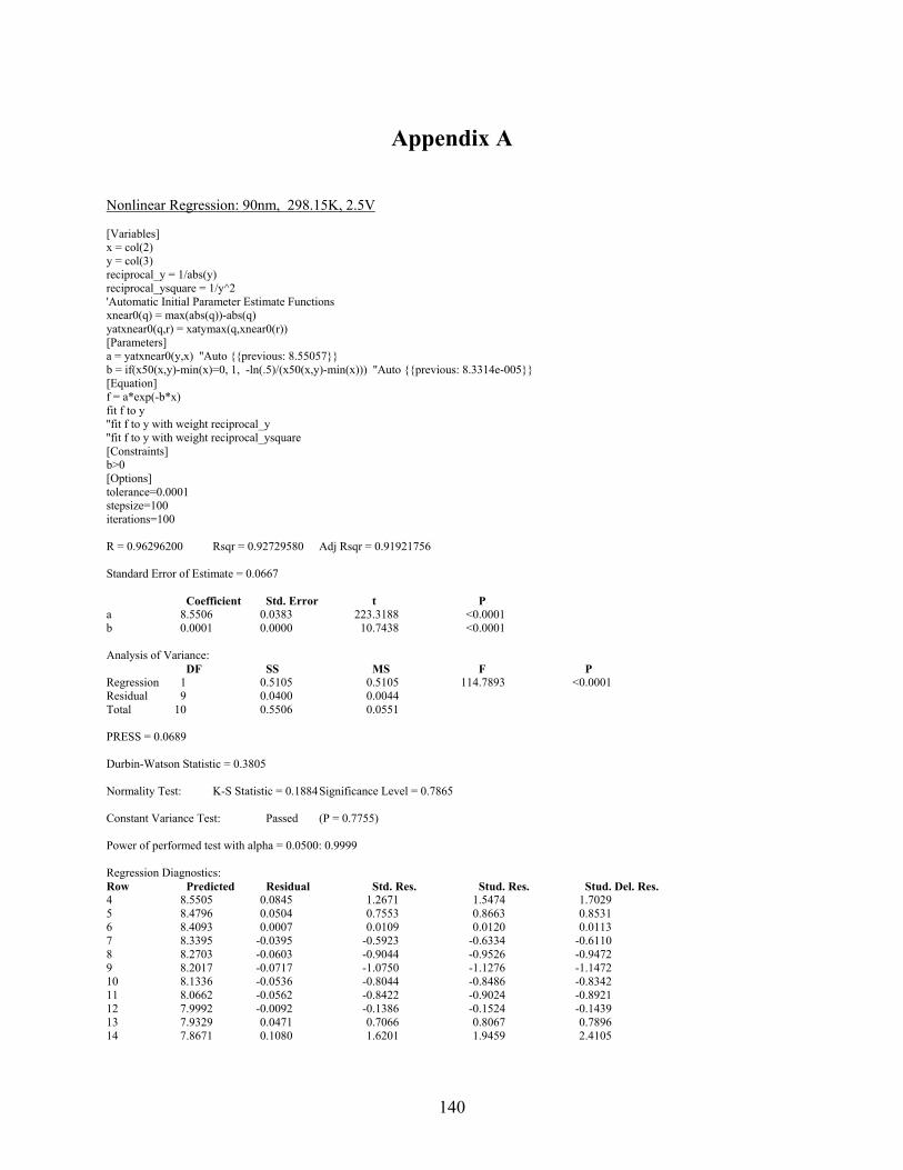
140
Appendix A
Nonlinear Regression: 90nm, 298.15K, 2.5V [Variables] x = col(2) y = col(3) reciprocal_y = 1/abs(y) reciprocal_ysquare = 1/y^2 'Automatic Initial Parameter Estimate Functions xnear0(q) = max(abs(q))-abs(q) yatxnear0(q,r) = xatymax(q,xnear0(r)) [Parameters] a = yatxnear0(y,x) ''Auto previous: 8.55057 b = if(x50(x,y)-min(x)=0, 1, -ln(.5)/(x50(x,y)-min(x))) ''Auto previous: 8.3314e-005 [Equation] f = a*exp(-b*x) fit f to y ''fit f to y with weight reciprocal_y ''fit f to y with weight reciprocal_ysquare [Constraints] b>0 [Options] tolerance=0.0001 stepsize=100 iterations=100 R = 0.96296200 Rsqr = 0.92729580 Adj Rsqr = 0.91921756 Standard Error of Estimate = 0.0667 Coefficient Std. Error t P a 8.5506 0.0383 223.3188 <0.0001 b 0.0001 0.0000 10.7438 <0.0001 Analysis of Variance: DF SS MS F P Regression 1 0.5105 0.5105 114.7893 <0.0001 Residual 9 0.0400 0.0044 Total 10 0.5506 0.0551 PRESS = 0.0689 Durbin-Watson Statistic = 0.3805 Normality Test: K-S Statistic = 0.1884 Significance Level = 0.7865 Constant Variance Test: Passed (P = 0.7755) Power of performed test with alpha = 0.0500: 0.9999 Regression Diagnostics: Row Predicted Residual Std. Res. Stud. Res. Stud. Del. Res. 4 8.5505 0.0845 1.2671 1.5474 1.7029 5 8.4796 0.0504 0.7553 0.8663 0.8531 6 8.4093 0.0007 0.0109 0.0120 0.0113 7 8.3395 -0.0395 -0.5923 -0.6334 -0.6110 8 8.2703 -0.0603 -0.9044 -0.9526 -0.9472 9 8.2017 -0.0717 -1.0750 -1.1276 -1.1472 10 8.1336 -0.0536 -0.8044 -0.8486 -0.8342 11 8.0662 -0.0562 -0.8422 -0.9024 -0.8921 12 7.9992 -0.0092 -0.1386 -0.1524 -0.1439 13 7.9329 0.0471 0.7066 0.8067 0.7896 14 7.8671 0.1080 1.6201 1.9459 2.4105
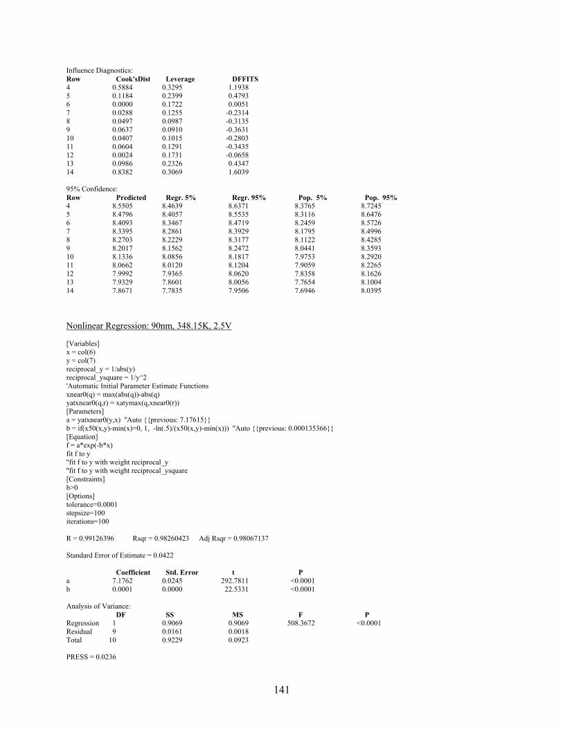
141
Influence Diagnostics: Row Cook'sDist Leverage DFFITS 4 0.5884 0.3295 1.1938 5 0.1184 0.2399 0.4793 6 0.0000 0.1722 0.0051 7 0.0288 0.1255 -0.2314 8 0.0497 0.0987 -0.3135 9 0.0637 0.0910 -0.3631 10 0.0407 0.1015 -0.2803 11 0.0604 0.1291 -0.3435 12 0.0024 0.1731 -0.0658 13 0.0986 0.2326 0.4347 14 0.8382 0.3069 1.6039 95% Confidence: Row Predicted Regr. 5% Regr. 95% Pop. 5% Pop. 95% 4 8.5505 8.4639 8.6371 8.3765 8.7245 5 8.4796 8.4057 8.5535 8.3116 8.6476 6 8.4093 8.3467 8.4719 8.2459 8.5726 7 8.3395 8.2861 8.3929 8.1795 8.4996 8 8.2703 8.2229 8.3177 8.1122 8.4285 9 8.2017 8.1562 8.2472 8.0441 8.3593 10 8.1336 8.0856 8.1817 7.9753 8.2920 11 8.0662 8.0120 8.1204 7.9059 8.2265 12 7.9992 7.9365 8.0620 7.8358 8.1626 13 7.9329 7.8601 8.0056 7.7654 8.1004 14 7.8671 7.7835 7.9506 7.6946 8.0395
Nonlinear Regression: 90nm, 348.15K, 2.5V [Variables] x = col(6) y = col(7) reciprocal_y = 1/abs(y) reciprocal_ysquare = 1/y^2 'Automatic Initial Parameter Estimate Functions xnear0(q) = max(abs(q))-abs(q) yatxnear0(q,r) = xatymax(q,xnear0(r)) [Parameters] a = yatxnear0(y,x) ''Auto previous: 7.17615 b = if(x50(x,y)-min(x)=0, 1, -ln(.5)/(x50(x,y)-min(x))) ''Auto previous: 0.000135366 [Equation] f = a*exp(-b*x) fit f to y ''fit f to y with weight reciprocal_y ''fit f to y with weight reciprocal_ysquare [Constraints] b>0 [Options] tolerance=0.0001 stepsize=100 iterations=100 R = 0.99126396 Rsqr = 0.98260423 Adj Rsqr = 0.98067137 Standard Error of Estimate = 0.0422 Coefficient Std. Error t P a 7.1762 0.0245 292.7811 <0.0001 b 0.0001 0.0000 22.5331 <0.0001 Analysis of Variance: DF SS MS F P Regression 1 0.9069 0.9069 508.3672 <0.0001 Residual 9 0.0161 0.0018 Total 10 0.9229 0.0923 PRESS = 0.0236
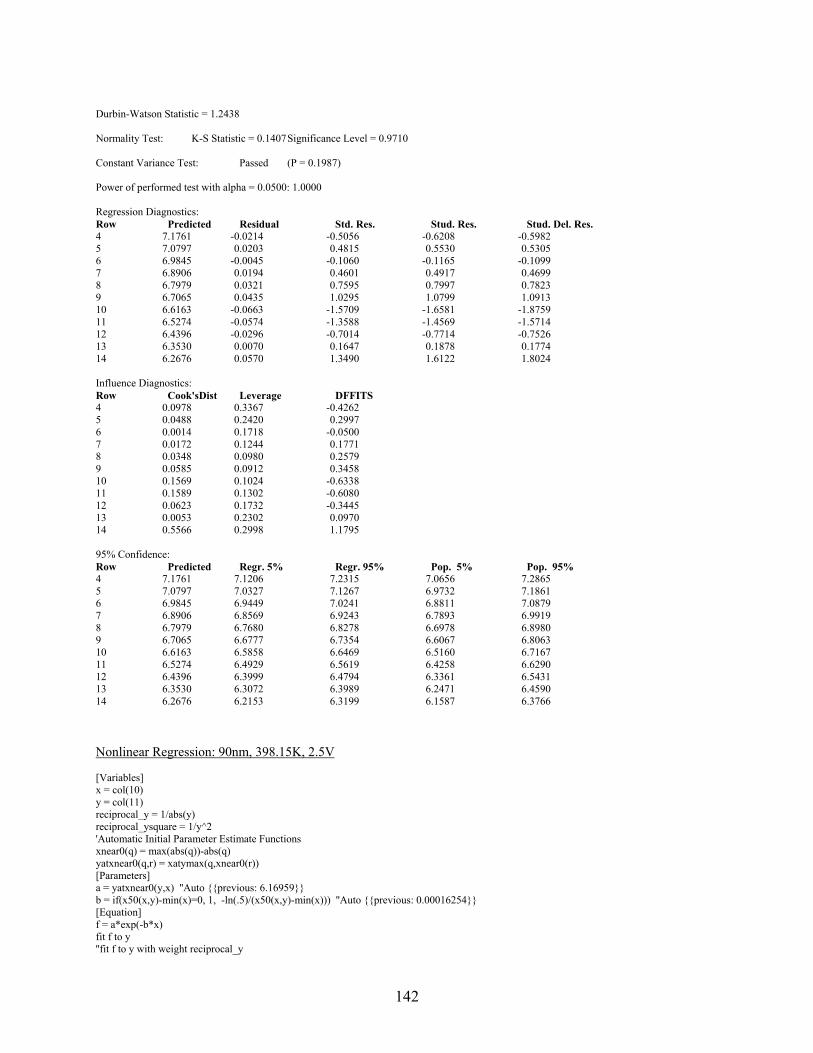
142
Durbin-Watson Statistic = 1.2438 Normality Test: K-S Statistic = 0.1407 Significance Level = 0.9710 Constant Variance Test: Passed (P = 0.1987) Power of performed test with alpha = 0.0500: 1.0000 Regression Diagnostics: Row Predicted Residual Std. Res. Stud. Res. Stud. Del. Res. 4 7.1761 -0.0214 -0.5056 -0.6208 -0.5982 5 7.0797 0.0203 0.4815 0.5530 0.5305 6 6.9845 -0.0045 -0.1060 -0.1165 -0.1099 7 6.8906 0.0194 0.4601 0.4917 0.4699 8 6.7979 0.0321 0.7595 0.7997 0.7823 9 6.7065 0.0435 1.0295 1.0799 1.0913 10 6.6163 -0.0663 -1.5709 -1.6581 -1.8759 11 6.5274 -0.0574 -1.3588 -1.4569 -1.5714 12 6.4396 -0.0296 -0.7014 -0.7714 -0.7526 13 6.3530 0.0070 0.1647 0.1878 0.1774 14 6.2676 0.0570 1.3490 1.6122 1.8024 Influence Diagnostics: Row Cook'sDist Leverage DFFITS 4 0.0978 0.3367 -0.4262 5 0.0488 0.2420 0.2997 6 0.0014 0.1718 -0.0500 7 0.0172 0.1244 0.1771 8 0.0348 0.0980 0.2579 9 0.0585 0.0912 0.3458 10 0.1569 0.1024 -0.6338 11 0.1589 0.1302 -0.6080 12 0.0623 0.1732 -0.3445 13 0.0053 0.2302 0.0970 14 0.5566 0.2998 1.1795 95% Confidence: Row Predicted Regr. 5% Regr. 95% Pop. 5% Pop. 95% 4 7.1761 7.1206 7.2315 7.0656 7.2865 5 7.0797 7.0327 7.1267 6.9732 7.1861 6 6.9845 6.9449 7.0241 6.8811 7.0879 7 6.8906 6.8569 6.9243 6.7893 6.9919 8 6.7979 6.7680 6.8278 6.6978 6.8980 9 6.7065 6.6777 6.7354 6.6067 6.8063 10 6.6163 6.5858 6.6469 6.5160 6.7167 11 6.5274 6.4929 6.5619 6.4258 6.6290 12 6.4396 6.3999 6.4794 6.3361 6.5431 13 6.3530 6.3072 6.3989 6.2471 6.4590 14 6.2676 6.2153 6.3199 6.1587 6.3766
Nonlinear Regression: 90nm, 398.15K, 2.5V [Variables] x = col(10) y = col(11) reciprocal_y = 1/abs(y) reciprocal_ysquare = 1/y^2 'Automatic Initial Parameter Estimate Functions xnear0(q) = max(abs(q))-abs(q) yatxnear0(q,r) = xatymax(q,xnear0(r)) [Parameters] a = yatxnear0(y,x) ''Auto previous: 6.16959 b = if(x50(x,y)-min(x)=0, 1, -ln(.5)/(x50(x,y)-min(x))) ''Auto previous: 0.00016254 [Equation] f = a*exp(-b*x) fit f to y ''fit f to y with weight reciprocal_y
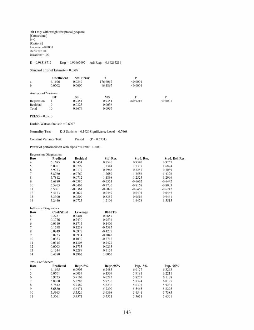
143
''fit f to y with weight reciprocal_ysquare [Constraints] b>0 [Options] tolerance=0.0001 stepsize=100 iterations=100 R = 0.98318715 Rsqr = 0.96665697 Adj Rsqr = 0.96295219 Standard Error of Estimate = 0.0599 Coefficient Std. Error t P a 6.1696 0.0349 176.6067 <0.0001 b 0.0002 0.0000 16.1867 <0.0001 Analysis of Variance: DF SS MS F P Regression 1 0.9351 0.9351 260.9215 <0.0001 Residual 9 0.0323 0.0036 Total 10 0.9674 0.0967 PRESS = 0.0510 Durbin-Watson Statistic = 0.6007 Normality Test: K-S Statistic = 0.1920 Significance Level = 0.7668 Constant Variance Test: Passed (P = 0.6731) Power of performed test with alpha = 0.0500: 1.0000 Regression Diagnostics: Row Predicted Residual Std. Res. Stud. Res. Stud. Del. Res. 4 6.1695 0.0454 0.7586 0.9340 0.9267 5 6.0701 0.0799 1.3344 1.5337 1.6824 6 5.9723 0.0177 0.2965 0.3257 0.3089 7 5.8760 -0.0760 -1.2689 -1.3556 -1.4326 8 5.7812 -0.0712 -1.1898 -1.2525 -1.2996 9 5.6880 -0.0380 -0.6351 -0.6662 -0.6442 10 5.5963 -0.0463 -0.7736 -0.8168 -0.8003 11 5.5061 -0.0361 -0.6028 -0.6465 -0.6242 12 5.4173 0.0027 0.0449 0.0494 0.0465 13 5.3300 0.0500 0.8357 0.9516 0.9461 14 5.2440 0.0725 1.2104 1.4428 1.5515 Influence Diagnostics: Row Cook'sDist Leverage DFFITS 4 0.2251 0.3404 0.6657 5 0.3776 0.2430 0.9534 6 0.0110 0.1715 0.1406 7 0.1298 0.1238 -0.5385 8 0.0849 0.0977 -0.4277 9 0.0223 0.0914 -0.2043 10 0.0383 0.1030 -0.2712 11 0.0315 0.1308 -0.2422 12 0.0003 0.1733 0.0213 13 0.1344 0.2289 0.5154 14 0.4380 0.2962 1.0065 95% Confidence: Row Predicted Regr. 5% Regr. 95% Pop. 5% Pop. 95% 4 6.1695 6.0905 6.2485 6.0127 6.3263 5 6.0701 6.0034 6.1369 5.9191 6.2211 6 5.9723 5.9162 6.0283 5.8257 6.1188 7 5.8760 5.8283 5.9236 5.7324 6.0195 8 5.7812 5.7389 5.8236 5.6393 5.9231 9 5.6880 5.6471 5.7290 5.5465 5.8295 10 5.5963 5.5529 5.6398 5.4541 5.7385 11 5.5061 5.4571 5.5551 5.3621 5.6501
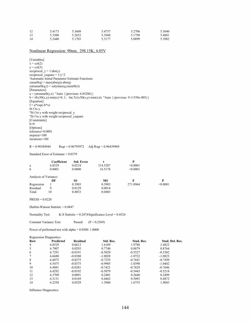
144
12 5.4173 5.3609 5.4737 5.2706 5.5640 13 5.3300 5.2652 5.3948 5.1798 5.4801 14 5.2440 5.1703 5.3177 5.0899 5.3982
Nonlinear Regression: 90nm, 298.15K, 4.05V [Variables] x = col(2) y = col(3) reciprocal_y = 1/abs(y) reciprocal_ysquare = 1/y^2 'Automatic Initial Parameter Estimate Functions xnear0(q) = max(abs(q))-abs(q) yatxnear0(q,r) = xatymax(q,xnear0(r)) [Parameters] a = yatxnear0(y,x) ''Auto previous: 6.85286 b = if(x50(x,y)-min(x)=0, 1, -ln(.5)/(x50(x,y)-min(x))) ''Auto previous: 9.11558e-005 [Equation] f = a*exp(-b*x) fit f to y ''fit f to y with weight reciprocal_y ''fit f to y with weight reciprocal_ysquare [Constraints] b>0 [Options] tolerance=0.0001 stepsize=100 iterations=100 R = 0.98384944 Rsqr = 0.96795972 Adj Rsqr = 0.96439969 Standard Error of Estimate = 0.0379 Coefficient Std. Error t P a 6.8529 0.0218 314.5287 <0.0001 b 0.0001 0.0000 16.5178 <0.0001 Analysis of Variance: DF SS MS F P Regression 1 0.3903 0.3903 271.8964 <0.0001 Residual 9 0.0129 0.0014 Total 10 0.4033 0.0403 PRESS = 0.0228 Durbin-Watson Statistic = 0.4847 Normality Test: K-S Statistic = 0.2474 Significance Level = 0.4524 Constant Variance Test: Passed (P = 0.2569) Power of performed test with alpha = 0.0500: 1.0000 Regression Diagnostics: Row Predicted Residual Std. Res. Stud. Res. Stud. Del. Res. 4 6.8529 0.0613 1.6189 1.9788 2.4822 5 6.7907 0.0293 0.7740 0.8879 0.8764 6 6.7291 -0.0191 -0.5029 -0.5527 -0.5302 7 6.6680 -0.0380 -1.0028 -1.0722 -1.0823 8 6.6075 -0.0275 -0.7255 -0.7641 -0.7450 9 6.5475 -0.0375 -0.9905 -1.0390 -1.0442 10 6.4881 -0.0281 -0.7421 -0.7829 -0.7646 11 6.4292 -0.0192 -0.5079 -0.5443 -0.5218 12 6.3709 0.0091 0.2401 0.2640 0.2499 13 6.3131 0.0169 0.4462 0.5093 0.4872 14 6.2558 0.0529 1.3960 1.6755 1.9043 Influence Diagnostics:
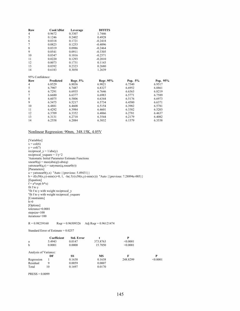
145
Row Cook'sDist Leverage DFFITS 4 0.9672 0.3307 1.7446 5 0.1246 0.2402 0.4928 6 0.0318 0.1721 -0.2418 7 0.0823 0.1253 -0.4096 8 0.0319 0.0986 -0.2464 9 0.0541 0.0911 -0.3305 10 0.0347 0.1016 -0.2571 11 0.0220 0.1293 -0.2010 12 0.0073 0.1731 0.1143 13 0.0392 0.2323 0.2680 14 0.6183 0.3058 1.2639 95% Confidence: Row Predicted Regr. 5% Regr. 95% Pop. 5% Pop. 95% 4 6.8529 6.8036 6.9021 6.7540 6.9517 5 6.7907 6.7487 6.8327 6.6952 6.8861 6 6.7291 6.6935 6.7646 6.6363 6.8219 7 6.6680 6.6377 6.6983 6.5771 6.7589 8 6.6075 6.5806 6.6344 6.5176 6.6973 9 6.5475 6.5217 6.5734 6.4580 6.6371 10 6.4881 6.4608 6.5154 6.3982 6.5781 11 6.4292 6.3984 6.4601 6.3382 6.5203 12 6.3709 6.3352 6.4066 6.2781 6.4637 13 6.3131 6.2718 6.3544 6.2179 6.4082 14 6.2558 6.2084 6.3032 6.1579 6.3538
Nonlinear Regression: 90nm, 348.15K, 4.05V [Variables] x = col(6) y = col(7) reciprocal_y = 1/abs(y) reciprocal_ysquare = 1/y^2 'Automatic Initial Parameter Estimate Functions xnear0(q) = max(abs(q))-abs(q) yatxnear0(q,r) = xatymax(q,xnear0(r)) [Parameters] a = yatxnear0(y,x) ''Auto previous: 5.49431 b = if(x50(x,y)-min(x)=0, 1, -ln(.5)/(x50(x,y)-min(x))) ''Auto previous: 7.28894e-005 [Equation] f = a*exp(-b*x) fit f to y ''fit f to y with weight reciprocal_y ''fit f to y with weight reciprocal_ysquare [Constraints] b>0 [Options] tolerance=0.0001 stepsize=100 iterations=100 R = 0.98239160 Rsqr = 0.96509326 Adj Rsqr = 0.96121474 Standard Error of Estimate = 0.0257 Coefficient Std. Error t P a 5.4943 0.0147 373.8763 <0.0001 b 0.0001 0.0000 15.7850 <0.0001 Analysis of Variance: DF SS MS F P Regression 1 0.1638 0.1638 248.8299 <0.0001 Residual 9 0.0059 0.0007 Total 10 0.1697 0.0170 PRESS = 0.0099
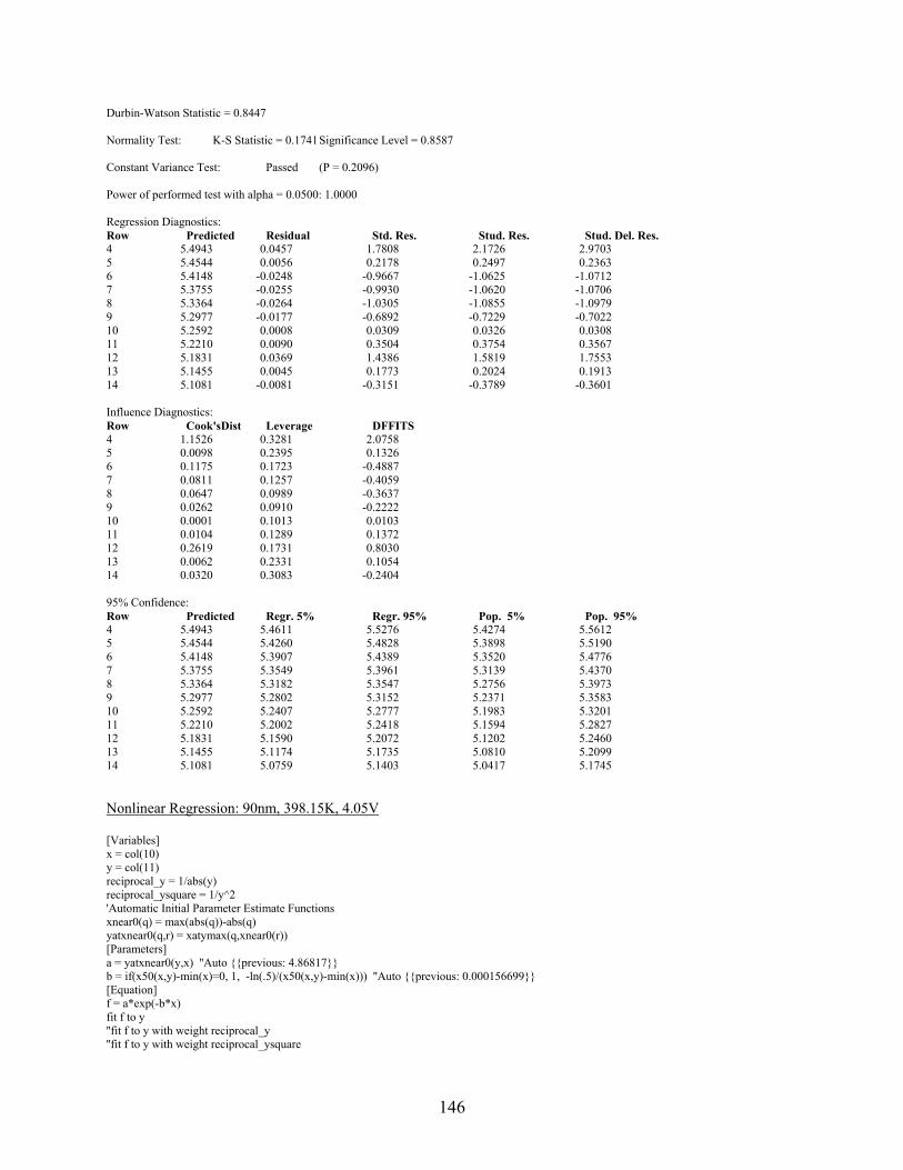
146
Durbin-Watson Statistic = 0.8447 Normality Test: K-S Statistic = 0.1741 Significance Level = 0.8587 Constant Variance Test: Passed (P = 0.2096) Power of performed test with alpha = 0.0500: 1.0000 Regression Diagnostics: Row Predicted Residual Std. Res. Stud. Res. Stud. Del. Res. 4 5.4943 0.0457 1.7808 2.1726 2.9703 5 5.4544 0.0056 0.2178 0.2497 0.2363 6 5.4148 -0.0248 -0.9667 -1.0625 -1.0712 7 5.3755 -0.0255 -0.9930 -1.0620 -1.0706 8 5.3364 -0.0264 -1.0305 -1.0855 -1.0979 9 5.2977 -0.0177 -0.6892 -0.7229 -0.7022 10 5.2592 0.0008 0.0309 0.0326 0.0308 11 5.2210 0.0090 0.3504 0.3754 0.3567 12 5.1831 0.0369 1.4386 1.5819 1.7553 13 5.1455 0.0045 0.1773 0.2024 0.1913 14 5.1081 -0.0081 -0.3151 -0.3789 -0.3601 Influence Diagnostics: Row Cook'sDist Leverage DFFITS 4 1.1526 0.3281 2.0758 5 0.0098 0.2395 0.1326 6 0.1175 0.1723 -0.4887 7 0.0811 0.1257 -0.4059 8 0.0647 0.0989 -0.3637 9 0.0262 0.0910 -0.2222 10 0.0001 0.1013 0.0103 11 0.0104 0.1289 0.1372 12 0.2619 0.1731 0.8030 13 0.0062 0.2331 0.1054 14 0.0320 0.3083 -0.2404 95% Confidence: Row Predicted Regr. 5% Regr. 95% Pop. 5% Pop. 95% 4 5.4943 5.4611 5.5276 5.4274 5.5612 5 5.4544 5.4260 5.4828 5.3898 5.5190 6 5.4148 5.3907 5.4389 5.3520 5.4776 7 5.3755 5.3549 5.3961 5.3139 5.4370 8 5.3364 5.3182 5.3547 5.2756 5.3973 9 5.2977 5.2802 5.3152 5.2371 5.3583 10 5.2592 5.2407 5.2777 5.1983 5.3201 11 5.2210 5.2002 5.2418 5.1594 5.2827 12 5.1831 5.1590 5.2072 5.1202 5.2460 13 5.1455 5.1174 5.1735 5.0810 5.2099 14 5.1081 5.0759 5.1403 5.0417 5.1745
Nonlinear Regression: 90nm, 398.15K, 4.05V [Variables] x = col(10) y = col(11) reciprocal_y = 1/abs(y) reciprocal_ysquare = 1/y^2 'Automatic Initial Parameter Estimate Functions xnear0(q) = max(abs(q))-abs(q) yatxnear0(q,r) = xatymax(q,xnear0(r)) [Parameters] a = yatxnear0(y,x) ''Auto previous: 4.86817 b = if(x50(x,y)-min(x)=0, 1, -ln(.5)/(x50(x,y)-min(x))) ''Auto previous: 0.000156699 [Equation] f = a*exp(-b*x) fit f to y ''fit f to y with weight reciprocal_y ''fit f to y with weight reciprocal_ysquare
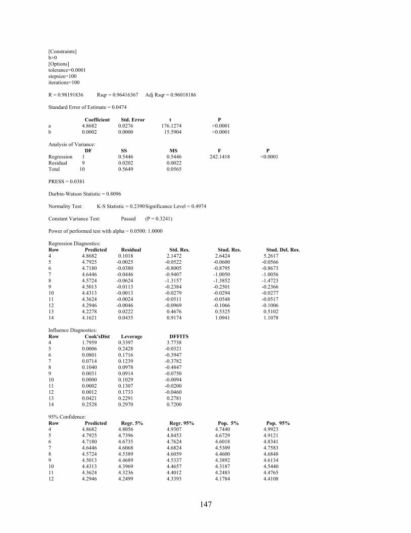
147
[Constraints] b>0 [Options] tolerance=0.0001 stepsize=100 iterations=100 R = 0.98191836 Rsqr = 0.96416367 Adj Rsqr = 0.96018186 Standard Error of Estimate = 0.0474 Coefficient Std. Error t P a 4.8682 0.0276 176.1274 <0.0001 b 0.0002 0.0000 15.5904 <0.0001 Analysis of Variance: DF SS MS F P Regression 1 0.5446 0.5446 242.1418 <0.0001 Residual 9 0.0202 0.0022 Total 10 0.5649 0.0565 PRESS = 0.0381 Durbin-Watson Statistic = 0.8096 Normality Test: K-S Statistic = 0.2390 Significance Level = 0.4974 Constant Variance Test: Passed (P = 0.3241) Power of performed test with alpha = 0.0500: 1.0000 Regression Diagnostics: Row Predicted Residual Std. Res. Stud. Res. Stud. Del. Res. 4 4.8682 0.1018 2.1472 2.6424 5.2617 5 4.7925 -0.0025 -0.0522 -0.0600 -0.0566 6 4.7180 -0.0380 -0.8005 -0.8795 -0.8673 7 4.6446 -0.0446 -0.9407 -1.0050 -1.0056 8 4.5724 -0.0624 -1.3157 -1.3852 -1.4723 9 4.5013 -0.0113 -0.2384 -0.2501 -0.2366 10 4.4313 -0.0013 -0.0279 -0.0294 -0.0277 11 4.3624 -0.0024 -0.0511 -0.0548 -0.0517 12 4.2946 -0.0046 -0.0969 -0.1066 -0.1006 13 4.2278 0.0222 0.4676 0.5325 0.5102 14 4.1621 0.0435 0.9174 1.0941 1.1078 Influence Diagnostics: Row Cook'sDist Leverage DFFITS 4 1.7959 0.3397 3.7738 5 0.0006 0.2428 -0.0321 6 0.0801 0.1716 -0.3947 7 0.0714 0.1239 -0.3782 8 0.1040 0.0978 -0.4847 9 0.0031 0.0914 -0.0750 10 0.0000 0.1029 -0.0094 11 0.0002 0.1307 -0.0200 12 0.0012 0.1733 -0.0460 13 0.0421 0.2291 0.2781 14 0.2528 0.2970 0.7200 95% Confidence: Row Predicted Regr. 5% Regr. 95% Pop. 5% Pop. 95% 4 4.8682 4.8056 4.9307 4.7440 4.9923 5 4.7925 4.7396 4.8453 4.6729 4.9121 6 4.7180 4.6735 4.7624 4.6018 4.8341 7 4.6446 4.6068 4.6824 4.5309 4.7583 8 4.5724 4.5389 4.6059 4.4600 4.6848 9 4.5013 4.4689 4.5337 4.3892 4.6134 10 4.4313 4.3969 4.4657 4.3187 4.5440 11 4.3624 4.3236 4.4012 4.2483 4.4765 12 4.2946 4.2499 4.3393 4.1784 4.4108
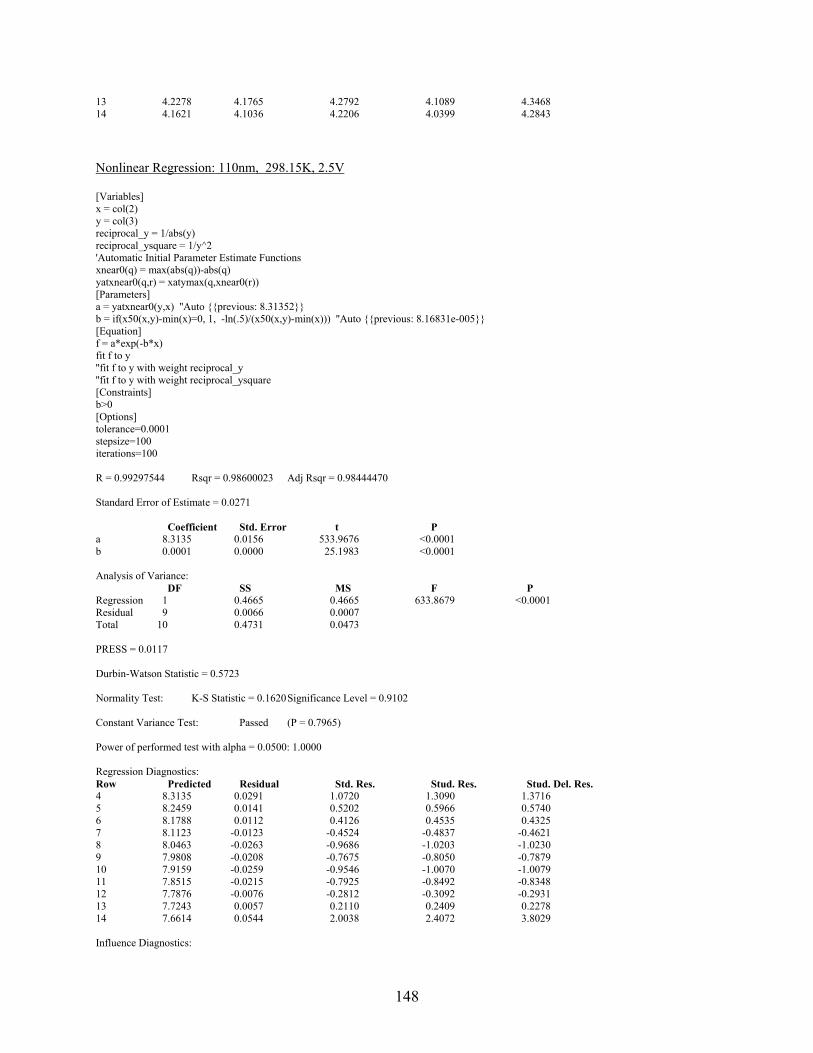
148
13 4.2278 4.1765 4.2792 4.1089 4.3468 14 4.1621 4.1036 4.2206 4.0399 4.2843
Nonlinear Regression: 110nm, 298.15K, 2.5V [Variables] x = col(2) y = col(3) reciprocal_y = 1/abs(y) reciprocal_ysquare = 1/y^2 'Automatic Initial Parameter Estimate Functions xnear0(q) = max(abs(q))-abs(q) yatxnear0(q,r) = xatymax(q,xnear0(r)) [Parameters] a = yatxnear0(y,x) ''Auto previous: 8.31352 b = if(x50(x,y)-min(x)=0, 1, -ln(.5)/(x50(x,y)-min(x))) ''Auto previous: 8.16831e-005 [Equation] f = a*exp(-b*x) fit f to y ''fit f to y with weight reciprocal_y ''fit f to y with weight reciprocal_ysquare [Constraints] b>0 [Options] tolerance=0.0001 stepsize=100 iterations=100 R = 0.99297544 Rsqr = 0.98600023 Adj Rsqr = 0.98444470 Standard Error of Estimate = 0.0271 Coefficient Std. Error t P a 8.3135 0.0156 533.9676 <0.0001 b 0.0001 0.0000 25.1983 <0.0001 Analysis of Variance: DF SS MS F P Regression 1 0.4665 0.4665 633.8679 <0.0001 Residual 9 0.0066 0.0007 Total 10 0.4731 0.0473 PRESS = 0.0117 Durbin-Watson Statistic = 0.5723 Normality Test: K-S Statistic = 0.1620 Significance Level = 0.9102 Constant Variance Test: Passed (P = 0.7965) Power of performed test with alpha = 0.0500: 1.0000 Regression Diagnostics: Row Predicted Residual Std. Res. Stud. Res. Stud. Del. Res. 4 8.3135 0.0291 1.0720 1.3090 1.3716 5 8.2459 0.0141 0.5202 0.5966 0.5740 6 8.1788 0.0112 0.4126 0.4535 0.4325 7 8.1123 -0.0123 -0.4524 -0.4837 -0.4621 8 8.0463 -0.0263 -0.9686 -1.0203 -1.0230 9 7.9808 -0.0208 -0.7675 -0.8050 -0.7879 10 7.9159 -0.0259 -0.9546 -1.0070 -1.0079 11 7.8515 -0.0215 -0.7925 -0.8492 -0.8348 12 7.7876 -0.0076 -0.2812 -0.3092 -0.2931 13 7.7243 0.0057 0.2110 0.2409 0.2278 14 7.6614 0.0544 2.0038 2.4072 3.8029 Influence Diagnostics:

149
Row Cook'sDist Leverage DFFITS 4 0.4207 0.3294 0.9612 5 0.0562 0.2398 0.3224 6 0.0214 0.1722 0.1973 7 0.0168 0.1255 -0.1751 8 0.0570 0.0988 -0.3386 9 0.0324 0.0910 -0.2493 10 0.0572 0.1014 -0.3386 11 0.0534 0.1291 -0.3214 12 0.0100 0.1731 -0.1341 13 0.0088 0.2327 0.1255 14 1.2840 0.3071 2.5316 95% Confidence: Row Predicted Regr. 5% Regr. 95% Pop. 5% Pop. 95% 4 8.3135 8.2783 8.3487 8.2428 8.3843 5 8.2459 8.2158 8.2759 8.1776 8.3142 6 8.1788 8.1533 8.2043 8.1124 8.2453 7 8.1123 8.0905 8.1340 8.0472 8.1774 8 8.0463 8.0270 8.0656 7.9819 8.1106 9 7.9808 7.9623 7.9993 7.9167 8.0449 10 7.9159 7.8964 7.9354 7.8515 7.9803 11 7.8515 7.8295 7.8735 7.7863 7.9167 12 7.7876 7.7621 7.8132 7.7212 7.8541 13 7.7243 7.6947 7.7539 7.6561 7.7924 14 7.6614 7.6274 7.6954 7.5913 7.7316 Nonlinear Regression: 110nm, 348.15K, 2.5V [Variables] x = col(6) y = col(7) reciprocal_y = 1/abs(y) reciprocal_ysquare = 1/y^2 'Automatic Initial Parameter Estimate Functions xnear0(q) = max(abs(q))-abs(q) yatxnear0(q,r) = xatymax(q,xnear0(r)) [Parameters] a = yatxnear0(y,x) ''Auto previous: 6.84254 b = if(x50(x,y)-min(x)=0, 1, -ln(.5)/(x50(x,y)-min(x))) ''Auto previous: 0.000120308 [Equation] f = a*exp(-b*x) fit f to y ''fit f to y with weight reciprocal_y ''fit f to y with weight reciprocal_ysquare [Constraints] b>0 [Options] tolerance=0.0001 stepsize=100 iterations=100 R = 0.95758184 Rsqr = 0.91696299 Adj Rsqr = 0.90773665 Standard Error of Estimate = 0.0812 Coefficient Std. Error t P a 6.8425 0.0470 145.6813 <0.0001 b 0.0001 0.0000 10.0099 <0.0001 Analysis of Variance: DF SS MS F P Regression 1 0.6552 0.6552 99.3854 <0.0001 Residual 9 0.0593 0.0066 Total 10 0.7145 0.0714 PRESS = 0.1004

150
Durbin-Watson Statistic = 0.3621 Normality Test: K-S Statistic = 0.1456 Significance Level = 0.9606 Constant Variance Test: Passed (P = 0.8601) Power of performed test with alpha = 0.0500: 0.9997 Regression Diagnostics: Row Predicted Residual Std. Res. Stud. Res. Stud. Del. Res. 4 6.8425 0.1219 1.5009 1.8400 2.1965 5 6.7607 0.0493 0.6070 0.6970 0.6756 6 6.6799 0.0001 0.0017 0.0018 0.0017 7 6.6000 -0.0600 -0.7388 -0.7896 -0.7717 8 6.5211 -0.1011 -1.2447 -1.3107 -1.3738 9 6.4431 -0.0831 -1.0232 -1.0733 -1.0836 10 6.3660 -0.0760 -0.9363 -0.9882 -0.9867 11 6.2899 -0.0299 -0.3682 -0.3947 -0.3754 12 6.2147 0.0153 0.1888 0.2076 0.1962 13 6.1404 0.0596 0.7346 0.8377 0.8225 14 6.0669 0.1043 1.2843 1.5371 1.6875 Influence Diagnostics: Row Cook'sDist Leverage DFFITS 4 0.8515 0.3347 1.5578 5 0.0773 0.2414 0.3811 6 0.0000 0.1719 0.0008 7 0.0444 0.1247 -0.2912 8 0.0936 0.0982 -0.4534 9 0.0578 0.0912 -0.3432 10 0.0555 0.1022 -0.3328 11 0.0116 0.1299 -0.1450 12 0.0045 0.1732 0.0898 13 0.1053 0.2309 0.4506 14 0.5108 0.3019 1.1096 95% Confidence: Row Predicted Regr. 5% Regr. 95% Pop. 5% Pop. 95% 4 6.8425 6.7363 6.9488 6.6304 7.0547 5 6.7607 6.6705 6.8510 6.5561 6.9654 6 6.6799 6.6037 6.7560 6.4810 6.8787 7 6.6000 6.5351 6.6648 6.4052 6.7948 8 6.5211 6.4635 6.5786 6.3286 6.7135 9 6.4431 6.3876 6.4985 6.2512 6.6349 10 6.3660 6.3073 6.4247 6.1732 6.5588 11 6.2899 6.2237 6.3561 6.0947 6.4851 12 6.2147 6.1382 6.2911 6.0157 6.4136 13 6.1404 6.0521 6.2286 5.9366 6.3441 14 6.0669 5.9660 6.1678 5.8574 6.2765 Nonlinear Regression: 110nm, 398.15K, 2.5V [Variables] x = col(10) y = col(11) reciprocal_y = 1/abs(y) reciprocal_ysquare = 1/y^2 'Automatic Initial Parameter Estimate Functions xnear0(q) = max(abs(q))-abs(q) yatxnear0(q,r) = xatymax(q,xnear0(r)) [Parameters] a = yatxnear0(y,x) ''Auto previous: 6.03454 b = if(x50(x,y)-min(x)=0, 1, -ln(.5)/(x50(x,y)-min(x))) ''Auto previous: 0.000153988 [Equation] f = a*exp(-b*x) fit f to y ''fit f to y with weight reciprocal_y ''fit f to y with weight reciprocal_ysquare
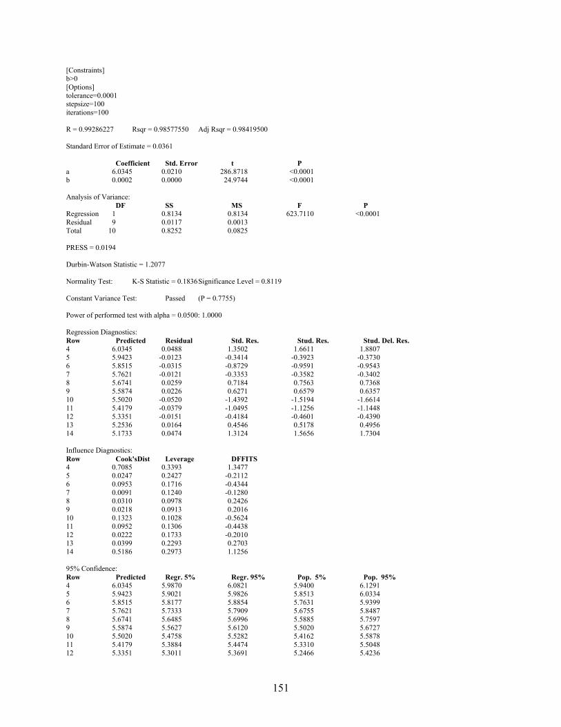
151
[Constraints] b>0 [Options] tolerance=0.0001 stepsize=100 iterations=100 R = 0.99286227 Rsqr = 0.98577550 Adj Rsqr = 0.98419500 Standard Error of Estimate = 0.0361 Coefficient Std. Error t P a 6.0345 0.0210 286.8718 <0.0001 b 0.0002 0.0000 24.9744 <0.0001 Analysis of Variance: DF SS MS F P Regression 1 0.8134 0.8134 623.7110 <0.0001 Residual 9 0.0117 0.0013 Total 10 0.8252 0.0825 PRESS = 0.0194 Durbin-Watson Statistic = 1.2077 Normality Test: K-S Statistic = 0.1836 Significance Level = 0.8119 Constant Variance Test: Passed (P = 0.7755) Power of performed test with alpha = 0.0500: 1.0000 Regression Diagnostics: Row Predicted Residual Std. Res. Stud. Res. Stud. Del. Res. 4 6.0345 0.0488 1.3502 1.6611 1.8807 5 5.9423 -0.0123 -0.3414 -0.3923 -0.3730 6 5.8515 -0.0315 -0.8729 -0.9591 -0.9543 7 5.7621 -0.0121 -0.3353 -0.3582 -0.3402 8 5.6741 0.0259 0.7184 0.7563 0.7368 9 5.5874 0.0226 0.6271 0.6579 0.6357 10 5.5020 -0.0520 -1.4392 -1.5194 -1.6614 11 5.4179 -0.0379 -1.0495 -1.1256 -1.1448 12 5.3351 -0.0151 -0.4184 -0.4601 -0.4390 13 5.2536 0.0164 0.4546 0.5178 0.4956 14 5.1733 0.0474 1.3124 1.5656 1.7304 Influence Diagnostics: Row Cook'sDist Leverage DFFITS 4 0.7085 0.3393 1.3477 5 0.0247 0.2427 -0.2112 6 0.0953 0.1716 -0.4344 7 0.0091 0.1240 -0.1280 8 0.0310 0.0978 0.2426 9 0.0218 0.0913 0.2016 10 0.1323 0.1028 -0.5624 11 0.0952 0.1306 -0.4438 12 0.0222 0.1733 -0.2010 13 0.0399 0.2293 0.2703 14 0.5186 0.2973 1.1256 95% Confidence: Row Predicted Regr. 5% Regr. 95% Pop. 5% Pop. 95% 4 6.0345 5.9870 6.0821 5.9400 6.1291 5 5.9423 5.9021 5.9826 5.8513 6.0334 6 5.8515 5.8177 5.8854 5.7631 5.9399 7 5.7621 5.7333 5.7909 5.6755 5.8487 8 5.6741 5.6485 5.6996 5.5885 5.7597 9 5.5874 5.5627 5.6120 5.5020 5.6727 10 5.5020 5.4758 5.5282 5.4162 5.5878 11 5.4179 5.3884 5.4474 5.3310 5.5048 12 5.3351 5.3011 5.3691 5.2466 5.4236
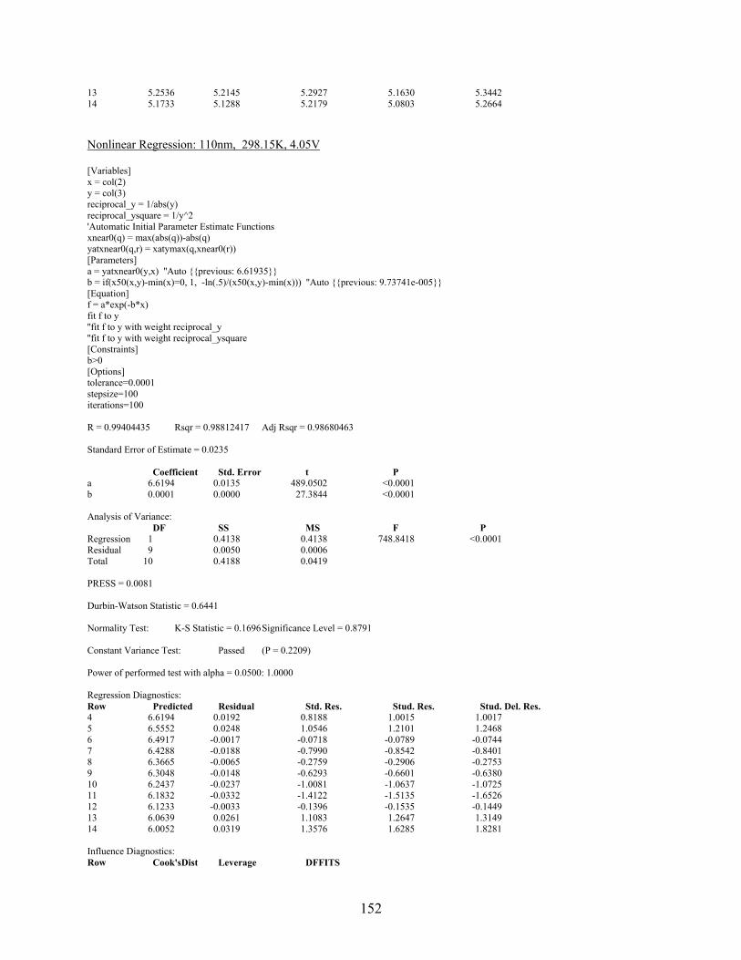
152
13 5.2536 5.2145 5.2927 5.1630 5.3442 14 5.1733 5.1288 5.2179 5.0803 5.2664 Nonlinear Regression: 110nm, 298.15K, 4.05V [Variables] x = col(2) y = col(3) reciprocal_y = 1/abs(y) reciprocal_ysquare = 1/y^2 'Automatic Initial Parameter Estimate Functions xnear0(q) = max(abs(q))-abs(q) yatxnear0(q,r) = xatymax(q,xnear0(r)) [Parameters] a = yatxnear0(y,x) ''Auto previous: 6.61935 b = if(x50(x,y)-min(x)=0, 1, -ln(.5)/(x50(x,y)-min(x))) ''Auto previous: 9.73741e-005 [Equation] f = a*exp(-b*x) fit f to y ''fit f to y with weight reciprocal_y ''fit f to y with weight reciprocal_ysquare [Constraints] b>0 [Options] tolerance=0.0001 stepsize=100 iterations=100 R = 0.99404435 Rsqr = 0.98812417 Adj Rsqr = 0.98680463 Standard Error of Estimate = 0.0235 Coefficient Std. Error t P a 6.6194 0.0135 489.0502 <0.0001 b 0.0001 0.0000 27.3844 <0.0001 Analysis of Variance: DF SS MS F P Regression 1 0.4138 0.4138 748.8418 <0.0001 Residual 9 0.0050 0.0006 Total 10 0.4188 0.0419 PRESS = 0.0081 Durbin-Watson Statistic = 0.6441 Normality Test: K-S Statistic = 0.1696 Significance Level = 0.8791 Constant Variance Test: Passed (P = 0.2209) Power of performed test with alpha = 0.0500: 1.0000 Regression Diagnostics: Row Predicted Residual Std. Res. Stud. Res. Stud. Del. Res. 4 6.6194 0.0192 0.8188 1.0015 1.0017 5 6.5552 0.0248 1.0546 1.2101 1.2468 6 6.4917 -0.0017 -0.0718 -0.0789 -0.0744 7 6.4288 -0.0188 -0.7990 -0.8542 -0.8401 8 6.3665 -0.0065 -0.2759 -0.2906 -0.2753 9 6.3048 -0.0148 -0.6293 -0.6601 -0.6380 10 6.2437 -0.0237 -1.0081 -1.0637 -1.0725 11 6.1832 -0.0332 -1.4122 -1.5135 -1.6526 12 6.1233 -0.0033 -0.1396 -0.1535 -0.1449 13 6.0639 0.0261 1.1083 1.2647 1.3149 14 6.0052 0.0319 1.3576 1.6285 1.8281 Influence Diagnostics: Row Cook'sDist Leverage DFFITS
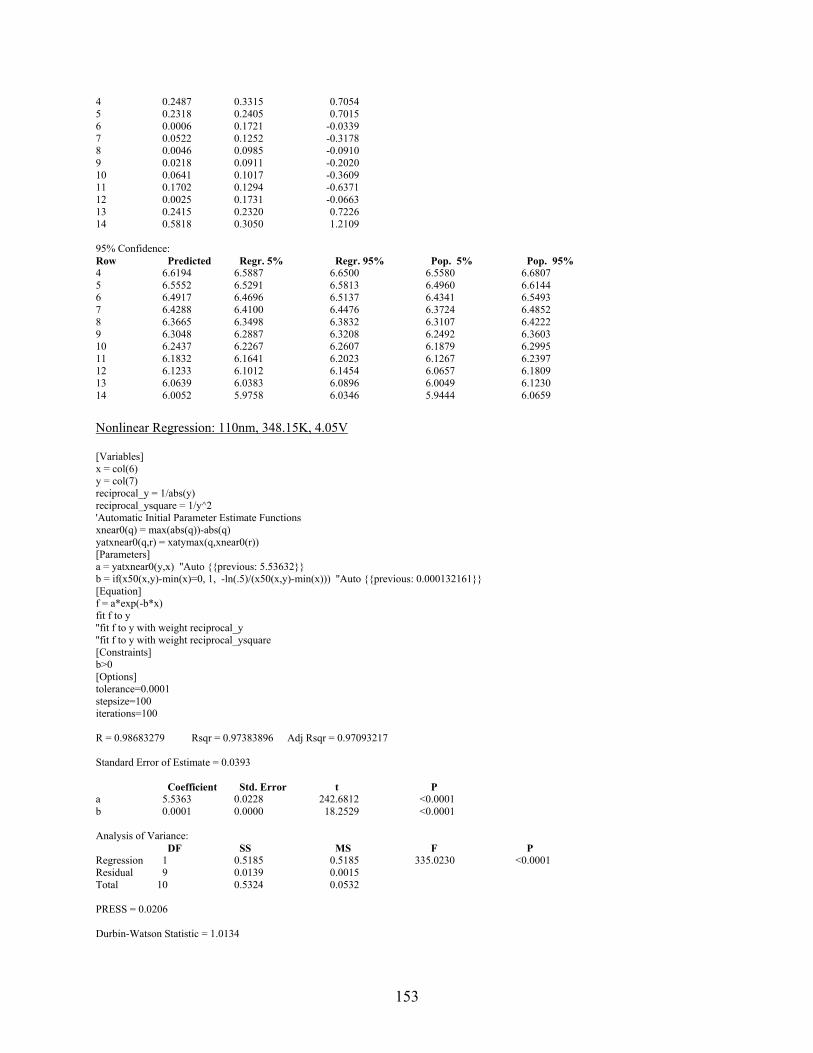
153
4 0.2487 0.3315 0.7054 5 0.2318 0.2405 0.7015 6 0.0006 0.1721 -0.0339 7 0.0522 0.1252 -0.3178 8 0.0046 0.0985 -0.0910 9 0.0218 0.0911 -0.2020 10 0.0641 0.1017 -0.3609 11 0.1702 0.1294 -0.6371 12 0.0025 0.1731 -0.0663 13 0.2415 0.2320 0.7226 14 0.5818 0.3050 1.2109 95% Confidence: Row Predicted Regr. 5% Regr. 95% Pop. 5% Pop. 95% 4 6.6194 6.5887 6.6500 6.5580 6.6807 5 6.5552 6.5291 6.5813 6.4960 6.6144 6 6.4917 6.4696 6.5137 6.4341 6.5493 7 6.4288 6.4100 6.4476 6.3724 6.4852 8 6.3665 6.3498 6.3832 6.3107 6.4222 9 6.3048 6.2887 6.3208 6.2492 6.3603 10 6.2437 6.2267 6.2607 6.1879 6.2995 11 6.1832 6.1641 6.2023 6.1267 6.2397 12 6.1233 6.1012 6.1454 6.0657 6.1809 13 6.0639 6.0383 6.0896 6.0049 6.1230 14 6.0052 5.9758 6.0346 5.9444 6.0659 Nonlinear Regression: 110nm, 348.15K, 4.05V [Variables] x = col(6) y = col(7) reciprocal_y = 1/abs(y) reciprocal_ysquare = 1/y^2 'Automatic Initial Parameter Estimate Functions xnear0(q) = max(abs(q))-abs(q) yatxnear0(q,r) = xatymax(q,xnear0(r)) [Parameters] a = yatxnear0(y,x) ''Auto previous: 5.53632 b = if(x50(x,y)-min(x)=0, 1, -ln(.5)/(x50(x,y)-min(x))) ''Auto previous: 0.000132161 [Equation] f = a*exp(-b*x) fit f to y ''fit f to y with weight reciprocal_y ''fit f to y with weight reciprocal_ysquare [Constraints] b>0 [Options] tolerance=0.0001 stepsize=100 iterations=100 R = 0.98683279 Rsqr = 0.97383896 Adj Rsqr = 0.97093217 Standard Error of Estimate = 0.0393 Coefficient Std. Error t P a 5.5363 0.0228 242.6812 <0.0001 b 0.0001 0.0000 18.2529 <0.0001 Analysis of Variance: DF SS MS F P Regression 1 0.5185 0.5185 335.0230 <0.0001 Residual 9 0.0139 0.0015 Total 10 0.5324 0.0532 PRESS = 0.0206 Durbin-Watson Statistic = 1.0134
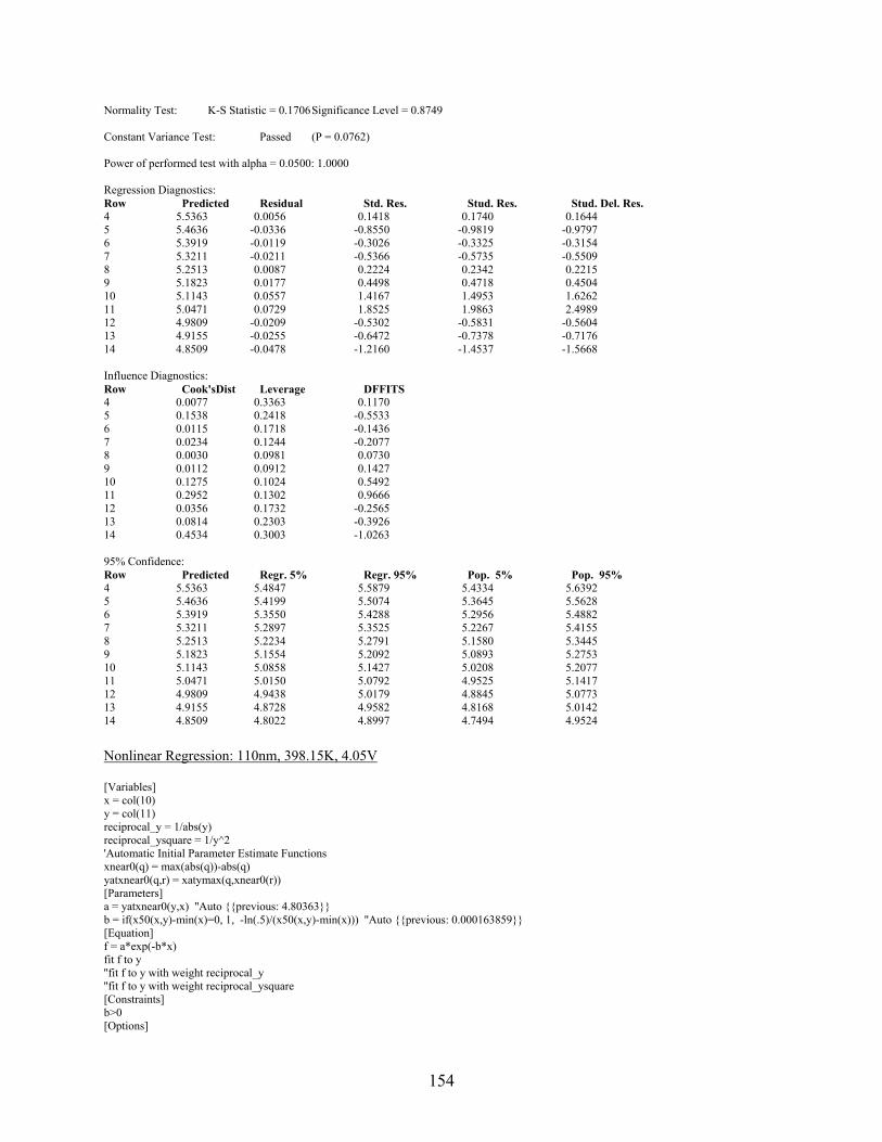
154
Normality Test: K-S Statistic = 0.1706 Significance Level = 0.8749 Constant Variance Test: Passed (P = 0.0762) Power of performed test with alpha = 0.0500: 1.0000 Regression Diagnostics: Row Predicted Residual Std. Res. Stud. Res. Stud. Del. Res. 4 5.5363 0.0056 0.1418 0.1740 0.1644 5 5.4636 -0.0336 -0.8550 -0.9819 -0.9797 6 5.3919 -0.0119 -0.3026 -0.3325 -0.3154 7 5.3211 -0.0211 -0.5366 -0.5735 -0.5509 8 5.2513 0.0087 0.2224 0.2342 0.2215 9 5.1823 0.0177 0.4498 0.4718 0.4504 10 5.1143 0.0557 1.4167 1.4953 1.6262 11 5.0471 0.0729 1.8525 1.9863 2.4989 12 4.9809 -0.0209 -0.5302 -0.5831 -0.5604 13 4.9155 -0.0255 -0.6472 -0.7378 -0.7176 14 4.8509 -0.0478 -1.2160 -1.4537 -1.5668 Influence Diagnostics: Row Cook'sDist Leverage DFFITS 4 0.0077 0.3363 0.1170 5 0.1538 0.2418 -0.5533 6 0.0115 0.1718 -0.1436 7 0.0234 0.1244 -0.2077 8 0.0030 0.0981 0.0730 9 0.0112 0.0912 0.1427 10 0.1275 0.1024 0.5492 11 0.2952 0.1302 0.9666 12 0.0356 0.1732 -0.2565 13 0.0814 0.2303 -0.3926 14 0.4534 0.3003 -1.0263 95% Confidence: Row Predicted Regr. 5% Regr. 95% Pop. 5% Pop. 95% 4 5.5363 5.4847 5.5879 5.4334 5.6392 5 5.4636 5.4199 5.5074 5.3645 5.5628 6 5.3919 5.3550 5.4288 5.2956 5.4882 7 5.3211 5.2897 5.3525 5.2267 5.4155 8 5.2513 5.2234 5.2791 5.1580 5.3445 9 5.1823 5.1554 5.2092 5.0893 5.2753 10 5.1143 5.0858 5.1427 5.0208 5.2077 11 5.0471 5.0150 5.0792 4.9525 5.1417 12 4.9809 4.9438 5.0179 4.8845 5.0773 13 4.9155 4.8728 4.9582 4.8168 5.0142 14 4.8509 4.8022 4.8997 4.7494 4.9524 Nonlinear Regression: 110nm, 398.15K, 4.05V [Variables] x = col(10) y = col(11) reciprocal_y = 1/abs(y) reciprocal_ysquare = 1/y^2 'Automatic Initial Parameter Estimate Functions xnear0(q) = max(abs(q))-abs(q) yatxnear0(q,r) = xatymax(q,xnear0(r)) [Parameters] a = yatxnear0(y,x) ''Auto previous: 4.80363 b = if(x50(x,y)-min(x)=0, 1, -ln(.5)/(x50(x,y)-min(x))) ''Auto previous: 0.000163859 [Equation] f = a*exp(-b*x) fit f to y ''fit f to y with weight reciprocal_y ''fit f to y with weight reciprocal_ysquare [Constraints] b>0 [Options]

155
tolerance=0.0001 stepsize=100 iterations=100 R = 0.99731150 Rsqr = 0.99463023 Adj Rsqr = 0.99403359 Standard Error of Estimate = 0.0186 Coefficient Std. Error t P a 4.8036 0.0109 441.6168 <0.0001 b 0.0002 0.0000 40.7878 <0.0001 Analysis of Variance: DF SS MS F P Regression 1 0.5790 0.5790 1667.0493 <0.0001 Residual 9 0.0031 0.0003 Total 10 0.5821 0.0582 PRESS = 0.0057 Durbin-Watson Statistic = 1.4607 Normality Test: K-S Statistic = 0.2475 Significance Level = 0.4523 Constant Variance Test: Passed (P = 0.0883) Power of performed test with alpha = 0.0500: 1.0000 Regression Diagnostics: Row Predicted Residual Std. Res. Stud. Res. Stud. Del. Res. 4 4.8036 0.0372 1.9942 2.4560 4.0320 5 4.7256 -0.0156 -0.8352 -0.9599 -0.9553 6 4.6488 -0.0188 -1.0068 -1.1061 -1.1219 7 4.5732 -0.0132 -0.7088 -0.7572 -0.7378 8 4.4989 -0.0089 -0.4767 -0.5019 -0.4799 9 4.4258 -0.0058 -0.3094 -0.3246 -0.3079 10 4.3538 0.0162 0.8672 0.9157 0.9066 11 4.2831 0.0169 0.9080 0.9740 0.9709 12 4.2135 -0.0135 -0.7226 -0.7948 -0.7771 13 4.1450 -0.0050 -0.2677 -0.3048 -0.2889 14 4.0776 0.0105 0.5622 0.6700 0.6481 Influence Diagnostics: Row Cook'sDist Leverage DFFITS 4 1.5582 0.3407 2.8982 5 0.1480 0.2431 -0.5413 6 0.1266 0.1715 -0.5104 7 0.0405 0.1237 -0.2773 8 0.0136 0.0977 -0.1579 9 0.0053 0.0914 -0.0976 10 0.0482 0.1030 0.3072 11 0.0714 0.1308 0.3767 12 0.0662 0.1733 -0.3557 13 0.0138 0.2288 -0.1573 14 0.0944 0.2960 0.4202 95% Confidence: Row Predicted Regr. 5% Regr. 95% Pop. 5% Pop. 95% 4 4.8036 4.7790 4.8282 4.7548 4.8524 5 4.7256 4.7048 4.7463 4.6786 4.7726 6 4.6488 4.6313 4.6662 4.6031 4.6944 7 4.5732 4.5584 4.5880 4.5285 4.6179 8 4.4989 4.4857 4.5121 4.4547 4.5431 9 4.4258 4.4130 4.4385 4.3817 4.4698 10 4.3538 4.3403 4.3674 4.3096 4.3981 11 4.2831 4.2678 4.2983 4.2382 4.3279 12 4.2135 4.1959 4.2310 4.1678 4.2591 13 4.1450 4.1248 4.1652 4.0983 4.1917 14 4.0776 4.0547 4.1006 4.0296 4.1256
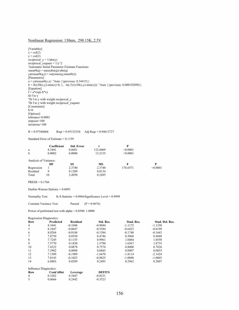
156
Nonlinear Regression: 130nm, 298.15K, 2.5V [Variables] x = col(2) y = col(3) reciprocal_y = 1/abs(y) reciprocal_ysquare = 1/y^2 'Automatic Initial Parameter Estimate Functions xnear0(q) = max(abs(q))-abs(q) yatxnear0(q,r) = xatymax(q,xnear0(r)) [Parameters] a = yatxnear0(y,x) ''Auto previous: 8.34415 b = if(x50(x,y)-min(x)=0, 1, -ln(.5)/(x50(x,y)-min(x))) ''Auto previous: 0.000192898 [Equation] f = a*exp(-b*x) fit f to y ''fit f to y with weight reciprocal_y ''fit f to y with weight reciprocal_ysquare [Constraints] b>0 [Options] tolerance=0.0001 stepsize=100 iterations=100 R = 0.97546068 Rsqr = 0.95152354 Adj Rsqr = 0.94613727 Standard Error of Estimate = 0.1159 Coefficient Std. Error t P a 8.3441 0.0681 122.6069 <0.0001 b 0.0002 0.0000 13.2135 <0.0001 Analysis of Variance: DF SS MS F P Regression 1 2.3740 2.3740 176.6571 <0.0001 Residual 9 0.1209 0.0134 Total 10 2.4950 0.2495 PRESS = 0.1766 Durbin-Watson Statistic = 0.8093 Normality Test: K-S Statistic = 0.0966 Significance Level = 0.9999 Constant Variance Test: Passed (P = 0.9676) Power of performed test with alpha = 0.0500: 1.0000 Regression Diagnostics: Row Predicted Residual Std. Res. Stud. Res. Stud. Del. Res. 4 8.3441 -0.1048 -0.9044 -1.1172 -1.1350 5 8.1847 -0.0647 -0.5584 -0.6423 -0.6199 6 8.0284 -0.0184 -0.1584 -0.1740 -0.1643 7 7.8750 0.0550 0.4746 0.5068 0.4848 8 7.7245 0.1155 0.9961 1.0484 1.0550 9 7.5770 0.1830 1.5790 1.6567 1.8735 10 7.4322 0.0878 0.7574 0.8000 0.7826 11 7.2902 0.0098 0.0845 0.0907 0.0855 12 7.1509 -0.1909 -1.6470 -1.8114 -2.1424 13 7.0143 -0.1023 -0.8825 -1.0040 -1.0045 14 6.8803 0.0289 0.2493 0.2963 0.2807 Influence Diagnostics: Row Cook'sDist Leverage DFFITS 4 0.3282 0.3447 -0.8231 5 0.0666 0.2442 -0.3523
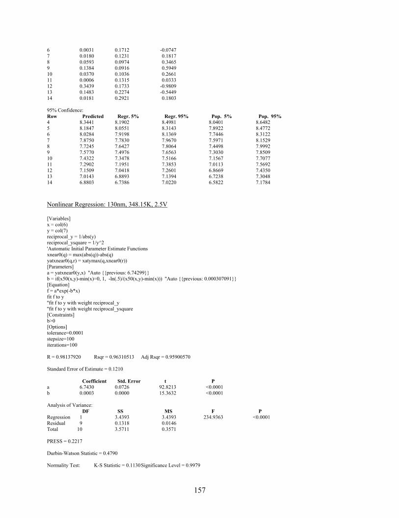
157
6 0.0031 0.1712 -0.0747 7 0.0180 0.1231 0.1817 8 0.0593 0.0974 0.3465 9 0.1384 0.0916 0.5949 10 0.0370 0.1036 0.2661 11 0.0006 0.1315 0.0333 12 0.3439 0.1733 -0.9809 13 0.1483 0.2274 -0.5449 14 0.0181 0.2921 0.1803 95% Confidence: Row Predicted Regr. 5% Regr. 95% Pop. 5% Pop. 95% 4 8.3441 8.1902 8.4981 8.0401 8.6482 5 8.1847 8.0551 8.3143 7.8922 8.4772 6 8.0284 7.9198 8.1369 7.7446 8.3122 7 7.8750 7.7830 7.9670 7.5971 8.1529 8 7.7245 7.6427 7.8064 7.4498 7.9992 9 7.5770 7.4976 7.6563 7.3030 7.8509 10 7.4322 7.3478 7.5166 7.1567 7.7077 11 7.2902 7.1951 7.3853 7.0113 7.5692 12 7.1509 7.0418 7.2601 6.8669 7.4350 13 7.0143 6.8893 7.1394 6.7238 7.3048 14 6.8803 6.7386 7.0220 6.5822 7.1784 Nonlinear Regression: 130nm, 348.15K, 2.5V [Variables] x = col(6) y = col(7) reciprocal_y = 1/abs(y) reciprocal_ysquare = 1/y^2 'Automatic Initial Parameter Estimate Functions xnear0(q) = max(abs(q))-abs(q) yatxnear0(q,r) = xatymax(q,xnear0(r)) [Parameters] a = yatxnear0(y,x) ''Auto previous: 6.74299 b = if(x50(x,y)-min(x)=0, 1, -ln(.5)/(x50(x,y)-min(x))) ''Auto previous: 0.000307091 [Equation] f = a*exp(-b*x) fit f to y ''fit f to y with weight reciprocal_y ''fit f to y with weight reciprocal_ysquare [Constraints] b>0 [Options] tolerance=0.0001 stepsize=100 iterations=100 R = 0.98137920 Rsqr = 0.96310513 Adj Rsqr = 0.95900570 Standard Error of Estimate = 0.1210 Coefficient Std. Error t P a 6.7430 0.0726 92.8213 <0.0001 b 0.0003 0.0000 15.3632 <0.0001 Analysis of Variance: DF SS MS F P Regression 1 3.4393 3.4393 234.9363 <0.0001 Residual 9 0.1318 0.0146 Total 10 3.5711 0.3571 PRESS = 0.2217 Durbin-Watson Statistic = 0.4790 Normality Test: K-S Statistic = 0.1130 Significance Level = 0.9979
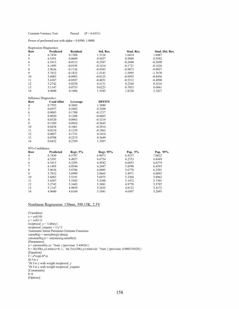
158
Constant Variance Test: Passed (P = 0.6531) Power of performed test with alpha = 0.0500: 1.0000 Regression Diagnostics: Row Predicted Residual Std. Res. Stud. Res. Stud. Del. Res. 4 6.7430 0.1588 1.3126 1.6414 1.8487 5 6.5391 0.0609 0.5037 0.5809 0.5582 6 6.3413 -0.0313 -0.2587 -0.2840 -0.2690 7 6.1495 -0.0195 -0.1614 -0.1721 -0.1626 8 5.9636 -0.1136 -0.9385 -0.9873 -0.9857 9 5.7832 -0.1832 -1.5141 -1.5895 -1.7670 10 5.6083 -0.0983 -0.8125 -0.8593 -0.8456 11 5.4387 -0.0587 -0.4851 -0.5212 -0.4990 12 5.2742 0.0258 0.2131 0.2344 0.2216 13 5.1147 0.0753 0.6223 0.7053 0.6841 14 4.9600 0.1886 1.5585 1.8328 2.1827 Influence Diagnostics: Row Cook'sDist Leverage DFFITS 4 0.7593 0.3605 1.3880 5 0.0557 0.2482 0.3208 6 0.0083 0.1700 -0.1217 7 0.0020 0.1208 -0.0603 8 0.0520 0.0963 -0.3219 9 0.1289 0.0926 -0.5645 10 0.0438 0.1061 -0.2914 11 0.0210 0.1339 -0.1962 12 0.0057 0.1731 0.1014 13 0.0708 0.2215 0.3649 14 0.6432 0.2769 1.3507 95% Confidence: Row Predicted Regr. 5% Regr. 95% Pop. 5% Pop. 95% 4 6.7430 6.5787 6.9073 6.4237 7.0622 5 6.5391 6.4027 6.6754 6.2333 6.8449 6 6.3413 6.2285 6.4542 6.0452 6.6374 7 6.1495 6.0544 6.2447 5.8598 6.4393 8 5.9636 5.8786 6.0485 5.6770 6.2501 9 5.7832 5.6999 5.8665 5.4971 6.0693 10 5.6083 5.5191 5.6975 5.3204 5.8962 11 5.4387 5.3385 5.5388 5.1472 5.7301 12 5.2742 5.1603 5.3881 4.9778 5.5707 13 5.1147 4.9859 5.2435 4.8122 5.4172 14 4.9600 4.8160 5.1041 4.6507 5.2693 Nonlinear Regression: 130nm, 398.15K, 2.5V [Variables] x = col(10) y = col(11) reciprocal_y = 1/abs(y) reciprocal_ysquare = 1/y^2 'Automatic Initial Parameter Estimate Functions xnear0(q) = max(abs(q))-abs(q) yatxnear0(q,r) = xatymax(q,xnear0(r)) [Parameters] a = yatxnear0(y,x) ''Auto previous: 5.44426 b = if(x50(x,y)-min(x)=0, 1, -ln(.5)/(x50(x,y)-min(x))) ''Auto previous: 0.000319428 [Equation] f = a*exp(-b*x) fit f to y ''fit f to y with weight reciprocal_y ''fit f to y with weight reciprocal_ysquare [Constraints] b>0 [Options]
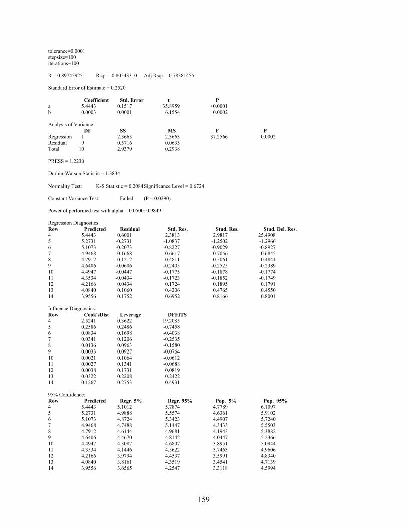
159
tolerance=0.0001 stepsize=100 iterations=100 R = 0.89745925 Rsqr = 0.80543310 Adj Rsqr = 0.78381455 Standard Error of Estimate = 0.2520 Coefficient Std. Error t P a 5.4443 0.1517 35.8959 <0.0001 b 0.0003 0.0001 6.1554 0.0002 Analysis of Variance: DF SS MS F P Regression 1 2.3663 2.3663 37.2566 0.0002 Residual 9 0.5716 0.0635 Total 10 2.9379 0.2938 PRESS = 1.2230 Durbin-Watson Statistic = 1.3834 Normality Test: K-S Statistic = 0.2084 Significance Level = 0.6724 Constant Variance Test: Failed (P = 0.0290) Power of performed test with alpha = 0.0500: 0.9849 Regression Diagnostics: Row Predicted Residual Std. Res. Stud. Res. Stud. Del. Res. 4 5.4443 0.6001 2.3813 2.9817 25.4908 5 5.2731 -0.2731 -1.0837 -1.2502 -1.2966 6 5.1073 -0.2073 -0.8227 -0.9029 -0.8927 7 4.9468 -0.1668 -0.6617 -0.7056 -0.6845 8 4.7912 -0.1212 -0.4811 -0.5061 -0.4841 9 4.6406 -0.0606 -0.2405 -0.2525 -0.2389 10 4.4947 -0.0447 -0.1775 -0.1878 -0.1774 11 4.3534 -0.0434 -0.1723 -0.1852 -0.1749 12 4.2166 0.0434 0.1724 0.1895 0.1791 13 4.0840 0.1060 0.4206 0.4765 0.4550 14 3.9556 0.1752 0.6952 0.8166 0.8001 Influence Diagnostics: Row Cook'sDist Leverage DFFITS 4 2.5241 0.3622 19.2085 5 0.2586 0.2486 -0.7458 6 0.0834 0.1698 -0.4038 7 0.0341 0.1206 -0.2535 8 0.0136 0.0963 -0.1580 9 0.0033 0.0927 -0.0764 10 0.0021 0.1064 -0.0612 11 0.0027 0.1341 -0.0688 12 0.0038 0.1731 0.0819 13 0.0322 0.2208 0.2422 14 0.1267 0.2753 0.4931 95% Confidence: Row Predicted Regr. 5% Regr. 95% Pop. 5% Pop. 95% 4 5.4443 5.1012 5.7874 4.7789 6.1097 5 5.2731 4.9888 5.5574 4.6361 5.9102 6 5.1073 4.8724 5.3423 4.4907 5.7240 7 4.9468 4.7488 5.1447 4.3433 5.5503 8 4.7912 4.6144 4.9681 4.1943 5.3882 9 4.6406 4.4670 4.8142 4.0447 5.2366 10 4.4947 4.3087 4.6807 3.8951 5.0944 11 4.3534 4.1446 4.5622 3.7463 4.9606 12 4.2166 3.9794 4.4537 3.5991 4.8340 13 4.0840 3.8161 4.3519 3.4541 4.7139 14 3.9556 3.6565 4.2547 3.3118 4.5994
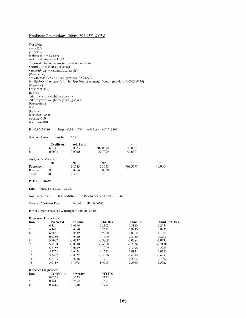
160
Nonlinear Regression: 130nm, 298.15K, 4.05V [Variables] x = col(2) y = col(3) reciprocal_y = 1/abs(y) reciprocal_ysquare = 1/y^2 'Automatic Initial Parameter Estimate Functions xnear0(q) = max(abs(q))-abs(q) yatxnear0(q,r) = xatymax(q,xnear0(r)) [Parameters] a = yatxnear0(y,x) ''Auto previous: 6.52409 b = if(x50(x,y)-min(x)=0, 1, -ln(.5)/(x50(x,y)-min(x))) ''Auto previous: 0.000249826 [Equation] f = a*exp(-b*x) fit f to y ''fit f to y with weight reciprocal_y ''fit f to y with weight reciprocal_ysquare [Constraints] b>0 [Options] tolerance=0.0001 stepsize=100 iterations=100 R = 0.99420186 Rsqr = 0.98843734 Adj Rsqr = 0.98715260 Standard Error of Estimate = 0.0544 Coefficient Std. Error t P a 6.5241 0.0323 202.0870 <0.0001 b 0.0002 0.0000 27.7099 <0.0001 Analysis of Variance: DF SS MS F P Regression 1 2.2745 2.2745 769.3677 <0.0001 Residual 9 0.0266 0.0030 Total 10 2.3011 0.2301 PRESS = 0.0437 Durbin-Watson Statistic = 0.8986 Normality Test: K-S Statistic = 0.1885 Significance Level = 0.7860 Constant Variance Test: Passed (P = 0.9676) Power of performed test with alpha = 0.0500: 1.0000 Regression Diagnostics: Row Predicted Residual Std. Res. Stud. Res. Stud. Del. Res. 4 6.5241 0.0136 0.2502 0.3110 0.2948 5 6.3631 0.0469 0.8621 0.9930 0.9922 6 6.2061 0.0539 0.9908 1.0880 1.1007 7 6.0530 -0.0430 -0.7909 -0.8440 -0.8293 8 5.9037 -0.0537 -0.9868 -1.0384 -1.0435 9 5.7580 -0.0380 -0.6988 -0.7334 -0.7130 10 5.6159 -0.0159 -0.2929 -0.3096 -0.2935 11 5.4774 -0.0474 -0.8711 -0.9354 -0.9282 12 5.3422 -0.0322 -0.5926 -0.6518 -0.6295 13 5.2104 0.0096 0.1763 0.2002 0.1892 14 5.0819 0.1073 1.9743 2.3340 3.5025 Influence Diagnostics: Row Cook'sDist Leverage DFFITS 4 0.0263 0.3525 0.2175 5 0.1611 0.2462 0.5671 6 0.1218 0.1706 0.4993
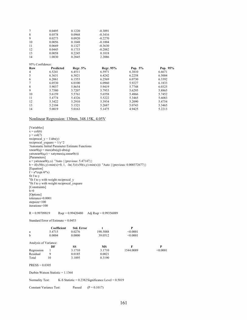
161
7 0.0495 0.1220 -0.3091 8 0.0578 0.0968 -0.3416 9 0.0273 0.0920 -0.2270 10 0.0056 0.1048 -0.1004 11 0.0669 0.1327 -0.3630 12 0.0445 0.1733 -0.2882 13 0.0058 0.2245 0.1018 14 1.0830 0.2845 2.2086 95% Confidence: Row Predicted Regr. 5% Regr. 95% Pop. 5% Pop. 95% 4 6.5241 6.4511 6.5971 6.3810 6.6671 5 6.3631 6.3021 6.4242 6.2258 6.5004 6 6.2061 6.1553 6.2569 6.0730 6.3392 7 6.0530 6.0100 6.0960 5.9227 6.1833 8 5.9037 5.8654 5.9419 5.7748 6.0325 9 5.7580 5.7207 5.7953 5.6295 5.8865 10 5.6159 5.5761 5.6558 5.4866 5.7452 11 5.4774 5.4326 5.5222 5.3465 5.6083 12 5.3422 5.2910 5.3934 5.2090 5.4754 13 5.2104 5.1521 5.2687 5.0743 5.3465 14 5.0819 5.0163 5.1475 4.9425 5.2213 Nonlinear Regression: 130nm, 348.15K, 4.05V [Variables] x = col(6) y = col(7) reciprocal_y = 1/abs(y) reciprocal_ysquare = 1/y^2 'Automatic Initial Parameter Estimate Functions xnear0(q) = max(abs(q))-abs(q) yatxnear0(q,r) = xatymax(q,xnear0(r)) [Parameters] a = yatxnear0(y,x) ''Auto previous: 5.47147 b = if(x50(x,y)-min(x)=0, 1, -ln(.5)/(x50(x,y)-min(x))) ''Auto previous: 0.000372677 [Equation] f = a*exp(-b*x) fit f to y ''fit f to y with weight reciprocal_y ''fit f to y with weight reciprocal_ysquare [Constraints] b>0 [Options] tolerance=0.0001 stepsize=100 iterations=100 R = 0.99709819 Rsqr = 0.99420480 Adj Rsqr = 0.99356089 Standard Error of Estimate = 0.0453 Coefficient Std. Error t P a 5.4715 0.0276 198.5888 <0.0001 b 0.0004 0.0000 39.0512 <0.0001 Analysis of Variance: DF SS MS F P Regression 1 3.1710 3.1710 1544.0089 <0.0001 Residual 9 0.0185 0.0021 Total 10 3.1895 0.3190 PRESS = 0.0305 Durbin-Watson Statistic = 1.1364 Normality Test: K-S Statistic = 0.2382 Significance Level = 0.5019 Constant Variance Test: Passed (P = 0.1017)
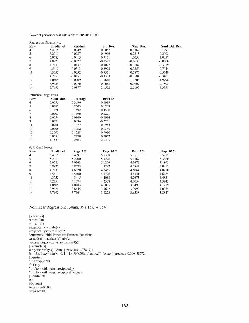
162
Power of performed test with alpha = 0.0500: 1.0000 Regression Diagnostics: Row Predicted Residual Std. Res. Stud. Res. Stud. Del. Res. 4 5.4715 0.0049 0.1087 0.1369 0.1292 5 5.2713 0.0087 0.1916 0.2213 0.2092 6 5.0785 0.0415 0.9161 1.0050 1.0057 7 4.8927 -0.0027 -0.0597 -0.0636 -0.0600 8 4.7137 -0.0137 -0.3027 -0.3184 -0.3019 9 4.5413 -0.0313 -0.6903 -0.7250 -0.7044 10 4.3752 -0.0252 -0.5551 -0.5876 -0.5649 11 4.2151 -0.0151 -0.3333 -0.3584 -0.3403 12 4.0609 -0.0709 -1.5646 -1.7203 -1.9798 13 3.9124 0.0076 0.1688 0.1909 0.1803 14 3.7692 0.0977 2.1552 2.5195 4.3758 Influence Diagnostics: Row Cook'sDist Leverage DFFITS 4 0.0055 0.3696 0.0989 5 0.0082 0.2503 0.1209 6 0.1028 0.1692 0.4538 7 0.0003 0.1196 -0.0221 8 0.0054 0.0960 -0.0984 9 0.0271 0.0934 -0.2261 10 0.0208 0.1077 -0.1963 11 0.0100 0.1352 -0.1346 12 0.3092 0.1728 -0.9050 13 0.0051 0.2179 0.0952 14 1.1637 0.2683 2.6495 95% Confidence: Row Predicted Regr. 5% Regr. 95% Pop. 5% Pop. 95% 4 5.4715 5.4091 5.5338 5.3515 5.5915 5 5.2713 5.2200 5.3226 5.1567 5.3860 6 5.0785 5.0363 5.1206 4.9676 5.1893 7 4.8927 4.8573 4.9282 4.7842 5.0012 8 4.7137 4.6820 4.7455 4.6064 4.8210 9 4.5413 4.5100 4.5726 4.4341 4.6485 10 4.3752 4.3415 4.4088 4.2673 4.4831 11 4.2151 4.1774 4.2528 4.1059 4.3243 12 4.0609 4.0183 4.1035 3.9499 4.1719 13 3.9124 3.8645 3.9602 3.7992 4.0255 14 3.7692 3.7161 3.8223 3.6538 3.8847 Nonlinear Regression: 130nm, 398.15K, 4.05V [Variables] x = col(10) y = col(11) reciprocal_y = 1/abs(y) reciprocal_ysquare = 1/y^2 'Automatic Initial Parameter Estimate Functions xnear0(q) = max(abs(q))-abs(q) yatxnear0(q,r) = xatymax(q,xnear0(r)) [Parameters] a = yatxnear0(y,x) ''Auto previous: 4.75819 b = if(x50(x,y)-min(x)=0, 1, -ln(.5)/(x50(x,y)-min(x))) ''Auto previous: 0.000438572 [Equation] f = a*exp(-b*x) fit f to y ''fit f to y with weight reciprocal_y ''fit f to y with weight reciprocal_ysquare [Constraints] b>0 [Options] tolerance=0.0001 stepsize=100
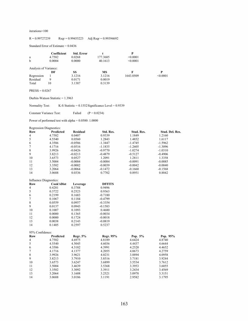
163
iterations=100 R = 0.99727239 Rsqr = 0.99455223 Adj Rsqr = 0.99394692 Standard Error of Estimate = 0.0436 Coefficient Std. Error t P a 4.7582 0.0268 177.3685 <0.0001 b 0.0004 0.0000 40.1613 <0.0001 Analysis of Variance: DF SS MS F P Regression 1 3.1216 3.1216 1643.0509 <0.0001 Residual 9 0.0171 0.0019 Total 10 3.1387 0.3139 PRESS = 0.0267 Durbin-Watson Statistic = 1.3963 Normality Test: K-S Statistic = 0.1552 Significance Level = 0.9339 Constant Variance Test: Failed (P = 0.0234) Power of performed test with alpha = 0.0500: 1.0000 Regression Diagnostics: Row Predicted Residual Std. Res. Stud. Res. Stud. Del. Res. 4 4.7582 0.0407 0.9339 1.1849 1.2160 5 4.5540 0.0560 1.2843 1.4852 1.6117 6 4.3586 -0.0586 -1.3447 -1.4745 -1.5962 7 4.1716 -0.0516 -1.1835 -1.2605 -1.3096 8 3.9926 -0.0426 -0.9770 -1.0274 -1.0310 9 3.8213 -0.0213 -0.4879 -0.5127 -0.4906 10 3.6573 0.0527 1.2091 1.2811 1.3358 11 3.5004 -0.0004 -0.0084 -0.0091 -0.0085 12 3.3502 -0.0002 -0.0039 -0.0042 -0.0040 13 3.2064 -0.0064 -0.1472 -0.1660 -0.1568 14 3.0688 0.0336 0.7702 0.8951 0.8842 Influence Diagnostics: Row Cook'sDist Leverage DFFITS 4 0.4281 0.3788 0.9496 5 0.3722 0.2523 0.9363 6 0.2199 0.1683 -0.7180 7 0.1067 0.1184 -0.4799 8 0.0559 0.0957 -0.3354 9 0.0137 0.0943 -0.1583 10 0.1007 0.1093 0.4680 11 0.0000 0.1365 -0.0034 12 0.0000 0.1724 -0.0018 13 0.0038 0.2143 -0.0819 14 0.1405 0.2597 0.5237 95% Confidence: Row Predicted Regr. 5% Regr. 95% Pop. 5% Pop. 95% 4 4.7582 4.6975 4.8189 4.6424 4.8740 5 4.5540 4.5045 4.6036 4.4437 4.6644 6 4.3586 4.3182 4.3991 4.2520 4.4652 7 4.1716 4.1377 4.2055 4.0673 4.2759 8 3.9926 3.9621 4.0231 3.8894 4.0958 9 3.8213 3.7910 3.8516 3.7181 3.9244 10 3.6573 3.6247 3.6899 3.5534 3.7612 11 3.5004 3.4639 3.5368 3.3953 3.6055 12 3.3502 3.3092 3.3911 3.2434 3.4569 13 3.2064 3.1608 3.2521 3.0978 3.3151 14 3.0688 3.0186 3.1191 2.9582 3.1795
164
References [1] NASA Jet Propulsion Laboratory Derating Guidelines JPL-D-8545.
[2] J. D. Walter, “Methods to account for accelerated semiconductor device wearout in long life aerospace applications,” UMD Ph.D. Dissertation, 2003.
[3] W. H. Roadstrum and D. H. Wolaver, Electrical Engineering For All Engineers.
Harper & Row, Publishers, Inc, 1987. [4] J. M. Galbraith, et al., “Reliability challenges for low voltage/low power integrated
circuits,” Quality and Reliability Engineering International, vol. 12, pp. 271–279, 1996.
[5] P. Pop, “TDTS 51: Advance computer architecture lecture 11.” /webhttp://www.ida.liu.se/ TDTS51/lectures/lecture11.pdf, 2000.
[6] T. Givargis, “Uci/ics253 lecture 9.”
<www.ics.uci.edu/_givargis/courses/253/notes/lecture9.pdf>, 2002.
[7] W. J. Hsu, et al., “Computer-aided VLSI circuit reliability assurance,” International Journal of Modeling and Simulation, vol. 9, no. 4, pp. 118-123, 1989.
[8] B. S. Chun, et al., “Circuit-level reliability simulation and its applications,” Journal of the Korean Institute of Telematics and Electronics, vol. 31A, no. 1, pp. 93-102, 1994.
[9] S.M. Alam, et al., “Electromigration reliability comparison of Cu and Al interconnects,” Proceedings. 6th International Symposium on Quality Electronic Design, pp. 303-308, 2005.
[10] P. C. Li, et al., “iProbe-d: a hot-carrier and oxide reliability simulator,” 32nd IEEE International Reliability Physics Proceedings, pp. 274-279, 1994.
[11] X. Xuan and A. Chatterjee, “Sensitivity and Reliability Evaluation for Mixed-Signal ICs under Electromigration and Hot-Carrier Effects,” IEEE ISDFT, 2001.
[12] J.W. Lathrop, et al., “Design rules hold key to future VLSI reliability,” Proceedings of the Seventh Biennial University/Government/Industry Microelectronics Symposium, pp. 91-94, 1987.
[13] C. Hu, “Berkeley reliability simulator BERT: An IC reliability simulator,” Microelectronics Journal, vol. 23, no. 2, pp. 97-102, 1992.
[14] W. Bornstein, et al., “Field Degradation of Memory Components from Hot Carriers,” IEEE IRPS, 2006.
[15] University of Maryland - Center for Reliability Engineering, AVSI 17 Project, 2002-2006.
[16] X. Li, et al., “Simulating and Improving Microelectronic Device Reliability by Scaling Voltage and Temperature,” IEEE ISQED, 2005.
165
[17] J. Srinivasan, et al.,"The Impact of Technology Scaling on Lifetime Reliability," International Conference on Dependable Systems and Networks, June 2004.
[18] Failure Mechanisms and Models for Semiconductor Devices. JEDEC Publication JEP122-A, 2002.
[19] S.V. Kumar, et al.,”Impact of NBTI on SRAM Read Stability and Design for Reliability,” IEEE ISQED, 2006.
[20] V. Reddy, et al.,”Impact of NBTI on Digital Circuit Reliability,” IEEE IRPS, 2002.
[21] N.K. Jha, et al.,”NBTI Degradation and its Impact for Analog Circuit Reliability,” IEEE Transactions on Electron Devices, Dec. 2005.
[22] J. Stathis, “Physical Models of Ultra-thin Oxide Reliability in CMOS Devices and Implications for Circuit Reliability,” IEEE IRPS, 2001.
[23] E. Rosenbaum, et al., “Circuit Reliability Simulator Oxide Breakdown Module,” Technical Digest, of International Electron Devices Meeting, pp. 331-334, 1989.
[24] L.B. Khin, et al., “Circuit Reliability Simulator for Interconnect, Via, and Contact Electromigration”, IEEE Transactions on Electron Devices, vol. 39, no. 11, pp. 2472-2479, 1992.
[25] X. Li, ”Deep Submicron CMOS VLSI Circuit Reliability Modeling, Simulation and Design,” UMD Ph.D. Dissertation, 2005.
[26] J. Qin, ”A New Physics-of-Failure Based VLSI Circuits Reliability Simulation and Prediction Methodology,” UMD Ph.D. Dissertation, 2007.
[27] T.A. Mazzuchi and R. Soyer, “A Bayes Method for Assessing Product-Reliability During Development Testing,” IEEE Transactions on Reliability, Vol. 42, No. 3, Sept. 1993.
[28] A. Jee, et al., “Optimizing Memory Tests by Analyzing Defect Coverage,” IEEE, 2000.
[29] L.C. Tang, et al., “Planning of Step-stress Accelerated Degradation Test,” IEEE RAMS, 2004.
[30] M. Kraisich, “Accelerated Testing for Demonstration of Product Lifetime Reliability,” IEEE RAMS, 2003.
[31] A. Turner, “Product Reliability in 90nm CMOS and Beyond,” IEEE IRW, 2005.
[32] C.J. Lu and W.Q. Meeker, “Using Degradation Measures to Estimate a Time-to-Failure Distribution,” Technometrics, 35(2), 161-174, 1993.
[33] C.J. Lu, et al., “Statistical Inference of a Time-to-Failure Distribution Derived from Linear Degradation Data,” Technometrics, 39(4), 391-400, 1997.
[34] H. Guo and A. Mettas, “Improved Reliability Using Accelerated Degradation & Design of Experiments,” IEEE RAMS, 2007.
[35] C. Mead, “Fundamental limitations in microelectronics – I. MOS technology”, Solid State Electronics, vol. 15, pp 819-829, 1972.
166
[36] R. H. Dennard, F. H. Gaensslen, H-N, Yu, V.I. Rideout, E. Bassous, and A. R. LeBlanc, “Design of ion-implanted MOSFET’s with very small physical dimensions,” IEEE Journal of Solid-State Circuits, SC-9, pp.256-268, 1974.
[37] H. Iwai, “CMOS Scaling towards its Limits”, IEEE, pp. 31-34, 1998.
[38] R.D. Isaac, “Reaching the Limits of CMOS Technology”, IEEE, pp. 3, 1998.
[39] S. Borkar, “Design Challenges of Technology Scaling”, IEEE Micro, pp. 23-29, 1999.
[40] Y. Taur, “CMOS Scaling Beyond 0.1um: How Far Can it Go”, VLSI-TSA, pp. 6-9, 1999.
[41] G. G. Shahidi, “Challenges of CMOS scaling at below 0.1μm”, The 12th International Conference on Microelectronics, October 31 – November 2, 2000.
[42] L. Chang, et al., “Moore’s Law Lives on”, IEEE Circuits and Devices Magazine, pp. 35-42, January, 2003.
[43] D. Foty, et al., “CMOS Scaling Theory – Why Our Theory of Everything Still Works and What that Means for the Future”, IEEE, 2004.
[44] T. Skotnicki, et al., “The End of CMOS Scaling”, IEEE Circuits and Devices Magazine, pp. 16-26, January, 2005.
[45] K. Lee, et al., “The Impact of Semiconductor Technology Scaling on CMOS RF and Digital Circuits for Wireless Application”, IEEE Transactions on Electron Devices, Vol. 52, No.7, July 2005.
[46] T. Chen, et al., “Overcoming Research Challenges for CMOS Scaling: Industry Directions”, IEEE, 2006.
[47] R. Puri, T. Karnik, R. Joshi, “Technology Impacts on sub-90nm CMOS Circuit Design & Design methodologies”, Proceedings of the 19th International Conference on VLSI Design, 2006.
[48] Intel news release, 2007.
[49] S. Nassif, “Design for Variability in DSM Technologies’, Proc ISQED, 2000.
[50] D. Sylvester, et al., “Future Performance Challenges in Nanometer Design”, Proceedings of the 38th DAC, pp. 3-8.
[51] D. Duarte, et al., “Impact of Scaling on the Effectiveness of Dynamic Power Reduction Schemes”, Proceedings of the 2002 IEEE International Conference on Computer Design: VLSI in Computers and Processors, 2002.
[52] R. Viswanath, et al., “Thermal Performance Challenges from Silicon to Systems”, Intel Technology Journal, 3rd quarter, 2000.
[53] P. Zarkesh-Ha et al., “Chip Clock Distribution Networks”, Proc. IITC, June, 1999.
[54] V. Mehrotra et al., “Modeling the Effects of Manufacturing Variation on High-speed Microprocessor Interconnect Performance’, Proceedings of IEDM, December, 1998.
[55] V. Mehrotra et al., “Technology Scaling Impact of Variation on Clock Skew and Interconnect Delay”, IEEE , 2001.
167
[56] A. Vassighi, et al., “CMOS IC Technology Scaling and Its Impact on Burn-in”, IEEE Transactions on Device and Materials Reliability, Vol. 4, No. 2, pp. 208-221, June 2004.
[57] M. White, et. al., “Microelectronics Reliability: Physics-of-Failure Based Modeling and Lifetime Evaluation”, JPL Publication 08-5 2/08, 2008.
[58] IEDM.
[59] Y. Chen, et al, “Stress-Induced MOSFET Mismatch for Analog Circuit”, IEEE International Integrated Reliability Workshop, 2001.
[60] H. Yang, et al, “Effect of Gate Oxide Breakdown on RF Device and Circuit Performance”, IEEE International Reliability and Physics Symposium, 2003.
[61] C. Schlunder, et al, “On the Degradation of P-MOSFETS in Analog and RF Circuit Under Inhomogeneous Negative Bias Temperature Stress”, International Reliability and Physics Symposium, 2003.
[62] R. Rodriguez, et al, “Modeling and Experimental Verification of the Effect of Gate Oxide Breakdown on CMOS Inverters”, International Reliability and Physics Symposium, 2003.
[63] M. Agostinelli, et al, “PMOS NBTI-Induced Circuit Mismatch in Advanced Technologies”, IEEE International Reliability and Physics Symposium, 2004.
[64] J. Maiz, “Reliability Challenges: Preventing Them from Becoming Limiters to Technology Scaling”, IEEE International Integrated Reliability Workshop, 2006.
[65] A. Krishnan, “NBTI: Process, Device, and Circuits”, IEEE International Reliability Physics Symposium, 2005.
[66] A. Haggag, et al., “Realistic Projection of Product Fails from NBTI and TDDB”, IEEE International Reliability Physics Symposium, pp. 541-544, 2006.
[67] A. Haggag, et al., “Understanding SRAM High-Temperature-Operating-Life NBTI: Statistics and Permanent vs Recoverable Damage”, IEEE International Reliability Physics Symposium, pp 452-456, 2007.
[68] J. Bernstein, AVSI Quarter Report, 2006. [69] M. White and Y. Chen, NASA Scaled CMOS Technology Reliability Users Guide, JPL
Publication 08-14 3/08, 2008.
[70] M. White and J. Bernstein, Microelectronics Reliability: Physics-of-Failure Based Modeling and Lifetime Evaluation, JPL Publication 08-5 2/08, 2008.
[71] M. Ohring, Reliability and Failure of Electronic Materials and Devices, Academic Press, pp 330-338, 1998.
[72] E. Takeda, et al., Hot-Carrier Effects in MOS Devices, Academic Press, ch. 2, pp. 49–58. 1995.
[73] M. Song, et al., “Comparison of NMOS and PMOS Hot Carrier Effects from 300 to 77 k,” IEEE Transactions on Electron Devices, vol. 44, pp. 268–276, 1997.
168
[74] E. S. Snyder, et al., “The Impact of Statistics on Hot Carrier Lifetime Estimates of n-Channel MOSFETs,” SPIE – Microelectronics Manufacturing and Reliability, vol. 1802, pp. 180–187, 1992.
[75] E. Takeda, et al., Hot-Carrier Effects in MOS Devices, Academic Press ch. 5, pp. 124–125, Academic Press, 1995.
[76] A. Acovic, et al., “A Review of Hot Carrier Degradation Mechanisms in MOSFETs,” Microelectronics Reliability, vol. 36, pp. 845–869, 1996.
[77] C. Hu, et al., “Hot Electron-induced MOSFET Degradation-Model, Monitor, and Improvement,” IEEE Journal of Solid-State Circuits, vol. SC-20, pp. 295–305, 1985.
[78] JEDEC, Failure Mechanisms and Models for Semiconductor Devices. JEDEC Solid State Technology Association, 2003.
[79] Ibid. M. Ohring, p. 281.
[80] J. B. Lai, et al., “A Study of Bimodal Distributions of time-to-Failure of Copper via Electromigration,” International Symposium on VLSI Technology, Systems, and Applications, pp. 271–274, 2001.
[81] E. T. Ogawa, et al., “Statistics of Electromigration Early Failures in Cu/Oxide Dual-Damascene Interconnects,” 39th Annual International Reliability Physics Symposium, pp. 341–349, 2001.
[82] Ibid. M. Ohring, p. 278.
[83] S. Tsujikawa, et al., “Evidence for Bulk Trap Generation During NBTI Phenomenon in pMOSFETs with Ultrathin SiON Gate Dielectrics,” IEEE Transactions on Electron Devices, Vol. 1, No. 1, Jan. 2006.
[84] S. Mahapatra, et al. “Investigation and Modeling of Interfact and Bulk Trap Generation during NBTI of p-MOSFETs,” IEEE Transactions on Electron Devices, Vol. 51, No. 9, Sept. 2004.
[85] Y.F. Chen, “NBTI in Deep Sub-micron p-gate p-MOSFETs,” IEEE Integrated Reliability Workshop, 2000.
[86] G. Haller, et al., “Bias Temperature Stress on Metal-Oxide-Semiconductor Structures as Compared to Ionizing Irradiation and Tunnel Injection,” Journal of Applied Physics, vol. 56, p. 184, 1984.
[87] P. Chaparala, et al., “Threshold Voltage Drift in PMOSFETS due to NBTI and HCI,” IEEE Integrated Reliability Workshop, pp. 95–97, IEEE, 2000.
[88] M. White and J. Bernstein, Microelectronics Reliability: Physics-of-Failure Based Modeling and Lifetime Evaluation, JPL Publication 08-5 2/08, p52, 2008.
[89] H. Iwai, et al., “The Future of Ultra-Small-Geometry MOSFETs beyond 0.1 micron,” Microelectronic Engineering, vol. 28, pp. 147–154, 1995.
[90] J. B. Bernstein, et al. “Electronic Circuit Reliability Modeling,” Microelectronics Reliability, No. 46, pp. 1957-1979, 2006.
169
[91] Electronic Derating for Optimum Performance, Reliability Analysis Center under contract to Defense Supply Center Columbus (DSCC), p104, 2000.
[92] M. White, et al., “Impact of Junction Temperature on Microelectronics Device Reliability and Considerations for Space Applications,” IEEE Integrated Reliability Workshop, 2003.
[93] M. White, Supplier Survey with eight major microelectronics suppliers, Appendix A, 2003.
[94] M. White, et al., “Impact of Device Scaling on Deep Sub-Micron Transistor Reliability – A Study of Reliability Trends Using SRAM,” IEEE Integrated Reliability Workshop, 2005.
[95] W. Meeker and L. Escobar, Statistical Methods for Reliability Data, John Wiley and Sons, 1998.
[96] M. Talmer, et al. “Competing Failure Modes in Microelectronic Devices and Acceleration Factors Modeling,” Intl. Symposium on Stochastic Models in Reliability, Safety, Security and Logistics Proceedings, Israel. Feb. 2005.
[97] M. White, et al., “Product Reliability trends, Derating Considerations and Failure Mechanisms with Scaled CMOS,” IEEE Integrated Reliability Workshop, 2006.
[98] A. Tossi, et al., “Hot-Carrier Photo emission in Scaled CMOS Technologies: A Challenge for Emission Based Testing and Diagnostics,” IEEE International Reliability Physics Symposium, 2006.
[99] J. Baker, “The 1T1C DRAM and its Impact on Society,” Dept. of Electrical and Computer Engineering, Boise State University, 2008.
[100] A. Sharma, Semiconductor Memories – Technology, Testing, and Reliability, John Wiley and Sons, pp. 40-45, 1997.
[101] IDC, Isuppli, IC Insights, Q1, 2006.
[102] Manufacturer’s data sheet.
[103] M. Modarres, et al., Reliability Engineering and Risk Analysis, A Practical Guide. Marcel Dekker, Inc., pp 112-121, 1999.
[104] M. Modarres, ENRE-641 Accelerated Testing Course Notes, UMD, pp 448-458, 2005.
[105] J.B. Bernstein, ENRE-653 Electronic Reliability Engineering Principles, UMD, L. 3, pg. 29.
[106] D.C. Shaw, et al. “Radiation Effects in Five Volt Advanced Lower Voltage DRAMs,” IEEE Transactions on Nuclear Science, No. 41, pg. 2259, 1994.
[107] ITRS 2007.