bidirectional soft switching current fed lcl resonant dc/dc … · buck -boost bidirectional...
TRANSCRIPT

1
Bidirectional Soft Switching Current fed LCL
Resonant DC/DC ConverterKanimozhi G
1, Bhagyashri.S
1, Srimathi.R
*1 Gomathi.V
2 Valarmathi.R
2
1School of Electrical Engineering 1VIT University, Chennai, Tamilnadu, India
2School of Electronics and Instrumentation Engineering, 2Sastra University, Thanjavur-613401, Tamil Nadu,India
Abstract: This paper discusses non-isolated soft-
switching bidirectional dc/dc converter for interfacing
storage of energy in DC microgrid. The half bridge
boost converter is applied at the input port.
Subsequently, LCL resonant circuit is implemented to
aid in soft switching of switches and diodes. A
voltage gain of 2X is achieved using the voltage
doubler circuit at the output. The overall voltage gain
here is obtained by non-isolated circuit. The higher
side voltage is halved by the capacitive divider to
increase the step-down ratio. Low output voltage
ripple is gained by the circuit by operating it at high
frequencies. During buck/boost operation, Zero
voltage turn on for switches and zero current turn on
and turn off is achieved by diodes. Without the usage
of external snubber circuit, the voltage stress across
the semiconductor devices is clinched.
Keywords: bidirectional converter; DC Microgrid; buck-boost operation; zero voltage switching; zero current switching
1.INTRODUCTION
Depending upon non-renewable energy resources for
producing electricity causes environmental pollution
and hazardous to humans. As urban areas are
developing at a faster rate, the generating plants are is
far from the residential areas due to huge population.
Since they are situated farther from the residential
areas a major amount of power is lost in the transmission itself. This creates the necessity for
microgrid. When power generation is closer to the
loads, the transmission losses are very negligible and
efficiency is high. Here generation and distribution
becomes comfortable therefore microgrid is being in
emerging trends. The use of photovoltaic panels
produces variable DC, regulated by means of the
regulator or regulatory circuits and the fed to load.
DC micro grid architecture is shown in
Fig.1. A 380V DC bus is used to transmit power to
the load where several renewable energy sources and
energy storage system generate power and feeds the bus. Usually DC energy storage devices rated with
48V whereas the DC bus is 380V. This demands for a
buck-boost bidirectional converter for the cases of
step up and step down the voltage as the ratio is
almost 8 times. Hence the bidirectional buck/boost
converter needs to operate in both the direction at
extremely high duty ratio. This generally creates
stress across the diodes, increasing the reverse
recovery losses, resulting in low converter efficiency
etc [3-6].
There are several isolated as well as non-isolated DC-
DC converters that are in use currently. Non isolated
converters usually have an edge over the others as
some have low magnetic bulk, high efficiency and are very compact to use [7-9]. In order to achieve high
power density high frequency switching of DC-DC
converter is essential. Operating converter at high
frequency exhibit very large switching losses,
therefore soft switching was preferred.
The bidirectional converters [10] reported earlier had
high switching frequency of operation with high
switching capability and high efficiency, but had
limitations in step up/ step down ratios [11-15]. The
discussed [11] converter at high frequency but has a
complicated inductor coupled design. In [12] the
proposed topology is for wide load variation. In earlier paper, [16] converter of high efficiency and
step up/step down ratio is used, but complications
were reported in coupled inductor, hard switching
limited frequency. The converter mentioned in paper
[17] is not designed for soft switching purposes.
Fig. 1. Typical DC microgrid
This paper shows a bidirectional DC-DC converter
with soft switching LCL resonant having high step-
up/step-down ratio. Fig.2. The merits of the projected
model are as follows. 1) ZVS turn on of all switches
during buck-boost operation. 2) ZVS turn on/turn off
of all switches during buck-boost operation. 3)
Voltage stress is low across the switches. 4) Voltage
across the switches are clamped with adding any
International Journal of Pure and Applied MathematicsVolume 118 No. 18 2018, 1993-2001ISSN: 1311-8080 (printed version); ISSN: 1314-3395 (on-line version)url: http://www.ijpam.euSpecial Issue ijpam.eu
1993

2
snubber circuit. 5) High frequency operation. 6)
Decreased magnetic volume.
Fig. 2 The proposed converter
2. OPERATION OF CIRCUIT AND THE
CONVERTER ANALYSIS
The converter discussed has boost converter (half
bridge) followed by a LCL resonant circuit. This LCL
combination increases the voltage gain of d
Vin
1and
boosts up the voltage. The switches S1 and S2 are
helpful in achieving ZVS and switches Ds3 and DS4 are helpful in achieving ZCS. LCL combination is followed by voltage doubler which provides twice the
gain in buck operation, the higher voltage is divided
to half and further stepped down by the switches S3
and S4 , LCL combination provides ZCS for diodes
DS1 and DS2 and ZVS is provided by switches S3 and
S4.
The gate pulses of the switches S1 and S2 are
complementary to each other and switches S3 and S4
are off during boost operation. Similarly the gate
pulses of the switches S3 and S4 are complementary to
each other and switches S1 and S2 are off during buck
operation.
A. Boost Operation
The switches S1 and S2 are on and S3 and S4 are off.
Interval-1 (Fig. 4a)( t0 < t <t1): Switches S1 and S2
are off. The difference between the inductor current
and the resonant current starts discharging the
parasitic capacitor 1SC and charges
2SC . Power is
transferred through the output capacitors
3C and
4C . At 1t the parasitic capacitor
1SC is
discharged and 2SC is charged immediately. The
current through the switches 011 tiS
,
.011 tVS
and .014 tVDS
(1)
; ONT = conduction of the main
switch and ST = switching time period.
Here the current flowing through the boost inductor
iLB and the switch1 iS1 are same i.e.i1
(2)
02211
PPCrrL CVCVCiL(3)
Where CP2 is the combination of all capacitors.
02442424 LDSLDSCC iiRiiLVVr (4)
Fig. 3 Theoretical waveform in boost operation
Interval-2 (Fig. 4b)( t1 < t <t2): At t=t1 the parasitic
capacitor CS1 gets discharged completely and CS2 gets
charged completely. The difference between the
inductor current and the resonant current discharges
through anti parallel diode DS1 causing zero voltage
across S1. At t=t1, DS4 is forward biased. L1 and Cr start to charge simultaneously C3 and C4 supply
power to the load. Final values are
022 tiS,
D
VtV Low
S
1
22, 0
22 tVS
21221tititi LLBDs (5)
011112 CLBLsBLowC ViiRDΔiLVVB
(6)
Interval-3 (Fig. 4c) (t2 < t < t3 ): At t=t2 switch S1 is
turned on using ZVS. LB starts decreasing. The
current through the resonant inductor LB decreases linearly through the switch S1, capacitor CS3, resonant
inductor L1 and resonant capacitor Cr.
The diode DS4 still conducts to charge C4 and DS3 is
reversed biased. Power reached the load through C3.
tititi LBLS 11 (7)
021
CV
CV
LBi
BL
LowV (8)
International Journal of Pure and Applied Mathematics Special Issue
1994

3
(a)
(b)
(c)
(d)
(e)
(f)
(g)
(h)
Fig. 4. Equivalent circuits of the converter operation in boost
mode. Interval-4 (Fig. 4d) (t3 < t < t4 ): At this interval S1 is still in
on state. The anti-parallel diodes at the output side are reverse
biased. Load receives the power from the output capacitor C3
and C5. At t=t4, switch S1 is turned off. Here VDS3 =0, VS4 =0,
VS2 =
D
HighV
1
Here iS1 =iLB
B
CCLB
LBL
VVVtiti
LB
21
3
(9)
1
131
L
VVti CrC
L
(10)
. Interval-5 (Fig. 4e) (t4 < t < t5): Switches S1 and S2 are off.
Parasitic capacitor CS1 gets charged completely meanwhile CS2
gets discharged. No power reached the load from input end to
output end because no diodes are conducting at the output
side. So load is powered by C3 and.C4 At this time CS2 gets
discharged and CS1 gets charged to D
HighV
1
.
2/2/ HighHighHigh VVV (11)
02/23322
HighSCrViLRDΔiLLV (12)
Interval- 6 (Fig. 4f) (t5 < t <t6): Anti parallel diode DS2 starts
conducting by differences of 1Li and BLi where S2 is provided with gating pulse for ZVS turn-on. Antiparallel diodes in the
output side are all reverse biased.
Therefore ,061 tiS 062 tiS,
d
VtV Low
S
1
62
,
.062 tVS
61662 tititi LLBDs (13)
0122 LBLSBBLow iiRDΔiLV (14)
Interval- 7 (Fig. 4g) ( t6 < t < t7): At t=t2 switch S2 is turned
on using ZVS. LB starts charging. Inductor L1, capacitors Cr
and CS4 are resonance with each other. The diode DS3 is
International Journal of Pure and Applied Mathematics Special Issue
1995

4
forward biased and conducts throughout this interval. At t=t7,
DS3 turns off.
66 ttL
Vtiti
B
LBLBLB (15)
r
CCrL
Z
tVtVi 626
1
(16)
Where
r
rr
CC
CCLZ
1
11
Interval- 8 (Fig. 4h) (t7 < t <t8): All diodes in output side,
turns off and power is transferred by to load by the capacitor
C3 an C4 d. Switch S2 is ON and inductor LB stores energy in
it. At t=t S2 is turned OFF.
B. Buck Mode Operation: The operating waveforms of the converter in buck mode are as
shown in Fig. 5. S1 and S2 are switched off during the whole
buck operation.
Interval 1 (Fig. 6(a); t0 < t <t1): In the beginning of this
interval, switches S3 and S4 are turned off.
Parasitic capacitor CS3 starts discharging and capacitor CS4
starts charging via resonant current iL2. Through the output
capacitor Cr, the power is transferred to load. Resonant
inductor L1 current iL1 path is completed from DS2.
At the end , the parasitic capacitor CS4 is completely charged
to VHigh. And CS3 is filly discharged. The final values of components are iS3 (t1) = 0, iS4 (t1) = 0,
VS3=VHigh and VS4=0. Resonant inductor L1 current is
(17)
Interval 2 (Fig. 6(b); t1 < t <t2): In the beginning of this
interval, capacitor CS3 is fully discharged and parasitic
capacitor CS4 is charged to maximum. Resonant inductor L2
current iL2 flows via anti parallel diode DS3 resulting in zero
voltage condition across switch S3. There is still conduction in
Diode DS2 and diode DS1 is under reverse bias. The final
values are iS3 (t2)=0, iS4(t2)=0, VS3(t2)=0 and
VS4(t2)=VHigh. Resonant inductor current L2 is given by
(18)
(19)
(20)
(21)
(22)
(23)
Current through inductor LB is given by
(24)
Current through diode is
(25)
(26)
Fig.5. Theoretical waveform in buck operation
Interval 3 (Fig. 6(c); t2 < t <t3): When t=t2, switch S3 is ZVS
switched on. A voltage VHigh /2 is applied on resonant circuit
via switch S3. Resonant inductor L2 and capacitor Cr resonate
with capacitor C3.Through output capacitor Co, the output side
energy is transferred to load. The freewheeling energy stored
in inductor LB is conducted through diode DS2. The current
through resonant inductor (L2) iL2, continues to flow through
diode DS2. This interval ends at t=t3 when switch S3 is turned
off.
Interval 4 (Fig. 6(d); t3 < t < t4): Switches S3 and S4 in this
interval are turned off. Parasitic capacitor C4 starts discharging
and capacitor C3 starts charging through resonant current iLr2.
Antiparallel diode D2 still operates in forward bias. Power
supply to load is still by output capacitance CO. When t=t4
parasitic capacitance C4 is fully discharged while parasitic
International Journal of Pure and Applied Mathematics Special Issue
1996
5
capacitance C3 is fully charged to VH. The final values of these
parameters are iS3 (t4) = 0, iS4 (t4) = 0, VS3=VH and VS4=0.
(a)
(b)
(c)
(d)
(e)
(f)
(g)
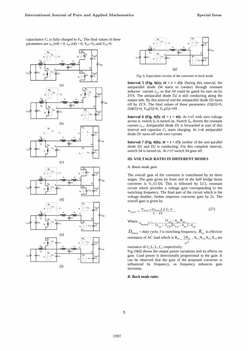
Fig. 6. Equivalent circuits of the converter in buck mode
Interval 5 (Fig. 6(e); t4 < t < t5): During this interval, the antiparallel diode D4 starts to conduct through resonant
inductor current iLr2 so that S4 could be gated for turn on by
ZVS. The antiparallel diode D2 is still conducting along the
output side. By this interval end the antiparallel diode D2 turns
off by ZCS. The final values of these parameters iS3(t5)=0,
iS4(t5)=0, VS4(t5)=0, VS3(t5)=VH .
Interval 6 (Fig. 6(f); t5 < t < t6): At t=t5 with zero voltage across it, switch S4 is turned on. Switch S4, diverts the resonant
current iLr2. Antiparallel diode D1 is forwarded at start of this
interval and capacitor C5 starts charging. At t=t6 antiparallel
diode D1 turns off with zero current.
Interval 7 (Fig. 6(h); t6 < t < t7): neither of the anti-parallel
diode D1 and D2 is conducting. For this complete interval,
switch S4 is turned on. At t=t7 switch S4 goes off.
III. VOLTAGE RATIO IN DIFFERENT MODES
A. Boost mode gain
The overall gain of the converter is contributed by its three
stages. The gain given by front end of the half bridge boost
converter is VL/(1-D). This is followed by LCL resonant
circuit which provides a voltage gain corresponding to the
switching frequency. The final part of the circuit which is the
voltage doubler, further improves converter gain by 2x. The
overall gain is given by
.
1
2
D
fGVV boostLow
High
(27)
Where
ac
Rac
RL
XCP
XL
X
acR
acR
LX
fboost
G
21
1
boostD = duty cycle, f is switching frequency, acR is effective
resistance of AC load which is Rac
2
2
dcR
, XCr,XL2,XL2,Xc2 are
reactance of Cr,L1,L1,C2 respectively.
Fig.10(d) shows the output power variations and its effects on
gain. Load power is directionally proportional to the gain. It
can be observed that the gain of the proposed converter is influenced by frequency, as frequency enhances gain
increases.
B. Buck mode ratio:
International Journal of Pure and Applied Mathematics Special Issue
1997

6
Only half the voltage VH is applied to the resonant component
on account of voltage divider circuit. The overall step down
ratio can be expressed as
)(5.0 fBuck
GBuck
DHigh
VLowV (28)
Where
1112121 LX
CPX
LX
CX
LX
LX
CPX
CX
CPX
LX
acbR
CPX
fbuck
G
Fig. 8(a) illustrates the gain g dependency of load . The buck ratio for higher load is much less as compared to that at a
lower load. Fig. 8(b) illustrates the relation between overall
ratios in buck mode when switching frequency is varied. It can
be seen that step down ratio is dependent on switching
frequency as frequency goes up, step down ratio increases.
IV. DESIGN OF THE CONVERTER
The design methodology for the converter by means of an
example for the following specifications is discussed here:
VLow=48V, VHigh=380V, output power, PO=350W. The
following are the assumptions made:
(a) Converter efficiency is presumed as 100%.
(b) Voltage ripples across capacitor C5, C6, C7 and C8 to be
very insignificant or minute.
(c) All the components are ideal and lossless. To decide the
component ratings, the design equations are derived. 1) Average current through input inductor is given by
(29)
2) At input voltage duty ratio is selected , i.e., VL = 48V
and full load based on maximum switch voltage rating.
(30)
3) Value of input boost inductor is given by
(31)
Where, is the boost inductor ripple current. For,
=2A, LB=159.77μH.
4) Sufficient energy difference stored in inductor L and LB is
supposed to be maintained to achieve ZVS of lower switch S2
and charge the capacitance CS1 and discharge Cs2 is given by
(32)
To ensure ZVS turn on of switch S1 the energy stored in
resonant inductor L1 at t=t1 has to be greater than energy stored in device capacitances of S1 and S2 and is given by
(33)
Parameters Values
Low side voltage Vlow 48V
High side voltage Vhigh 380V
Rated power Po 350W
Switching frequency fs
for boost operation
105 kHz
Switches, S1-S4 FCH041N60F, 600V,
76A MOSFET, Rdson = 36
mΩ
LB CM610125 MPP core, 17
turns, measured
value=160μH
L1 and L2 PC47RM14Z-12, RM
core, 12 turns, measured inductance = 30μH
C1 and C2 100μF high frequency
film capacitor,
Cr 0.1μF high frequency film
capacitor,
C3 and C4 30μF high frequency film
capacitor, 400V
Co 330μF Electrolytic
capacitor
DSP Texas Instrument
TMS320F28035
Table 1 Converter Specifications
In order to ensure ZVS for switch S3, the energy stored in
resonant inductor L2 at t=t1 has to be greater than energy
stored in device capacitances of S3 and S4 and is given by
(34)
Similarly, for S4 ZVS condition is energy stored in resonant
inductor L2 at t=t4 has to be greater than energy stored in
device capacitance of switch S3 and S4 and is given by
(35)
The resonant frequency of the LCL is given by
(36)
For resonant frequency of 91.93 kHz the C1=C2=100μF,
L=L1=L2=30μH and Cr=0.1μF.
V. PROTOTYPE RESULTS
The designed converter rated at 350W was simulated to test
verify the steady-state operation, analysis and design of the
proposed converter. Table I shows the specifications. For both
buck and boost operation, it was tested with Vlow = 48V and
Vhigh =380V at full load (350W). Experimental results for
boost operation are shown in Fig. 7. Fig. 7(b) confirms the ZVS turn on of switch S1 since anti-parallel diode DS1 is
conducting causing zero voltage across S1 before gating signal
is applied. In waveforms shown in Fig. 7(d) the input and
output current reads 0.7A and 8.4A. In Fig. 7(c) it can be seen
that antiparallel diode D3 and D4 conduct and commutate with
zero current. Therefore, reverse recovery losses are not
present. Fig. 7(e) shows that input voltage 48V is stepped-up
to 380V with small voltage ripple in the output voltage; boost
inductor ripple current is also small.
Boost operation:
International Journal of Pure and Applied Mathematics Special Issue
1998

7
(a)
(b)
(c)
(d)
(e)
Fig 7:(a)Current through L1 & L2, Voltage across Cr (b)ZVS
turn on of S1 (c)Current and Voltage across D2,D3 (d)Output
and input current waveforms (e) Step up voltage from 48V
and 380V
Buck operation:
(a)
(b)
(c)
(d)
(e)
Fig 8:(a) Current and voltage through D2 (b):Current through L,L1,L2 (c)ZVS turn-ON of switch S3 (d) ZVS turn-ON of switch S4 (e)Voltage and Current of S3.
The experimental results for buck operation are shown in Fig.8. Fig. 8(c) shows the gating signals for switch S3, it can
be seen that antiparallel diode conducts before the gating
signal is applied causing ZVS turn-on of the switch S3.
Similarly, ZVS turn-on of switch S4 is observed in Fig.8 (d).
In Fig. 8(a) anti-parallel diode D2 commutates with zero
current. Therefore, reverse recovery losses are insignificant in
this case. It can be observed that the experimental waveforms
coincide with analytically predicted steady-state operating
waveforms. The converter maintains soft-switching under
varying load conditions.
VI. CONCLUSIONS
In this paper, transformer-less LCL resonant soft-switching
bidirectional dc/dc converter is proposed. High step up/step
down ratio, high efficiency, low device voltage stress, ZVS
turn-on for all switches and ZCS turn-on and turn-off for all
International Journal of Pure and Applied Mathematics Special Issue
1999

8
diodes in both buck/boost mode of operation were the key
features of this prototype. For the wide load range, the
suggested converter can achieve ZVS for switches and ZCS
for diodes. Without the external snubber circuit, the device
voltage is maintained. Simulation results have been
manifested to verify the suggested analysis, design and soft-switching, and to validate the performance of the converter.
The converter maintains high efficiency for both the direction
of power flow.
REFERENCES
[1] Lasseter, R.H. and Paigi, P.,"Microgrid: a conceptual solution," IEEE
Power Electronics Specialists Conference, vol.6, pp.4285-4290, June 2004.
[2] Ito, Y., Zhongqing, Y., Akagi, H., "DC microgrid based distribution power
generation system," IEEE Power Electronics and Motion Control Conference,
vol.3,pp.1740-1745,Aug. 2004.
[3] Gerber, M., Ferreira, J.A, Seliger, N. and Hofsajer, I.W.,"Design and
evaluation of an automotive integrated system module," IEEE Industry
Applications Conference, vol.2, pp.1144-1151,Oct. 2005.
[4] H.-L. Do "Non-isolated bidirectional zero-voltage-switching DC-DC
converter", IEEE Trans. Power Electron., vol. 26, no. 9, pp.2563 -2569 2011.
[5] D. Zhang, D. Y. Chen, and F. C. Lee, “An experimental comparison of
conducted EMI emissions between a zero-voltage transition circuit and a hard
switching circuit,” in Proc. IEEE Power Electron. Spec. Conf., pp. 1992–
1997, 1996.
[6] W. Li, X. Lv, Y. Deng, J. Liu, and X. He, “A review of non-isolated high
step-up DC/DC converters in renewable energy applications,” in Proc.24th
Annu. IEEE Appl. Power Electron. Conf. Expo., pp. 364–369, 2009.
[7] X. Li and A. K. S. Bhat "Analysis and design of high-frequency isolated
dual-bridge series resonant DC/DC converter", IEEE Trans. Power Electron.,
vol. 25, no. 4, pp.850 -862 2010.
[8] S. Han and D. Divan "Bi-directional DC/DC converters for plug-in hybrid
electric vehicle (PHEV) applications", Proc. IEEE 23rd Annu. Appl. Power
Electron. Conf. Expo., pp.784 -789 2008.
[9] Pan Xuewei and Rathore, AK., "Novel Bidirectional Snubberless
Naturally Commutated Soft-Switching Current-Fed Full Bridge Isolated
DC/DC Converter for Fuel Cell Vehicles," IEEE Transactions on Industrial
Electronics, vol.61, no.5, pp.2307,2315, May 2014.
[10] T.K.Sethuramalingam and B.Nagaraj, “A Comparative Approach On Pid
Controller Tuning Using Soft Computingtechniques”, International Journal of
Innovations in Scientific and Engineering Research
(IJISER),vol.1,No.12,pp.460-465,DEC 2014.
[11] R. J. Wai and R. Y. Duan "High-efficiency bidirectional converter for
power sources with great voltage diversity", IEEE Trans. Power. Electron. ,
vol. 22, no. 5, pp. 1986 -1996 2007.
[12] Das, P. and Moschopoulos, G., "Analysis and Design of a Non-Isolated
Bidirectional ZVS-PWM Active Clamped DC-DC Converter," IEEE Applied
Power Electronics Conference and Exposition, pp.1452-1458, Feb. 2009.
[13] Lei Jiang Mi, C.C. Siqi Li et. al. "A Novel Soft-Switching Bidirectional
DC–DC Converter With Coupled Inductors," IEEE Trans. on Industry Appl.,
vol.49, no.6, pp.2730-2740, Dec. 2013.
[14] Kwon, Minho et. al.,"High Gain Soft-Switching Bidirectional DC–DC
Converter for Eco-Friendly Vehicles.", IEEE Trans. on Power Electron. Vol.
29, no. 4, pp.1659-1666, 2014.
[15] L. S. Yang and T. J. Liang "Analysis and implementation of a novel
bidirectional DC-DC converter", IEEE Trans. on Ind. Electron., vol. 59, no.
1,pp.422-434 2012.
[16] Yi-Ping Hsieh et. al. "High-Conversion-Ratio Bidirectional DC–DC
Converter With Coupled Inductor,", IEEE Transactions on Industrial
Electronics, vol.61, no.1, pp.210,222, Jan. 2014.
[17] R. J. Wai, R. Y. Duan and K. H. Jheng "High-efficiency bidirectional dc-
dc converter with high-voltage gain", IET Power Electron., vol. 5, no. 2,
pp.173 -184.2012.
International Journal of Pure and Applied Mathematics Special Issue
2000

2001

2002