radiation tolerant sensors for pixel detectors michael moll cern - geneva - switzerland pixel 2005...
Post on 22-Dec-2015
219 views
TRANSCRIPT
Radiation Tolerant Sensorsfor Pixel Detectors
Michael MollMichael Moll
CERN - Geneva - SwitzerlandCERN - Geneva - Switzerland
PIXEL 2005 international workshop, September 5-8, Bonn, Germany
on behalf of the
- CERN-RD50 project –
http://www.cern.ch/rd50http://www.cern.ch/rd50

Michael Moll – PIXEL 2005, September 7, 2005 -2-
RD50 Outline
Motivation to develop radiation harder detectors: Super-LHC
Introduction to the RD50 collaboration
Radiation Damage in Silicon Detectors (A review in 5 slides) Macroscopic damage (changes in detector properties)
Approaches to obtain radiation hard sensors Material Engineering Device Engineering
Summary

Michael Moll – PIXEL 2005, September 7, 2005 -3-
RD50 Main motivations for R&D on Radiation Tolerant Detectors: Super - LHC
• LHC upgrade LHC (2007), L = 1034cm-2s-1
(r=4cm) ~ 3·1015cm-2
Super-LHC (2015 ?), L = 1035cm-2s-1
(r=4cm) ~ 1.6·1016cm-2
• LHC (Replacement of components) e.g. - LHCb Velo detectors (~2010) - ATLAS Pixel B-layer (~2012)
• Linear collider experiments (generic R&D)Deep understanding of radiation damage will be fruitful for linear collider experiments where high doses of e, will play a significant role.
5 years
2500 fb-1
10 years
500 fb-1
5
0 10 20 30 40 50 60
r [cm]
1013
5
1014
5
1015
5
1016
eq
[cm
-2]
total fluence eqtotal fluence eq
neutrons eq
pions eq
other charged
SUPER - LHC (5 years, 2500 fb-1)
hadrons eqATLAS SCT - barrelATLAS Pixel
Pixel (?) Ministrip (?)
Macropixel (?)
(microstrip detectors)
[M.Moll, simplified, scaled from ATLAS TDR]

Michael Moll – PIXEL 2005, September 7, 2005 -4-
RD50 The CERN RD50 Collaboration http://www.cern.ch/rd50
Collaboration formed in November 2001 Experiment approved as RD50 by CERN in June 2002 Main objective:
Presently 251 members from 51 institutes
Development of ultra-radiation hard semiconductor detectors for the luminosity upgrade of the LHC to 1035 cm-2s-1 (“Super-LHC”).
Challenges: - Radiation hardness up to 1016 cm-2 required - Fast signal collection (Going from 25ns to 10 ns bunch crossing ?)
- Low mass (reducing multiple scattering close to interaction point)- Cost effectiveness (big surfaces have to be covered with detectors!)
RD50: Development of Radiation Hard Semiconductor Devices for High Luminosity Colliders
Belarus (Minsk), Belgium (Louvain), Canada (Montreal), Czech Republic (Prague (3x)), Finland (Helsinki, Lappeenranta), Germany (Berlin, Dortmund, Erfurt, Freiburg, Hamburg, Karlsruhe), Israel (Tel Aviv), Italy
(Bari, Bologna, Florence, Padova, Perugia, Pisa, Trento, Turin), Lithuania (Vilnius), Norway (Oslo (2x)), Poland (Warsaw(2x)), Romania (Bucharest (2x)), Russia (Moscow), St.Petersburg), Slovenia (Ljubljana), Spain
(Barcelona, Valencia), Switzerland (CERN, PSI), Ukraine (Kiev), United Kingdom (Exeter, Glasgow, Lancaster, Liverpool, Sheffield, University of Surrey), USA (Fermilab, Purdue University,
Rochester University, SCIPP Santa Cruz, Syracuse University, BNL, University of New Mexico)

Michael Moll – PIXEL 2005, September 7, 2005 -5-
RD50 Radiation Damage in Silicon Sensors
Two general types of radiation damage to the detector materials:
Bulk (Crystal) damage due to Non Ionizing Energy Loss (NIEL) - displacement damage, built up of crystal defects –
I. Change of effective doping concentration (higher depletion voltage, under- depletion)
II. Increase of leakage current (increase of shot noise, thermal runaway)
III. Increase of charge carrier trapping (loss of charge)
Surface damage due to Ionizing Energy Loss (IEL) - accumulation of positive in the oxide (SiO2) and the Si/SiO2 interface – affects: interstrip capacitance (noise factor), breakdown behavior, …
Impact on detector performance and Charge Collection Efficiency (depending on detector type and geometry and readout electronics!)
Signal/noise ratio is the quantity to watch Sensors can fail from radiation damage !
A reviewin 5 slides
Michael Moll – PIXEL 2005, September 7, 2005 -6-
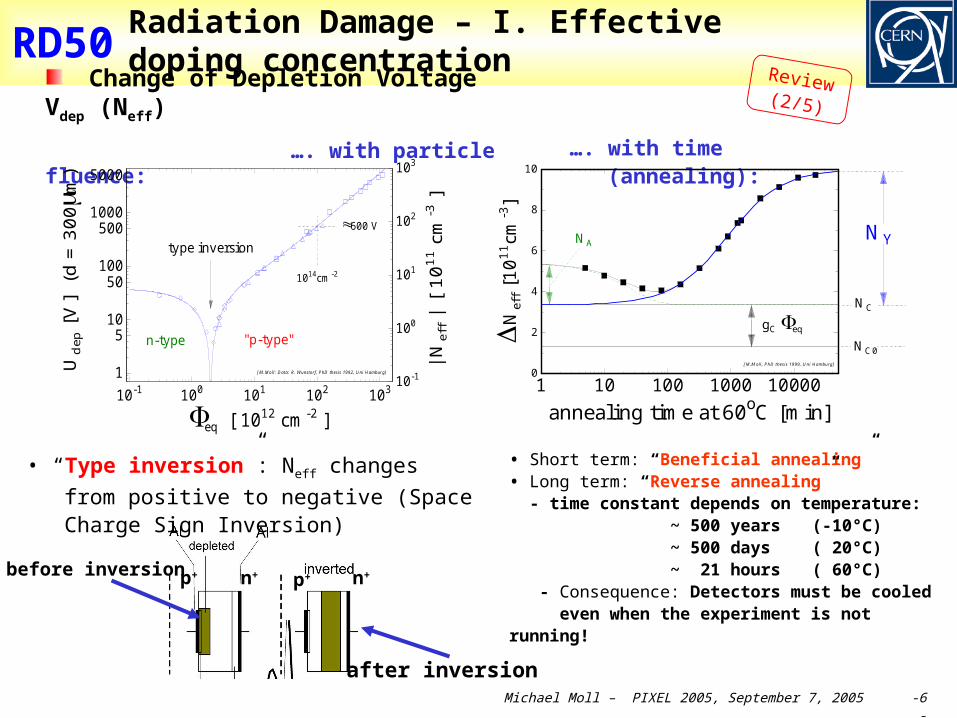
RD50Radiation Damage – I. Effective doping concentration
Change of Depletion Voltage Vdep (Neff)
…. with particle fluence:
before inversion
after inversion
n+ p+ n+
• “Type inversion”: Neff changes from positive to
negative (Space Charge Sign Inversion)
10-1 100 101 102 103
eq [ 1012 cm-2 ]
1
510
50100
5001000
5000
Ude
p [V
] (
d =
300
m)
10-1
100
101
102
103
| Nef
f | [
1011
cm
-3 ]
600 V
1014cm-2
type inversion
n-type "p-type"
[M.Moll: Data: R. Wunstorf, PhD thesis 1992, Uni Hamburg]
• Short term: “Beneficial annealing” • Long term: “Reverse annealing” - time constant depends on temperature: ~ 500 years (-10°C) ~ 500 days ( 20°C) ~ 21 hours ( 60°C) - Consequence: Detectors must be cooled even when the experiment is not running!
…. with time (annealing):
NC
NC0
gC eq
NYNA
1 10 100 1000 10000annealing time at 60oC [min]
0
2
4
6
8
10
N
eff [
1011
cm-3
]
[M.Moll, PhD thesis 1999, Uni Hamburg]
p+
Review(2/5)

Michael Moll – PIXEL 2005, September 7, 2005 -7-
RD50 Radiation Damage – II. Leakage Current
1011 1012 1013 1014 1015
eq [cm-2]
10-6
10-5
10-4
10-3
10-2
10-1
I /
V
[A/c
m3 ]
n-type FZ - 7 to 25 Kcmn-type FZ - 7 Kcmn-type FZ - 4 Kcmn-type FZ - 3 Kcm
n-type FZ - 780 cmn-type FZ - 410 cmn-type FZ - 130 cmn-type FZ - 110 cmn-type CZ - 140 cm
p-type EPI - 2 and 4 Kcm
p-type EPI - 380 cm
[M.Moll PhD Thesis][M.Moll PhD Thesis]
Damage parameter (slope in figure)
Leakage current per unit volume and particle fluence
is constant over several orders of fluenceand independent of impurity concentration in Si can be used for fluence measurement
eqV
I
α
80 min 60C
Change of Leakage Current (after hadron irradiation)
…. with particle fluence:
Leakage current decreasing in time (depending on temperature)
Strong temperature dependence
Consequence: Cool detectors during operation! Example: I(-10°C) ~1/16 I(20°C)
1 10 100 1000 10000annealing time at 60oC [minutes]
0
1
2
3
4
5
6
(t)
[10
-17 A
/cm
]
1
2
3
4
5
6
oxygen enriched silicon [O] = 2.1017 cm-3
parameterisation for standard silicon [M.Moll PhD Thesis]
80 min 60C
…. with time (annealing):
Tk
EI
B
g
2exp
Review(3/5)

Michael Moll – PIXEL 2005, September 7, 2005 -8-
RD50
Deterioration of Charge Collection Efficiency (CCE) by trapping
tQtQ
heeffhehe
,,0,
1exp)(
0 2.1014 4.1014 6.1014 8.1014 1015
particle fluence - eq [cm-2]
0
0.1
0.2
0.3
0.4
0.5
Inve
rse
trap
ping
tim
e 1
/ [n
s-1]
data for electronsdata for electronsdata for holesdata for holes
24 GeV/c proton irradiation24 GeV/c proton irradiation
[M.Moll; Data: O.Krasel, PhD thesis 2004, Uni Dortmund][M.Moll; Data: O.Krasel, PhD thesis 2004, Uni Dortmund]
Increase of inverse trapping time (1/) with fluence
Trapping is characterized by an effective trapping time eff for electrons and holes:
….. and change with time (annealing):
5 101 5 102 5 103
annealing time at 60oC [min]
0.1
0.15
0.2
0.25
Inve
rse
trap
ping
tim
e 1
/ [n
s-1]
data for holesdata for holesdata for electronsdata for electrons
24 GeV/c proton irradiation24 GeV/c proton irradiationeq = 4.5.1014 cm-2 eq = 4.5.1014 cm-2
[M.Moll; Data: O.Krasel, PhD thesis 2004, Uni Dortmund][M.Moll; Data: O.Krasel, PhD thesis 2004, Uni Dortmund]
where defectsheeff
N,
1
Radiation Damage – III. Trapping Review(4/5)

Michael Moll – PIXEL 2005, September 7, 2005 -9-
RD50 Impact on Detector: Decrease of CCE - Loss of signal and increase of noise -
Two basic mechanisms reduce collectable charge: trapping of electrons and holes (depending on drift and shaping time !) under-depletion (depending on detector design and geometry !)
Example: ATLAS microstrip detectors + fast electronics (25ns)
n-in-n versus p-in-n - same material, ~ same fluence- over-depletion needed
0 100 200 300 400 500 600
bias [volts]
0.20
0.40
0.60
0.80
1.00
CC
E (
arb.
uni
ts)
n-in-n (7.1014 23 GeV p/cm2)
n-in-n
p-in-n (6.1014 23 GeV p/cm2)
p-in-n
Laser (1064nm) measurements
[M.Moll: Data: P.Allport et al. NIMA 513 (2003) 84]
p-in-n : oxygenated versus standard FZ- beta source- 20% charge loss after 5x10¹⁴ p/cm2 (23 GeV)
0 1 2 3 4 5p [1014 cm-2]
0
20
40
60
80
100
Q/Q
0 [%
]
oxygenatedstandard
max collected charge (overdepletion)
collected at depletion voltage
M.Moll [Data: P.Allport et all, NIMA 501 (2003) 146]
Review(5/5)

Michael Moll – PIXEL 2005, September 7, 2005 -10-
RD50 Approaches to develop radiation harder tracking detectors
Defect Engineering of Silicon Understanding radiation damage
• Macroscopic effects and Microscopic defects• Simulation of defect properties & kinetics• Irradiation with different particles & energies
Oxygen rich Silicon• DOFZ, Cz, MCZ, EPI
Oxygen dimer & hydrogen enriched Si Pre-irradiated Si Influence of processing technology
New Materials Silicon Carbide (SiC), Gallium Nitride (GaN) Diamond: CERN RD42 Collaboration Amorphous silicon
Device Engineering (New Detector Designs) p-type silicon detectors (n-in-p) thin detectors 3D and Semi 3D detectors Stripixels Cost effective detectors Simulation of highly irradiated detectors Monolithic devices
Scientific strategies:
I. Material engineering
II. Device engineering
III. Change of detectoroperational conditions
CERN-RD39“Cryogenic Tracking Detectors”
Talks this WorkshopH.Kagan, R.Stone
D.Moraes S.Parker
M.Swartz

Michael Moll – PIXEL 2005, September 7, 2005 -11-
RD50 Outline
Motivation to develop radiation harder detectors: Super-LHC
Introduction to the RD50 collaboration
Radiation Damage in Silicon Detectors (A review in 4 slides) Macroscopic damage (changes in detector properties)
Approaches to obtain radiation hard sensors
Material Engineering Device Engineering
Summary

Michael Moll – PIXEL 2005, September 7, 2005 -12-
RD50
Property Diamond GaN 4H SiC Si Eg [eV] 5.5 3.39 3.26 1.12 Ebreakdown [V/cm] 107 4·106 2.2·106 3·105 e [cm2/Vs] 1800 1000 800 1450 h [cm2/Vs] 1200 30 115 450 vsat [cm/s] 2.2·107 - 2·107 0.8·107 Z 6 31/7 14/6 14 r 5.7 9.6 9.7 11.9 e-h energy [eV] 13 8.9 7.6-8.4 3.6 Density [g/cm3] 3.515 6.15 3.22 2.33 Displacem. [eV] 43 15 25 13-20
Sensor Materials
Wide bandgap (3.3eV) lower leakage current
than silicon
Signal:Diamond 36 e/mSiC 51 e/mSi 89 e/m
more charge than diamond
Higher displacement threshold than silicon
radiation harder than silicon (?)
R&D on diamond detectors:RD42 – Collaboration
http://cern.ch/rd42/
Recent review: P.J.Sellin and J.Vaitkus on behalf of RD50 “New materials for radiation hard semiconductor detectors”, submitted to NIMA

Michael Moll – PIXEL 2005, September 7, 2005 -13-
RD50 SiC: CCE after irradiation
CCE before irradiation 100 % with particles and MIPS tested on various samples 20-40m
CCE after irradiation with particles neutron irradiated samples material produced by CREE 25 m thick layer
[S.Sciortino et al., presented on the RESMDD 04 conference, in press with NIMA ]
20% CCE (α) after 7x10¹⁵ n/cm2!
35% CCE() (CCD ~6m ; ~ 300 e) after 1.4x10¹⁶ p/cm2
much less than in silicon (see later)
Michael Moll – PIXEL 2005, September 7, 2005 -14-
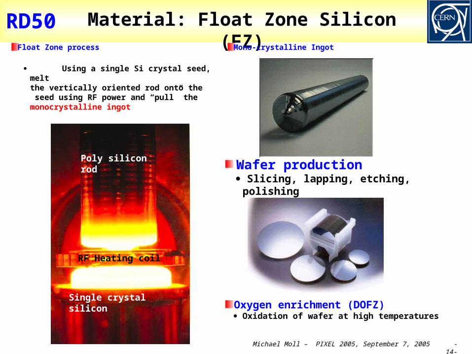
RD50 Material: Float Zone Silicon (FZ)
Using a single Si crystal seed, meltthe vertically oriented rod onto the seed using RF power and “pull” themonocrystalline ingot
Wafer production Slicing, lapping, etching, polishing
Mono-crystalline Ingot
Single crystal silicon
Poly silicon rod
RF Heating coil
Float Zone process
Oxygen enrichment (DOFZ) Oxidation of wafer at high temperatures

Michael Moll – PIXEL 2005, September 7, 2005 -15-
RD50 Czochralski silicon (Cz) & Epitaxial silicon (EPI)
Pull Si-crystal from a Si-melt contained in a silica crucible while rotating.
Silica crucible is dissolving oxygen into the melt high concentration of O in CZ
Material used by IC industry (cheap) Recent developments (~2 years) made CZ
available in sufficiently high purity (resistivity) to allow for use as particle detector.
Czochralski Growth
Czochralski silicon
Epitaxial silicon
Chemical-Vapor Deposition (CVD) of Silicon CZ silicon substrate used in-diffusion of oxygen growth rate about 1m/min excellent homogeneity of resistivity up to 150 m thick layers produced (thicker is possible) price depending on thickness of epi-layer but not
extending ~ 3 x price of FZ wafer

Michael Moll – PIXEL 2005, September 7, 2005 -16-
RD50 Oxygen concentration in FZ, CZ and EPI
0 10 20 30 40 50 60 70 80 90 100Depth [m]
51016
51017
51018
5
O-c
once
ntra
tion
[1/c
m3 ]
SIMS 25 m SIMS 25 m
25 m
u25
mu
SIMS 50 mSIMS 50 m
50 m
u50
mu
SIMS 75 mSIMS 75 m
75 m
u75
mu
simulation 25 msimulation 25 msimulation 50 msimulation 50 msimulation 75msimulation 75m
Cz and DOFZ silicon Epitaxial silicon
EPI: Oi and O2i (?) diffusion from substrate into epi-layer during production
EPI: in-homogeneous oxygen distribution
CZ: high Oi (oxygen) and O2i (oxygen dimer) concentration (homogeneous)
CZ: formation of Thermal Donors possible !
0 50 100 150 200 250depth [m]
51016
51017
51018
5
O-c
once
ntra
tion
[cm
-3]
51016
51017
51018
5
Cz as grown
DOFZ 72h/1150oCDOFZ 48h/1150oCDOFZ 24h/1150oC [G.Lindstroem et al.]
[G.Lindström et al.,10th European Symposium on Semiconductor Detectors, 12-16 June 2005]
DOFZ: inhomogeneous oxygen distribution DOFZ: oxygen content increasing with time
at high temperature
EPIlayer CZ substrate

Michael Moll – PIXEL 2005, September 7, 2005 -17-
RD50 Standard FZ, DOFZ, Cz and MCz Silicon
24 GeV/c proton irradiation
0 2 4 6 8 10proton fluence [1014 cm-2]
0
200
400
600
800
Vde
p [V
]0
2
4
6
8
10
12
Nef
f [10
12 c
m-3
]
CZ <100>, TD killedCZ <100>, TD killedMCZ <100>, HelsinkiMCZ <100>, HelsinkiSTFZ <111>STFZ <111>DOFZ <111>, 72 h 11500CDOFZ <111>, 72 h 11500C Standard FZ silicon
• type inversion at ~ 21013 p/cm2
• strong Neff increase at high fluence
Oxygenated FZ (DOFZ)• type inversion at ~ 21013 p/cm2
• reduced Neff increase at high fluence
CZ silicon and MCZ silicon no type inversion in the overall fluence range (verified by TCT measurements)
(verified for CZ silicon by TCT measurements, preliminary result for MCZ silicon) donor generation overcompensates acceptor generation in high fluence range
Common to all materials (after hadron irradiation): reverse current increase increase of trapping (electrons and holes) within ~ 20%

Michael Moll – PIXEL 2005, September 7, 2005 -18-
RD50
0 2.1015 4.1015 6.1015 8.1015 1016
eq [cm-2]
0
5.1013
1014
Nef
f (t 0
) [c
m-3
]
0
50
100
150
Vfd
(t 0
)[V
] no
rmal
ized
to 5
0 m
50 m50 m
25 m25 m
Reactor neutronsReactor neutrons
Ta = 80oCTa = 80oC
Epitaxial silicon grown by ITME Layer thickness: 25, 50, 75 m; resistivity: ~ 50 cm Oxygen: [O] 91016cm-3; Oxygen dimers (detected via IO2-defect formation)
EPI Devices – Irradiation experiments
No type inversion in the full range up to ~ 1016 p/cm2 and ~ 1016 n/cm2 (type inversion only observed during long term annealing)
Proposed explanation: introduction of shallow donors bigger than generation of deep acceptors
G.Lindström et al.,10th European Symposium on Semiconductor Detectors, 12-16 June 2005
0 2.1015 4.1015 6.1015 8.1015 1016
eq [cm-2]
0
1014
2.1014
Nef
f(t0)
[cm
-3]
25 m, 80 oC25 m, 80 oC
50 m, 80 oC50 m, 80 oC
75 m, 80 oC75 m, 80 oC
23 GeV protons23 GeV protons
320V (75m)
105V (25m)
230V (50m)
Michael Moll – PIXEL 2005, September 7, 2005 -19-
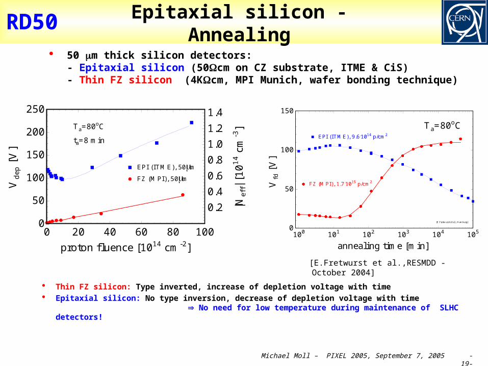
RD50 Epitaxial silicon - Annealing
50 m thick silicon detectors:- Epitaxial silicon (50cm on CZ substrate, ITME & CiS) - Thin FZ silicon (4Kcm, MPI Munich, wafer bonding technique)
Thin FZ silicon: Type inverted, increase of depletion voltage with time Epitaxial silicon: No type inversion, decrease of depletion voltage with time
No need for low temperature during maintenance of SLHC detectors!
[E.Fretwurst et al.,RESMDD - October 2004]
100 101 102 103 104 105
annealing time [min]
0
50
100
150
Vfd
[V
]
EPI (ITME), 9.6.1014 p/cm2EPI (ITME), 9.6.1014 p/cm2
FZ (MPI), 1.7.1015 p/cm2FZ (MPI), 1.7.1015 p/cm2
Ta=80oCTa=80oC
[E.Fretwurst et al., Hamburg][E.Fretwurst et al., Hamburg]
0 20 40 60 80 100proton fluence [1014 cm-2]
0
50
100
150
200
250
Vde
p [V
]
0.20.40.60.81.01.21.4
|Nef
f| [1
014 c
m-3
]
EPI (ITME), 50mEPI (ITME), 50m
FZ (MPI), 50mFZ (MPI), 50m
Ta=80oCTa=80oC
ta=8 minta=8 min
Michael Moll – PIXEL 2005, September 7, 2005 -20-
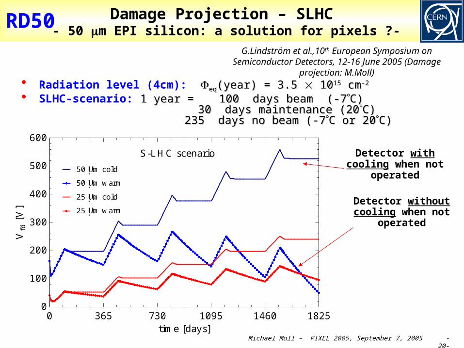
RD50 Damage Projection – SLHC - 50 m EPI silicon: a solution for pixels ?-
Radiation level (4cm): eqeq(year) = 3.5 (year) = 3.5 10 101515 cm cm-2 -2
SLHC-scenario: 1 year = 1 year = 100 days beam (-7100 days beam (-7C)C) 30 days maintenance (20 30 days maintenance (20C)C)
235 days no beam (-7235 days no beam (-7C or 20C or 20C)C)
G.Lindström et al.,10th European Symposium on Semiconductor Detectors, 12-16 June 2005 (Damage projection: M.Moll)
Detector withcooling when not
operated
0 365 730 1095 1460 1825time [days]
0
100
200
300
400
500
600
Vfd
[V
]
50 m cold50 m cold
50 m warm50 m warm
25 m cold25 m cold
25 m warm25 m warm
S-LHC scenarioS-LHC scenario
Detector withoutcooling when not
operated
Michael Moll – PIXEL 2005, September 7, 2005 -21-
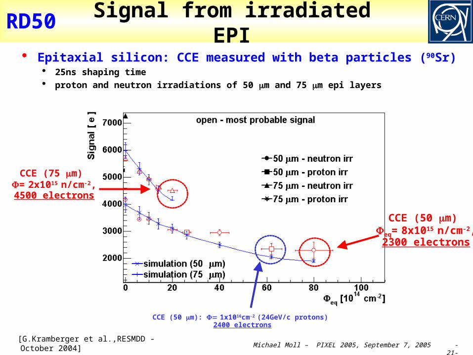
RD50 Signal from irradiated EPI
Epitaxial silicon: CCE measured with beta particles (90Sr) 25ns shaping time proton and neutron irradiations of 50 m and 75 m epi layers
CCE (50 m) eq= 8x10¹⁵ n/cm-2,
2300 electrons
CCE (50 m): 1x1016cm-2 (24GeV/c protons) 2400 electrons
CCE (75 m) = 2x10¹⁵ n/cm-2,4500 electrons
[G.Kramberger et al.,RESMDD - October 2004]

Michael Moll – PIXEL 2005, September 7, 2005 -22-
RD50 Microscopic defects
I
I
V
V
Distribution of vacancies created by a 50 keV Si-ion
in silicon (typical recoil energy for 1 MeV neutrons):
Schematic[Van Lint 1980]
Simulation[M.Huhtinen 2001]
Defects can be electrically active (levels in the band gap) - capture and release electrons and holes from conduction and valence band
can be charged - can be generation/recombination centers - can be trapping centers
Vacancy + Interstitial
“point defects”, mobile in silicon,can react with impurities (O,C,..)
V
I
point defects and clusters of defects
particle SiS EK>25 eV
EK > 5 keV
Damage to the silicon crystal: Displacement of lattice atoms
80 nm

Michael Moll – PIXEL 2005, September 7, 2005 -23-
RD50 Characterization of microscopic defects - and proton irradiated silicon detectors -
2003: Major breakthrough on -irradiated samples For the first time macroscopic changes of the depletion voltage and leakage current
can be explained by electrical properties of measured defects !
2004: Big step in understanding the improved radiation tolerance of oxygen enriched and epitaxial silicon after proton irradiation
[APL, 82, 2169, March 2003]
Almost independent of oxygen content: Donor removal “Cluster damage” negative charge
Influenced by initial oxygen content: I–defect: deep acceptor level at EC-0.54eV (good candidate for the V2O defect) negative charge
Influenced by initial oxygen dimer content (?): BD-defect: bistable shallow thermal donor (formed via oxygen dimers O2i) positive charge
Levels responsible for depletion voltage changes after proton irradiation:
D-defectI-defect
[I.Pintilie, RESMDD, Oct.2004]
Michael Moll – PIXEL 2005, September 7, 2005 -24-
RD50 Outline
Motivation to develop radiation harder detectors: Super-LHC
Introduction to the RD50 collaboration
Radiation Damage in Silicon Detectors (A review in 4 slides) Macroscopic damage (changes in detector properties)
Approaches to obtain radiation hard sensors Material Engineering
Device Engineering
Summary

Michael Moll – PIXEL 2005, September 7, 2005 -25-
RD50
p-on-n silicon, under-depleted:
• Charge spread – degraded resolution
• Charge loss – reduced CCE
p+on-n
Device engineeringp-in-n versus n-in-n detectors
n-on-n silicon, under-depleted:
•Limited loss in CCE
•Less degradation with under-depletion
•Collect electrons (fast)
n+on-n
n-type silicon after type inversion:

Michael Moll – PIXEL 2005, September 7, 2005 -26-
RD50 n-in-p microstrip detectors
Miniature n-in-p microstrip detectors (280m) Detectors read-out with LHC speed (40MHz) chip (SCT128A) Material: standard p-type and oxygenated (DOFZ) p-type Irradiation:
At the highest fluence Q~6500e at Vbias=900V
G. Casse et al., NIMA535(2004) 362
CCE ~ 60% after 3 1015 p cm-2 at 900V( standard p-type)
0 2.1015 4.1015 6.1015 8.1015 1016
fluence [cm-2]
0
5
10
15
20
25
CC
E (
103 e
lect
rons
)
24 GeV/c proton irradiation24 GeV/c proton irradiation
[Data: G.Casse et al., Liverpool, February 2004][Data: G.Casse et al., Liverpool, February 2004]
CCE ~ 30% after 7.5 1015 p cm-2 900V (oxygenated p-type)
n-in-p: - no type inversion, high electric field stays on structured side - collection of electrons

Michael Moll – PIXEL 2005, September 7, 2005 -27-
RD50 Annealing of p-type sensors
p-type strip detector (280m) irradiated with 23 GeV p (7.5 1015 p/cm2 )
expected from previous CV measurement of Vdep:- before reverse annealing:
Vdep~ 2800V
- after reverse annealing
Vdep > 12000V
no reverse annealing visible in the CCE measurement !
G.Casse et al.,10th European Symposium on Semiconductor Detectors, 12-16 June 2005
0 100 200 300 400 500
time at 80oC[min]
0 500 1000 1500 2000 2500time [days at 20oC]
02468
101214161820
CC
E (
103 e
lect
rons
)
800 V800 V
1.1 x 1015cm-2 1.1 x 1015cm-2 500 V500 V
3.5 x 1015cm-2 (500 V)3.5 x 1015cm-2 (500 V)
7.5 x 1015cm-2 (700 V)7.5 x 1015cm-2 (700 V)
M.MollM.Moll
[Data: G.Casse et al., to be published in NIMA][Data: G.Casse et al., to be published in NIMA]
Michael Moll – PIXEL 2005, September 7, 2005 -28-
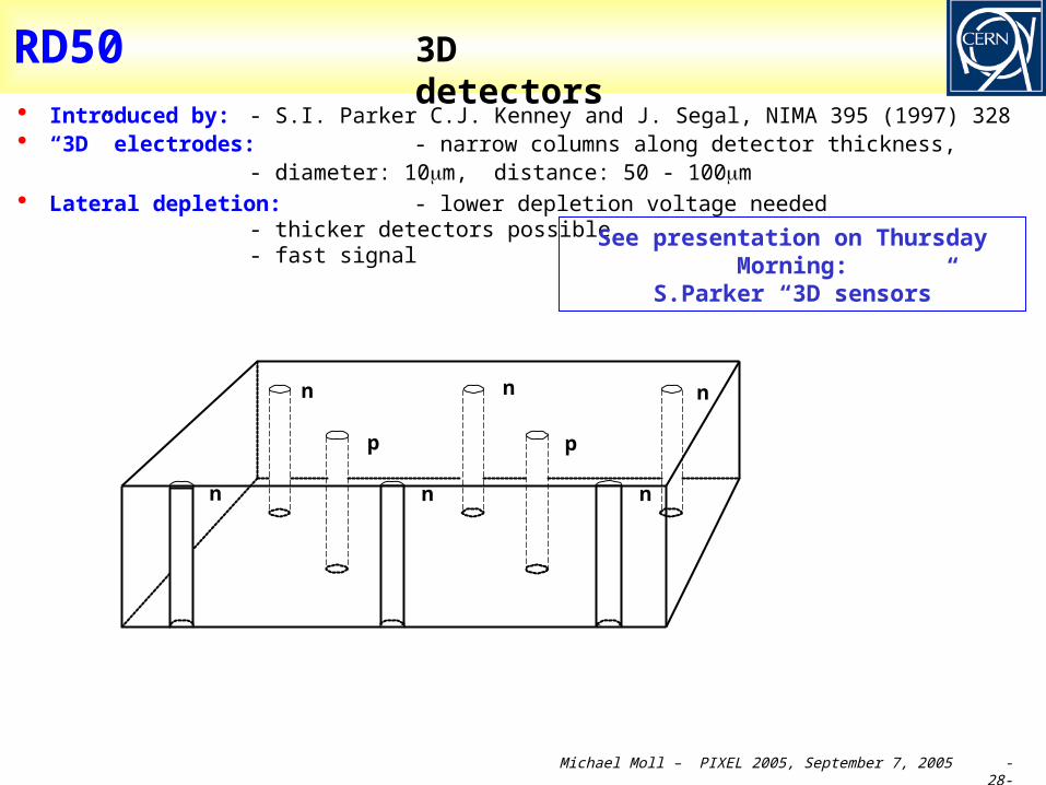
RD50 Introduced by: - S.I. Parker C.J. Kenney and J. Segal, NIMA 395 (1997) 328 “3D” electrodes: - narrow columns along detector thickness,
- diameter: 10m, distance: 50 - 100m Lateral depletion: - lower depletion voltage needed
- thicker detectors possible- fast signal
3D detectors
n
n
pp
n
n n
n
See presentation on Thursday Morning: S.Parker “3D sensors”

Michael Moll – PIXEL 2005, September 7, 2005 -29-
RD50 Introduced by: - S.I. Parker C.J. Kenney and J. Segal, NIMA 395 (1997) 328 “3D” electrodes: - narrow columns along detector thickness,
- diameter: 10m, distance: 50 - 100m Lateral depletion: - lower depletion voltage needed
- thicker detectors possible- fast signal
3D & Single Type Column 3D detectors
n
npp
n
n n
n
See presentation on Thursday Morning: S.Parker “3D sensors”
Simplified 3D architecture n+ columns in p-type substrate, p+ backplane operation similar to standard 3D detector
Simplified process hole etching and doping only done once
no wafer bonding technology needed [C. Piemonte et al., NIM A541 (2005) 441]
10ns
Simulation worst case shown (hit in middle of cell) still CCE below 10ns possible
Fabrication: under way IRST(Italy), CNM Barcelona
Michael Moll – PIXEL 2005, September 7, 2005 -30-
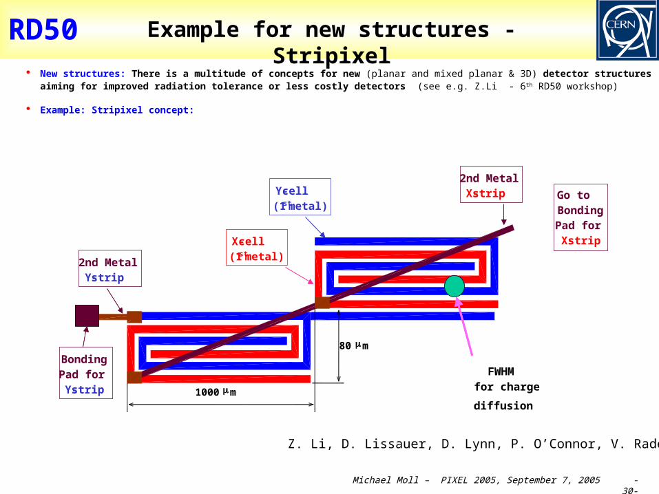
RD50 Example for new structures - Stripixel
1000 m
80 m
X-cell(1st metal)
Y-cell
(1st metal)
2nd MetalY-strip
2nd MetalX-strip
FWHM
for charge
diffusion
Bonding
Pad for
Y-strip
Go to
BondingPad for
X-strip
Z. Li, D. Lissauer, D. Lynn, P. O’Connor, V. Radeka
New structures: There is a multitude of concepts for new (planar and mixed planar & 3D) detector structures aiming for improved radiation tolerance or less costly detectors (see e.g. Z.Li - 6th RD50 workshop)
Example: Stripixel concept:

Michael Moll – PIXEL 2005, September 7, 2005 -31-
RD50 Summary At fluences up to 1015cm-2 (Outer layers of a SLHC detector) the change of depletion
voltage and the large area to be covered by detectors is the major problem. CZ silicon detectors could be a cost-effective radiation hard solution
(no type inversion, use p-in-n technology) p-type silicon microstrip detectors show very encouraging results:
CCE 6500 e; eq=
41015 cm-2, 300m, collection of electrons, no reverse annealing observed in CCE measurement!
At the fluence of 1016cm-2 (Innermost layer of a SLHC detector) the active thickness of any silicon material is significantly reduced due to trapping. The promising new options are: Thin/EPI detectors : drawback: radiation hard electronics for low signals needed e.g. 2300e at eq 8x1015cm-2, 50m EPI, …. thicker layers will be tested in 2005/2006 3D detectors : drawback: technology has to be optimized ….. steady progress within RD50
New Materials like SiC and GaN (not shown) have been characterized . CCE tests show that these materials are not radiation harder than silicon Further information: http://cern.ch/rd50/

Michael Moll – PIXEL 2005, September 7, 2005 -32-
RD50 Spares
Spare slides
Michael Moll – PIXEL 2005, September 7, 2005 -33-
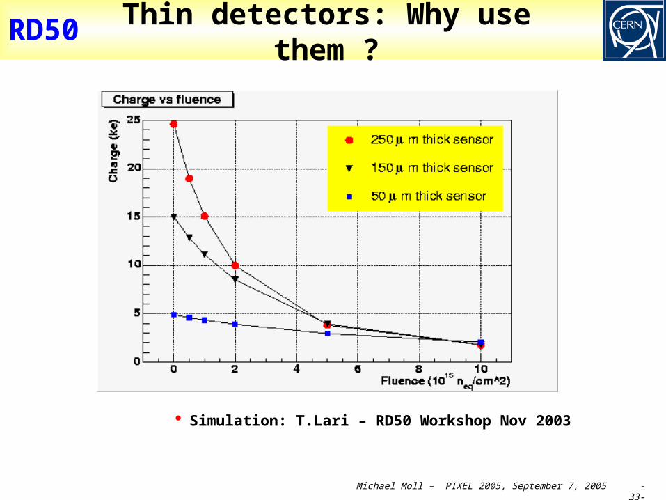
RD50 Thin detectors: Why use them ?
Simulation: T.Lari – RD50 Workshop Nov 2003