r09 set no. 2 - wordpress.com · code no: r09220402 r09 set no. 2 ii b.tech ii semester...
TRANSCRIPT
COURTESY IARE
Code No: R09220402 R09 Set No. 2
II B.Tech II Semester Examinations,Dec/Jan -2011/2012ELECTRONIC CIRCUIT ANALYSIS
Common to ICE, E.COMP.E, ETM, EIE, ECETime: 3 hours Max Marks: 75
Answer any FIVE QuestionsAll Questions carry equal marks
? ? ? ? ?
1. (a) Draw the circuit of a voltage series feedback circuit and explain it.
(b) What are the possible amplifiers circuits in any feedback system? Discuss.[8+7]
2. Obtain the expressions for the voltage gain in the low frequency, medium frequencyand high frequency ranges in the case of single stage amplifier. [15]
3. (a) Give the two Barkhausen conditions required in order for sinusoidal oscillationsto be sustained.
(b) Draw the circuit diagram of RC phase - shift oscillator and derive the expres-sion for frequency of Oscillations & condition for sustained Oscillations.
[5+10]
4. (a) Consider an emitter follower and show that as Re→∞ Ri = hie +1+hfe
hoe
(b) What is the maximum value of Rs for which Ro differs by no more than 10percent of its value for RS = 0 the transistor parameters are hfe = 50, hie =1.1k hre = 2.5×10⁻⁴, hoe = 24µA/V. [7+8]
5. (a) Why two tuned circuits are used in double tuned amplifier?
(b) What are the advantages of stagger tuned amplifier?
(c) Why parallel resonance circuits are used in tuned amplifiers? [5+5+5]
6. (a) Draw the FET amplifier equivalent circuit looking into the drain and find itsgain & o/p impedance?
(b) Starting with the definition of gm and rd, show that if two identical FETs areconnected in parallel, gm is doubled and rd is halved since µ = rdgm, then µremains unchanged. [8+7]
7. (a) Derive the expression for the bandwidth of multistage amplifier.
(b) What are the problems of Direct coupled amplifiers?
(c) Why RC coupling is popular?
(d) Why transformer coupling is not used in the initial stage of a multistageamplifier? [5+3+3+4]
8. (a) A single ended class A power amplifier is coupled to an 8Ω load, using atransformer with a turn ratio of 5:1 with a 50V supply the transistor is biasedto have a quiscent collector current of 250mA. When a sinusoidal signal is
1
State Miller's theorem and its dual.

COURTESY IARE
Code No: R09220402 R09 Set No. 2
applied to the base, the collector voltage varies between a maximum of 5V andmaximum of 90V. Estimate the efficiency, power output & second - harmonicdistortion of this stage.
(b) Discuss how rectification may takes place in a power amplifier? [8+7]
? ? ? ? ?
2
COURTESY IARE
Code No: R09220402 R09 Set No. 4
II B.Tech II Semester Examinations,Dec/Jan -2011/2012ELECTRONIC CIRCUIT ANALYSIS
Common to ICE, E.COMP.E, ETM, EIE, ECETime: 3 hours Max Marks: 75
Answer any FIVE QuestionsAll Questions carry equal marks
? ? ? ? ?
1. (a) In a colpitts oscillator, C1 = 0.2µF and C2 = 0.04µF. If the frequency ofoscillation is 10KHz, find the value if Inductor. Also, find the required gainfor oscillation.
(b) Determine the frequency of oscillations in a wien bridge oscillator? [8+7]
2. (a) Explain the Principle of opeartion of direct coupled amplifier and mention itsadvantages.
(b) What is the use of transformer coupling in the output stage of multi stageamplifier?
(c) Why RC coupling is mostly used for voltage amplifier. [8+4+3]
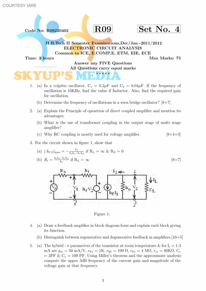
3. For the circuit shown in figure 1, show that
(a) (AV S)max = − hf
hiho−hrhfif RL = ∞ & RS = 0
(b) Ri =hiho−hrhf
hoif RL = ∞ [8+7]
Figure 1:
4. (a) Draw a feedback amplifier in block diagram form and explain each block givingits function.
(b) Distinguish between regenerative and degenerative feedback in amplifiers.[10+5]
5. (a) The hybrid - π parameters of the transistor at room temperature & for Ic = 1.3mA are gm = 50 mA/V, rb′e = 1K, rbb′ = 100 Ω, rb′c = 4 MΩ, rce = 80KΩ, Cc
= 3PF & Ce = 100 PF. Using Miller’s theorem and the approximate analysiscompute the upper 3dB frequency of the current gain and magnitude of thevoltage gain at that frequency.
3
COURTESY IARE
Code No: R09220402 R09 Set No. 4
(b) Consider a single - stage CE transistor amplifier with the load resistance RL
shunted by a capacitance CL. Prove that the internal voltage gain K isK ≈ −gmRL
1+jω(CC+CL)RL[8+7]
6. (a) Find the voltage gain of the circuit shown in figure 2 FET parameters are µ= 24, rd = 4K and also find voltage gain if the output impedance of the signalsource is 50K.
Figure 2:
(b) Derive an expression for voltage gain of common drain configuration & givethe expression for voltage of the amplifoer. [8+7]
7. (a) Compare neutralisation and unilaterlisation methods of tuned amplifiers.
(b) What are the limitations of stagger tuned amplifiers?
(c) What happen when no. of stages is increased in single tuned cascaded ampli-fiers? [5+5+5]
8. (a) Show that the maximum conversion efficiency of the idealized class B pus -pull circuit is 78.5%.
(b) For an ideal class B transistor amplifier the collector supply voltage Vcc andthe effective load resistance R1
L = (N1
N2)2 RL are fixed as the base current
excitation is varied. Show that the collector dissipation Pc is zero at no signal,rises as Vm increses and passes through a maximum at Vm = 2Vcc/π.
[8+7]
? ? ? ? ?
4
a) Show the .cbeb
ebre rr
rh′′
′
+=
b) Derive the equation for gain bandwidth product. c) Draw and explain a simplified high frequency model [5+5+5]
COURTESY IARE
Code No: R09220402 R09 Set No. 1
II B.Tech II Semester Examinations,Dec/Jan -2011/2012ELECTRONIC CIRCUIT ANALYSIS
Common to ICE, E.COMP.E, ETM, EIE, ECETime: 3 hours Max Marks: 75
Answer any FIVE QuestionsAll Questions carry equal marks
? ? ? ? ?
1. (a) A transistor in CB circuit has the following set of ‘h’ parameters. hib = 20Ω,hfb = 0.98, hrb = 3×10⁻⁴, hob = 0.5×10⁻⁶. Find the values if Ri, Ro, Ai & Av
if Rs = 600Ω and RL = 1.5 kΩ.
(b) Draw the CE amplifier with un by passed emitter resistance and derive ex-pression for its Ri & Av? [8+7]
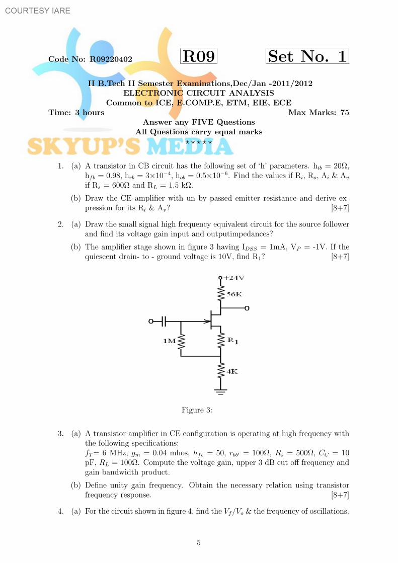
2. (a) Draw the small signal high frequency equivalent circuit for the source followerand find its voltage gain input and outputimpedances?
(b) The amplifier stage shown in figure 3 having IDSS = 1mA, VP = -1V. If thequiescent drain- to - ground voltage is 10V, find R1? [8+7]
Figure 3:
3. (a) A transistor amplifier in CE configuration is operating at high frequency withthe following specifications:fT = 6 MHz, gm = 0.04 mhos, hfe = 50, rbb′ = 100Ω, Rs = 500Ω, CC = 10pF, RL = 100Ω. Compute the voltage gain, upper 3 dB cut off frequency andgain bandwidth product.
(b) Define unity gain frequency. Obtain the necessary relation using transistorfrequency response. [8+7]
4. (a) For the circuit shown in figure 4, find the Vf/Vo & the frequency of oscillations.
5
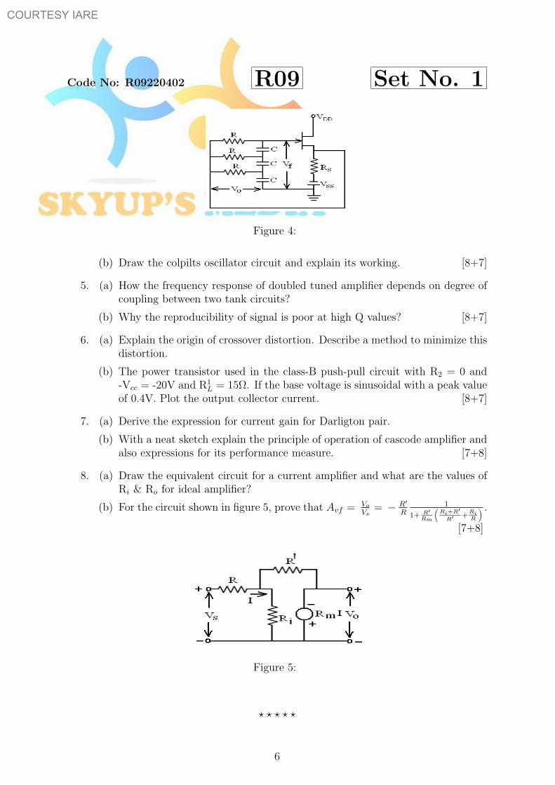
COURTESY IARE
Code No: R09220402 R09 Set No. 1
Figure 4:
(b) Draw the colpilts oscillator circuit and explain its working. [8+7]
5. (a) How the frequency response of doubled tuned amplifier depends on degree ofcoupling between two tank circuits?
(b) Why the reproducibility of signal is poor at high Q values? [8+7]
6. (a) Explain the origin of crossover distortion. Describe a method to minimize thisdistortion.
(b) The power transistor used in the class-B push-pull circuit with R2 = 0 and-Vcc = -20V and R1
L = 15Ω. If the base voltage is sinusoidal with a peak valueof 0.4V. Plot the output collector current. [8+7]
7. (a) Derive the expression for current gain for Darligton pair.
(b) With a neat sketch explain the principle of operation of cascode amplifier andalso expressions for its performance measure. [7+8]
8. (a) Draw the equivalent circuit for a current amplifier and what are the values ofRi & Ro for ideal amplifier?
(b) For the circuit shown in figure 5, prove that Avf = Vo
Vs= − R′
R1
1+ R′Rm
(Ri+R′
R′ +RiR
) .
[7+8]
Figure 5:
? ? ? ? ?
6
COURTESY IARE
Code No: R09220402 R09 Set No. 3
II B.Tech II Semester Examinations,Dec/Jan -2011/2012ELECTRONIC CIRCUIT ANALYSIS
Common to ICE, E.COMP.E, ETM, EIE, ECETime: 3 hours Max Marks: 75
Answer any FIVE QuestionsAll Questions carry equal marks
? ? ? ? ?
1. (a) The open loop gain of an amplifier is 100. What will be the overall gain whena negative feed back of 0.5 is applied to the amplifier?
(b) What are the different mixing techniques used in any feed back system? Ex-plain.
(c) State the condition in terms of (1 + Aβ) which a feed back amplifier mustsatisfy in order to be stable. [4+4+7]
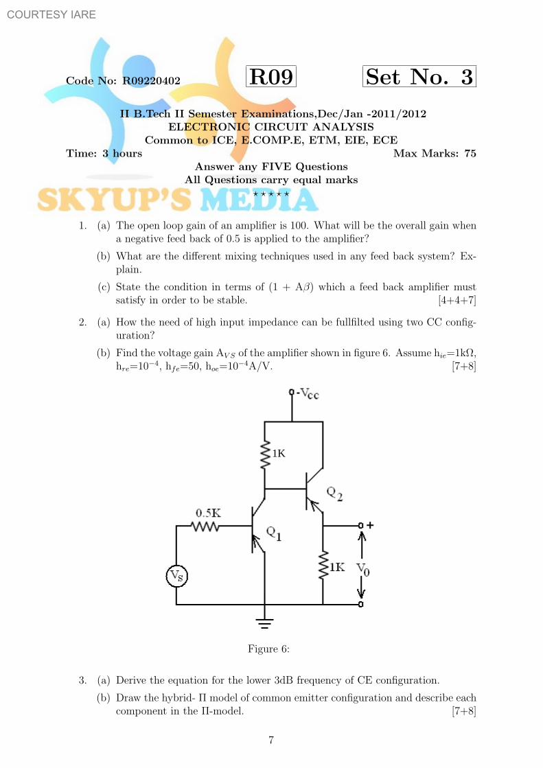
2. (a) How the need of high input impedance can be fullfilted using two CC config-uration?
(b) Find the voltage gain AV S of the amplifier shown in figure 6. Assume hie=1kΩ,hre=10−4, hfe=50, hoe=10−4A/V. [7+8]
Figure 6:
3. (a) Derive the equation for the lower 3dB frequency of CE configuration.
(b) Draw the hybrid- Π model of common emitter configuration and describe eachcomponent in the Π-model. [7+8]
7
1K
COURTESY IARE
Code No: R09220402 R09 Set No. 3
4. (a) What is class B amplifier? Why is it employed? Give its circuits, designequations, characteristics & limitations.
(b) A transformer coupled class A large signal amplifier has maximum and min-imum values of collector to emitter voltage of 25V and 2.5V. Determine itscollector efficiency. [10+5]
5. (a) Draw the equivalent circuit of double tuned amplifier and derive the expressionfor gain at resonance.
(b) Derive the expression for effective bandwidth of cascaded tuned amplifier.[8+7]
6. (a) Derive an expression for voltage gain of a common source FET amplifier withand without source resistance included in the circuit.
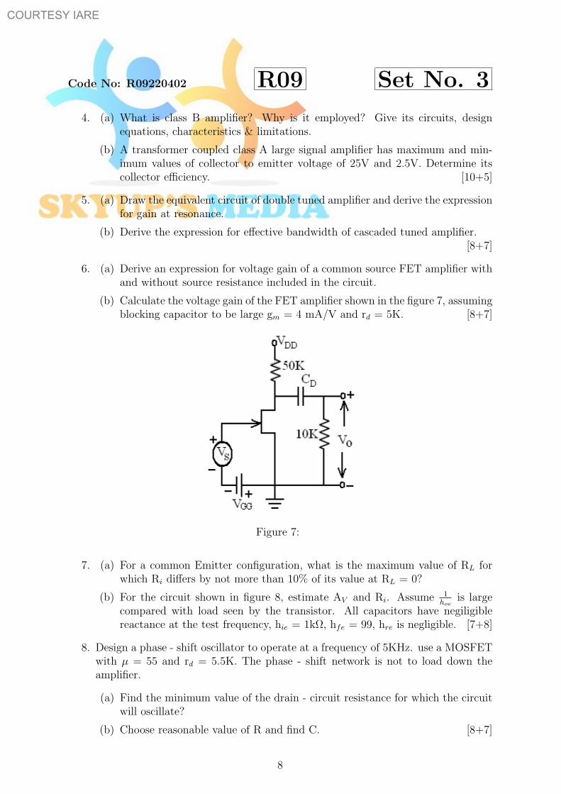
(b) Calculate the voltage gain of the FET amplifier shown in the figure 7, assumingblocking capacitor to be large gm = 4 mA/V and rd = 5K. [8+7]
Figure 7:
7. (a) For a common Emitter configuration, what is the maximum value of RL forwhich Ri differs by not more than 10% of its value at RL = 0?
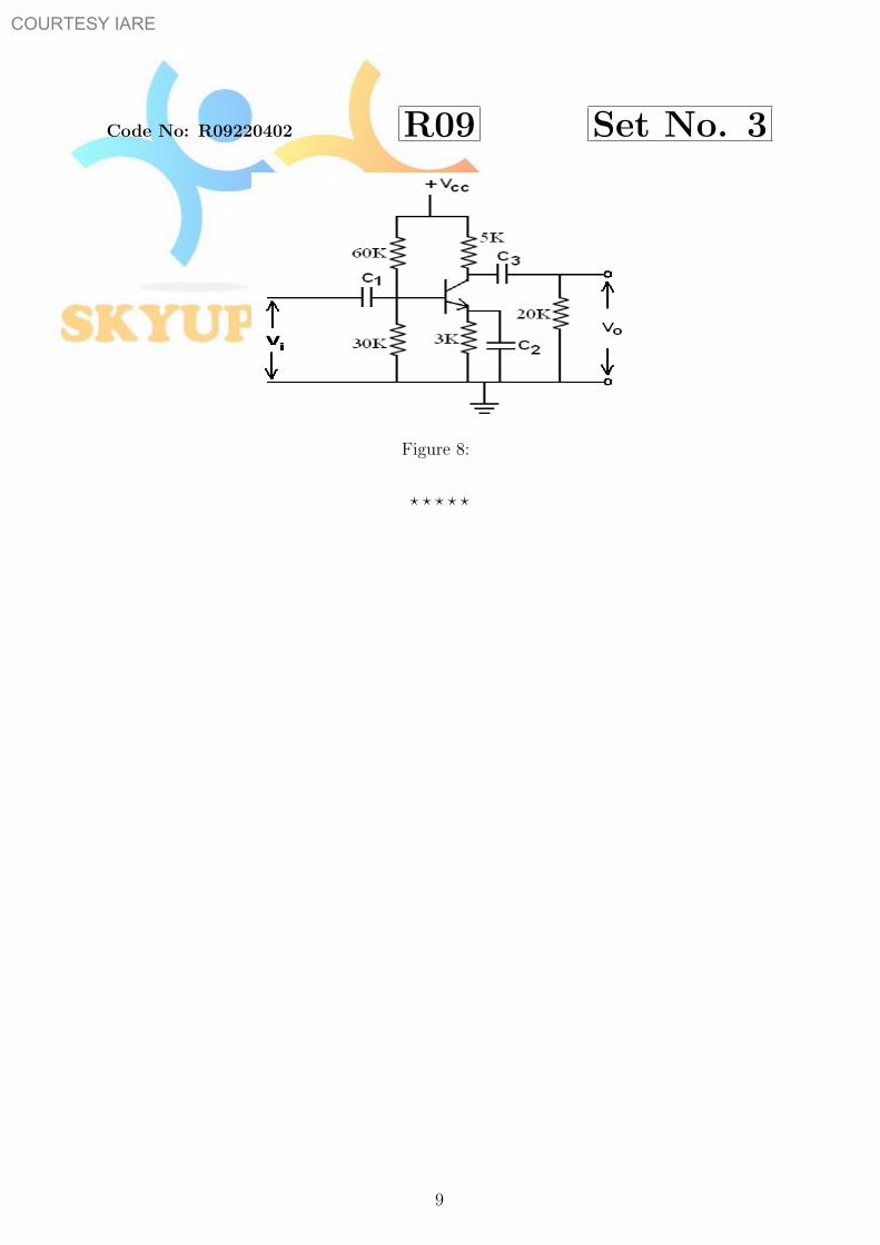
(b) For the circuit shown in figure 8, estimate AV and Ri. Assume 1hoe
is largecompared with load seen by the transistor. All capacitors have negiligiblereactance at the test frequency, hie = 1kΩ, hfe = 99, hre is negligible. [7+8]
8. Design a phase - shift oscillator to operate at a frequency of 5KHz. use a MOSFETwith µ = 55 and rd = 5.5K. The phase - shift network is not to load down theamplifier.
(a) Find the minimum value of the drain - circuit resistance for which the circuitwill oscillate?
(b) Choose reasonable value of R and find C. [8+7]
8
COURTESY IARE
Code No: R09220402 R09 Set No. 3
Figure 8:
? ? ? ? ?
9
COURTESY IARE
Code No: R09220402 JAWAHARLAL NEHRU TECHNOLOGICAL UNIVERSITY, HYDERABAD
B. Tech II Year - II Semester Examinations, November/December, 2012 ELECTRONIC CIRCUIT ANALYSIS
(COMMON TO ECE, ETM, ICE, E.COMP.E, EIE) Time: 3 hours Max. Marks: 75
Answer any five questions All questions carry equal marks
- - - 1.a) State Miller’s Theorem. b) Derive the expressions for the Voltage gain, input resistance and output resistance
of common collector circuit, using simplified Hybrid Model. [5+10] 2. Two BJT CE amplifiers in self biasing configuration are connected in cascade.
The following are the parameters of each circuit: The biasing resistors are R1 = 10KΩ; R2 = 5KΩ; Collector resistor Rc = 2KΩ;
Emitter Resistor Re=2KΩ. hie=1KΩ; hfe=100. Neglect the effect of hoe. Calculate the Voltage gain, input impedance and output impedance of the above cascade. [15]
3.a) Draw the Hybrid-π model for a common emitter transistor and explain. b) Explain about Gain-Bandwidth Product of an amplifier. [10+5] 4.a) Draw and explain the small signal model of a MOS amplifier. b) Derive the expression for the voltage gain of a MOS-Source Follower. [7+8] 5.a) Explain and justify the effect of Nagative feed back on the characteristics of an
amplifier. b) An amplifier with open loop gain of 2000±150 is available. It is necessary to have
the amplifier whose voltage gain varies by not more than ±0.2%. Calculate the feedback factor β, and the gain of the amplifier with feedback. [10+5]
6. Derive the expression for the frequency of oscillations of a BJT-RC Phase shift
Oscillator. [15] 7.a) Derive the expression for the efficiency of a direct coupled Class-A amplifier. b) What is crossover distortion? Explain. [10+5] 8. Write notes on the following: a) Stagger Tuning b) Single Tuned and Double Tuned Amplifiers. [7+8] *******
R09
www.engineershub.in www.engineershub.in
Enginee
rshub
En
gin
eersHu
b A
nd
roid
Ap
p E
ng
ineersH
ub
An
dro
id A
pp
COURTESY IARE
R09 SET No - 1CODE NO: R09220402
II B.TECH - II SEMESTER EXAMINATIONS, APRIL/MAY, 2011 ELECTRONIC CIRCUIT ANALYSIS
(Common to Electronics & Communication Systems, Electronics & Computer Engineering, Electronics & Instrumentation Engineering, Electronics & Telematics,
Instrumentation & Control Engineering) Time: 3hours Max. Marks: 75
Answer any FIVE questions All Questions Carry Equal Marks
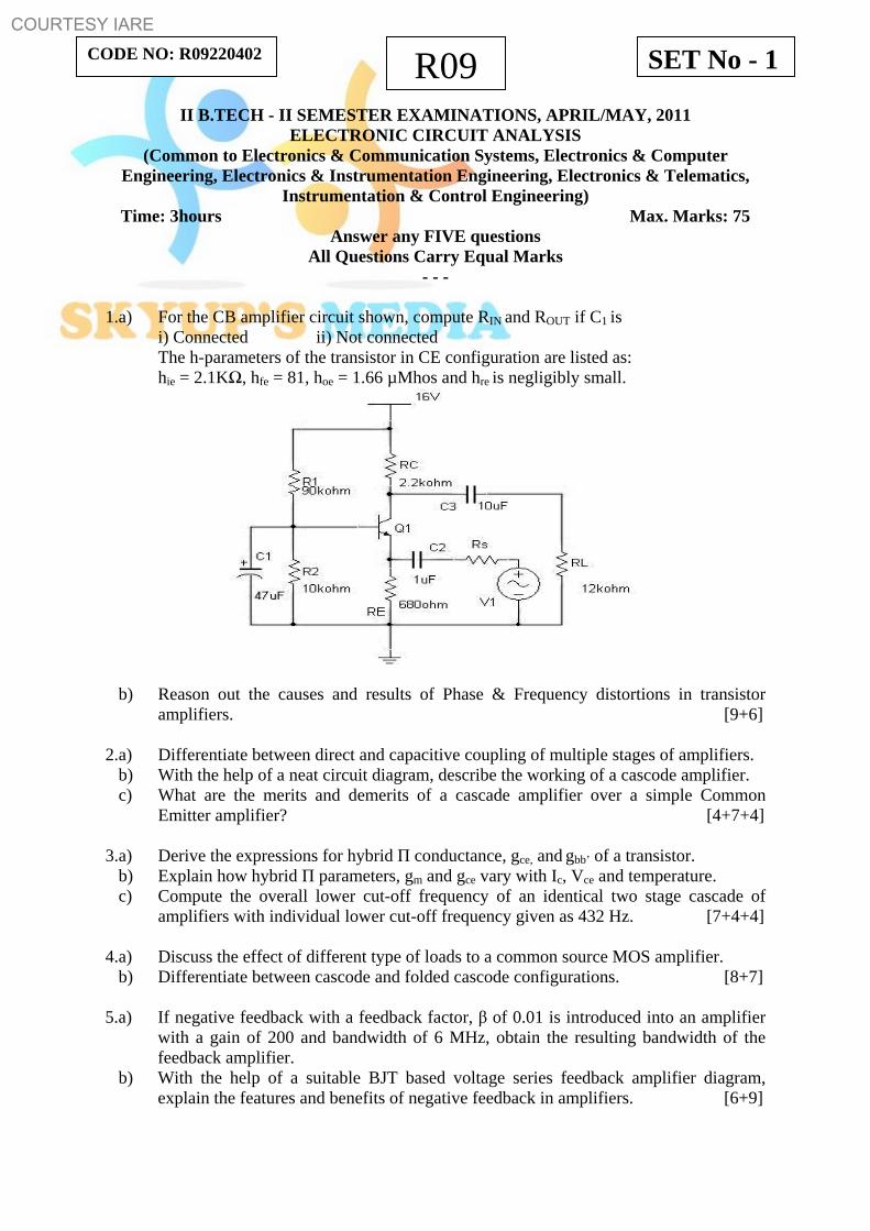
- - - 1.a) For the CB amplifier circuit shown, compute RIN and ROUT if C1 is
i) Connected ii) Not connected The h-parameters of the transistor in CE configuration are listed as: hie = 2.1KΩ, hfe = 81, hoe = 1.66 µMhos and hre is negligibly small.
b) Reason out the causes and results of Phase & Frequency distortions in transistor
amplifiers. [9+6] 2.a) Differentiate between direct and capacitive coupling of multiple stages of amplifiers. b) With the help of a neat circuit diagram, describe the working of a cascode amplifier. c) What are the merits and demerits of a cascade amplifier over a simple Common
Emitter amplifier? [4+7+4] 3.a) Derive the expressions for hybrid Π conductance, gce, and gbb’ of a transistor.
b) Explain how hybrid Π parameters, gm and gce vary with Ic, Vce and temperature. c) Compute the overall lower cut-off frequency of an identical two stage cascade of
amplifiers with individual lower cut-off frequency given as 432 Hz. [7+4+4] 4.a) Discuss the effect of different type of loads to a common source MOS amplifier. b) Differentiate between cascode and folded cascode configurations. [8+7] 5.a) If negative feedback with a feedback factor, β of 0.01 is introduced into an amplifier
with a gain of 200 and bandwidth of 6 MHz, obtain the resulting bandwidth of the feedback amplifier.
b) With the help of a suitable BJT based voltage series feedback amplifier diagram, explain the features and benefits of negative feedback in amplifiers. [6+9]
COURTESY IARE
6.a) Substantiate the requirement of positive feedback in amplifier for oscillations. Relate
the requirement to Barkhausen Criterion. b) With the help of neat circuit diagram, explain how sustained oscillations are obtained
in RC phase shift BJT based oscillator. Derive the expression for frequency of oscillation. [6+9]
7.a) A single stage class A amplifier Vcc=20V, VCEQ =10V, ICQ =600mA, RL=16 Ω. The ac
output current varies by 300mA, with the ac input signal. Find ±i) The power supplied by the dc source to the amplifier circuit. ii) AC power consumed by the load resistor. iii) AC power developed across the load resistor. iv) DC power wasted in transistor collector. v) Overall efficiency vi) Collector efficiency.
b). List the advantages of complementary-symmetry configuration over push pull configuration. [9+6]
8. Describe the following briefly: a) Stagger Tuned Amplifiers – Operation and comparison with synchronous tuning b) Heat Sinks for tuned power amplifiers. [8+7]
********
COURTESY IARE
R09 SET No - 2CODE NO: R09220402
II B.TECH - II SEMESTER EXAMINATIONS, APRIL/MAY, 2011 ELECTRONIC CIRCUIT ANALYSIS
(Common to Electronics & Communication Systems, Electronics & Computer Engineering, Electronics & Instrumentation Engineering, Electronics & Telematics,
Instrumentation & Control Engineering) Time: 3hours Max. Marks: 75
Answer any FIVE questions All Questions Carry Equal Marks
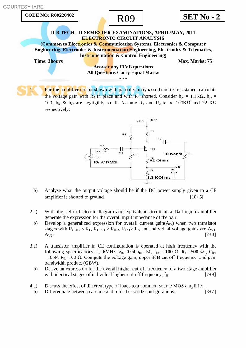
- - - 1. For the amplifier circuit shown with partially unbypassed emitter resistance, calculate
the voltage gain with R4 in place and with R4 shorted. Consider hie = 1.1KΩ, hfe = 100, hre & hoe are negligibly small. Assume R1 and R2 to be 100KΩ and 22 KΩ respectively.
b) Analyse what the output voltage should be if the DC power supply given to a CE
amplifier is shorted to ground. [10+5]
2.a) With the help of circuit diagram and equivalent circuit of a Darlington amplifier
generate the expression for the overall input impedance of the pair. b) Develop a generalized expression for overall current gain(AIS) when two transistor
stages with ROUT2 < RL, ROUT1 > RIN2, RIN1> RS and individual voltage gains are AV1, AV2. [7+8]
3.a) A transistor amplifier in CE configuration is operated at high frequency with the
following specifications. fT=6MHz, gm=0.04,hfe =50, rbb’ =100 Ω, Rs =500 Ω , Cb’c =10pF, RL=100 Ω. Compute the voltage gain, upper 3dB cut-off frequency, and gain bandwidth product (GBW).
b) Derive an expression for the overall higher cut-off frequency of a two stage amplifier with identical stages of individual higher cut-off frequency, fH. [7+8]
4.a) Discuss the effect of different type of loads to a common source MOS amplifier. b) Differentiate between cascode and folded cascode configurations. [8+7]
COURTESY IARE
5.a). If the non-linear distortion in a negative feedback amplifier with an open loop gain of 100 is reduced from 40% to 10%with feedback, compute the feedback factor, β of the amplifier.
b) Draw the circuit diagram of a current series feedback amplifier, Derive expressions to show the effect of negative feedback on input & output impedances, bandwidth, distortion of the amplifier. [6+9]
6.a) Differentiate between RC and LC type oscillators. b) Derive the expression for frequency of oscillation in a Hartley Oscillator. c) State Barkhausen Critterion for Oscillations [5+7+3] 7.a) Derive the expression for maximum conversion efficiency for a simple series fed
Class A power amplifier. b) What are the drawbacks of transformer coupled power amplifiers? c) A push pull amplifier utilizes a transformer whose primary has a total of 160 turns
and whose secondary has 40 turns. It must be capable of delivering 40W to an 8 Ω load under maximum power conditions. What is the minimum possible value of Vcc?
[5+4+6] 8.a) List possible configurations of tuned amplifiers.
b) Derive an expression for bandwidth of a capacitive coupled tuned amplifier in CE configuration. Make necessary assumptions and mention them. [6+9]
********
COURTESY IARE
R09 SET No - 3CODE NO: R09220402
II B.TECH - II SEMESTER EXAMINATIONS, APRIL/MAY, 2011 ELECTRONIC CIRCUIT ANALYSIS
(Common to Electronics & Communication Systems, Electronics & Computer Engineering, Electronics & Instrumentation Engineering, Electronics & Telematics,
Instrumentation & Control Engineering) Time: 3hours Max. Marks: 75
Answer any FIVE questions All Questions Carry Equal Marks
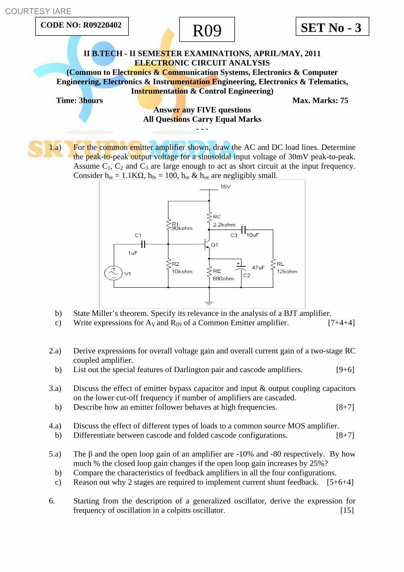
- - - 1.a) For the common emitter amplifier shown, draw the AC and DC load lines. Determine
the peak-to-peak output voltage for a sinusoidal input voltage of 30mV peak-to-peak. Assume C1, C2 and C3 are large enough to act as short circuit at the input frequency. Consider hie = 1.1KΩ, hfe = 100, hre & hoe are negligibly small.
b) State Miller’s theorem. Specify its relevance in the analysis of a BJT amplifier. c) Write expressions for AV and RIN of a Common Emitter amplifier. [7+4+4] 2.a) Derive expressions for overall voltage gain and overall current gain of a two-stage RC
coupled amplifier. b) List out the special features of Darlington pair and cascode amplifiers. [9+6] 3.a) Discuss the effect of emitter bypass capacitor and input & output coupling capacitors
on the lower cut-off frequency if number of amplifiers are cascaded. b) Describe how an emitter follower behaves at high frequencies. [8+7] 4.a) Discuss the effect of different types of loads to a common source MOS amplifier. b) Differentiate between cascode and folded cascode configurations. [8+7] 5.a) The β and the open loop gain of an amplifier are -10% and -80 respectively. By how
much % the closed loop gain changes if the open loop gain increases by 25%? b) Compare the characteristics of feedback amplifiers in all the four configurations. c) Reason out why 2 stages are required to implement current shunt feedback. [5+6+4] 6. Starting from the description of a generalized oscillator, derive the expression for
frequency of oscillation in a colpitts oscillator. [15]

COURTESY IARE
7.a) With the help of a suitable circuit diagram, show that the maximum conversion
efficiency of a class B power amplifier is 78.5%. b) Explain how Total harmonic distortion can be reduced in a Class B push-pull
configured amplifier. [7+8] 8.a) Derive an expression for the bandwidth of a synchronous tuned circuit. b) Discuss the necessity of stabilization circuits in tuned amplifiers. [8+7]
********
COURTESY IARE
R09 SET No - 4CODE NO: R09220402
II B.TECH - II SEMESTER EXAMINATIONS, APRIL/MAY, 2011 ELECTRONIC CIRCUIT ANALYSIS
(Common to Electronics & Communication Systems, Electronics & Computer Engineering, Electronics & Instrumentation Engineering, Electronics & Telematics,
Instrumentation & Control Engineering) Time: 3hours Max. Marks: 75
Answer any FIVE questions All Questions Carry Equal Marks
- - - 1.a) Draw the circuit diagram of a common collector amplifier along with its equivalent
circuit. Derive expressions for AV and RI. b) What is meant by small signal for analyzing a BJT based amplifier? c) What is non-linear distortion? List the causes for this type of distortion in amplifiers. [7+4+4] 2.a) Discuss various possibilities of inter-stage coupling of amplifiers.
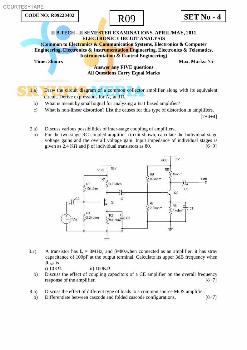
b) For the two-stage RC coupled amplifier circuit shown, calculate the Individual stage voltage gains and the overall voltage gain. Input impedance of individual stages is given as 2.4 KΩ and β of individual transistors as 80. [6+9]
3.a) A transistor has fα = 8MHz, and β=80.when connected as an amplifier, it has stray
capacitance of 100pF at the output terminal. Calculate its upper 3dB frequency when Rload is i) 10KΩ ii) 100KΩ.
b) Discuss the effect of coupling capacitors of a CE amplifier on the overall frequency response of the amplifier. [8+7]
4.a) Discuss the effect of different type of loads to a common source MOS amplifier. b) Differentiate between cascode and folded cascode configurations. [8+7]
COURTESY IARE
5.a) An amplifier has a gain of 50 with negative feedback. For a specified output voltage, if the input required is 0.1V without feedback and 0.8V with feedback, Compute β and open loop gain.
b) Through the block schematics, show four types of negative feedback in amplifiers. c) List the advantages of negative feedback in amplifiers. [5+5+5] 6.a) List out the merits × demerits of oscillators.
b) With the help of suitable schematic and description, show that both positive and negative feedback are used in a Wien Bridge oscillator. Establish the condition for oscillations. [7+8]
7.a) State the merits of using push pull configuration? Describe the operation of class B
push pull amplifier and show how even harmonics are eliminated. b) A single ended class A amplifier has a transformer coupled load of 8 Ω. If the
transformer turns ration is 10, find the maximum power output delivered to the load. Take the zero signal collector current of 500mA. [7+8]
8.a) Derive the expressions for Bandwidth and Q-factor of single tuned, capacitively
coupled amplifiers. List the assumptions made for the derivation. b) What is stagger tuning? Suggest possible applications. [9+6]
********