queued output match tpu function...
TRANSCRIPT
Order this document by TPUPN01/D
PROGRAMMING NOTE
Fre
esc
ale
Se
mic
on
du
cto
r, I
nc
...
Queued Output Match TPU Function (QOM)By Jeff Wright
1 Functional OverviewThe QOM function generates complex pulse trains without CPU intervention using a sequence of outputmatches. An output match causes a programmable pin response when a user-defined value is matchedby the value of a free-running counter. QOM generates multiple output matches using a queue of offsettimes and pin responses in parameter RAM. Queue size can vary from application to application. Vari-ous modes of queued operation are supported.
2 Detailed DescriptionEntries in the QOM queue are incremental match offsets, not absolute match times. The next matchtime in a sequence is calculated by adding the next queued offset to the time of the last match. If thematch is the first match in a sequence, the first offset value in the queue is added to a selectable refer-ence time.
The reference time from which the first match in a sequence is scheduled can be the immediate valueof the selected TCR, the time of the last match of a previous sequence, or a time contained in parameterRAM. Using the time of the last match of a previous sequence as a reference allows a series of se-quences to be chained together. Using a time value from parameter RAM allows a chain of outputmatches to be referenced to a time derived by another TPU channel.
Pin response (high or low transition) when a match occurs is fully programmable. Pin response is de-termined by the value of bit 0 in each queue entry.
The function can operate in single-shot mode, in which a sequence of match outputs is generated once;in loop mode, in which a sequence of match outputs is generated a specified number of times (1 to 256),or in continuous mode; in which the entire sequence repeats until the channel is disabled or the TPUreceives a new host service request. Linked operation allows the function to be triggered by a link fromanother TPU channel. All loop modes can be used in conjunction with linked operation.
In single-shot mode and in loop mode, the event time of the last match in the queue is written back intoparameter RAM for the CPU to access. Three host service states allow the function to be initiated withthe output pin high, low, or with no change in state.
If adjacent queue offset values are programmed for the same pin response, duration of an output eventcan effectively be extended beyond the normal $8000 TCR-count limit imposed by the TPU greater-than-or-equal-to comparator.
A detailed description of the QOM algorithm, including a state diagram, is provided for reference at theend of this document.
3 Function Code SizeTotal TPU function code size determines what combination of functions can fit into a given ROM or em-ulation memory microcode space. QOM function code size is:
41 µ instructions + 8 entries = 49 long words
For More Information On This Product,
Go to: www.freescale.com
Fre
esc
ale
Se
mic
on
du
cto
r, I
Freescale Semiconductor, Inc.n
c..
.
4 Function ParametersThis section provides detailed descriptions of function parameters stored in channel parameter RAM.Figure 1 shows TPU parameter RAM address mapping. Figure 2 shows the parameter RAM assign-ment used by the function. In the diagrams, Y = M111, where M is the value of the module mapping bit(MM) in the system integration module configuration register (Y = $7 or $F).
— = Not Implemented (reads as $00)
Figure 1 TPU Channel Parameter RAM CPU Address Map
Channel Base Parameter Address
Number Address 0 1 2 3 4 5 6 7
0 $YFFF## 00 02 04 06 08 0A — —
1 $YFFF## 10 12 14 16 18 1A — —
2 $YFFF## 20 22 24 26 28 2A — —
3 $YFFF## 30 32 34 36 38 3A — —
4 $YFFF## 40 42 44 46 48 4A — —
5 $YFFF## 50 52 54 56 58 5A — —
6 $YFFF## 60 62 64 66 68 6A — —
7 $YFFF## 70 72 74 76 78 7A — —
8 $YFFF## 80 82 84 86 88 8A — —
9 $YFFF## 90 92 94 96 98 9A — —
10 $YFFF## A0 A2 A4 A6 A8 AA — —
11 $YFFF## B0 B2 B4 B6 B8 BA — —
12 $YFFF## C0 C2 C4 C6 C8 CA — —
13 $YFFF## D0 D2 D4 D6 D8 DA — —
14 $YFFF## E0 E2 E4 E6 E8 EA EC EE
15 $YFFF## F0 F2 F4 F6 F8 FA FC FE
TPU Programming Library2 TPUPN01/D
For More Information On This Product,
Go to: www.freescale.com
Fre
esc
ale
Se
mic
on
du
cto
r, I
Freescale Semiconductor, Inc.n
c..
.
* Not available on all channelsW = Channel number
Figure 2 QOM Function Parameter RAM Assignment
15 14 13 12 11 10 9 8 7 6 5 4 3 2 1 0
$YFFFW0 REF_ADDR B LAST_OFF_ADDR A
$YFFFW2 LOOP_CNT (LAST_MATCH_TIM) OFF_PTR C
$YFFFW4 OFFSET_1 ∞$YFFFW6 OFFSET_2 ∞$YFFFW8 OFFSET_3 ∞$YFFFWA OFFSET_4 ∞$YFFFWC OFFSET_5* ∞$YFFFWE OFFSET_6* ∞
$YFFF (W + 1) 0 OFFSET_7* ∞$YFFF (W + 1) 2 OFFSET_8* ∞
⇓ ⇓ ⇓$YFFF (W + 1) 14 OFFSET_14* ∞
Parameter Write Access
Written by CPU
Written by TPU
Written by CPU and TPU
Unused parameters
Bit Encoding
A Timebase Selection
0 Use TCR1 as Timebase
1 Use TCR2 as Timebase
∞ Edge Selection
0 Falling Edge at Match
1 Rising Edge at Match
B:C Reference for First Match
00 Immediate TCR Value
01 Last Event Time
10 Value Pointed to by REF_ADDR
11 Last Event Time
TPU Programming LibraryTPUPN01/D 3
For More Information On This Product,
Go to: www.freescale.com
Fre
esc
ale
Se
mic
on
du
cto
r, I
Freescale Semiconductor, Inc.n
c..
.
4.1 BIT_A
This control bit determines which of the two TPU timer counters is used as a timebase for an outputmatch sequence. The timer counter is selected during the host service request states and the link state(states 1, 2, 3, 4). When BIT_A is equal to zero, TCR1 is selected as the timebase. When BIT_A is equalto one, TCR2 is selected.
4.2 LAST_OFF_ADDR
This parameter contains the upper seven bits of the PRAM address of the last entry in the match offsetqueue (for example, a value of%0001101 indicates parameter 5 of channel 1 is the last queue entry). Itis used during the match state (state 5) to determine when the end of the queue has been reached.
4.3 BIT_B
This control bit and BIT_C are used during the host service and link states (states 1, 2, 3, 4) to determinethe reference time for the first match after initialization. Reference time can be:
An immediate TCR value
A value in parameter RAM pointed to by REF_ADDR
The event time of the last match in the previous sequence of matches.
4.4 REF_ADDR
When the values of BIT_B and BIT_C select a value in parameter RAM as a reference time for the firstmatch after initialization, this parameter contains the upper seven bits of the PRAM address of the valueto be used. When an immediate TCR reference or last event reference is selected, it is unnecessary toprovide a REF_ADDR value.
4.5 OFF_PTR
This 7-bit parameter is normally used as a queue pointer. It is updated by the TPU after each matchoccurs. OFF_PTR value also determines whether linked operation is selected. If OFF_PTR contains anon-zero value during a host service state, linked operation is selected. In single-shot mode or loopmode, OFF_PTR is overwritten by LAST_MATCH_TIM at the end of the match sequence.
4.6 BIT_C
This control bit and BIT_B are used during the host service and link states (states 1, 2, 3, 4) to determinethe reference time for the first match after initialization. Reference time can be:
An immediate TCR value
A value in parameter RAM pointed to by REF_ADDR
The event time of the last match in the previous sequence of matches.
4.7 LOOP_CNT
This parameter is used as a counter during loop mode operation. The value in LOOP_CNT determineshow many times the queued match sequence is repeated. LOOP_CNT is initialized by the CPU anddecremented toward zero by the TPU. When LOOP_CNT reaches $00 after decrementing, the functionstops and LOOP_CNT is overwritten by LAST_MATCH_TIM. If LOOP_CNT is initialized to $00, thefunction loops 256 times.
TPU Programming Library4 TPUPN01/D
For More Information On This Product,
Go to: www.freescale.com
Fre
esc
ale
Se
mic
on
du
cto
r, I
Freescale Semiconductor, Inc.n
c..
.
4.8 LAST_MATCH_TIM
This parameter stores the time of the last match event in a sequence. The TPU stores the value aftercompletion of a match sequence during single-shot mode or loop mode operation. OFF_PTR,LOOP_CNT and BIT_C are overwritten by the LAST_MATCH_TIM value. LAST_MATCH_TIM is writ-ten after the last match has occurred but before the TPU requests interrupt service from the CPU.
4.9 OFFSET_N
These parameters form the match offset queue. The 15 upper bits of each parameter contain a shiftedoffset. The offset value is shifted right once before being used. This means that the maximum offsetfrom a previous match time or reference time is $7FFF TCR counts. Bit 0 of the offset parameter deter-mines whether a pin goes high or low as a result of a match event. When bit 0 is equal to zero, the pingoes low; when it is equal to one, the pin goes high. To program a pin to go high $1000 TCR countsafter the previous match, for example, the CPU must store a value of $2001 in the appropriateOFFSET_N parameter.
There can be from one to fourteen queue entries, depending upon which TPU channels are assignedto the QOM function. When channels 0 to 13 are used, the maximum number of entries is four; whenchannels 14 and 15 are used, the maximum number of entries is normally six. Table length is deter-mined by the value of LAST_OFF_ADDR, which points to the last queue entry. There is one specialcase — when channel 15 is not being used, the channel 14 LAST_OFF_ADDR pointer can be set topoint into channel 15 PRAM, providing up to 14 table queue entries.
Offsets in the queue are used in sequence, starting with OFFSET_1. OFFSET_1 must always be thethird parameter in QOM channel parameter RAM.
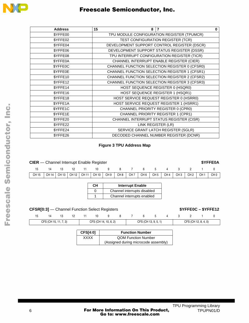
5 Host Interface to FunctionThis section provides information concerning the TPU host interface to the QOM function. Figure 3 is aTPU address map. Detailed TPU register diagrams follow the figure. In the diagrams, Y = M111, whereM is the value of the module mapping bit (MM) in the system integration module configuration register(Y = $7 or $F).
TPU Programming LibraryTPUPN01/D 5
For More Information On This Product,
Go to: www.freescale.com
Fre
esc
ale
Se
mic
on
du
cto
r, I
Freescale Semiconductor, Inc.n
c..
.
Figure 3 TPU Address Map
Address 15 8 7 0$YFFE00 TPU MODULE CONFIGURATION REGISTER (TPUMCR)$YFFE02 TEST CONFIGURATION REGISTER (TCR)$YFFE04 DEVELOPMENT SUPPORT CONTROL REGISTER (DSCR)$YFFE06 DEVELOPMENT SUPPORT STATUS REGISTER (DSSR)$YFFE08 TPU INTERRUPT CONFIGURATION REGISTER (TICR)$YFFE0A CHANNEL INTERRUPT ENABLE REGISTER (CIER)$YFFE0C CHANNEL FUNCTION SELECTION REGISTER 0 (CFSR0)$YFFE0E CHANNEL FUNCTION SELECTION REGISTER 1 (CFSR1)$YFFE10 CHANNEL FUNCTION SELECTION REGISTER 2 (CFSR2)$YFFE12 CHANNEL FUNCTION SELECTION REGISTER 3 (CFSR3)$YFFE14 HOST SEQUENCE REGISTER 0 (HSQR0)$YFFE16 HOST SEQUENCE REGISTER 1 (HSQR1)$YFFE18 HOST SERVICE REQUEST REGISTER 0 (HSRR0)$YFFE1A HOST SERVICE REQUEST REGISTER 1 (HSRR1)$YFFE1C CHANNEL PRIORITY REGISTER 0 (CPR0)$YFFE1E CHANNEL PRIORITY REGISTER 1 (CPR1)$YFFE20 CHANNEL INTERRUPT STATUS REGISTER (CISR)$YFFE22 LINK REGISTER (LR)$YFFE24 SERVICE GRANT LATCH REGISTER (SGLR)$YFFE26 DECODED CHANNEL NUMBER REGISTER (DCNR)
CIER — Channel Interrupt Enable Register $YFFE0A
15 14 13 12 11 10 9 8 7 6 5 4 3 2 1 0
CH 15 CH 14 CH 13 CH 12 CH 11 CH 10 CH 9 CH 8 CH 7 CH 6 CH 5 CH 4 CH 3 CH 2 CH 1 CH 0
CH Interrupt Enable0 Channel interrupts disabled1 Channel interrupts enabled
CFSR[0:3] — Channel Function Select Registers $YFFE0C – $YFFE12
15 14 13 12 11 10 9 8 7 6 5 4 3 2 1 0
CFS (CH 15, 11, 7, 3) CFS (CH 14, 10, 6, 2) CFS (CH 13, 9, 5, 1) CFS (CH 12, 8, 4, 0)
CFS[4:0] Function NumberXXXX QOM Function Number
(Assigned during microcode assembly)
TPU Programming Library6 TPUPN01/D
For More Information On This Product,
Go to: www.freescale.com
Fre
esc
ale
Se
mic
on
du
cto
r, I
Freescale Semiconductor, Inc.n
c..
.
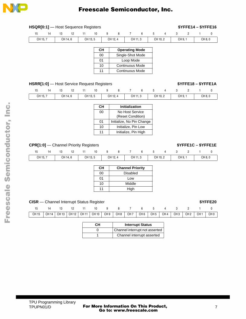
HSQR[0:1] — Host Sequence Registers $YFFE14 – $YFFE16
15 14 13 12 11 10 9 8 7 6 5 4 3 2 1 0
CH 15, 7 CH 14, 6 CH 13, 5 CH 12, 4 CH 11, 3 CH 10, 2 CH 9, 1 CH 8, 0
CH Operating Mode00 Single-Shot Mode01 Loop Mode10 Continuous Mode11 Continuous Mode
HSRR[1:0] — Host Service Request Registers $YFFE18 – $YFFE1A
15 14 13 12 11 10 9 8 7 6 5 4 3 2 1 0
CH 15, 7 CH 14, 6 CH 13, 5 CH 12, 4 CH 11, 3 CH 10, 2 CH 9, 1 CH 8, 0
CH Initialization00 No Host Service
(Reset Condition)01 Initialize, No Pin Change10 Initialize, Pin Low11 Initialize, Pin High
CPR[1:0] — Channel Priority Registers $YFFE1C – $YFFE1E
15 14 13 12 11 10 9 8 7 6 5 4 3 2 1 0
CH 15, 7 CH 14, 6 CH 13, 5 CH 12, 4 CH 11, 3 CH 10, 2 CH 9, 1 CH 8, 0
CH Channel Priority00 Disabled 01 Low10 Middle11 High
CISR — Channel Interrupt Status Register $YFFE20
15 14 13 12 11 10 9 8 7 6 5 4 3 2 1 0
CH 15 CH 14 CH 13 CH 12 CH 11 CH 10 CH 9 CH 8 CH 7 CH 6 CH 5 CH 4 CH 3 CH 2 CH 1 CH 0
CH Interrupt Status0 Channel interrupt not asserted 1 Channel interrupt asserted
TPU Programming LibraryTPUPN01/D 7
For More Information On This Product,
Go to: www.freescale.com
Fre
esc
ale
Se
mic
on
du
cto
r, I
Freescale Semiconductor, Inc.n
c..
.
6 Function ConfigurationThe CPU configures the QOM function as follows.
1. The appropriate channel priority bits are cleared, disabling the channel.2. The QOM function number is written to the channel function select bits. 3. BIT_A, BIT_B, BIT_C, LAST_OFF_ADDR, REF_ADDR (if required), OFF_PTR, LOOP_CNT
and queue values OFFSET_1 through OFFSET_N are written to channel parameter RAM.4. The host sequence bits are written, selecting the desired mode of operation. 5. An HSR is issued to initialize the function and set the channel pin to the desired initial output
state.6. The channel priority bits are written to enable the function and assign channel priority. 7. The TPU executes the selected initialization state.
After initialization, the TPU makes an interrupt service request. If the appropriate TPU interrupt enablebit is set, the CPU recognizes and services the request. In single shot and loop modes, another interruptservice request is made after completion of the match sequence.
To reinitialize the QOM function after completion of a sequence of matches, the CPU must first refill thematch table with new values, then reinitialize LOOP_CNT, OFF_PTR and BIT_C. LAST_OFF_ADDRmust be changed if the new queue is a different size from the last. Finally the CPU must issue the ap-propriate HSR.
7 Performance and Use of Function
7.1 Performance
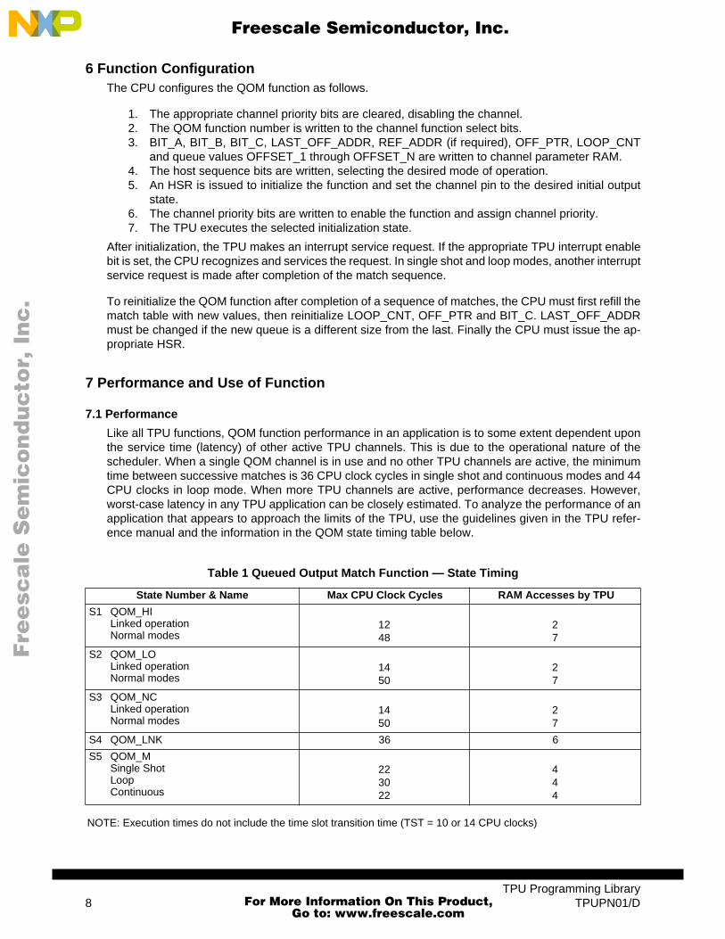
Like all TPU functions, QOM function performance in an application is to some extent dependent uponthe service time (latency) of other active TPU channels. This is due to the operational nature of thescheduler. When a single QOM channel is in use and no other TPU channels are active, the minimumtime between successive matches is 36 CPU clock cycles in single shot and continuous modes and 44CPU clocks in loop mode. When more TPU channels are active, performance decreases. However,worst-case latency in any TPU application can be closely estimated. To analyze the performance of anapplication that appears to approach the limits of the TPU, use the guidelines given in the TPU refer-ence manual and the information in the QOM state timing table below.
NOTE: Execution times do not include the time slot transition time (TST = 10 or 14 CPU clocks)
Table 1 Queued Output Match Function — State Timing
State Number & Name Max CPU Clock Cycles RAM Accesses by TPU
S1 QOM_HILinked operationNormal modes
1248
27
S2 QOM_LOLinked operationNormal modes
1450
27
S3 QOM_NCLinked operationNormal modes
1450
27
S4 QOM_LNK 36 6
S5 QOM_MSingle ShotLoopContinuous
223022
444
TPU Programming Library8 TPUPN01/D
For More Information On This Product,
Go to: www.freescale.com
Fre
esc
ale
Se
mic
on
du
cto
r, I
Freescale Semiconductor, Inc.n
c..
.
7.2 Using Qom for Pulse-Width Modulation
The QOM function can be used to generate a pulse-width modulated output in systems that do not havea dedicated TPU PWM function. A PWM output is generated using continuous mode and two matchoffsets. One offset is configured to generate a rising edge, and the other is configured to generate afalling edge. The offset that generates the rising edge is the low-time parameter and the offset that gen-erates the falling edge is the high-time parameter. Modulation is achieved by varying the offset valuesin the queue. Example D shows PWM setup and output. 100% and 0% duty cycles are easily obtainedby configuring both offsets to generate either a rising edge (100% duty cycle) or a falling edge (0%).
7.3 Initialization to First Match Delay
When an immediate TCR value is used as a reference for the first queued match time, there is a delaybetween the time that the channel pin is initialized and the time that the TCR is read. This delay iscaused by TPU code execution during states 1 and 2. The delay causes the period between pin initial-ization and the output caused by the first match event to be longer than the period specified by the offsetvalue in the first queue entry. The additional time is equivalent to 16 CPU clocks when TCR1 is the timebase and 18 CPU clocks when TCR2 is the time base. If the duration of the initial pin state is critical, itmay be necessary to take this additional time into account when the first offset value is specified.
7.4 Linked Operation
During linked operation, if an additional link is received after the function has started scheduling match-es, state 5 (QOM_LNK) is re-executed. Executing state 5 again causes OFF_PTR to be reset to thestart of the queue, and thus restarts the match sequence. When this happens, any pending match isreplaced by a new scheduled match that is OFFSET_1 counts from the last match event. If an additionallink is received while a loop is executing, the sequence repeats, but LOOP_CNT is not reset to the initialvalue. When a complete match sequence has been executed and the function has stopped, additionallink requests are ignored.
7.5 Changing Mode
The host sequence bits are used to select QOM function operating mode. Change host sequence bitvalues only when the function is stopped or disabled (channel priority bits =%00). Disabling the channelbefore changing mode avoids conditions that cause indeterminate operation, such as selecting loopmode without initializing the LOOP_CNT parameter.
7.6 Using the REF_ADDR Parameter
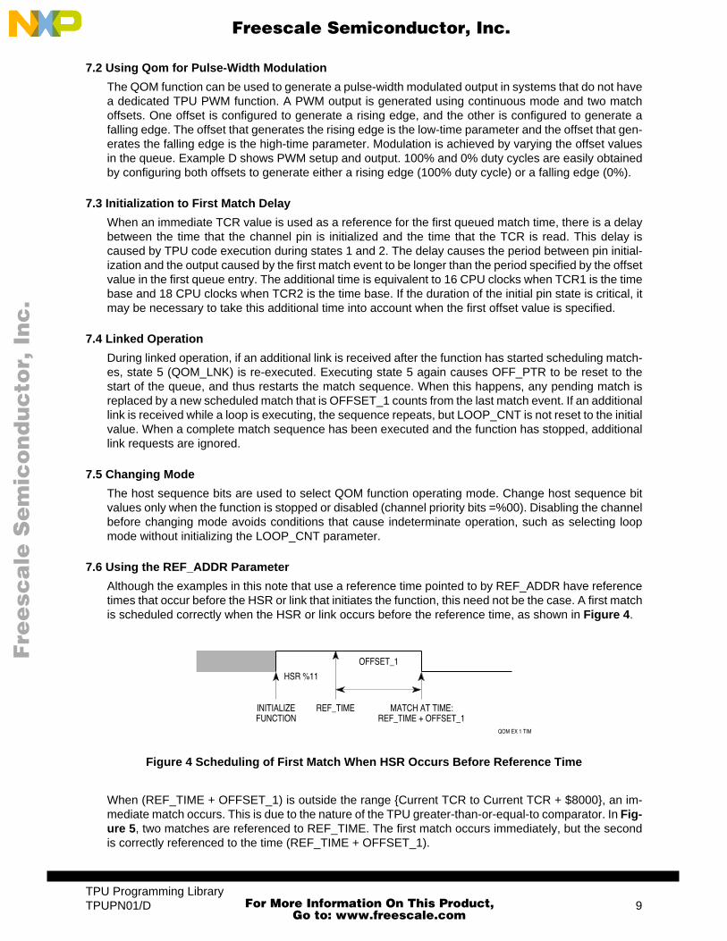
Although the examples in this note that use a reference time pointed to by REF_ADDR have referencetimes that occur before the HSR or link that initiates the function, this need not be the case. A first matchis scheduled correctly when the HSR or link occurs before the reference time, as shown in Figure 4.
Figure 4 Scheduling of First Match When HSR Occurs Before Reference Time
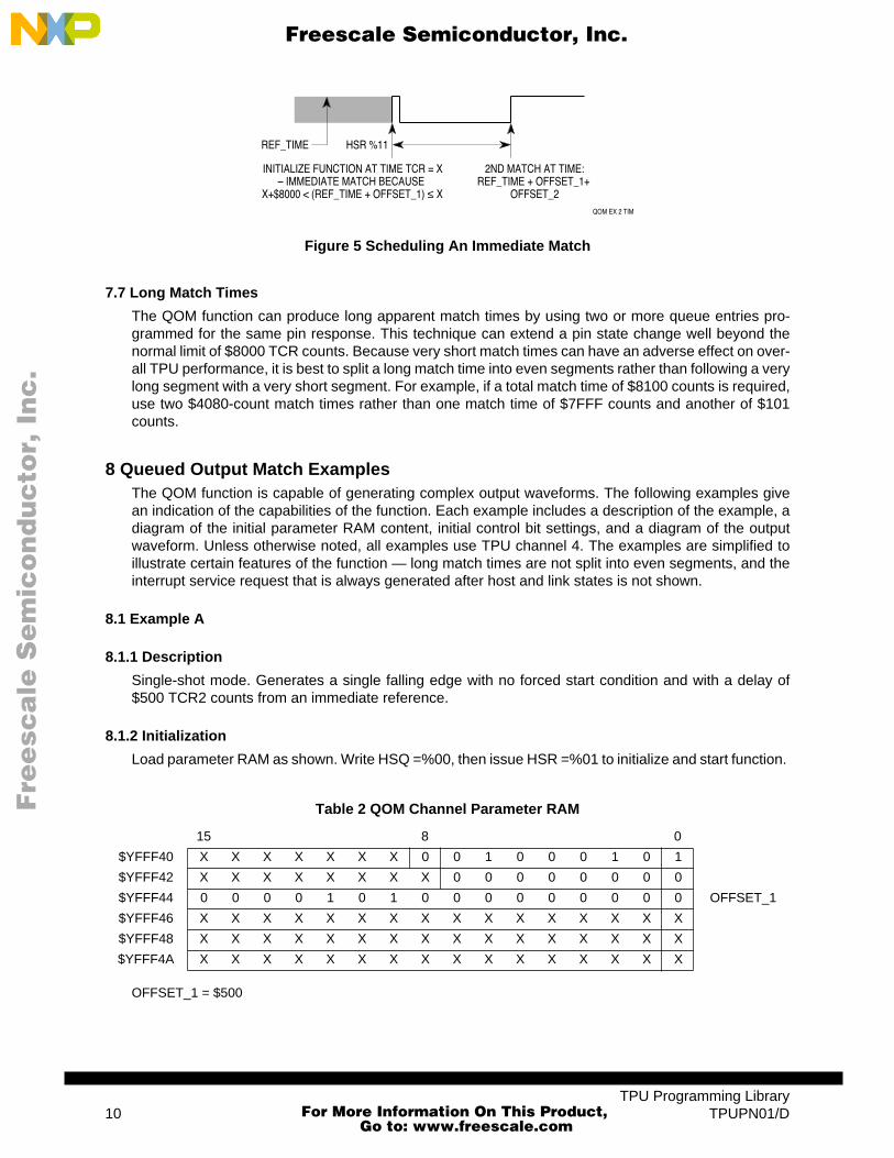
When (REF_TIME + OFFSET_1) is outside the range {Current TCR to Current TCR + $8000}, an im-mediate match occurs. This is due to the nature of the TPU greater-than-or-equal-to comparator. In Fig-ure 5, two matches are referenced to REF_TIME. The first match occurs immediately, but the secondis correctly referenced to the time (REF_TIME + OFFSET_1).
HSR %11
REF_TIME MATCH AT TIME:REF_TIME + OFFSET_1
INITIALIZEFUNCTION
QOM EX 1 TIM
OFFSET_1
TPU Programming LibraryTPUPN01/D 9
For More Information On This Product,
Go to: www.freescale.com
Fre
esc
ale
Se
mic
on
du
cto
r, I
Freescale Semiconductor, Inc.n
c..
.
Figure 5 Scheduling An Immediate Match
7.7 Long Match Times
The QOM function can produce long apparent match times by using two or more queue entries pro-grammed for the same pin response. This technique can extend a pin state change well beyond thenormal limit of $8000 TCR counts. Because very short match times can have an adverse effect on over-all TPU performance, it is best to split a long match time into even segments rather than following a verylong segment with a very short segment. For example, if a total match time of $8100 counts is required,use two $4080-count match times rather than one match time of $7FFF counts and another of $101counts.
8 Queued Output Match ExamplesThe QOM function is capable of generating complex output waveforms. The following examples givean indication of the capabilities of the function. Each example includes a description of the example, adiagram of the initial parameter RAM content, initial control bit settings, and a diagram of the outputwaveform. Unless otherwise noted, all examples use TPU channel 4. The examples are simplified toillustrate certain features of the function — long match times are not split into even segments, and theinterrupt service request that is always generated after host and link states is not shown.
8.1 Example A
8.1.1 Description
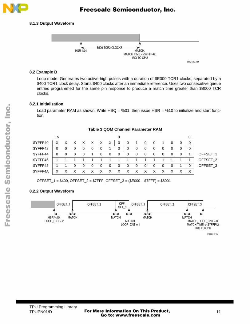
Single-shot mode. Generates a single falling edge with no forced start condition and with a delay of$500 TCR2 counts from an immediate reference.
8.1.2 Initialization
Load parameter RAM as shown. Write HSQ =%00, then issue HSR =%01 to initialize and start function.
OFFSET_1 = $500
Table 2 QOM Channel Parameter RAM
15 8 0
$YFFF40 X X X X X X X 0 0 1 0 0 0 1 0 1
$YFFF42 X X X X X X X X 0 0 0 0 0 0 0 0
$YFFF44 0 0 0 0 1 0 1 0 0 0 0 0 0 0 0 0 OFFSET_1
$YFFF46 X X X X X X X X X X X X X X X X
$YFFF48 X X X X X X X X X X X X X X X X
$YFFF4A X X X X X X X X X X X X X X X X
REF_TIME
2ND MATCH AT TIME:REF_TIME + OFFSET_1+
OFFSET_2
INITIALIZE FUNCTION AT TIME TCR = X– IMMEDIATE MATCH BECAUSE
X+$8000 < (REF_TIME + OFFSET_1) ≤ XQOM EX 2 TIM
HSR %11
TPU Programming Library10 TPUPN01/D
For More Information On This Product,
Go to: www.freescale.com
Fre
esc
ale
Se
mic
on
du
cto
r, I
Freescale Semiconductor, Inc.n
c..
.
8.1.3 Output Waveform
8.2 Example B
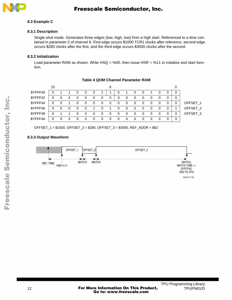
Loop mode. Generates two active-high pulses with a duration of $E000 TCR1 clocks, separated by a$400 TCR1 clock delay. Starts $400 clocks after an immediate reference. Uses two consecutive queueentries programmed for the same pin response to produce a match time greater than $8000 TCRclocks.
8.2.1 Initialization
Load parameter RAM as shown. Write HSQ = %01, then issue HSR = %10 to initialize and start func-tion.
OFFSET_1 = $400, OFFSET_2 = $7FFF, OFFSET_3 = ($E000 – $7FFF) = $6001
8.2.2 Output Waveform
Table 3 QOM Channel Parameter RAM
15 8 0
$YFFF40 X X X X X X X 0 0 1 0 0 1 0 0 0
$YFFF42 0 0 0 0 0 0 1 0 0 0 0 0 0 0 0 0
$YFFF44 0 0 0 0 1 0 0 0 0 0 0 0 0 0 0 1 OFFSET_1
$YFFF46 1 1 1 1 1 1 1 1 1 1 1 1 1 1 1 1 OFFSET_2
$YFFF48 1 1 0 0 0 0 0 0 0 0 0 0 0 0 1 0 OFFSET_3
$YFFF4A X X X X X X X X X X X X X X X X
QOM EX A TIM
HSR %01 MATCH,MATCH TIME -> $YFFF42,
IRQ TO CPU
$500 TCR2 CLOCKS
HSR %10,LOOP_CNT = 2
MATCH MATCHMATCH,
LOOP_CNT = 1
MATCH MATCHMATCH, LOOP_CNT = 0,
MATCH TIME -> $YFFF42,IRQ TO CPU
OFFSET_1 OFFSET_2 OFFSET_1 OFFSET_2 OFFSET_3
QOM EX B TIM
OFF-SET_3
TPU Programming LibraryTPUPN01/D 11
For More Information On This Product,
Go to: www.freescale.com
Fre
esc
ale
Se
mic
on
du
cto
r, I
Freescale Semiconductor, Inc.n
c..
.
8.3 Example C
8.3.1 Description
Single-shot mode. Generates three edges (low, high, low) from a high start. Referenced to a time con-tained in parameter 2 of channel 6. First edge occurs $1000 TCR1 clocks after reference, second edgeoccurs $280 clocks after the first, and the third edge occurs $3000 clocks after the second.
8.3.2 Initialization
Load parameter RAM as shown. Write HSQ = %00, then issue HSR = %11 to initialize and start func-tion.
OFFSET_1 = $1000, OFFSET_2 = $280, OFFSET_3 = $3000, REF_ADDR = $62
8.3.3 Output Waveform
Table 4 QOM Channel Parameter RAM
15 8 0
$YFFF40 0 1 1 0 0 0 1 1 0 1 0 0 1 0 0 0
$YFFF42 X X X X X X X X 0 0 0 0 0 0 0 0
$YFFF44 0 0 1 0 0 0 0 0 0 0 0 0 0 0 0 0 OFFSET_1
$YFFF46 0 0 0 0 0 1 0 1 0 0 0 0 0 0 0 1 OFFSET_2
$YFFF48 0 1 1 0 0 0 0 0 0 0 0 0 0 0 0 0 OFFSET_3
$YFFF4A X X X X X X X X X X X X X X X X
HSR %11REF_TIME
OFFSET_1 OFFSET_2 OFFSET_3
MATCH MATCH MATCH,MATCH TIME ->
$YFFF42,IRQ TO CPU
QOM EX C TIM
TPU Programming Library12 TPUPN01/D
For More Information On This Product,
Go to: www.freescale.com
Fre
esc
ale
Se
mic
on
du
cto
r, I
Freescale Semiconductor, Inc.n
c..
.
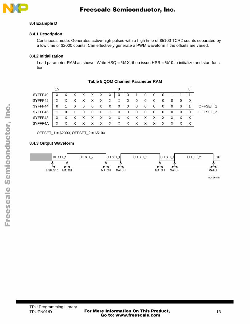
8.4 Example D
8.4.1 Description
Continuous mode. Generates active-high pulses with a high time of $5100 TCR2 counts separated bya low time of $2000 counts. Can effectively generate a PWM waveform if the offsets are varied.
8.4.2 Initialization
Load parameter RAM as shown. Write HSQ = %1X, then issue HSR = %10 to initialize and start func-tion.
OFFSET_1 = $2000, OFFSET_2 = $5100
8.4.3 Output Waveform
Table 5 QOM Channel Parameter RAM
15 8 0
$YFFF40 X X X X X X X 0 0 1 0 0 0 1 1 1
$YFFF42 X X X X X X X X 0 0 0 0 0 0 0 0
$YFFF44 0 1 0 0 0 0 0 0 0 0 0 0 0 0 0 1 OFFSET_1
$YFFF46 1 0 1 0 0 0 1 0 0 0 0 0 0 0 0 0 OFFSET_2
$YFFF48 X X X X X X X X X X X X X X X X
$YFFF4A X X X X X X X X X X X X X X X X
HSR %10
OFFSET_1 OFFSET_2 OFFSET_1 OFFSET_2 OFFSET_1 OFFSET_2 ETC
MATCH MATCH MATCH MATCH MATCH MATCH
QOM EX D TIM
TPU Programming LibraryTPUPN01/D 13
For More Information On This Product,
Go to: www.freescale.com
Fre
esc
ale
Se
mic
on
du
cto
r, I
Freescale Semiconductor, Inc.n
c..
.
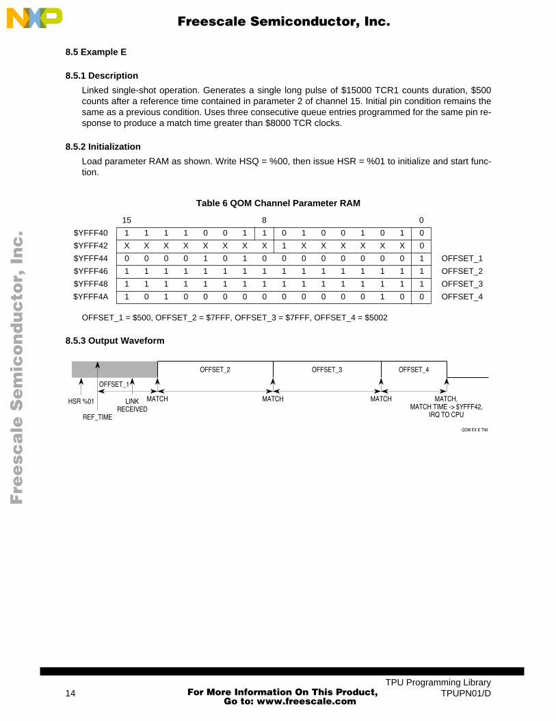
8.5 Example E
8.5.1 Description
Linked single-shot operation. Generates a single long pulse of $15000 TCR1 counts duration, $500counts after a reference time contained in parameter 2 of channel 15. Initial pin condition remains thesame as a previous condition. Uses three consecutive queue entries programmed for the same pin re-sponse to produce a match time greater than $8000 TCR clocks.
8.5.2 Initialization
Load parameter RAM as shown. Write HSQ = %00, then issue HSR = %01 to initialize and start func-tion.
OFFSET_1 = $500, OFFSET_2 = $7FFF, OFFSET_3 = $7FFF, OFFSET_4 = $5002
8.5.3 Output Waveform
Table 6 QOM Channel Parameter RAM
15 8 0
$YFFF40 1 1 1 1 0 0 1 1 0 1 0 0 1 0 1 0
$YFFF42 X X X X X X X X 1 X X X X X X 0
$YFFF44 0 0 0 0 1 0 1 0 0 0 0 0 0 0 0 1 OFFSET_1
$YFFF46 1 1 1 1 1 1 1 1 1 1 1 1 1 1 1 1 OFFSET_2
$YFFF48 1 1 1 1 1 1 1 1 1 1 1 1 1 1 1 1 OFFSET_3
$YFFF4A 1 0 1 0 0 0 0 0 0 0 0 0 0 1 0 0 OFFSET_4
HSR %01 LINKRECEIVED
REF_TIME
MATCH MATCH MATCH MATCH,MATCH TIME -> $YFFF42,
IRQ TO CPU
OFFSET_1
OFFSET_2 OFFSET_3 OFFSET_4
QOM EX E TIM
TPU Programming Library14 TPUPN01/D
For More Information On This Product,
Go to: www.freescale.com
Fre
esc
ale
Se
mic
on
du
cto
r, I
Freescale Semiconductor, Inc.n
c..
.
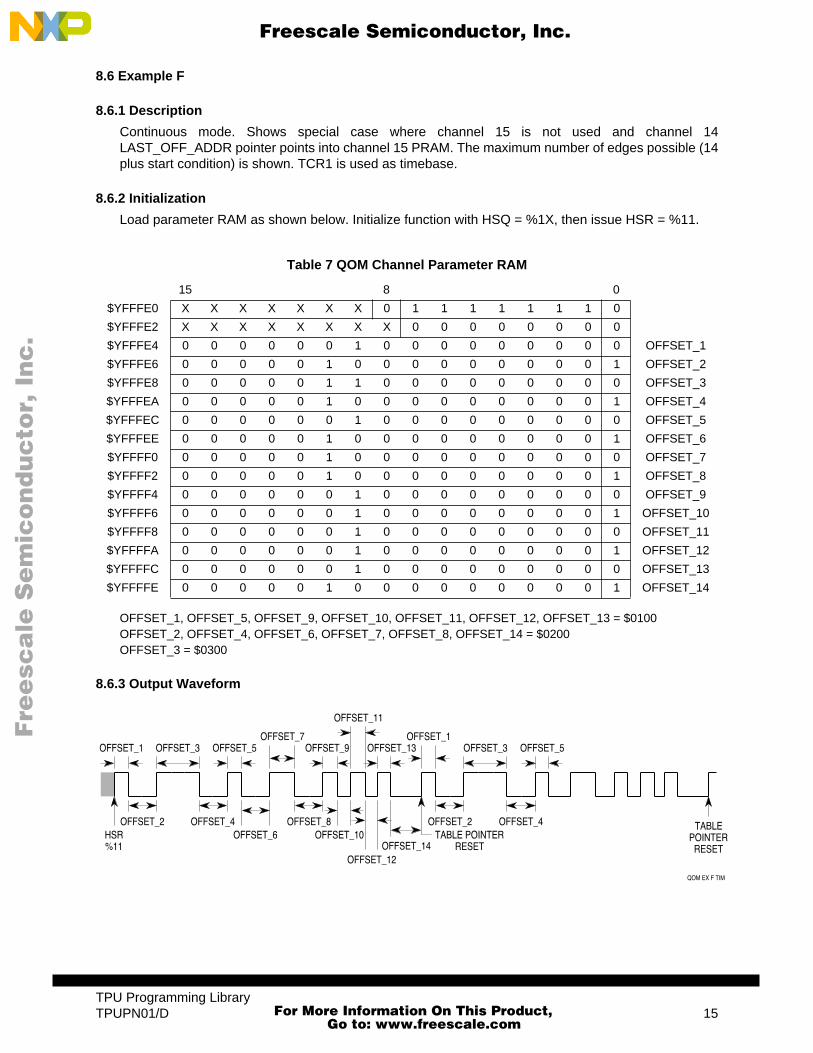
8.6 Example F
8.6.1 Description
Continuous mode. Shows special case where channel 15 is not used and channel 14LAST_OFF_ADDR pointer points into channel 15 PRAM. The maximum number of edges possible (14plus start condition) is shown. TCR1 is used as timebase.
8.6.2 Initialization
Load parameter RAM as shown below. Initialize function with HSQ = %1X, then issue HSR = %11.
OFFSET_1, OFFSET_5, OFFSET_9, OFFSET_10, OFFSET_11, OFFSET_12, OFFSET_13 = $0100OFFSET_2, OFFSET_4, OFFSET_6, OFFSET_7, OFFSET_8, OFFSET_14 = $0200OFFSET_3 = $0300
8.6.3 Output Waveform
Table 7 QOM Channel Parameter RAM
15 8 0
$YFFFE0 X X X X X X X 0 1 1 1 1 1 1 1 0
$YFFFE2 X X X X X X X X 0 0 0 0 0 0 0 0
$YFFFE4 0 0 0 0 0 0 1 0 0 0 0 0 0 0 0 0 OFFSET_1
$YFFFE6 0 0 0 0 0 1 0 0 0 0 0 0 0 0 0 1 OFFSET_2
$YFFFE8 0 0 0 0 0 1 1 0 0 0 0 0 0 0 0 0 OFFSET_3
$YFFFEA 0 0 0 0 0 1 0 0 0 0 0 0 0 0 0 1 OFFSET_4
$YFFFEC 0 0 0 0 0 0 1 0 0 0 0 0 0 0 0 0 OFFSET_5
$YFFFEE 0 0 0 0 0 1 0 0 0 0 0 0 0 0 0 1 OFFSET_6
$YFFFF0 0 0 0 0 0 1 0 0 0 0 0 0 0 0 0 0 OFFSET_7
$YFFFF2 0 0 0 0 0 1 0 0 0 0 0 0 0 0 0 1 OFFSET_8
$YFFFF4 0 0 0 0 0 0 1 0 0 0 0 0 0 0 0 0 OFFSET_9
$YFFFF6 0 0 0 0 0 0 1 0 0 0 0 0 0 0 0 1 OFFSET_10
$YFFFF8 0 0 0 0 0 0 1 0 0 0 0 0 0 0 0 0 OFFSET_11
$YFFFFA 0 0 0 0 0 0 1 0 0 0 0 0 0 0 0 1 OFFSET_12
$YFFFFC 0 0 0 0 0 0 1 0 0 0 0 0 0 0 0 0 OFFSET_13
$YFFFFE 0 0 0 0 0 1 0 0 0 0 0 0 0 0 0 1 OFFSET_14
OFFSET_1
HSR%11
OFFSET_2
OFFSET_3
OFFSET_4
OFFSET_5
OFFSET_6
OFFSET_7
OFFSET_8
OFFSET_9
OFFSET_10
OFFSET_11
OFFSET_12
OFFSET_13
OFFSET_14
OFFSET_1
OFFSET_2
OFFSET_3
OFFSET_4
OFFSET_5
TABLE
RESETTABLE POINTER
RESET
QOM EX F TIM
POINTER
TPU Programming LibraryTPUPN01/D 15
For More Information On This Product,
Go to: www.freescale.com
Fre
esc
ale
Se
mic
on
du
cto
r, I
Freescale Semiconductor, Inc.n
c..
.
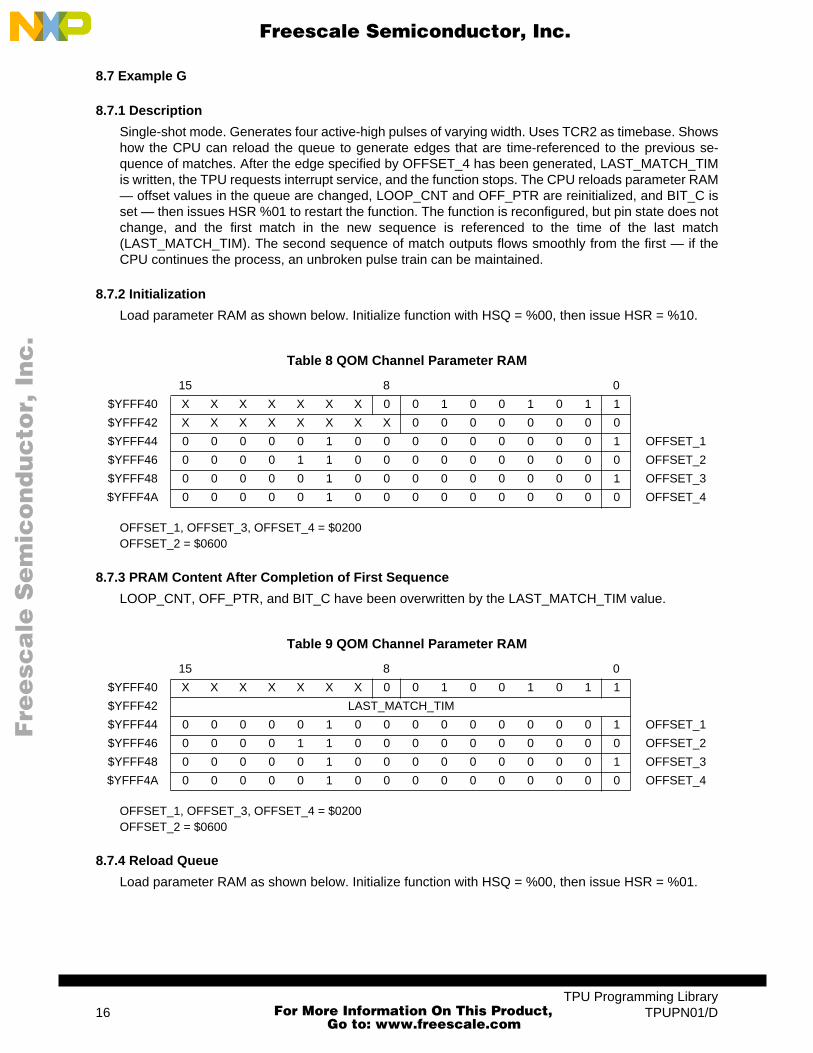
8.7 Example G
8.7.1 Description
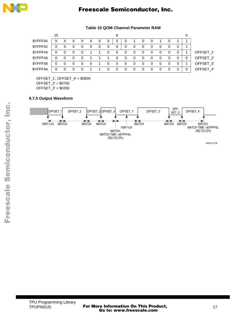
Single-shot mode. Generates four active-high pulses of varying width. Uses TCR2 as timebase. Showshow the CPU can reload the queue to generate edges that are time-referenced to the previous se-quence of matches. After the edge specified by OFFSET_4 has been generated, LAST_MATCH_TIMis written, the TPU requests interrupt service, and the function stops. The CPU reloads parameter RAM— offset values in the queue are changed, LOOP_CNT and OFF_PTR are reinitialized, and BIT_C isset — then issues HSR %01 to restart the function. The function is reconfigured, but pin state does notchange, and the first match in the new sequence is referenced to the time of the last match(LAST_MATCH_TIM). The second sequence of match outputs flows smoothly from the first — if theCPU continues the process, an unbroken pulse train can be maintained.
8.7.2 Initialization
Load parameter RAM as shown below. Initialize function with HSQ = %00, then issue HSR = %10.
OFFSET_1, OFFSET_3, OFFSET_4 = $0200OFFSET_2 = $0600
8.7.3 PRAM Content After Completion of First Sequence
LOOP_CNT, OFF_PTR, and BIT_C have been overwritten by the LAST_MATCH_TIM value.
OFFSET_1, OFFSET_3, OFFSET_4 = $0200OFFSET_2 = $0600
8.7.4 Reload Queue
Load parameter RAM as shown below. Initialize function with HSQ = %00, then issue HSR = %01.
Table 8 QOM Channel Parameter RAM
15 8 0
$YFFF40 X X X X X X X 0 0 1 0 0 1 0 1 1
$YFFF42 X X X X X X X X 0 0 0 0 0 0 0 0
$YFFF44 0 0 0 0 0 1 0 0 0 0 0 0 0 0 0 1 OFFSET_1
$YFFF46 0 0 0 0 1 1 0 0 0 0 0 0 0 0 0 0 OFFSET_2
$YFFF48 0 0 0 0 0 1 0 0 0 0 0 0 0 0 0 1 OFFSET_3
$YFFF4A 0 0 0 0 0 1 0 0 0 0 0 0 0 0 0 0 OFFSET_4
Table 9 QOM Channel Parameter RAM
15 8 0
$YFFF40 X X X X X X X 0 0 1 0 0 1 0 1 1
$YFFF42 LAST_MATCH_TIM
$YFFF44 0 0 0 0 0 1 0 0 0 0 0 0 0 0 0 1 OFFSET_1
$YFFF46 0 0 0 0 1 1 0 0 0 0 0 0 0 0 0 0 OFFSET_2
$YFFF48 0 0 0 0 0 1 0 0 0 0 0 0 0 0 0 1 OFFSET_3
$YFFF4A 0 0 0 0 0 1 0 0 0 0 0 0 0 0 0 0 OFFSET_4
TPU Programming Library16 TPUPN01/D
For More Information On This Product,
Go to: www.freescale.com
F
ree
sca
le S
em
ico
nd
uc
tor,
I
Freescale Semiconductor, Inc.n
c..
.
OFFSET_1', OFFSET_4' = $0600OFFSET_2' = $0700OFFSET_3' = $0200
8.7.5 Output Waveform
Table 10 QOM Channel Parameter RAM
15 8 0
$YFFF40 X X X X X X X 0 0 1 0 0 1 0 1 1
$YFFF42 X X X X X X X X 0 0 0 0 0 0 0 1
$YFFF44 0 0 0 0 1 1 0 0 0 0 0 0 0 0 0 1 OFFSET_1'
$YFFF46 0 0 0 0 1 1 1 0 0 0 0 0 0 0 0 0 OFFSET_2'
$YFFF48 0 0 0 0 0 1 0 0 0 0 0 0 0 0 0 1 OFFSET_3'
$YFFF4A 0 0 0 0 1 1 0 0 0 0 0 0 0 0 0 0 OFFSET_4'
HSR %10
OFFSET_1 OFFSET_2 OFFSET_3 OFFSET_4 OFFSET_1' OFFSET_2'
MATCH MATCH MATCH
MATCH,MATCH TIME ->$YFFF42,
IRQ TO CPU
MATCH MATCH MATCH
OFF-OFFSET_4'
HSR %01MATCH,
MATCH TIME ->$YFFF42,IRQ TO CPU
QOM EX G TIM
SET_3'
TPU Programming LibraryTPUPN01/D 17
For More Information On This Product,
Go to: www.freescale.com
F
ree
sca
le S
em
ico
nd
uc
tor,
I
Freescale Semiconductor, Inc.n
c..
.
9 Queued Output Match AlgorithmThe following description is provided as a guide only, to aid understanding of the function. The exactsequence of operations in microcode may be different to optimize speed and code size. TPU microcodesource listings for all functions in the TPU function library can be downloaded from the Freescale Free-ware bulletin board. Refer to Using the TPU Function Library and TPU Emulation Mode (TPUPN00/D)for detailed instructions on downloading and compiling microcode.
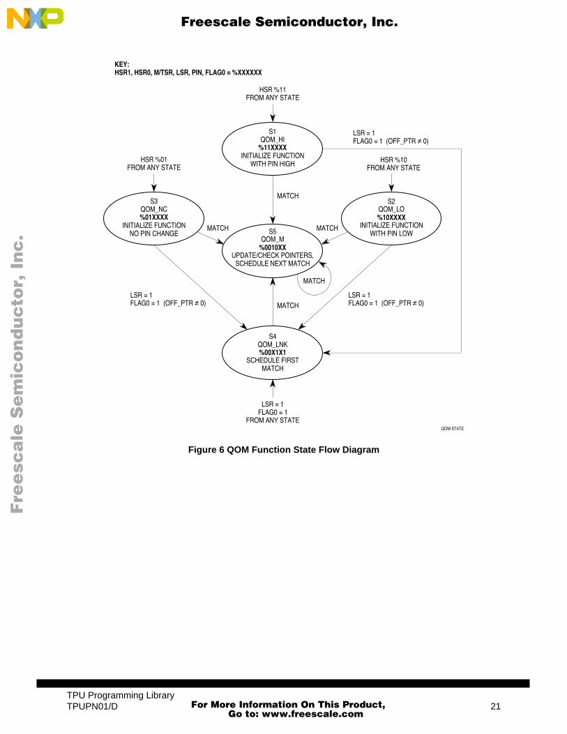
The queued output match function consists of five states, which are described below. In the state de-scriptions, the phrases ‘last match time’ and ‘last event time’ refer to two different things. Match time isthe value that is loaded into the match register. Event time is the value that is captured when a matchoccurs. In almost all cases, these values are the same. However, when a match register update resultsin an immediate match, the values differ. For example, if the current TCR value is $6000 and $5E00 iswritten into the match register, an immediate match occurs. Subsequently, ‘last match time’ is $5E00,but ‘last event time’ is $6000. Figure 6, which follows the state descriptions, is a state flow diagram ofthe QOM function. For clarity, reference is made to internal channel flags 0 and 1 in the following de-scription. These are internal TPU control bits that are not available to the user.
9.1 STATE1 —QOM_HIThis state, entered as a result of HSR 11, performs initialization of the QOM function.
The channel pin is configured as an outputThe pin state set high. BIT_C is tested
If BIT_C = 0An immediate match is generated and cleared to cancel any pending matchFlag1 is cleared
If BIT_C = 1Flag1 is set
BIT_A is tested to determine the timebase for the match sequenceIf BIT_A = 0
TCR1 is selectedIf BIT_A = 1
TCR2 is selectedOFF_PTR is tested
If OFF_PTR ≠ 0Link mode is selectedChannel flag0 is setThe TPU requests interrupt service from the CPUThe state ends
If OFF_PTR = 0Channel flag0 is clearedThe first match is scheduled
OFF_PTR is initialized to point to OFFSET_1 (this overwrites BIT_C)BIT_B and flag1 (BIT_C) are tested to determine reference time
%00 = Immediate TCR%X1 = Last Event Time%10 = Value pointed to by REF_ADDR
OFFSET_1 is right-shifted The selected reference time is added to the shifted offset valueThe sum is written to the match registerThe value of OFFSET_1 bit0 is used to determine pin response to the scheduled match
The TPU requests interrupt service from the CPUThe state ends.
TPU Programming Library18 TPUPN01/D
For More Information On This Product,
Go to: www.freescale.com
F
ree
sca
le S
em
ico
nd
uc
tor,
I
Freescale Semiconductor, Inc.n
c..
.
9.2 STATE2 —QOM_LO
This state is entered as a result of HSR 10. It is identical to STATE1 except that initial pin state is low.
9.3 STATE3 — QOM_NC
This state is entered as a result of HSR 01. It is identical to STATE1 except that initial pin state is un-changed from the previous state. Because STATE3 continues a previously-defined initial pin state, HSR11 should not be used to initiate QOM operation unless it has been preceded by at least one sequenceinitiated by either HSR 01 or HSR 10.
9.4 STATE4 — QOM_LNK
STATE4 is entered in response to a link request from another TPU channel as long as channel flag0 isset.
BIT_A is tested to determine the timebase for the match sequenceIf BIT_A = 0
TCR1 is selectedIf BIT_A = 1
TCR2 is selectedThe first match is scheduled
OFF_PTR is initialized to point to OFFSET_1 (this overwrites BIT_C)BIT_B and flag1 (BIT_C) are tested to determine reference time
%00 = Immediate TCR%X1 = Last Event Time%10 = Value pointed to by REF_ADDR
OFFSET_1 is right-shifted one placeThe selected reference time is added to the shifted offset valueThe sum is written to the match registerThe value of OFFSET_1 bit0 is used to determine pin response to the scheduled match The TPU requests interrupt service from the CPUThe state ends.
9.5 STATE5 — QOM_M
This state is entered as a result of a match event on the QOM channel. Operation differs depending onthe mode selected:
9.6 Single-Shot ModeQueue pointer OFF_PTR is compared to LAST_OFF_ADDR
If OFF_PTR = LAST_OFF_ADDR The last event time is stored in LAST_MATCH_TIM, overwriting LOOP_CNT and OFF_PTR.The TPU requests interrupt service from the CPUThe state ends.
If OFF_PTR ≠ LAST_OFF_ADDR OFF_PTR is incremented by 2 (word access) The incremented OFF_PTR value is used to obtain the next match offset from the tableA new match is scheduled
The new offset value is right-shifted one placeThe shifted offset value is added to the last match timeThe sum is written to the match registerBit0 of the offset parameter is used to determine pin response to the match
The state ends.
TPU Programming LibraryTPUPN01/D 19
For More Information On This Product,
Go to: www.freescale.com
F
ree
sca
le S
em
ico
nd
uc
tor,
I
Freescale Semiconductor, Inc.n
c..
.
9.7 Loop ModeQueue pointer OFF_PTR is compared to LAST_OFF_ADDR
If OFF_PTR = LAST_OFF_ADDR OFF_PTR is reinitialized to point to OFFSET_1LOOP_CNT is decremented.LOOP_CNT is tested
If LOOP_CNT = 0The last event time is stored in LAST_MATCH_TIM, overwriting LOOP_CNT and OFF_PTR. The TPU requests interrupt service from the CPUThe state ends.
If LOOP_CNT ≠ 0A new match is scheduled
The OFFSET_1 value is right-shifted one placeThe shifted offset value is added to the last match timeThe sum is written to the match registerBit0 of the OFFSET_1 parameter is used to determine pin response to the match
The state ends. If OFF_PTR ≠ LAST_OFF_ADDR
OFF_PTR is incremented by 2 (word access) The incremented OFF_PTR value is used to obtain the next match offset from the queueA new match is scheduled
The new offset value is right-shifted The shifted offset value is added to the previous match timeThe sum of match time and shifted offset value is written to the match registerBit0 of the offset parameter is used to determine pin response to the scheduled match
The state ends.
9.8 Continuous ModeQueue pointer OFF_PTR is compared to LAST_OFF_ADDR
If OFF_PTR = LAST_OFF_ADDR OFF_PTR is reinitialized to point to OFFSET_1A new match is scheduled
The OFFSET_1 value is right-shifted one placeThe shifted offset value is added to the last match timeThe sum is written to the match registerBit0 of the OFFSET_1 parameter is used to determine pin response to the scheduled match
The state ends. If OFF_PTR ≠ LAST_OFF_ADDR
OFF_PTR is incremented by 2 (word access) The incremented OFF_PTR value is used to obtain the next match offset from the queueA new match is scheduled
The new offset value is right-shifted The shifted offset value is added to the previous match timeThe sum of match time and shifted offset value is written to the match registerBit0 of the offset parameter is used to determine pin response to the scheduled match
The state ends.
TPU Programming Library20 TPUPN01/D
For More Information On This Product,
Go to: www.freescale.com
F
ree
sca
le S
em
ico
nd
uc
tor,
I
Freescale Semiconductor, Inc.n
c..
.
Figure 6 QOM Function State Flow Diagram
KEY:HSR1, HSR0, M/TSR, LSR, PIN, FLAG0 = %XXXXXX
LSR = 1FLAG0 = 1
FROM ANY STATE
S1QOM_HI
INITIALIZE FUNCTIONWITH PIN HIGH
S5QOM_M
UPDATE/CHECK POINTERS,SCHEDULE NEXT MATCH
HSR %11FROM ANY STATE
LSR = 1FLAG0 = 1 (OFF_PTR ≠ 0)
LSR = 1FLAG0 = 1 (OFF_PTR ≠ 0)
LSR = 1FLAG0 = 1 (OFF_PTR ≠ 0)
MATCH
MATCHMATCH
MATCH
%11XXXX
HSR %10FROM ANY STATE
S2QOM_LO
INITIALIZE FUNCTIONWITH PIN LOW
%10XXXX
S3QOM_NC
INITIALIZE FUNCTIONNO PIN CHANGE
HSR %01FROM ANY STATE
%01XXXX
S4QOM_LNK
SCHEDULE FIRSTMATCH
%00X1X1
%0010XX
MATCH
QOM STATE
TPU Programming LibraryTPUPN01/D 21
For More Information On This Product,
Go to: www.freescale.com
F
ree
sca
le S
em
ico
nd
uc
tor,
I
Freescale Semiconductor, Inc.n
c..
.
NOTES
TPU Programming Library22 TPUPN01/D
For More Information On This Product,
Go to: www.freescale.com
F
ree
sca
le S
em
ico
nd
uc
tor,
I
Freescale Semiconductor, Inc.n
c..
.
NOTES
TPU Programming LibraryTPUPN01/D 23
For More Information On This Product,
Go to: www.freescale.com
F
ree
sca
le S
em
ico
nd
uc
tor,
I
Freescale Semiconductor, Inc.n
c..
.
For More Information On This Product,
Go to: www.freescale.com