quantum memory management systems - nwcl.ku.edu.tr · quantum memory management systems caglar koca...
TRANSCRIPT
Quantum Memory Management Systems
Caglar KocaNext-generation and Wireless Communications
LaboratoryKoc University
Istanbul, [email protected]
Ozgur B. AkanNext-generation and Wireless Communications
LaboratoryKoc University
Istanbul, [email protected]
ABSTRACTQuantum computation is a developing area in science. Ow-ing to the new developments in nanotechnology, some prac-tical quantum computing applications are emerging. Eventhough quantum computation possesses many inherent su-periorities, it su↵er from a tight bottleneck: Quantum Stor-age. In this paper, we identify properties of a good quantumstorage unit and propose unique quantum memory struc-tures and discuss them in terms of circuit complexity, ac-cess delay complexity, maximum connectivity and ancillaryqubits required. We reveal that quantum teleportation pro-vide advantage only in maximum connectivity among theproperties we analyzed.
Categories and Subject DescriptorsB.10.10 [Quantum Technologies]: Quantum Computa-tion; C.1.4 [Other Architectures]: Quantum Comput-ing—complexity measures, performance measures
General TermsQuantum Information
KeywordsQuantum communication, quantum computation, quantumstorage, teleportation, swap
1. INTRODUCTIONEver since Feynman hinted the quantum computing in
1982, a long way has been covered to turn this dream intoreality. A number of quantum algorithms have revolution-ized many fields of computing, especially in Searching [2]and Factoring [7]. Some quantum processor units [6, 1] andquantum arithmetic logic unit structures have been devel-oped [9, 10] and some of them are engineered [10]. Somememory structures are also theorized [3], and thanks to therecent developments in nanotechnology, small sized quantum
Permission to make digital or hard copies of all or part of this work for
personal or classroom use is granted without fee provided that copies are not
made or distributed for profit or commercial advantage and that copies bear
this notice and the full citation on the first page. Copyrights for components
of this work owned by others than ACM must be honored. Abstracting with
credit is permitted. To copy otherwise, or republish, to post on servers or to
redistribute to lists, requires prior specific permission and/or a fee. Request
permissions from [email protected].
NANOCOM’15, September 21 - 22, 2015, Boston, MA, USA
c�2015 ACM 978-1-4503-3674-1/15/09 ...$15.00.
http://dx.doi.org/10.1145/2800795.2800810.
memory systems has been built [8]. However, to the best ofour knowledge, no quantum memory management systemfeasible for large memory contents have been suggested.
Classical memory systems use finite number of buses toaccess a memory location. The desired memory locationcan be activated by various methods using encoders or mul-tiplexers, while the other memory cells are kept at a highimpedance state. The desired content may reach any placefrom the bus as it is not a↵ected by other memory cells.
Due to the lack of high impedance gates for quantumstates, quantum memory cells cannot be accessed directlyby their addresses. In fact, there are two mechanisms whichmay transport qubits from one location to another: Swap-ping and teleportation [4].
For a memory consisting of N qubits, complexity of reach-ing the desired content is obviously O(N) which renders un-organized swapping impractical. Teleportation itself cannotbe a solution as well, there has to be another search at thetarget location of the qubit. Moreover, the EPR pairs arealso qubits and they somehow have to be distributed to theteleportation zones. Note that sending EPR pairs are nodi↵erent than retriving qubits. In both cases, a qubit istransferred from a target to a destination.
The rest of the paper is organized as follows. In the sec-tion II, we introduce the features of a quantum memorymanagement system. In Section III, we explain and analyzepossible one-staged memory management systems using onlyswapping. In Section IV, we deepen our analysis to multi-layered memory management architectures. In Section V,we employ teleportation as well as swapping for memorymanagement. We compare the suggested systems in SectionVI. Section VII is conclusion.
2. QUANTUM MEMORY MANAGEMENTSYSTEMS
We suggest that a quantum memory management systemhas four main properties:
1. Access Delay Complexity
2. Circuit Complexity
3. Maximum Connectivity
4. Ancillary Qubits
Access delay complexity, ADC, is how access time in-creases as the memory size increases. ADC a↵ects the over-all speed of the system. Circuit complexity, CC, is how thenumber of gates required to access a memory location in-creases as the memory size increases. CC is related to the
circuit size, cost of the system and feasibility. MaximumConnectivity, MC, is the most number of gates connectedto a qubit. MC is a concept close to fan-out in classicalcircuits. Ancillary Qubits, AQ, are the number of qubitsrequired to reach a memory location. These qubits are usedin qubit teleportation, as we need an EPR pair to achieveteleportation. Note that MC and AQ give us direct valuesrather than complexities.
It is clear that all of these quantities should be small fora memory management system to be feasible. Below, wewill explain and analyze the possible memory architectureswith their access delay complexities, circuit complexities,maximum connectivity and ancillary qubit numbers.
3. ONE LAYERED ARCHITECTURES WITHONLY SWAPPING
In this chapter, we discuss the possible architectures fora one layered memory management system. These archi-tectures may not be feasible for large memories but theymay constitute building blocks for larger memory structures.Note that we use Fredkin Gates [4] which have been phys-ically realized and can be used to construct the suggestedschemes. [11].
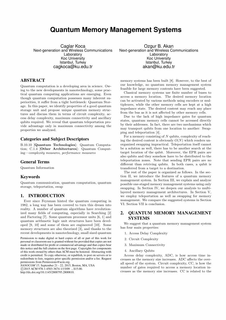
3.1 Simple SwappingSimple Swapping is basically to swap each qubit until the
target qubit reachs its destination. A simple swapping cir-cuit is depicted on Figure 1. It is obvious that the circuitcomplexity of Swapping is O(N), as it requires N FredkinGates. The access delay complexity is also N , due to thefact that, on average, we need to swap the memory contentN
2
times. Its maximum connectivity is 2, as each qubit isconnected to two gates. Due to the large amount of delay,we can say that simple swapping is not a feasible suggestionfor fast access for large blocks. Note that output can betaken via any quantum wire.
Figure 1: Simple Swapping Circuit.
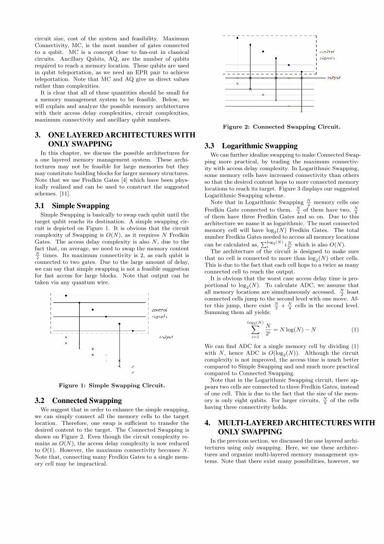
3.2 Connected SwappingWe suggest that in order to enhance the simple swapping,
we can simply connect all the memory cells to the targetlocation. Therefore, one swap is su�cient to transfer thedesired content to the target. The Connected Swapping isshown on Figure 2. Even though the circuit complexity re-mains as O(N), the access delay complexity is now reducedto O(1). However, the maximum connectivity becomes N .Note that, connecting many Fredkin Gates to a single mem-ory cell may be impractical.
Figure 2: Connected Swapping Circuit.
3.3 Logarithmic SwappingWe can further idealize swapping to make Connected Swap-
ping more practical, by trading the maximum connectiv-ity with access delay complexity. In Logarithmic Swapping,some memory cells have increased connectivity than othersso that the desired content hops to more connected memorylocations to reach its target. Figure 3 displays our suggestedLogarithmic Swapping scheme.
Note that in Logarithmic Swapping N
2
memory cells oneFredkin Gate connected to them. N
4
of them have two, N
8
of them have three Fredkin Gates and so on. Due to thisarchitecture we name it as logarithmic. The most connectedmemory cell will have log
2
(N) Fredkin Gates. The totalnumber Fredkin Gates needed to access all memory locations
can be calculated as,P
log2(N)
i
iN2
i which is also O(N).The architecture of the circuit is designed to make sure
that no cell is connected to more than log2
(N) other cells.This is due to the fact that each cell hops to a twice as manyconnected cell to reach the output.
It is obvious that the worst case access delay time is pro-portional to log
2
(N). To calculate ADC, we assume thatall memory locations are simultaneously accessed. N
2
leastconnected cells jump to the second level with one move. Af-ter this jump, there exist N
2
+ N
4
cells in the second level.Summing them all yields:
log2(N)X
i=1
N
2i= N log(N)�N (1)
We can find ADC for a single memory cell by dividing (1)with N , hence ADC is O(log
2
(N)). Although the circuitcomplexity is not improved, the access time is much bettercompared to Simple Swapping and and much more practicalcompared to Connected Swapping.
Note that in the Logarithmic Swapping circuit, there ap-pears two cells are connected to three Fredkin Gates, insteadof one cell. This is due to the fact that the size of the mem-ory is only eight qubits. For larger circuits, N
8
of the cellshaving three connectivity holds.
4. MULTI-LAYERED ARCHITECTURES WITHONLY SWAPPING
In the previous section, we discussed the one layered archi-tectures using only swapping. Here, we use these architec-tures and organize multi-layered memory management sys-tems. Note that there exist many possibilities, however, we
Figure 3: Logarithmic Swapping Circuit.
focus only on three feasible circuitry.
4.1 Mixed SwappingUsing Simple Swapping and Logarithmic Swapping, it is
possible to build more realistic architectures. By buildingfixed size memory blocks using Logarithmic Swapping, andconnecting them using Simple Swapping, it is possible toreach any memory location with relatively faster than Sim-ple Swapping. It is also more realistic as the number ofgates connected to a single memory cell is limited, unlikeConnected Swapping and Logarithmic Swapping. A MixedSwapping Circuit Scheme is provided on Figure 4.
Figure 4: Mixed Swapping Circuit.
We can calculate the circuit complexity as follows. If thememory block size is n, there will be N
n
blocks. Each blockhas O(n) Fredkin Gates and as a result, CC will be O(N).
Access delay complexity depends both on the memoryblock size and number of total memory cells. Inside a mem-ory block, ADC is O(log
2
(n)) swapping is required and therewill be N
n
memory blocks. Therefore, the ADC becomesO(N
n
log2
(n)). For a fixed memory size, i.e., for constant N ,minimizing this result gives us n = e. Even though a mem-ory block cannot be constructed with such small number ofmemory cells, to achieve lower ADC we need to keep thememory block sizes small.
The maximum connectivity for such a system dependsonly on the memory block size. Therefore, the maximumconnectivity is log
2
(n)
4.2 Concatenated Connected SwappingWe can use memory blocks organized with Connected
Swapping and connect them using Connected Swapping inthe second layer as well. We can even increase the num-ber of layers in the circuitry. A Concatenated ConnectedSwapping Circuit is displayed in Figure 5.
The advantage of such an architecture is obviously in themaximum connectivity. MC for each block is n and fora memory size of N , MC of the overall circuitry will bemax(n + 1, N
n
). The best performance of this architecture
is at n =pN , which is
pN + 1. A better performance
might be achieved using multiple layers. If we use m layersof Connected Swapping, MC will be m
pN + 1.
Access delay complexity performance of this architectureis also favorable. At each memory block, ADC is simplyO(1) and for m layers it is O(m).
Circuit complexity of Concatenated Advanced Swappingcan be calculated as follows. For each block CC is O(n).In this configuration, there will be nm�1 blocks in the firstlayer and nm�2 blocks in the second layer etc. Summing all
the layers, we get n 1�n
m�1
1�n
blocks, and for large n, there
exists approximately nm�1 blocks. Multiplying this resultwith O(n), the overall complexity becomes O(nm), which isequal to O(N).
4.3 Concatenated Logarithmic SwappingWe can organize memory blocks using Logarithmic Swap-
ping and collect the outputs of these blocks in an interme-diate location, where we can employ Logarithmic Swappingone more time. Furthermore, we can increase the numberof layers in the memory architecture. A Concatenated Log-arithmic Swapping Circuit is in Figure 6.
The CC for this architecture is also O(N), as in the pre-vious architectures. Note that if the block size is n, therewill be N
n
for a memory size of N qubits. Each memoryblock has a CC of O(n), hence the whole system has a CCof O(N).
To calculate the access delay complexity, we need to con-sider the layered structure of the architecture. Inside a mem-ory block the ADC is O(log
2
(n)), and in the second layer, itis O(log
2
(Nn
)). Summing these values give us O(log2
(N)).Note that this result is independent of the block size. Notethat addition of other layers do not change this result, asO(log
2
( N
n1) +
Pi
log2
( nini+1
)), which is again O(log2
(N)).
The maximum connectivity is the connectivity in eachblock. In the memory blocks, MC is log
2
(n) and in theintermediate location it is log
2
(Nn
). If the most connectedqubits of the layers are connected to each other, MC be-comes log
2
(N), which gives us no advantage over the simple
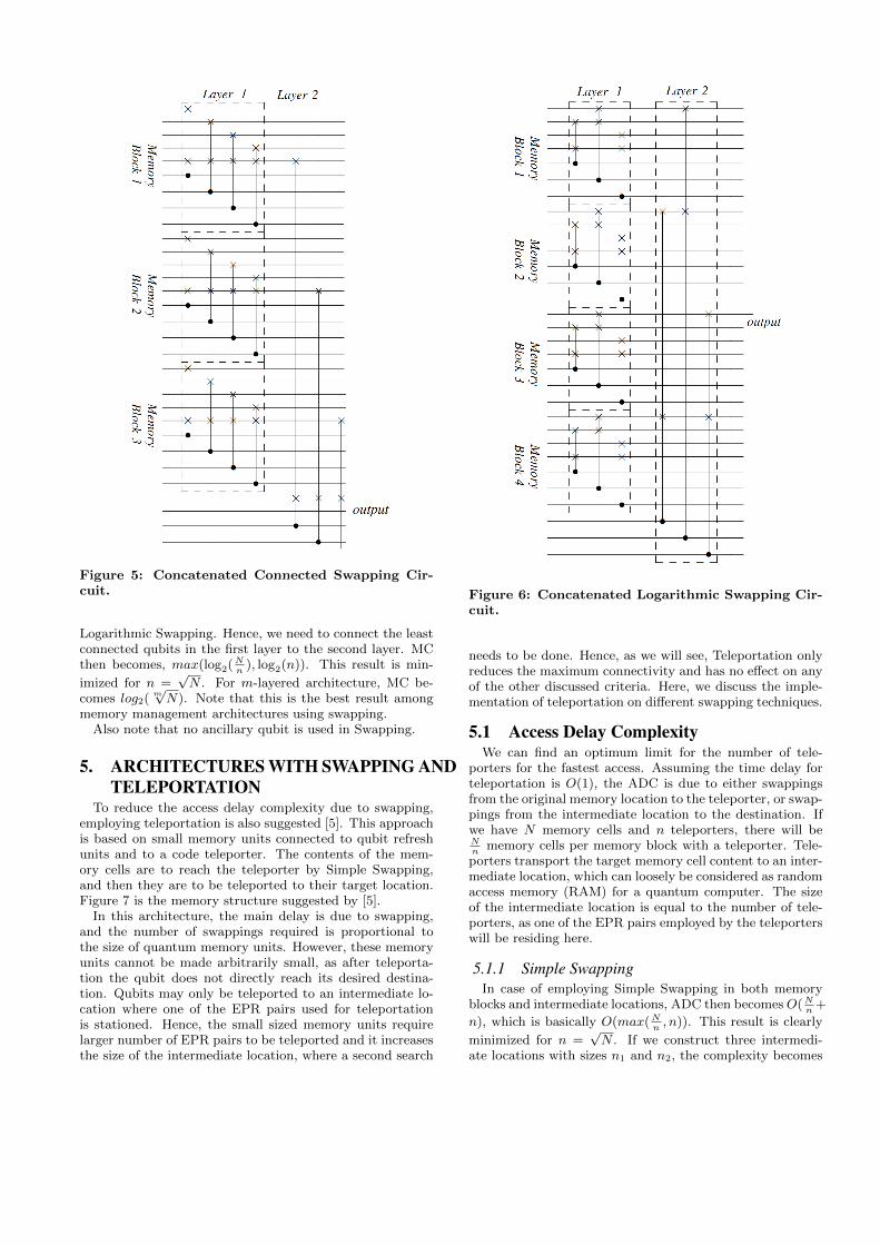
Figure 5: Concatenated Connected Swapping Cir-cuit.
Logarithmic Swapping. Hence, we need to connect the leastconnected qubits in the first layer to the second layer. MCthen becomes, max(log
2
(Nn
), log2
(n)). This result is min-
imized for n =pN . For m-layered architecture, MC be-
comes log2
( mpN). Note that this is the best result among
memory management architectures using swapping.Also note that no ancillary qubit is used in Swapping.
5. ARCHITECTURES WITH SWAPPING ANDTELEPORTATION
To reduce the access delay complexity due to swapping,employing teleportation is also suggested [5]. This approachis based on small memory units connected to qubit refreshunits and to a code teleporter. The contents of the mem-ory cells are to reach the teleporter by Simple Swapping,and then they are to be teleported to their target location.Figure 7 is the memory structure suggested by [5].
In this architecture, the main delay is due to swapping,and the number of swappings required is proportional tothe size of quantum memory units. However, these memoryunits cannot be made arbitrarily small, as after teleporta-tion the qubit does not directly reach its desired destina-tion. Qubits may only be teleported to an intermediate lo-cation where one of the EPR pairs used for teleportationis stationed. Hence, the small sized memory units requirelarger number of EPR pairs to be teleported and it increasesthe size of the intermediate location, where a second search
Figure 6: Concatenated Logarithmic Swapping Cir-cuit.
needs to be done. Hence, as we will see, Teleportation onlyreduces the maximum connectivity and has no e↵ect on anyof the other discussed criteria. Here, we discuss the imple-mentation of teleportation on di↵erent swapping techniques.
5.1 Access Delay ComplexityWe can find an optimum limit for the number of tele-
porters for the fastest access. Assuming the time delay forteleportation is O(1), the ADC is due to either swappingsfrom the original memory location to the teleporter, or swap-pings from the intermediate location to the destination. Ifwe have N memory cells and n teleporters, there will beN
n
memory cells per memory block with a teleporter. Tele-porters transport the target memory cell content to an inter-mediate location, which can loosely be considered as randomaccess memory (RAM) for a quantum computer. The sizeof the intermediate location is equal to the number of tele-porters, as one of the EPR pairs employed by the teleporterswill be residing here.
5.1.1 Simple SwappingIn case of employing Simple Swapping in both memory
blocks and intermediate locations, ADC then becomesO(Nn
+n), which is basically O(max(N
n
, n)). This result is clearly
minimized for n =pN . If we construct three intermedi-
ate locations with sizes n1
and n2
, the complexity becomes
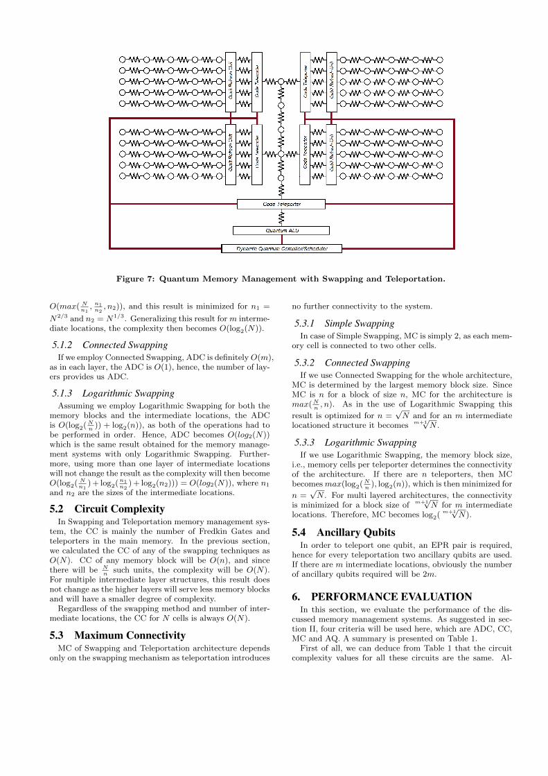
Figure 7: Quantum Memory Management with Swapping and Teleportation.
O(max( N
n1, n1n2
, n2
)), and this result is minimized for n1
=
N2/3 and n2
= N1/3. Generalizing this result for m interme-diate locations, the complexity then becomes O(log
2
(N)).
5.1.2 Connected SwappingIf we employ Connected Swapping, ADC is definitelyO(m),
as in each layer, the ADC is O(1), hence, the number of lay-ers provides us ADC.
5.1.3 Logarithmic SwappingAssuming we employ Logarithmic Swapping for both the
memory blocks and the intermediate locations, the ADCis O(log
2
(Nn
)) + log2
(n)), as both of the operations had tobe performed in order. Hence, ADC becomes O(log
2
(N))which is the same result obtained for the memory manage-ment systems with only Logarithmic Swapping. Further-more, using more than one layer of intermediate locationswill not change the result as the complexity will then becomeO(log
2
( N
n1)+ log
2
(n1n2
)+ log2
(n2
))) = O(log2
(N)), where n1
and n2
are the sizes of the intermediate locations.
5.2 Circuit ComplexityIn Swapping and Teleportation memory management sys-
tem, the CC is mainly the number of Fredkin Gates andteleporters in the main memory. In the previous section,we calculated the CC of any of the swapping techniques asO(N). CC of any memory block will be O(n), and sincethere will be N
n
such units, the complexity will be O(N).For multiple intermediate layer structures, this result doesnot change as the higher layers will serve less memory blocksand will have a smaller degree of complexity.
Regardless of the swapping method and number of inter-mediate locations, the CC for N cells is always O(N).
5.3 Maximum ConnectivityMC of Swapping and Teleportation architecture depends
only on the swapping mechanism as teleportation introduces
no further connectivity to the system.
5.3.1 Simple SwappingIn case of Simple Swapping, MC is simply 2, as each mem-
ory cell is connected to two other cells.
5.3.2 Connected SwappingIf we use Connected Swapping for the whole architecture,
MC is determined by the largest memory block size. SinceMC is n for a block of size n, MC for the architecture ismax(N
n
, n). As in the use of Logarithmic Swapping this
result is optimized for n =pN and for an m intermediate
locationed structure it becomes m+1pN .
5.3.3 Logarithmic SwappingIf we use Logarithmic Swapping, the memory block size,
i.e., memory cells per teleporter determines the connectivityof the architecture. If there are n teleporters, then MCbecomesmax(log
2
(Nn
), log2
(n)), which is then minimized for
n =pN . For multi layered architectures, the connectivity
is minimized for a block size of m+1pN for m intermediate
locations. Therefore, MC becomes log2
( m+1pN).
5.4 Ancillary QubitsIn order to teleport one qubit, an EPR pair is required,
hence for every teleportation two ancillary qubits are used.If there are m intermediate locations, obviously the numberof ancillary qubits required will be 2m.
6. PERFORMANCE EVALUATIONIn this section, we evaluate the performance of the dis-
cussed memory management systems. As suggested in sec-tion II, four criteria will be used here, which are ADC, CC,MC and AQ. A summary is presented on Table 1.
First of all, we can deduce from Table 1 that the circuitcomplexity values for all these circuits are the same. Al-
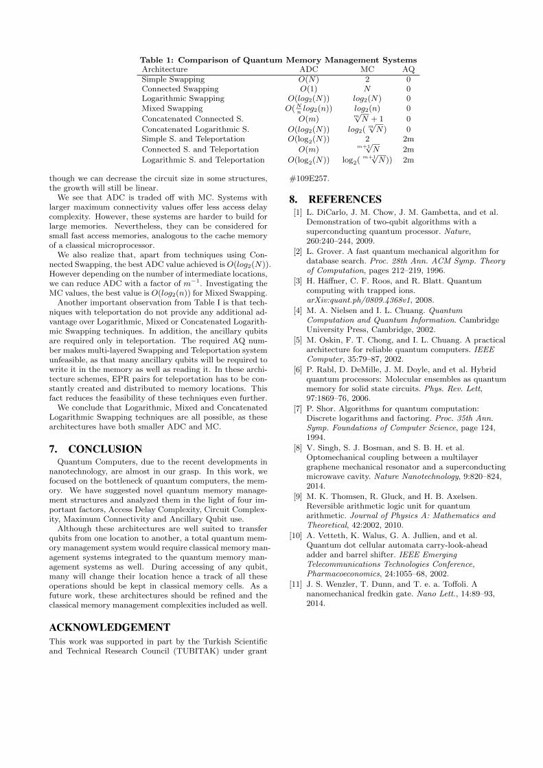
Table 1: Comparison of Quantum Memory Management SystemsArchitecture ADC MC AQSimple Swapping O(N) 2 0Connected Swapping O(1) N 0Logarithmic Swapping O(log
2
(N)) log2
(N) 0Mixed Swapping O(N
n
log2
(n)) log2
(n) 0Concatenated Connected S. O(m) m
pN + 1 0
Concatenated Logarithmic S. O(log2
(N)) log2
( mpN) 0
Simple S. and Teleportation O(log2
(N)) 2 2mConnected S. and Teleportation O(m) m+1
pN 2m
Logarithmic S. and Teleportation O(log2
(N)) log2
( m+1pN)) 2m
though we can decrease the circuit size in some structures,the growth will still be linear.
We see that ADC is traded o↵ with MC. Systems withlarger maximum connectivity values o↵er less access delaycomplexity. However, these systems are harder to build forlarge memories. Nevertheless, they can be considered forsmall fast access memories, analogous to the cache memoryof a classical microprocessor.
We also realize that, apart from techniques using Con-nected Swapping, the best ADC value achieved isO(log
2
(N)).However depending on the number of intermediate locations,we can reduce ADC with a factor of m�1. Investigating theMC values, the best value is O(log
2
(n)) for Mixed Swapping.Another important observation from Table I is that tech-
niques with teleportation do not provide any additional ad-vantage over Logarithmic, Mixed or Concatenated Logarith-mic Swapping techniques. In addition, the ancillary qubitsare required only in teleportation. The required AQ num-ber makes multi-layered Swapping and Teleportation systemunfeasible, as that many ancillary qubits will be required towrite it in the memory as well as reading it. In these archi-tecture schemes, EPR pairs for teleportation has to be con-stantly created and distributed to memory locations. Thisfact reduces the feasibility of these techniques even further.
We conclude that Logarithmic, Mixed and ConcatenatedLogarithmic Swapping techniques are all possible, as thesearchitectures have both smaller ADC and MC.
7. CONCLUSIONQuantum Computers, due to the recent developments in
nanotechnology, are almost in our grasp. In this work, wefocused on the bottleneck of quantum computers, the mem-ory. We have suggested novel quantum memory manage-ment structures and analyzed them in the light of four im-portant factors, Access Delay Complexity, Circuit Complex-ity, Maximum Connectivity and Ancillary Qubit use.
Although these architectures are well suited to transferqubits from one location to another, a total quantum mem-ory management system would require classical memory man-agement systems integrated to the quantum memory man-agement systems as well. During accessing of any qubit,many will change their location hence a track of all theseoperations should be kept in classical memory cells. As afuture work, these architectures should be refined and theclassical memory management complexities included as well.
ACKNOWLEDGEMENTThis work was supported in part by the Turkish Scientificand Technical Research Council (TUBITAK) under grant
#109E257.
8. REFERENCES[1] L. DiCarlo, J. M. Chow, J. M. Gambetta, and et al.
Demonstration of two-qubit algorithms with asuperconducting quantum processor. Nature,260:240–244, 2009.
[2] L. Grover. A fast quantum mechanical algorithm fordatabase search. Proc. 28th Ann. ACM Symp. Theory
of Computation, pages 212–219, 1996.[3] H. Ha↵ner, C. F. Roos, and R. Blatt. Quantum
computing with trapped ions.arXiv:quant.ph/0809.4368v1, 2008.
[4] M. A. Nielsen and I. L. Chuang. Quantum
Computation and Quantum Information. CambridgeUniversity Press, Cambridge, 2002.
[5] M. Oskin, F. T. Chong, and I. L. Chuang. A practicalarchitecture for reliable quantum computers. IEEEComputer, 35:79–87, 2002.
[6] P. Rabl, D. DeMille, J. M. Doyle, and et al. Hybridquantum processors: Molecular ensembles as quantummemory for solid state circuits. Phys. Rev. Lett,97:1869–76, 2006.
[7] P. Shor. Algorithms for quantum computation:Discrete logarithms and factoring. Proc. 35th Ann.
Symp. Foundations of Computer Science, page 124,1994.
[8] V. Singh, S. J. Bosman, and S. B. H. et al.Optomechanical coupling between a multilayergraphene mechanical resonator and a superconductingmicrowave cavity. Nature Nanotechnology, 9:820–824,2014.
[9] M. K. Thomsen, R. Gluck, and H. B. Axelsen.Reversible arithmetic logic unit for quantumarithmetic. Journal of Physics A: Mathematics and
Theoretical, 42:2002, 2010.[10] A. Vetteth, K. Walus, G. A. Jullien, and et al.
Quantum dot cellular automata carry-look-aheadadder and barrel shifter. IEEE Emerging
Telecommunications Technologies Conference,
Pharmacoeconomics, 24:1055–68, 2002.[11] J. S. Wenzler, T. Dunn, and T. e. a. To↵oli. A
nanomechanical fredkin gate. Nano Lett., 14:89–93,2014.