programmable logic controller analog input module analog input manuel.pdf · thank you for...
TRANSCRIPT
Right choice for ultimate yield LSIS strives to maximize customers' profit in gratitude of choosing us for your partner.
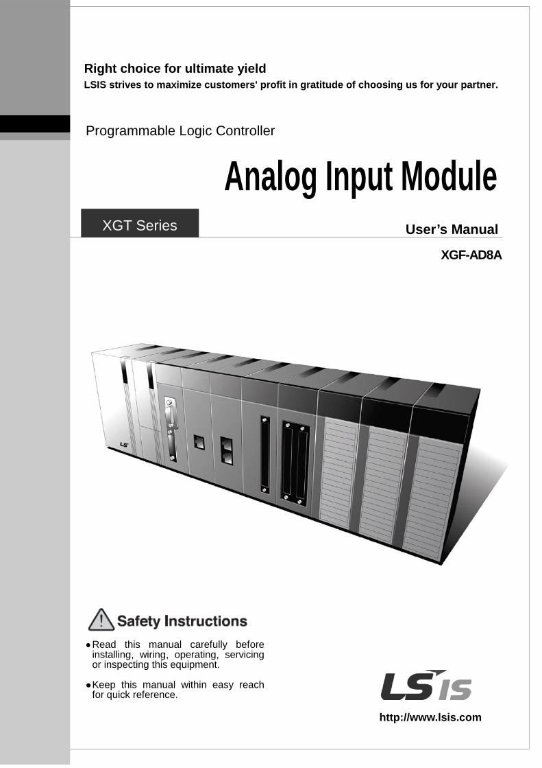
Programmable Logic Controller
Analog Input Module
User’s Manual
Read this manual carefully before installing, wiring, operating, servicing or inspecting this equipment.
Keep this manual within easy reach
for quick reference.
XGT Series
http://www.lsis.com
XGF-AD8A
Safety Instruction
Before using the product …
For your safety and effective operation, please read the safety instructions thoroughly before using the product.
Safety Instructions should always be observed in order to prevent accident or risk with the safe and
proper use the product.
Instructions are divided into “Warning” and “Caution”, and the meaning of the terms is as follows.
This symbol indicates the possibility of serious injury or death if some applicable
instruction is violated
This symbol indicates the possibility of severe or slight injury, and property
damages if some applicable instruction is violated
Moreover, even classified events under its caution category may develop into serious accidents relying on
situations. Therefore we strongly advise users to observe all precautions properly just like warnings.
The marks displayed on the product and in the user’s manual have the
following meanings.
Be careful! Danger may be expected.
Be careful! Electric shock may occur.
The user’s manual even after read shall be kept available and accessible to
any user of the product.
Warning
Caution
Safety Instruction
Safety Instructions for design process
Please install a protection circuit on the exterior of PLC so that the whole system may
operate safely regardless of failures from external power or PLC. Any abnormal output or
operation from PLC may cause serious problems to safety in whole system.
- Install protection units on the exterior of PLC like an interlock circuit that deals with opposite
operations such as emergency stop, protection circuit, and forward/reverse rotation or install an
interlock circuit that deals with high/low limit under its position controls.
- If any system error (watch-dog timer error, module installation error, etc.) is detected during
CPU operation in PLC, all output signals are designed to be turned off and stopped for safety.
However, there are cases when output signals remain active due to device failures in Relay and
TR which can’t be detected. Thus, you are recommended to install an addition circuit to monitor
the output status for those critical outputs which may cause significant problems.
Never overload more than rated current of output module nor allow to have a short circuit.
Over current for a long period time maycause a fire .
Never let the external power of the output circuit to be on earlier than PLC power, which may
cause accidents from abnormal output oroperation.
Please install interlock circuits in the sequence program for safe operations in the system
when exchange data with PLC or modify operation modes using a computer or other
external equipments Read specific instructions thoroughly when conducting control operations
with PLC.
Warning
Safety Instruction
Safety Instructions for design process
Safety Instructions on installation process
I/O signal or communication line shall be wired at least 100mm away from a high-voltage
cable or power line. Fail to follow this
Caution
Use PLC only in the environment specified in PLC manual or general standard of data
sheet. If not, electric shock, fire, abnormal operation of the product may be caused.
Before install or remove the module, be sure PLC power is off. If not, electric shock or damage
on the product may be caused.
Be sure that every module is securely attached after adding a module or an extension
connector. If the product is installed loosely or incorrectly, abnormal operation, error or dropping
may be caused. In addition, contact failures under poor cable installation will be causing
malfunctions as well.
Be sure that screws get tighten securely under vibrating environments. Fail to do so will put
the product under direct vibrations which will cause electric shock, fire and abnormal operation.
Do not come in contact with conducting parts in each module, which may cause electric
shock, malfunctions or abnormal operation.
Caution
Safety Instruction
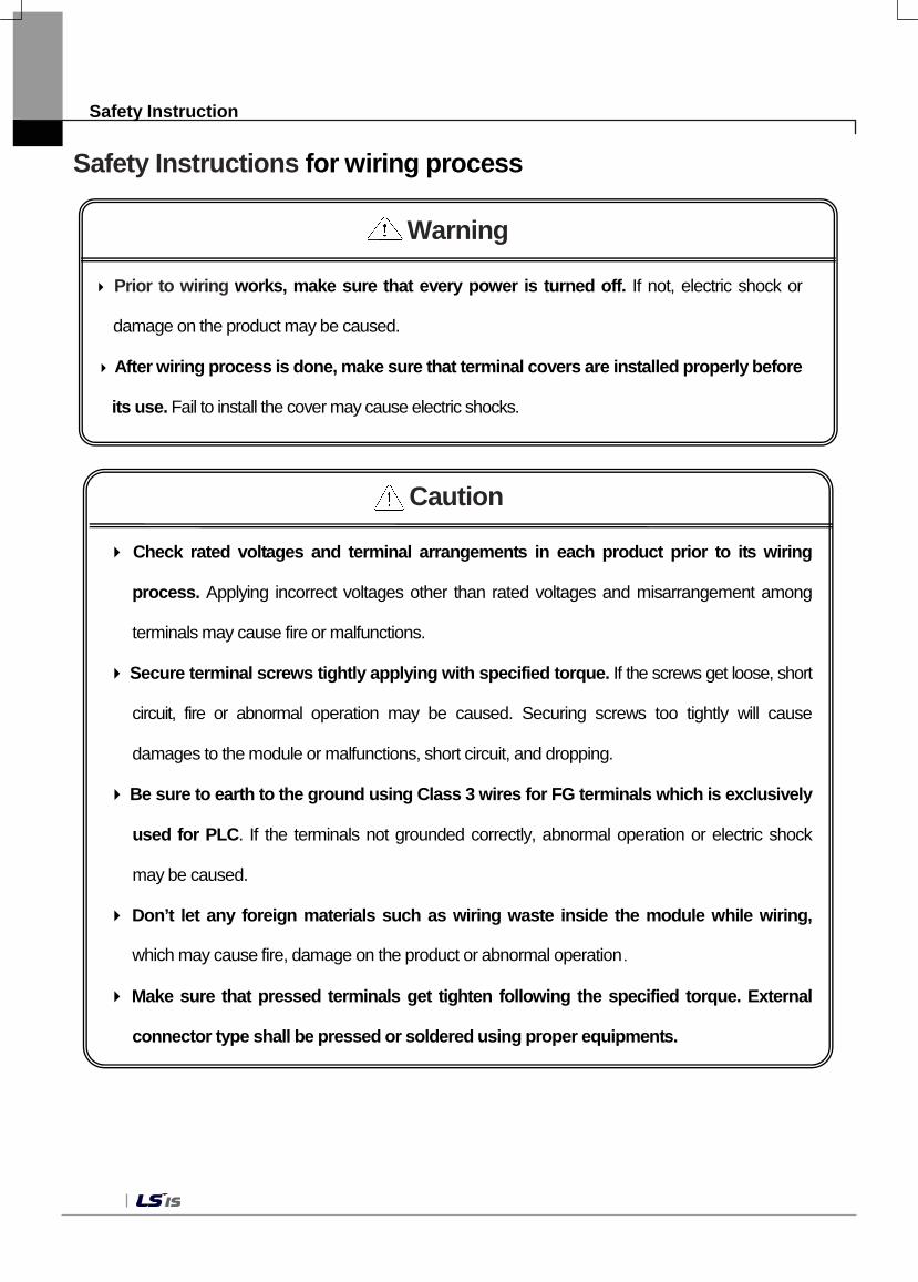
Safety Instructions for wiring process
Prior to wiring works, make sure that every power is turned off. If not, electric shock or
damage on the product may be caused.
After wiring process is done, make sure that terminal covers are installed properly before
its use. Fail to install the cover may cause electric shocks.
Warning
Check rated voltages and terminal arrangements in each product prior to its wiring
process. Applying incorrect voltages other than rated voltages and misarrangement among
terminals may cause fire or malfunctions.
Secure terminal screws tightly applying with specified torque. If the screws get loose, short
circuit, fire or abnormal operation may be caused. Securing screws too tightly will cause
damages to the module or malfunctions, short circuit, and dropping.
Be sure to earth to the ground using Class 3 wires for FG terminals which is exclusively
used for PLC. If the terminals not grounded correctly, abnormal operation or electric shock
may be caused.
Don’t let any foreign materials such as wiring waste inside the module while wiring,
which may cause fire, damage on the product or abnormal operation.
Make sure that pressed terminals get tighten following the specified torque. External
connector type shall be pressed or soldered using proper equipments.
Caution
Safety Instruction
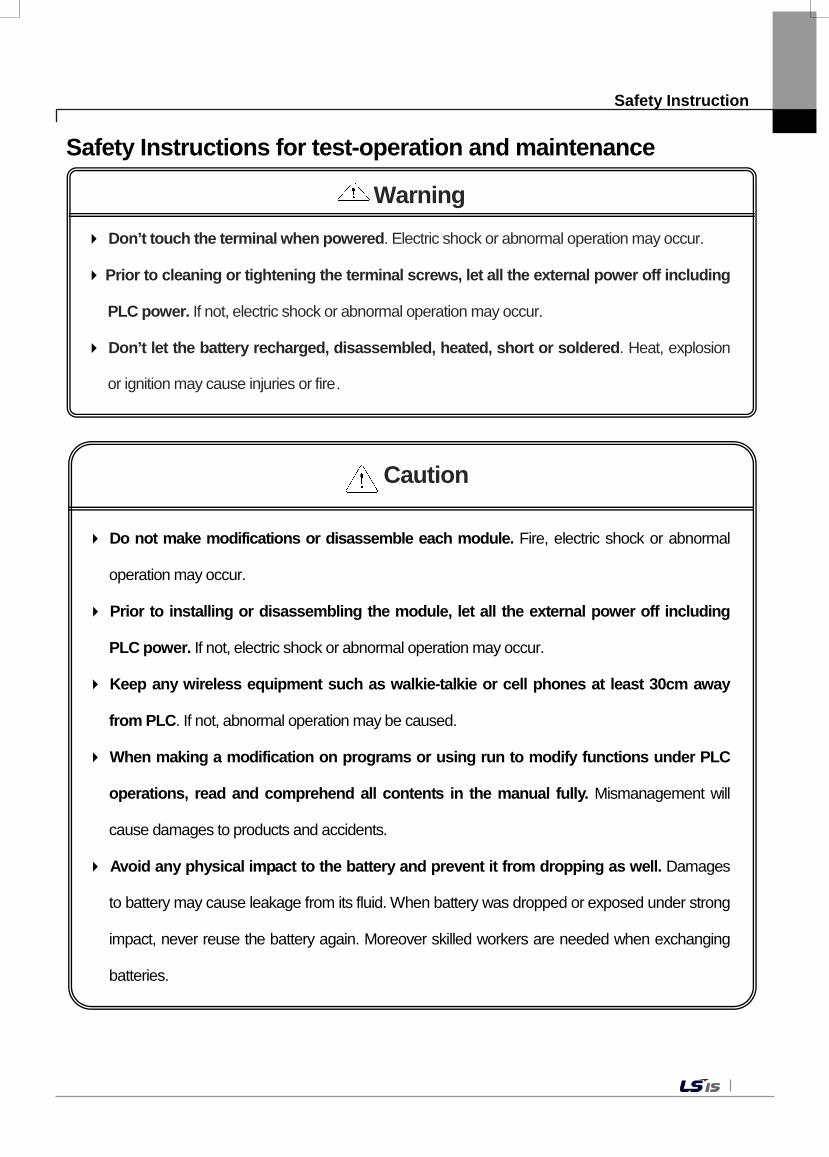
Safety Instructions for test-operation and maintenance
Don’t touch the terminal when powered. Electric shock or abnormal operation may occur.
Prior to cleaning or tightening the terminal screws, let all the external power off including
PLC power. If not, electric shock or abnormal operation may occur.
Don’t let the battery recharged, disassembled, heated, short or soldered. Heat, explosion
or ignition may cause injuries or fire.
Warning
Do not make modifications or disassemble each module. Fire, electric shock or abnormal
operation may occur.
Prior to installing or disassembling the module, let all the external power off including
PLC power. If not, electric shock or abnormal operation may occur.
Keep any wireless equipment such as walkie-talkie or cell phones at least 30cm away
from PLC. If not, abnormal operation may be caused.
When making a modification on programs or using run to modify functions under PLC
operations, read and comprehend all contents in the manual fully. Mismanagement will
cause damages to products and accidents.
Avoid any physical impact to the battery and prevent it from dropping as well. Damages
to battery may cause leakage from its fluid. When battery was dropped or exposed under strong
impact, never reuse the battery again. Moreover skilled workers are needed when exchanging
batteries.
Caution
Safety Instruction
Safety Instructions for waste disposal
Product or battery waste shall be processed as industrial waste. The waste may discharge
toxic materials or explode itself.
Caution
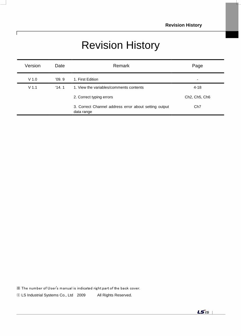
Revision History
Revision History
Version Date Remark Page
V 1.0 ’09. 9 1. First Edition -
V 1.1 ‘14. 1 1. View the variables/comments contents 4-18
2. Correct typing errors Ch2, Ch5, Ch6
3. Correct Channel address error about setting output data range
Ch7
※ The number of User’s manual is indicated right part of the back cover.
LS Industrial Systems Co., Ltd 2009 All Rights Reserved.
About User’s Manual
1
Thank you for purchasing PLC of LS Industrial System Co.,Ltd. Before use, make sure to carefully read and understand the User’s Manual about the functions, performances, installation and programming of the product you purchased in order for correct use and importantly, let the end user and maintenance administrator to be provided with the User’s Manual. The User’s Manual describes the product. If necessary, you may refer to the following description and order accordingly. In addition, you may connect our website (http://www.lsis.com/) and download the information as a PDF file.
Relevant User’s Manuals
Title Description
XG5000 User’s Manual (for XGK, XGB)
XG5000 software user manual describing online function such as programming, print, monitoring, debugging by using XGK, XGB CPU
XG5000 User’s Manual (for XGI, XGR)
XG5000 software user manual describing online function such as programming, print, monitoring, debugging by using XGI, XGR CPU
XGK/XGB Instructions & Programming User’s Manual
User’s manual for programming to explain how to use instructions that are used PLC system with XGK, XGB CPU.
XGI/XGR/XEC Instructions & Programming User’s Manual
User’s manual for programming to explain how to use instructions that are used PLC system with XGI, XGR,XEC CPU.
XGK CPU User’s Manual (XGK-CPUA/CPUE/CPUH/CPUS/CPUU)
XGK-CPUA/CPUE/CPUH/CPUS/CPUU user manual describing about XGK CPU module, power module, base, IO module, specification of extension cable and system configuration, EMC standard
XGI CPU User’s Manual (XGI-CPUU/CPUH/CPUS)
XGI-CPUU/CPUH/CPUS user manual describing about XGI CPU module, power module, base, IO module, specification of extension cable and system configuration, EMC standard
XGR redundant series User’s Manual
XGR- CPUH/F, CPUH/T user manual describing about XGR CPU module, power module, extension drive, base, IO module, specification of extension cable and system configuration, EMC standard
Current XGF-AD16A manual is written based on the following version.
Related OS version list
Product name OS version
XGK-CPUH, CPUS, CPUA, CPUE, CPUU V2.1
XGI-CPUU, CPUH, CPUS V2.2
XGR-CPUH/F, CPUH/T V1.3
XG5000(XG-PD) V2.41
Contents
1
Contents
Chapter 1 Overview ……………………………………………………………………………………… 1-1 ~ 1-4
1.1 Characteristics …………………………………………………………………………………………………………………… 1-1
1.2 Glossary …………………………………………………………………………………………………………………………… 1-2
1.2.1 Analog Quantity - A ………………………………………………………………………………………………………… 1-2
1.2.2 Digital Quantity - D ………………………………………………………………………………………………………… 1-2
1.2.3 The Characteristics of Analog-Digital Conversion ……………………………………………………………………… 1-3
1.3 New Functions …………………………………………………………………………………………………………………… 1-4
Chapter 2 Specifications ……………………………………………………………………………… 2-1 ~ 2-20
2.1 General Specifications …………………………………………………………………………………………………………… 2-1
2.2 Performance Specifications ……………………………………………………………………………………………………… 2-2
2.3 Description of the Parts ………………………………………………………………………………………………………… 2-4
2.4 Characteristics of Input/Output Conversion …………………………………………………………………………………… 2-5
2.4.1 Input/Output Characteristics of XGF-AD8A ……………………………………………………………………………… 2-6
2.4.2 Precision ………………………………………………………….………………………………………………………… 2-13
2.5 Functions of the Analog Input Module ……………………………………………………………………………………… 2-14
2.5.1 Sampling Processing ……………………………………………………………………………………………………… 2-14
2.5.2 Average Processing ……………………………………………………………………………………………………… 2-15
2.5.3 Detection of Input Disconnection ……………………………………………………………………………………… 2-17
2.5.4 Hold last value (Dedicated for current input) …………………………………………………………………………… 2-19
2.5.5 Alarm function ……………………………………………………………………………………………………………… 2-19
Chapter 3 Installation and Wiring ……………………………………………………………………… 3-1 ~ 3-4
3.1 Installation ………………………………………………………………………………………………………………………… 3-1
3.1.1 Installation Environment ………………………………………………………………………..………………………… 3-1
3.1.2 Precautions in Handling …………………………………………………………………………………………………… 3-1
3.2 Wiring ……………………………………………………………………………………………………………………………… 3-2
3.2.1 Precautions in Wiring ……………………………………………………………………………………………………… 3-2
3.2.2 An Example of Wiring ………………………………………………………………………………………………… 3-2
Contents
2
Chapter 4 Operating Setting …………………………………………………………………………… 4-1 ~ 4-17
4.1 The Operating Setting Flowchart ……………………………………………………………………………………………… 4-1
4.2 Operating Parameter Setting …………………………………………………………………………………………………… 4-2
4.2.1 Setting Items ………………………………………………………..……………………………………………………… 4-2
4.2.2 How to Use [I/O Parameter] ………………………………………………………………………………………………… 4-2
4.3 Functions of the Special Module Monitor ……………………………………………………………………………………… 4-6
4.4 Precautions ………………………………………………………………………………………………………………………… 4-7
4.5 How to Use the Special Module Monitor ……………………………………………………………………………………… 4-8
4.5.1 Starting [Special module monitoring] …………………………………………………………………………………… 4-8
4.5.2 How to Use [Special module monitoring] ……………………………………………….……………………………… 4-8
4.6 U Automatic Registration of U Device ………………………………………………………………………………………… 4-12
4.6.1 Automatic Registration of U Device …………………………………………………………………………………… 4-12
4.6.2 Saving Variables …………………………………………………………………………………………………………… 4-14
4.6.3 Viewing Variables in the Program ……………………………………………………………………………………… 4-15
Chapter 5 Configuration and Functions of the Internal Memory (XGK)…..……………………… 5-1 ~ 5-11
5.1 The Configuration of the Internal Memory …………………………………………………………………………………… 5-1
5.1.1 Input and Output Areas of A/D Conversion Data ……………………………………………………………………… 5-1
5.1.2 Operating Parameter Setting Range ……………………………………………………………………………………… 5-3
5.2 A/D Conversion Data Input/Output Ranges …………………………………………………………………………………… 5-4
5.2.1 Module READY/ERROR Flag ……………………………………………………………………………………………… 5-4
5.2.2 Operating channel flag ……………………………………………………………………………………………………… 5-4
5.2.3 Digital output value ………………………………………………………………………………………………………… 5-5
5.2.4 Disconnection detection flag ……………………………………………………………………………………………… 5-5
5.2.5 Error clear request flag …………………………………………………………………………………………………… 5-5
5.3 Operating Parameter Setting Ranges ………………………………………………………………………………………… 5-6
5.3.1 Designation of the channel to use ………………………………………………………………………………………… 5-6
5.3.2 Output Voltage/Current Ranges …………………………………………………….…………………………………… 5-7
5.3.3 Output Data Ranges ……………………………………………………………………………………………………… 5-7
5.3.4 Average Processing ………………………………………………………………………………………………………… 5-8
5.3.5 Average Value ……………………………………………………………………………………………………………… 5-8
5.3.6 Error Code ………………………………………………………………………………………………………………… 5-10
5.3.7 Hold last value ……………………………………………………………………………………………………… 5-11
Contents
3
Chapter 6 Programming (XGK) ………………………………………………………………………… 6-1 ~ 6-7
6.1 The Basic Program ……………………………………………………………………………………………………………… 6-1
6.1.1 An Example of a Program That Uses [I/O Parameter] ………………………………………………………………… 6-1
6.1.2 An Example of a Program That Uses the PUT/GET Command ……………………………………………………… 6-2
6.2 Application Program (XGK) …………………………………………………………….……………………………………… 6-3
6.2.1 The Program Distinguishing A/D Conversion Values ………………………………………………………………… 6-3
6.2.2 The Program That Outputs the Error Code of the Analog Input Module through BCD Display ………………… 6-6
Chapter 7 Configuration and Functions of Global Variables (for XGI/XGR)…………………… 7-1 ~ 7-17
7.1 Global Variables (Data Areas)…………………………………………………………………………………………………… 7-1
7.1.1 Configuration of A/D Conversion Data Input and Output Area ……………………………………… 7-1
7.1.2 How to Use Global Variables ……………………………………………………………………………………………… 7-2
7.2 PUT/GET Function Block Area (Parameter Area)…………………………………………………………………………… 7-10
7.2.1 PUT/GET Function Block Area (Parameter Area) …………………………………………………………………… 7-10
7.2.2 PUT/GET Commands ……………………………………………………………………………………………………… 7-11
7.2.3 Examples of Use of PUT/GET Commands ………………………………………….………………………………… 7-13
Chapter 8 Programming (XGI, XGR) ………………………………………………………………… 8-1 ~ 8-9
8.1 The Basic Program (XGI/XGR) ………………………………………………………………………………………………… 8-1
8.1.1 An Example of a Program That Uses [I/O Parameter] ………………………………………………………………… 8-1
8.1.2 An Example of a Program That Uses the PUT/GET Command ……………………………………………………… 8-3
8.2 Application Program (XGI/XGR) ……………………………………..………………………………………………………… 8-5
8.2.1 The Program Distinguishing A/D Conversion Values ………………………………………………………………… 8-5
8.2.2 The Program That Outputs the Error Code of the Analog Input Module through BCD Display ………………… 8-8
Chapter 9 Failure Check ………………………………………………………………………………… 9-1 ~ 9-5
9.1 Error Code ………………………………………………………………………………………………………………………… 9-1
9.2 Failure Check ……………………………………………………………………………………………………………………… 9-2
9.2.1 RUN LED Flashes …………………………………………………………………………………………………………… 9-2
9.2.2 RUN LED is Off ………………………………………………………………………………………………………… 9-3
9.2.3 CPU Module Cannot Read A/D Conversion Values …………………………………………………………………… 9-3
9.2.4 The Analog Input Value Inconsistent with Digital Output Value. …………………………………………………… 9-4
Contents
4
9.2.5 Hardware Failure of the Analog Input Module …………………………………………………………………………… 9-4
9.2.6 Check of Analog Input Module Status by XG5000 System Monitor ………………………………………………… 9-4
Appendix1 Glossary…….………………………………………………………………………..…… A1-1~A1-2
Appendix 1 Glossary ………………………………………………………………………………………………… A1-1
Appendix2 Dimension ……………………………………………………………………………………… A2-1
Appendix2 Dimension …………………………………………………………………………………………………………… A2-1
Chapter 1 Overview
1-1
Chapter 1 Overview This manual describes the specifications, handling, and programming of the XGF-AD8A type analog/digital conversion
module, which is used in combination with the CPU module of the XGT PLC series. XGF-AD8A is hereafter referred to as the analog input module. The analog input module is for converting the analog signals (voltage or current input) from a PLC external device into digital values of the signed 14 bit binary data.
1.1 Characteristics
1) Hybrid input processing 8 channel current/voltage input can be processed in a single module.
2) High speed conversion Conversion can be conducted at a high speed of 250/channel.
3) High precision The conversion precision is ±0.2%(surrounding temperature 25 ± 5 ).
4) High resolution of 1/16000 The resolution of the digital values can be set at 1/16000.
5) Operating parameter setting and monitoring by GUI(Graphical User Interface) The operating setting, which was conducted by commands, can be manipulated by using [I/O parameter
setting] with improved user interface, which increased the user’s convenience. You can reduce the sequence program by using I/O parameter setting. Furthermore, you can easily monitor the A/D converted values using [Special module monitor] function.
6) A variety of digital output data formats 4 types of digital output data format are supported. The output type of the digital data can be defined as follows. Unsigned value: 0 ~ 16000 Signed value: -8000 ~ 8000 Precise value: see Chapter 2.2. Percentile value: 0 ~ 10000
7) Short circuit detection A short circuit of the input circuit can be detected when the analog input sign range of 4 ~ 20 mA, 1 ~ 5 V is used.

Chapter 1 Overview
1-2
[Fig.1.1] Analog quantity [Fig.1.2] An example of the transducer
1.2.1 Analog Quantity - A Analog quantity refers to when a physical value is continuous. As analog values are unbroken, there is always a
median value. Physical properties in general such as voltage, current, velocity, pressure and flow fall into the analog quantity. For example, the temperature is seamless over time as shown in Fig. 1.1 Because the temperature cannot be input directly into the Analog input module, it needs to be relayed by a transducer that converts input signals of analog properties into electrical signals.
1.2.2 Digital Quantity - D
The data consisting of integers or the physical properties in figures are referred to as digital properties (Fig. 1.3). The digital properties are the electronic method of creating, storing and processing the data in only 0 and 1. The data transmitted or stored by digital technology is expressed in a string of 0 and 1. For example, the on and off signals can be expressed in 0 and 1 digital values, and the BCD or binary values are also digital values.
Analog values cannot be directly input in the PLC CPU for an operation. That is why the analog values are converted in digital values when they are input in the PLC CPU as shown in Fig. 1.4. This is carried out by the Analog input module. In addition, for the analog values to be output to the outside, the PLC CPU digital values should be converted into analog values. This function is conducted by the D/A conversion module.
1.2 Glossary
CPU (digital operation)
A/D convers
ion
D/A convers
ion
Analog input 0~10V, 1~5V
Or 4~20
Analog output 0~10V, -10~10V
or 4~20
[Fig. 1.4] Process at PLC
time
Te
Time
Te
temp
0~1000
Transducer Voltage: input-
10~+10V A/D
i d l
Chapter 1 Overview
1-3
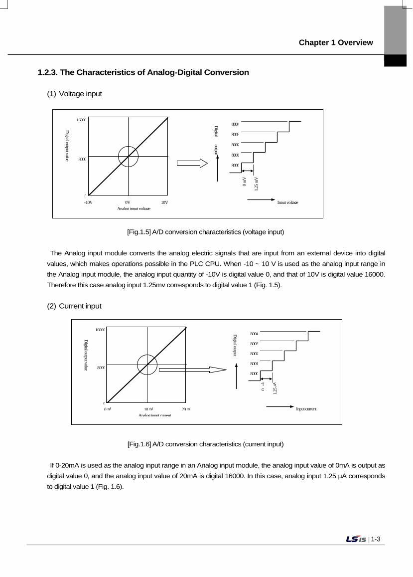
1.2.3. The Characteristics of Analog-Digital Conversion
(1) Voltage input
[Fig.1.5] A/D conversion characteristics (voltage input)
The Analog input module converts the analog electric signals that are input from an external device into digital values, which makes operations possible in the PLC CPU. When -10 ~ 10 V is used as the analog input range in the Analog input module, the analog input quantity of -10V is digital value 0, and that of 10V is digital value 16000. Therefore this case analog input 1.25mv corresponds to digital value 1 (Fig. 1.5). (2) Current input
[Fig.1.6] A/D conversion characteristics (current input)
If 0-20mA is used as the analog input range in an Analog input module, the analog input value of 0mA is output as digital value 0, and the analog input value of 20mA is digital 16000. In this case, analog input 1.25 µA corresponds to digital value 1 (Fig. 1.6).
8004
8002
8001
8000
8003
0
1.25
Input current
Digital output value
16000
8000
0 0 10 20
Analog input current
Digital output
8004
8002
8001
8000
8003
0 mV
1.25 m
V
Input voltage
Digital output value
16000
8000
0 -10V 0V 10V
Analog input voltage
Digital
output
Chapter 1 Overview
1-4
1.3. New Functions
The new functions of Analog input module are as follows.
Item Description
Module
OS
version
CPU OS
version Ref.
Hold last
value
When input signal exceeds effective range, holds last
effective input value. V1.02
Not
related 2.5
Alarm
function
When input signal exceeds effective range, relevant
alarm flag turns on. V1.02
XGK
V3.2
XGI V3.1
XGR
V1.7
2.5
Chapter 2 Specifications
2-1
Chapter 2 Specifications
2.1 General Specifications
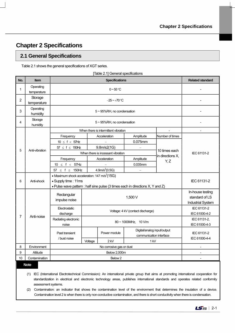
Table 2.1 shows the general specifications of XGT series.
[Table 2.1] General specifications
No. Item Specifications Related standard
1 Operating
temperature 0 ~ 55 C -
2 Storage
temperature 25 ~ 70 C -
3 Operating humidity
5 ~ 95%RH, no condensation -
4 Storage
humidity 5 ~ 95%RH, no condensation -
5 Anti-vibration
When there is intermittent vibration - -
Frequency Acceleration Amplitude Number of times
IEC 61131-2
10 f 57Hz 0.075mm
10 times each
in directions X, Y, Z
57 f 150Hz 9.8m/s2(1G)
When there is incessant vibration
Frequency Acceleration Amplitude
10 f 57Hz 0.035mm
57 f 150Hz 4.9m/s2(0.5G)
6 Anti-shock
Maximum shock acceleration: 147 m/s2(15G) Supply time : 11ms
Pulse wave pattern : half sine pulse (3 times each in directions X, Y and Z)
IEC 61131-2
7 Anti-noise
Rectangular impulse noise
1,500 V
In-house testing
standard of LS
Industrial System
Electrostatic
discharge Voltage: 4 kV (contact discharge)
IEC 61131-2
IEC 61000-4-2
Radiating electronic
noise 80 ~ 1000MHz, 10 V/m
IEC 61131-2,
IEC 61000-4-3
Past transient
/ bust noise
Power moduleDigital/analog input/output
communication interface IEC 61131-2
IEC 61000-4-4 Voltage 2 kV 1 kV
8 Environment No corrosive gas or dust -
9 Altitude Below 2,000m -
10 Contamination Below 2 -
(1) IEC (International Electrotechnical Commission): An international private group that aims at promoting international cooperation for
standardization in electrical and electronic technology areas, publishes international standards and operates related conformity
assessment systems.
(2) Contamination: an indicator that shows the contamination level of the environment that determines the insulation of a device.
Contamination level 2 is when there is only non-conductive contamination, and there is short conductivity when there is condensation.
Note
Chapter 2 Specifications
2-2
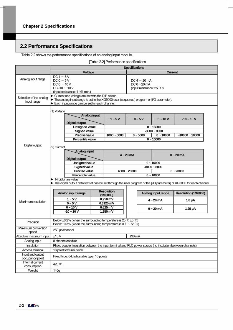
2.2 Performance Specifications Table 2.2 shows the performance specifications of an analog input module.
[Table 2.2] Performance specifications
Specifications Voltage Current
Analog input range
DC 1 ∼ 5 VDC 0 ∼ 5 V DC 0 ∼ 10 V DC -10 ∼ 10 V (input resistance: 1 min.)
DC 4 ∼ 20 mA DC 0 ~ 20 mA (input resistance: 250 Ω)
Selection of the analog input range
Current and voltage are set with the DIP switch. The analog input range is set in the XG5000 user (sequence) program or [i/O parameter]. Each input range can be set for each channel.
Digital output
(1) Voltage
Analog input
Digital output 1 ~ 5 V 0 ~ 5 V 0 ~ 10 V -10 ~ 10 V
Unsigned value 0 ~ 16000Signed value -8000 ~ 8000Precise value 1000 ~ 5000 0 ~ 5000 0 ~ 10000 -10000 ~ 10000
Percentile value 0 ~ 10000 (2) Current
Analog input
Digital output 4 ~ 20 mA 0 ~ 20 mA
Unsigned value 0 ~ 16000Signed value -8000 ~ 8000Precise value 4000 ~ 20000 0 ~ 20000
Percentile value 0 ~ 10000 14 bit binary value The digital output data format can be set through the user program or the [i/O parameter] of XG5000 for each channel.
Maximum resolution
Analog input range Resolution (1/16000)
1 ~ 5 V 0.250 mV0 ~ 5 V 0.3125 mV0 ~ 10 V 0.625 mV
-10 ~ 10 V 1.250 mV
Analog input range Resolution (1/16000)
4 ~ 20 mA 1.0 µA
0 ~ 20 mA 1.25 µA
Precision Below ±0.2% (when the surrounding temperature is 25 ±5 )Below ±0.3% (when the surrounding temperature is 0 ~ 55 )
Maximum conversion speed 250 μs/channel
Absolute maximum input ±15 V ±30 mA Analog input 8 channel/module
Insulation Photo coupler insulation between the input terminal and PLC power source (no insulation between channels) Access terminal 18 point terminal block Input and output occupancy point
Fixed type: 64, adjustable type: 16 points
Internal current consumption
420
Weight 140g
Chapter 2 Specifications
2-3
Note (1) The analog input module has the offset and gain values set for each analog input range when it is manufactured. The user cannot change the
values.
(2) The voltage/current selection switch is set at current when shipped at the factory.
(3) Offset value: the analog input value of which the digital output value is 0 when the digital output type is set as an unsigned value
(4) Gain value: the analog input value of which the digital output value is 16000 when the digital output type is set as an unsigned value
(5) The XGR system can be used at the extended base, not the basic base.
Chapter 2 Specifications
2-4
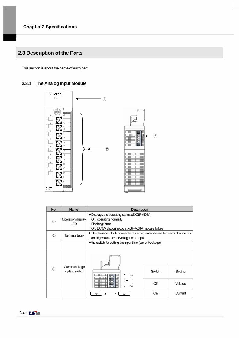
2.3 Description of the Parts
This section is about the name of each part.
2.3.1 The Analog Input Module
No. Name Description
① Operation display
LED
Displays the operating status of XGF-AD8A On: operating normally Flashing: error Off: DC 5V disconnection, XGF-AD8A module failure
② Terminal block The terminal block connected to an external device for each channel for
analog value current/voltage to be input
③ Current/voltage setting switch
the switch for setting the input time (current/voltage)
Switch Setting
Off Voltage
On Current
①
②
③
Ch0
Ch7
.
.
Off On
Chapter 2 Specifications
2-5
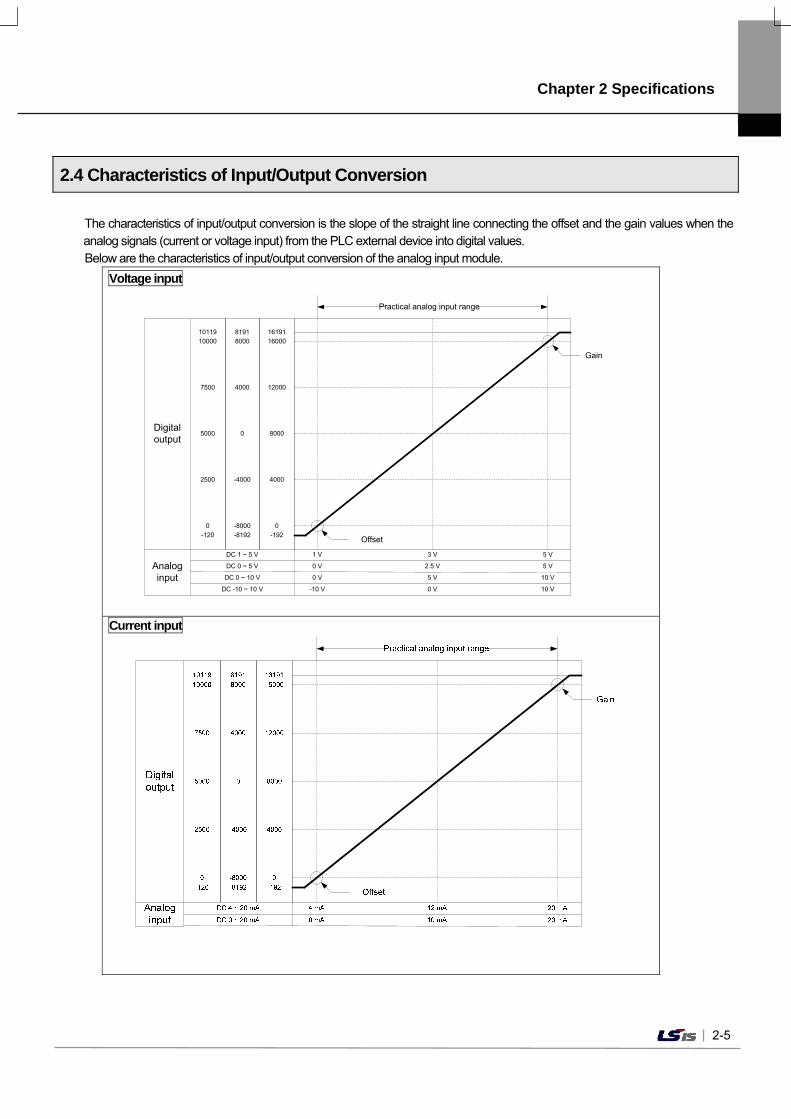
2.4 Characteristics of Input/Output Conversion
The characteristics of input/output conversion is the slope of the straight line connecting the offset and the gain values when the analog signals (current or voltage input) from the PLC external device into digital values. Below are the characteristics of input/output conversion of the analog input module.
Voltage input
Digital output
0
4000
8000
12000
16000
16191
-192
-8000
-4000
0
4000
8000
8191
-8192
0
2500
5000
7500
10000
10119
-120
DC 1 ~ 5 V
DC 0 ~ 5 V
DC 0 ~ 10 V
DC -10 ~ 10 V
1 V 5 V3 V
0 V 2.5 V 5 V
0 V 5 V 10 V
-10 V 0 V 10 V
Analog input
Practical analog input range
Offset
Gain
Current input
Chapter 2 Specifications
2-6
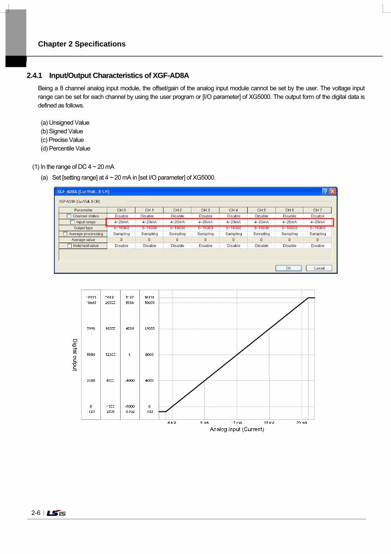
2.4.1 Input/Output Characteristics of XGF-AD8A Being a 8 channel analog input module, the offset/gain of the analog input module cannot be set by the user. The voltage input range can be set for each channel by using the user program or [I/O parameter] of XG5000. The output form of the digital data is defined as follows.
(a) Unsigned Value (b) Signed Value (c) Precise Value (d) Percentile Value
(1) In the range of DC 4 ~ 20 mA
(a) Set [setting range] at 4 ~ 20 mA in [set I/O parameter] of XG5000.
Chapter 2 Specifications
2-7
(b) The digital output values for the current input characteristics are as follows.
(Resolution (for 1/16000): 1 μA)
Digital output range
Analog input current (mA)
3.808 4 8 12 16 20 20.191
Unsigned value
(-192 ~ 16191) -192 0 4000 8000 12000 16000 16191
Signed value
(-8192 ~ 8191) -8192 -8000 -4000 0 4000 8000 8191
Precise value
(3808 ~ 20191) 3808 4000 8000 12000 16000 20000 20191
Percentile value
(-120 ~ 10119) -120 0 2500 5000 7500 10000 10119
(2) In the range of DC 0 ~ 20 mA
(a) Set [setting range] at 0 ~ 20 mA in [set I/O parameter] of XG5000.
Chapter 2 Specifications
2-8
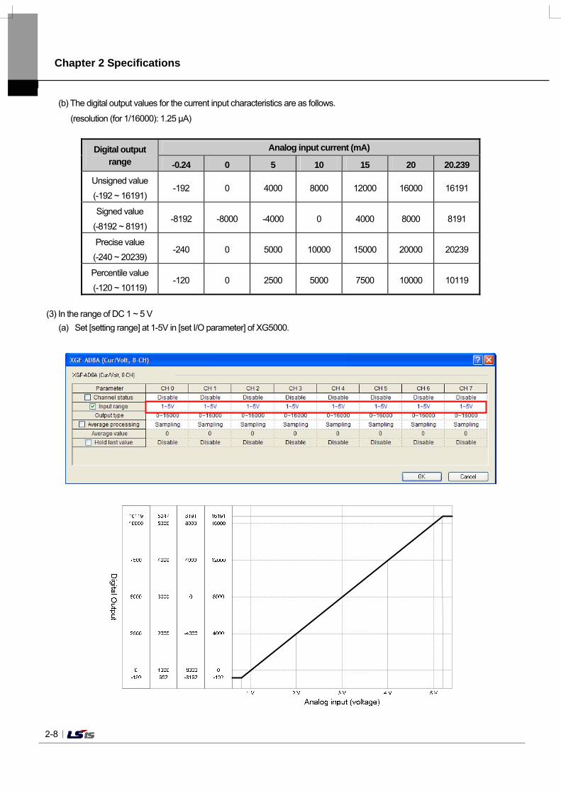
(b) The digital output values for the current input characteristics are as follows.
(resolution (for 1/16000): 1.25 μA)
Digital output range
Analog input current (mA)
-0.24 0 5 10 15 20 20.239
Unsigned value
(-192 ~ 16191) -192 0 4000 8000 12000 16000 16191
Signed value
(-8192 ~ 8191) -8192 -8000 -4000 0 4000 8000 8191
Precise value
(-240 ~ 20239) -240 0 5000 10000 15000 20000 20239
Percentile value
(-120 ~ 10119) -120 0 2500 5000 7500 10000 10119
(3) In the range of DC 1 ~ 5 V
(a) Set [setting range] at 1-5V in [set I/O parameter] of XG5000.
Chapter 2 Specifications
2-9
(b) The digital output values for the voltage input characteristics are as follows.
(resolution (for 1/16000): 0.25 mV)
Digital output range
Analog input voltage (V)
0.952 1 2 3 4 5 5.047
Unsigned value
(-192 ~ 16191) -192 0 4000 8000 12000 16000 16191
Signed value
(-8192 ~ 8191) -8192 -8000 -4000 0 4000 8000 8191
Precise value
(952 ~ 5047) 952 1000 2000 3000 4000 5000 5047
Percentile value
(-120 ~ 10119) -120 0 2500 5000 7500 10000 10119
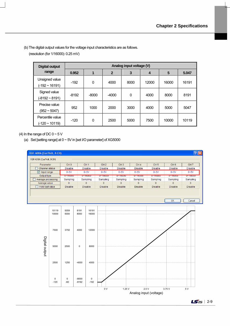
(4) In the range of DC 0 ~ 5 V
(a) Set [setting range] at 0 ~ 5V in [set I/O parameter] of XG5000
Digital output
0
4000
8000
12000
16000
16191
-192
-8000
-4000
0
4000
8000
8191
-8192
0
2500
5000
7500
10000
10119
-120
0 V 5 V2.5 V
5059
5000
3750
2500
1250
0
-60
3.75 V1.25 V
Analog input (voltage)
Chapter 2 Specifications
2-10
(b) The digital output values for the voltage input characteristics are as follows.
(resolution (for 1/16000): 0.3125 mV)
Digital output range
Analog input voltage (V)
-0.06 0 1.25 2.5 3.75 5 5.05
Unsigned value
(-192 ~ 16191) -192 0 4000 8000 12000 16000 16191
Signed value
(-8192 ~ 8191) -8192 -8000 -4000 0 4000 8000 8191
Precise value
(-60 ~ 5060) -60 0 1250 2500 3750 5000 5059
Percentile value
(-120 ~ 10119) -120 0 2500 5000 7500 10000 10119
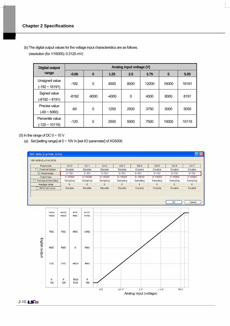
(5) In the range of DC 0 ~ 10 V
(a) Set [setting range] at 0 ~ 10V in [set I/O parameter] of XG5000.
Chapter 2 Specifications
2-11
(b) The digital output values for the voltage input characteristics are as follows.
(resolution (for 1/16000): 0.625 mV)
Digital output range
Analog input voltage (V)
-0.12 0 2.5 5 7.5 10 10.119
Unsigned value
(-192 ~ 16191) -192 0 4000 8000 12000 16000 16191
Signed value
(-8192 ~ 8191) -8192 -8000 -4000 0 4000 8000 8191
Precise value
(-120 ~ 10119) -120 0 2500 5000 7500 10000 10119
Percentile value
(-120 ~ 10119) -120 0 2500 5000 7500 10000 10119
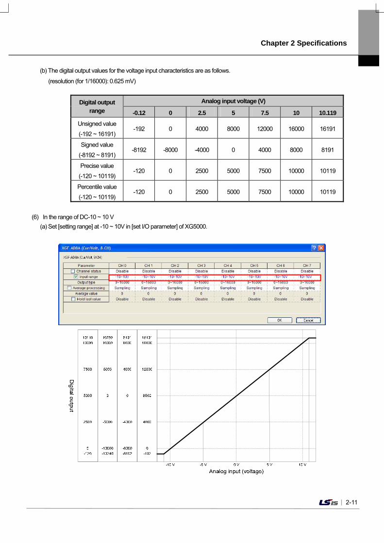
(6) In the range of DC-10 ~ 10 V
(a) Set [setting range] at -10 ~ 10V in [set I/O parameter] of XG5000.
Chapter 2 Specifications
2-12
(b) The digital output values for the voltage input characteristics are as follows.
(resolution (for 1/16000): 1.25 mV)
Digital output range
Analog input voltage (V)
-10.24 -10 -5 0 5 10 10.23
Unsigned value
(-192 ~ 16191) -192 0 4000 8000 12000 16000 16191
Signed value
(-8192 ~ 8191) -8192 -8000 -4000 0 4000 8000 8191
Precise value
(-10240 ~ 10239) -10240 0 2500 5000 7500 10000 10239
Percentile value
(-120 ~ 10119) -120 0 2500 5000 7500 10000 10119
Note
(1) When a value out of the digital output range is inputted as the analog input value, the digital output value is maintained as the maximum or the minimum value that fall within the set output range. For example, when the digital output range is set as the Unsigned value (–192 ~ 16191), and an analog value that exceed 6191 or -192 is entered as the digital output value, the digital output value is fixed at 16191 or -192. (2) The offset/gain of the analog input module cannot be set by the user.
Do not put the voltage and current beyond ±15 V and ±30 respectively. Otherwise it may cause a failure due to
over current/voltage.
Caution
Chapter 2 Specifications
2-13
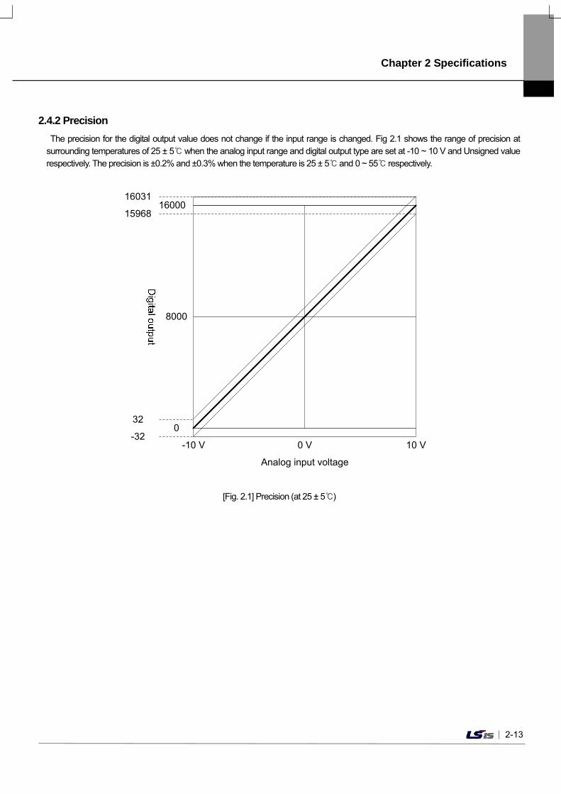
2.4.2 Precision The precision for the digital output value does not change if the input range is changed. Fig 2.1 shows the range of precision at
surrounding temperatures of 25 ± 5 when the analog input range and digital output type are set at -10 ~ 10 V and Unsigned value respectively. The precision is ±0.2% and ±0.3% when the temperature is 25 ± 5 and 0 ~ 55 respectively.
0
-10 V 0 V
8000
10 V
16000
Analog input voltage
15968
16031
-32
32
[Fig. 2.1] Precision (at 25 ± 5)
Chapter 2 Specifications
2-14
[Table 2.3] explains the functions of the analog conversion module.
[Table 2.3] List of functions
Functions Description Reference
Set channel operating/stop
Sets the operating/stop of the channel to conduct A/D conversion. You can reduce the time it takes for analog conversion by setting the channel you don’t use at stop.
Set input voltage/current ranges
Sets the analog input range you want to use. There are 4 input ranges for voltage input, and 2 for current input.
Set the output data type Sets the digital output type. 4 output data types are provided in this module.
A/D conversion type
(1) Sampling When no A/D conversion type is specified
(2) Average time/number Outputs the A/D conversion value of the average frequency or time.
(3) Weighted average Slows a sudden change of the input value.
Detection of an input disconnection
If the analog input at 4 ~ 20 mA and 1 ~ 5 V is disconnected, it can be detected in the user program.
Hold last value (1) This function is supported at current input (4~20mA, 0~20mA) (2) When input signal exceeds the effective range, holds the last effective value.
2.5.4 5.3.7
Alarm function (1) Separate setting is not necessary (2) When input signal exceeds the effective range, relevant flag turns on to let the user know
2.5.5 5.1.1
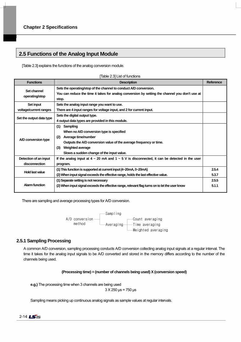
There are sampling and average processing types for A/D conversion.
A/D conversion method
Sampling
Averaging
Weighted averaging
Count averaging
Time averaging
2.5.1 Sampling Processing A common A/D conversion, sampling processing conducts A/D conversion collecting analog input signals at a regular interval. The time it takes for the analog input signals to be A/D converted and stored in the memory differs according to the number of the channels being used.
(Processing time) = (number of channels being used) X (conversion speed) e.g.) The processing time when 3 channels are being used
3 X 250 µs = 750 μs
Sampling means picking up continuous analog signals as sample values at regular intervals.
2.5 Functions of the Analog Input Module
Chapter 2 Specifications
2-15
2.5.2 Average Processing The A/D conversion of a designated channel is conducted a set times or for a set time and the average of the sum is stored in the memory.
(1) Why is average processing used?
Abnormal analog input signals such as noise can be A/D converted to a value close to a normal analog input signal.
(2) Types of average processing
Average processing divides into time, count and weighted averages.
(a) Time average processing 1) Settable range: 16 ~ 16000 (ms) 2) The number of average processing processes within the set time is decided according to the number of the channels being
used when you use the time average.
Example 1) the number of channels being used: 1, set time: 16000 ms
회횟수처리평균 6400025.01
16000
ms
ms
Example 2) the number of channels being used: 8, set time: 4 ms
*1: If you do not set the time average within 4 ~ 16000, RUN LED flashes every second. If you want to keep RUN LED on, reset the time average within 4 ~ 16000 and switch the operating mode of the CPU module from STOP to RUN. If you want to end the error through modification, you must use the clear request flag (UXY.11.0).
*2: In case of an error of the time average value setting, the set value is saved as 4, which is the initial value. The time average is converted into the number average inside the analog input module. In this case, there can be a remainder as time is divided by (the number of channels being used X conversion speed). The remainder is dropped, and the number of average processing processes is (the number of channels being used X conversion speed)/(set time).
Example) When the number of channels being used is 5 and the set time is 151 ms,
151 ms ÷ (5 X 0.25 ms) = 120 times …… the remainder is 8 120 times
(b) Count average processing 1) Settable range: 2 ~ 64000 (times) 2) When you use the number average, the times it takes for the average value to be saved in the memory differs according to
the number of the channels being used.
The processing time = the set number X the number of the channels being used X conversion speed
회횟수처리평균 225.08
4
ms
ms
Averaging Frequency Set-up time
No. channels used Conversion speed
Averaging Frequency 64000 Times
Averaging Frequency 2 Times
Chapter 2 Specifications
2-16
*1: If you do not set the time average within 2 ~ 64000, RUN LED flashes every second. If you want to keep RUN LED on, reset the time average within 2 ~ 64000 and switch the operating mode of the CPU module from STOP to RUN. If you want to end the error through modification, you must use the error clear request flag (UXY.11.0).
*2: In case of an error of the number average value setting, the set value is saved as 2, which is the initial value.
Example) when the number of channels being used 4 and the number of average processing processes is 50 times, 50 X 4 X (0.25 ms) = 50 ms
(c) Weighted average processing
Weighted average processing is for getting stable digital output values by filtering sudden changes of the noise or input values. The weighted average constant can be set for each channel by setting the user program or I/O parameter.
1) Settable range: 1 ~ 99(%)
F[n] = (1 - α) x A[n] + α x F [n - 1] F[n]: the current weighted average output value A[n]: the current A/D conversion value F[n-1]: the previous weighted average output value α: weighted average constant (0.01 ~ 0.99: weighted value of the previous value)
a) If you do not set the time average within 1~99, RUN LED flashes every second. If you want to keep RUN LED on, reset the time average within 4 ~ 16000 and switch the operating mode of the CPU module from STOP to RUN. If you want to end the error through modification, you must use the clear request flag (UXY.11.0).
b) In case of an error of the number average value setting, the set value is saved as 1, which is the initial value.
2) Voltage input a) The analog input range is set at DC -10 ~ 10 V and the digital output range is set at 0 ~ 16000.
b) When the analog input value changes –10 V 10 V (0 16000), the weighted average output value according to is as follows.
value Weighted average output value
Note - 1 scan 2 scans 3 scans
*1) 0.01 0 15840 15998 15999 1% biased toward previous value
*2) 0.5 0 8000 12000 14000 50% biased toward previous value
*3) 0.99 0 160 318 475 99% biased toward previous value
*1) 16000 output after about 4 scans *2) 16000 output after about 24 scans *3) 16000 output after about 1491 scans (372.75 ms in case of 1 channel operation)
3) Current input
a) The analog input range is set at DC 0 ~ 20 mA and the digital output range is set at 0 ~ 16000.
b) When the analog input value changes 0 mA 10 mA (0 8000), the weighted average output value according to is as follows
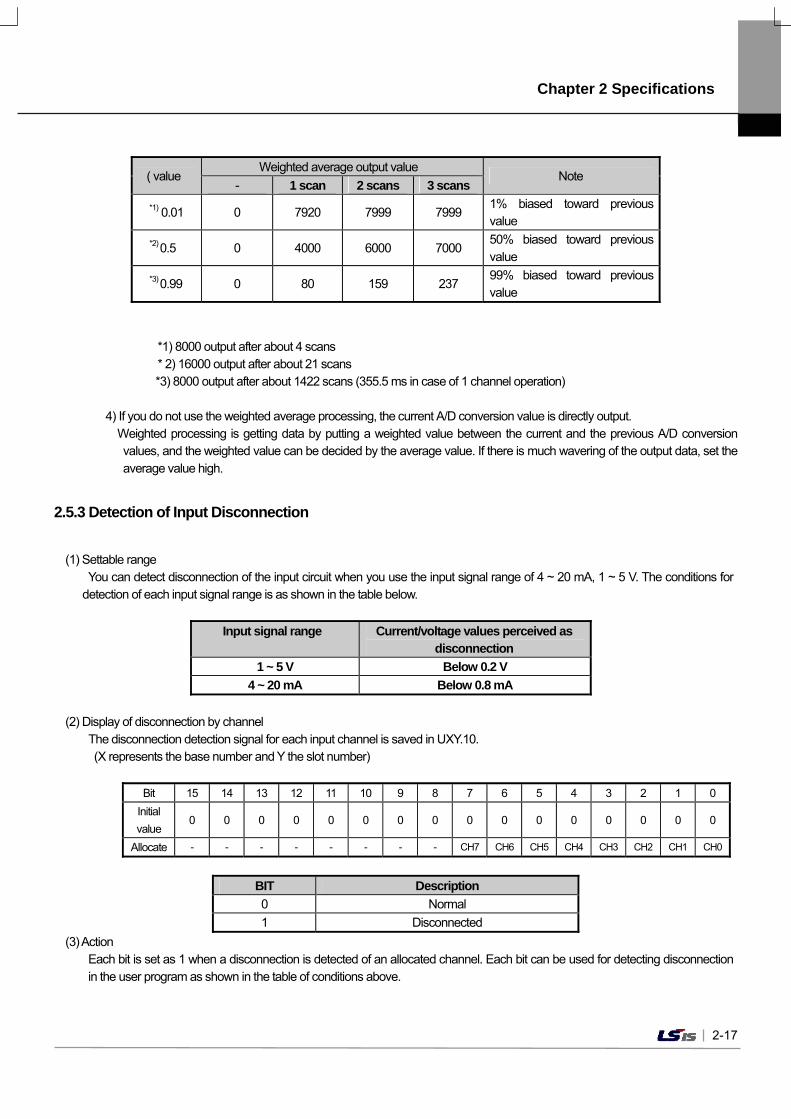
Chapter 2 Specifications
2-17
( value Weighted average output value
Note - 1 scan 2 scans 3 scans
*1) 0.01 0 7920 7999 7999 1% biased toward previous value
*2) 0.5 0 4000 6000 7000 50% biased toward previous value
*3) 0.99 0 80 159 237 99% biased toward previous value
*1) 8000 output after about 4 scans * 2) 16000 output after about 21 scans *3) 8000 output after about 1422 scans (355.5 ms in case of 1 channel operation)
4) If you do not use the weighted average processing, the current A/D conversion value is directly output. Weighted processing is getting data by putting a weighted value between the current and the previous A/D conversion
values, and the weighted value can be decided by the average value. If there is much wavering of the output data, set the average value high.
2.5.3 Detection of Input Disconnection
(1) Settable range
You can detect disconnection of the input circuit when you use the input signal range of 4 ~ 20 mA, 1 ~ 5 V. The conditions for detection of each input signal range is as shown in the table below.
Input signal range Current/voltage values perceived as disconnection
1 ~ 5 V Below 0.2 V 4 ~ 20 mA Below 0.8 mA
(2) Display of disconnection by channel
The disconnection detection signal for each input channel is saved in UXY.10. (X represents the base number and Y the slot number)
Bit 15 14 13 12 11 10 9 8 7 6 5 4 3 2 1 0
Initial
value 0 0 0 0 0 0 0 0 0 0 0 0 0 0 0 0
Allocate - - - - - - - - CH7 CH6 CH5 CH4 CH3 CH2 CH1 CH0
BIT Description 0 Normal
1 Disconnected
(3) Action Each bit is set as 1 when a disconnection is detected of an allocated channel. Each bit can be used for detecting disconnection in the user program as shown in the table of conditions above.
Chapter 2 Specifications
2-18
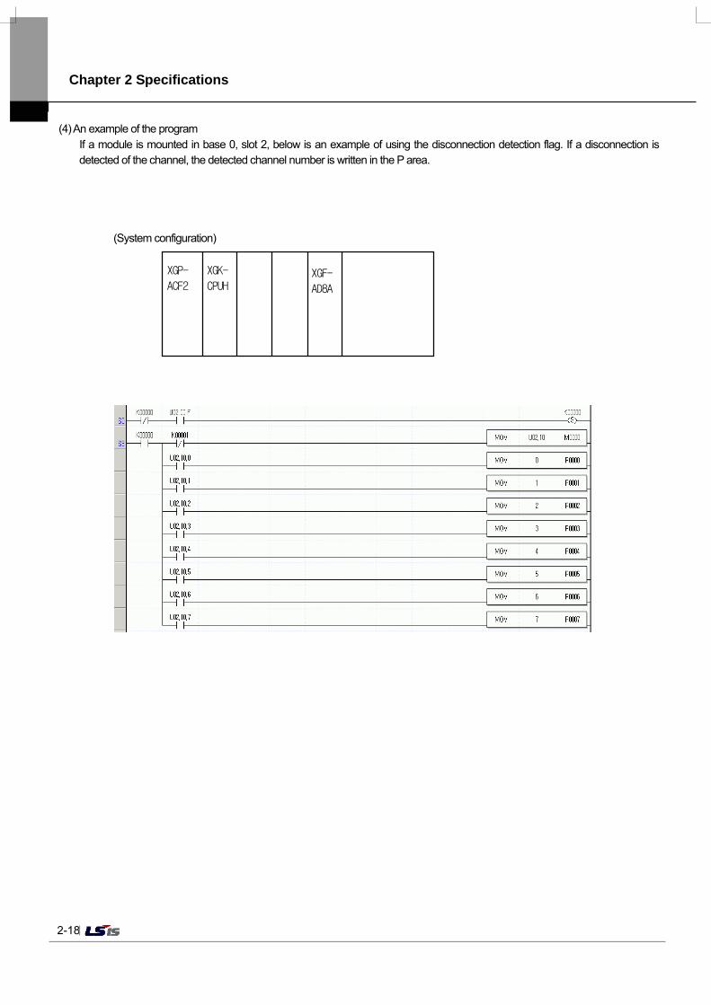
(4) An example of the program If a module is mounted in base 0, slot 2, below is an example of using the disconnection detection flag. If a disconnection is detected of the channel, the detected channel number is written in the P area.
(System configuration)
XGP-
ACF2
XGK-
CPUH
XGF-
AD8A
Chapter 2 Specifications
2-19
2.5.4 Hold last value (Dedicated for current input) When input signal exceeds the effective range, last input value is held. This function can be set for each channel by I/O
parameter setting or user program.
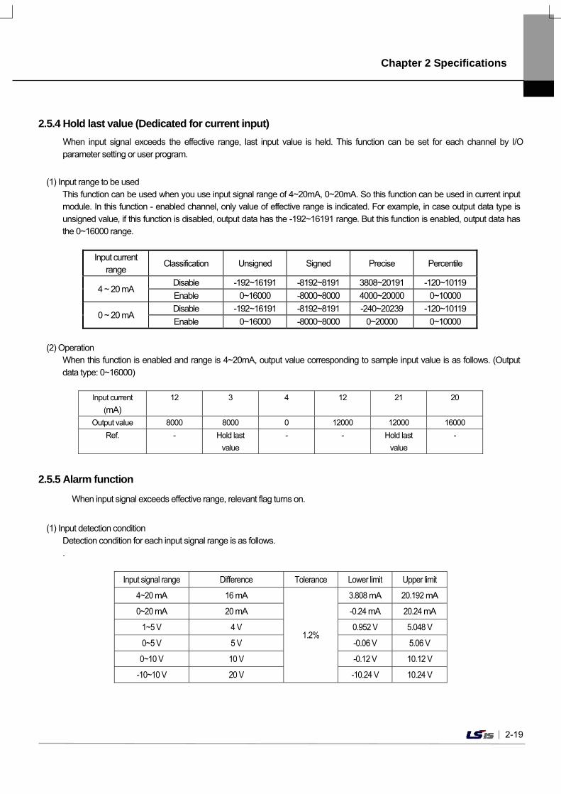
(1) Input range to be used
This function can be used when you use input signal range of 4~20mA, 0~20mA. So this function can be used in current input module. In this function - enabled channel, only value of effective range is indicated. For example, in case output data type is unsigned value, if this function is disabled, output data has the -192~16191 range. But this function is enabled, output data has the 0~16000 range.
Input current range
Classification Unsigned Signed Precise Percentile
4 ~ 20 mA Disable -192~16191 -8192~8191 3808~20191 -120~10119
Enable 0~16000 -8000~8000 4000~20000 0~10000
0 ~ 20 mA Disable -192~16191 -8192~8191 -240~20239 -120~10119
Enable 0~16000 -8000~8000 0~20000 0~10000
(2) Operation
When this function is enabled and range is 4~20mA, output value corresponding to sample input value is as follows. (Output data type: 0~16000)
Input current
(mA)
12 3 4 12 21 20
Output value 8000 8000 0 12000 12000 16000
Ref. - Hold last
value
- - Hold last
value
-
2.5.5 Alarm function
When input signal exceeds effective range, relevant flag turns on.
(1) Input detection condition Detection condition for each input signal range is as follows. .
Input signal range Difference Tolerance Lower limit Upper limit
4~20 mA 16 mA
1.2%
3.808 mA 20.192 mA
0~20 mA 20 mA -0.24 mA 20.24 mA
1~5 V 4 V 0.952 V 5.048 V
0~5 V 5 V -0.06 V 5.06 V
0~10 V 10 V -0.12 V 10.12 V
-10~10 V 20 V -10.24 V 10.24 V
Chapter 2 Specifications
2-20
(2) Alarm indication for each channel
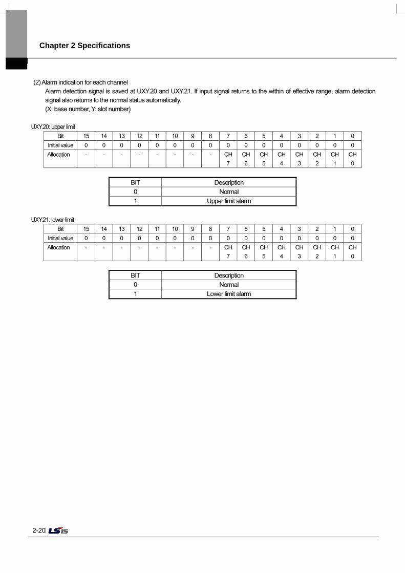
Alarm detection signal is saved at UXY.20 and UXY.21. If input signal returns to the within of effective range, alarm detection signal also returns to the normal status automatically. (X: base number, Y: slot number)
UXY.20: upper limit
Bit 15 14 13 12 11 10 9 8 7 6 5 4 3 2 1 0
Initial value 0 0 0 0 0 0 0 0 0 0 0 0 0 0 0 0
Allocation - - - - - - - - CH
7
CH
6
CH
5
CH
4
CH
3
CH
2
CH
1
CH
0
BIT Description
0 Normal
1 Upper limit alarm
UXY.21: lower limit
Bit 15 14 13 12 11 10 9 8 7 6 5 4 3 2 1 0
Initial value 0 0 0 0 0 0 0 0 0 0 0 0 0 0 0 0
Allocation - - - - - - - - CH
7
CH
6
CH
5
CH
4
CH
3
CH
2
CH
1
CH
0
BIT Description
0 Normal
1 Lower limit alarm
Chapter 3 Installation and Wiring
3-1
Chapter 3 Installation and Wiring
3.1 Installation
3.1.1 Installation Environment Although this device has high reliability regardless of the environment where it is mounted, pay attention to the following conditions for reliability and stability of the system.
(1) Environment conditions (a) Mount on a water-proof and vibration proof controlling board. (b) Where there are no continuous shocks or vibrations (c) Where there is no direct sunlight (d) Where there is no condensation caused by sudden changes of the temperature (e) Where the temperature remains between 0-55
(2) Installation work (a) Do not leave wiring remnants in the PLC when boring screw holes or doing wiring work. (b) Install in a place where you can easily manipulate it. (c) Do not install with a high voltage device in the same panel (d) Keep at least 50mm from a duct or module. (e) Connect to ground where the noise environment is good.
3.1.2 Precautions in Handling This section provides information on the precautions in from opening to installing the analog conversion module.
(1) Do not drop or hit hard.
(2) Do not separate the PCB from the case. It may cause a failure.
(3) Be careful not to let foreign substances such as the wiring remnants in the upper part of the module when doing the wiring work.
(4) Do not mount or dismount when the power is on.
Chapter 3 Installation and Wiring
3-2
3.2 Wiring
3.2.1 Precautions in Wiring
(1) Do not put an AC power supply line near an external input signal line of an analog input module. Keep them apart enough not to
be affected by the surge or induced noise from the AC side.
(2) Consider the surrounding temperature and allowed current when choosing the cable. A cable should be larger in maximum
diameter than AWG22(0.3).
(3) If the cable is placed too close to a hot device or material or put in direct contact with oil, for example, it may cause a
short circuit and result in damage or malfunction.
(4) Check the polarity when wiring the terminal block.
(5) When cables are wired with high voltage lines or power supply cords, an induction failure may occur resulting in
malfunction or a failure.
3.2.2 An Example of Wiring
(1) Voltage inputs
+
R
-
CH0
CH7 +
-
R
R
R*3
*3
*1
*1
+
-
+
-
(2) Current inputs
+
R
-
CH0
CH7 +
-
R
R
R*3R
R
*2
*2 *3
+
-
+
-
*1
*1
*1) Use 2 core twist shield cable. AWG 22 is recommended for the size of the cable. *2) 250 Ω (typ.) as the current input resistance of the analog input module. *3) 1 MΩ (min.) as the voltage input resistance of the analog input module.
Chapter 3 Installation and Wiring
3-3
(3) An example of 2-wire sensor/transmitter wiring (current inputs)
+
R
2-Wire Transmitter
2-Wire Transmitter
-
CH0
CH7 +
-
R
R
RDC
+
-
DC+
-
*3R
R
*2
*2 *3
*1
*1
(a) Set only the channel you are using at channel operation. (b) The analog input module does not supply the power for an input device. Use an external power supply.
(4) An example of 4-wire sensor/transmitter wiring (voltage and current inputs)
+
R
4-Wire Transmitter
4-Wire Transmitter
-
CH0
CH7 +
-
R
R
RDC
+
-
DC+
-
*3R
R
*2
*2 *3
*1
*1
(a) Set only the channel you are using at channel operation. (b) The analog input module does not supply the power for an input device. Use an external power supply.
*1) Use 2 core twist shield cable. AWG 22 is recommended for the size of the cable. *2) 250 Ω (typ.) as the current input resistance of the analog input module. *3) 1 MΩ (min.) as the voltage input resistance of the analog input module.
Chapter 3 Installation and Wiring
3-4
(5) The relation between the voltage input precision and wiring length The wiring length between the transmitter or sensor and the module in voltage inputs affect the digital conversion values of the module as shown below.
In the figure, Rc: the loop resistance of the cable
Rs: the internal resistance of the transmitter or sensor Ri: the internal resistance of the module (1) when the voltage is input Vin: the voltage supplied to the analog input module % Vi: the error (%) of the conversion values resulting from the source and cable lengths in voltage inputs
( )[ ]RiRcRsVsRiVin
+×+×
=2
1001% ×
−=
VsVinVi %
Note
There is no precision error from the cable length and the internal resistance of the source in current inputs.
Vs
Rs Rc
Rc
Ri
Load
Analog input (voltage)
Vin
`
Chapter 4 Operating Setting
4-1
Chapter 4 Operating Setting
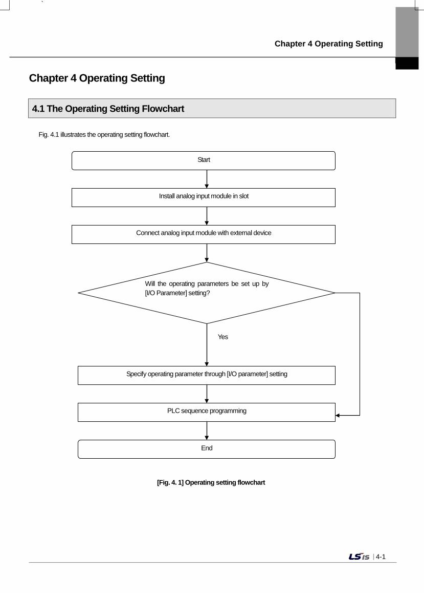
4.1 The Operating Setting Flowchart Fig. 4.1 illustrates the operating setting flowchart.
[Fig. 4. 1] Operating setting flowchart
Start
Install analog input module in slot
Connect analog input module with external device
Specify operating parameter through [I/O parameter] setting
PLC sequence programming
End
Will the operating parameters be set up by [I/O Parameter] setting?
Yes

Chapter 4 Operating Setting
4-2
4.2 Operating Parameter Setting
The operating parameters of the analog input module can be set in [I/O parameter] of XG 5000.
4.2.1 Setting Items XG5000 provides GUI (Graphical User Interface) type parameter setting of the analog input module in order to enhance the user’s convenience. Table 4.1 shows the parameters that can be set through [I/O parameter] in the project window of XG5000.
[Table 4. 1] Functions of [I/O parameter]
Description
[I/O parameter] (1) The following items are set that are necessary for operating the module.
(a) channel run/stop
(b) analog input range
(c) digital output data type
(d) average processing method
(e) average value
(2) The data set by the user in XG5000 is stored in the analog input module when
[I/O parameter] is downloaded. That is, when [I/O parameter] is stored in the
analog input module is not related to the RUN or STOP of PLC CPU.
4.2.2 How to Use [I/O Parameter] (1) Start XG5000 and create a project.
(For how to create a project, see the program manual of XG5000) (2) Double-click on [I/O parameter] in the project window.
`
Chapter 4 Operating Setting
4-3
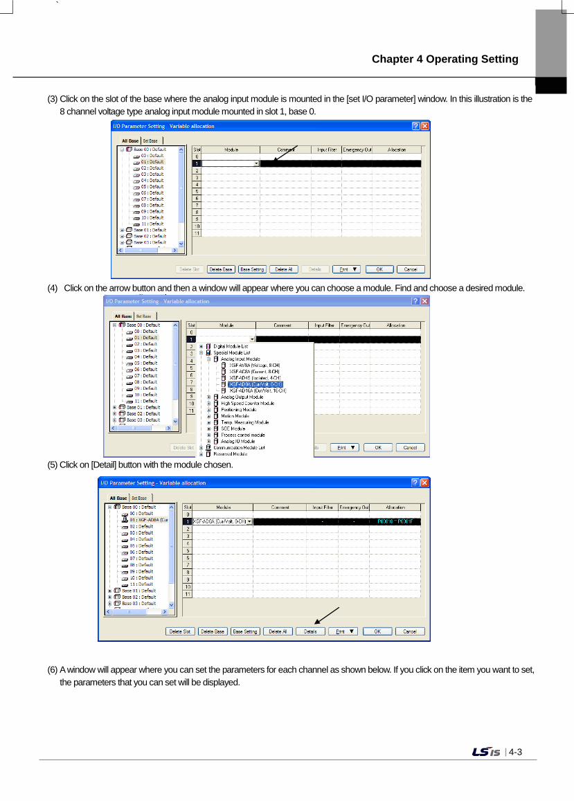
(3) Click on the slot of the base where the analog input module is mounted in the [set I/O parameter] window. In this illustration is the 8 channel voltage type analog input module mounted in slot 1, base 0.
(4) Click on the arrow button and then a window will appear where you can choose a module. Find and choose a desired module.
(5) Click on [Detail] button with the module chosen.
(6) A window will appear where you can set the parameters for each channel as shown below. If you click on the item you want to set,
the parameters that you can set will be displayed.
Chapter 4 Operating Setting
4-4
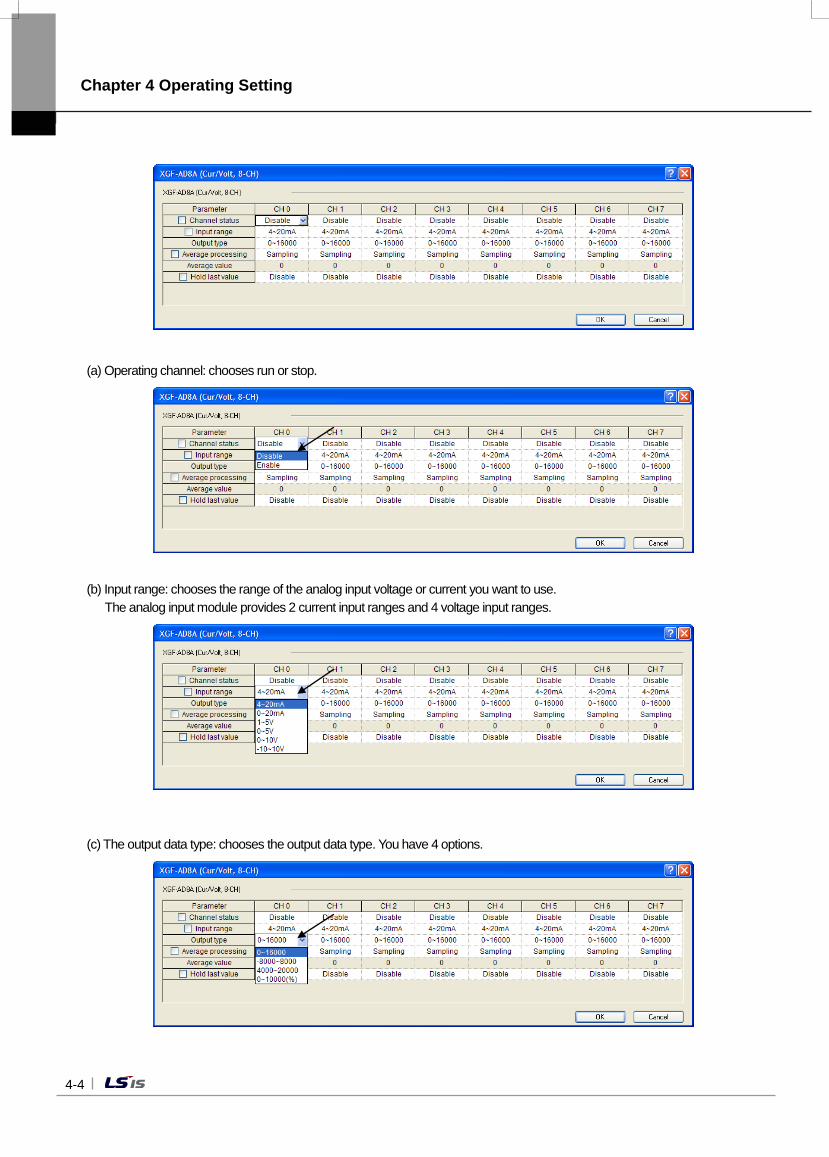
(a) Operating channel: chooses run or stop.
(b) Input range: chooses the range of the analog input voltage or current you want to use. The analog input module provides 2 current input ranges and 4 voltage input ranges.
(c) The output data type: chooses the output data type. You have 4 options.
`
Chapter 4 Operating Setting
4-5
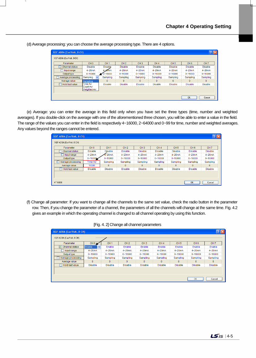
(d) Average processing: you can choose the average processing type. There are 4 options.
(e) Average: you can enter the average in this field only when you have set the three types (time, number and weighted
averages). If you double-click on the average with one of the aforementioned three chosen, you will be able to enter a value in the field. The range of the values you can enter in the field is respectively 4~16000, 2~64000 and 0~99 for time, number and weighted averages. Any values beyond the ranges cannot be entered.
(f) Change all parameter: If you want to change all the channels to the same set value, check the radio button in the parameter
row. Then, if you change the parameter of a channel, the parameters of all the channels will change at the same time. Fig. 4.2 gives an example in which the operating channel is changed to all channel operating by using this function.
[Fig. 4. 2] Change all channel parameters
Chapter 4 Operating Setting
4-6
4.3 Functions of the Special Module Monitor
Table 4.3 shows the functions of the special module monitor.
[Table 4.3] The functions of the special module monitor
Item Description Note [Special module monitor]
(1) Monitor/test You can monitor the A/D conversion value or test the operating of the analog input module through the menu connected to [Monitor] of XG5000 -> [Special module monitor].
(2) Minimum/maximum monitor You can monitor the minimum and maximum values of a running channel. The values you can see are the current values displayed on the screen. Therefore the minimum and maximum values are not saved when you close the [Monitoring/test] window.
-
Note
If there are not enough system resources of the PC you are using, the display may not be normally functioning. In such a case, close the window, end other applications and restart XG5000.
`
Chapter 4 Operating Setting
4-7
4.4 Precautions
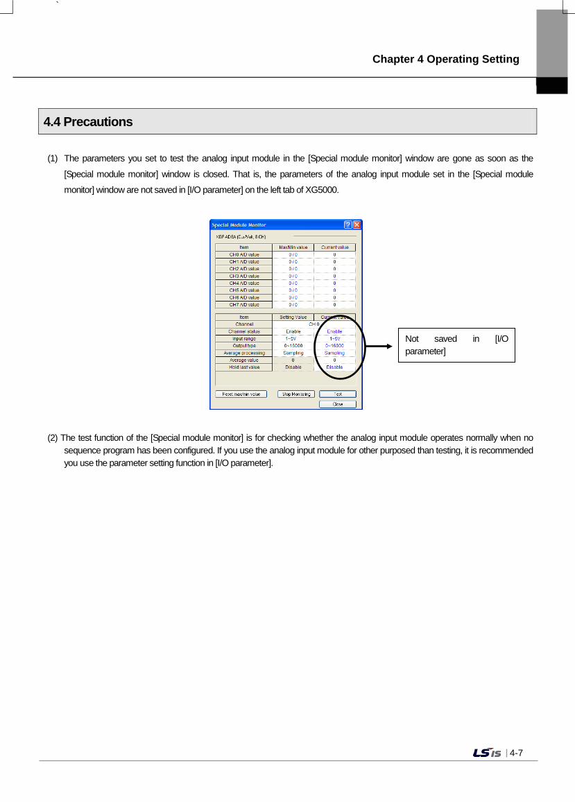
(1) The parameters you set to test the analog input module in the [Special module monitor] window are gone as soon as the
[Special module monitor] window is closed. That is, the parameters of the analog input module set in the [Special module
monitor] window are not saved in [I/O parameter] on the left tab of XG5000.
(2) The test function of the [Special module monitor] is for checking whether the analog input module operates normally when no
sequence program has been configured. If you use the analog input module for other purposed than testing, it is recommended you use the parameter setting function in [I/O parameter].
Not saved in [I/O parameter]
Chapter 4 Operating Setting
4-8
4.5 How to Use the Special Module Monitor
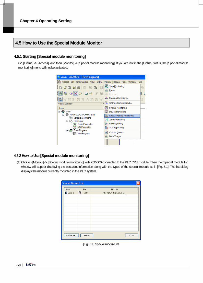
4.5.1 Starting [Special module monitoring] Go [Online] -> [Access], and then [Monitor] -> [Special module monitoring]. If you are not in the [Online] status, the [Special module monitoring] menu will not be activated.
4.5.2 How to Use [Special module monitoring] (1) Click on [Monitor] -> [Special module monitoring] with XG5000 connected to the PLC CPU module. Then the [Special module list]
window will appear displaying the base/slot information along with the types of the special module as in [Fig. 5.1]. The list dialog displays the module currently mounted in the PLC system.
[Fig. 5.1] Special module list
`
Chapter 4 Operating Setting
4-9
(2) Select the special module and click on [Module information] in Fig. 5.1., and then the [Special module information] will appear as in Fig. 5.2.
[Fig. 5.2] [Select module information]
(3) Click on the [Monitor] button in the [Special module list] in Fig. 5.1, and then the [Special module monitor] window will appear as in
[Fig. 5.3]. There are 4 buttons of [Reset max/min], [Start monitoring], [Start test] and [Close] in this window. The monitor at the top of the screen displays the outputs of the analog input module and maximum/minimum values. In the test window at the bottom of the screen, you can configure the parameter items discretely of each module.
[Fig. 5.3] [Special module monitor]
Chapter 4 Operating Setting
4-10
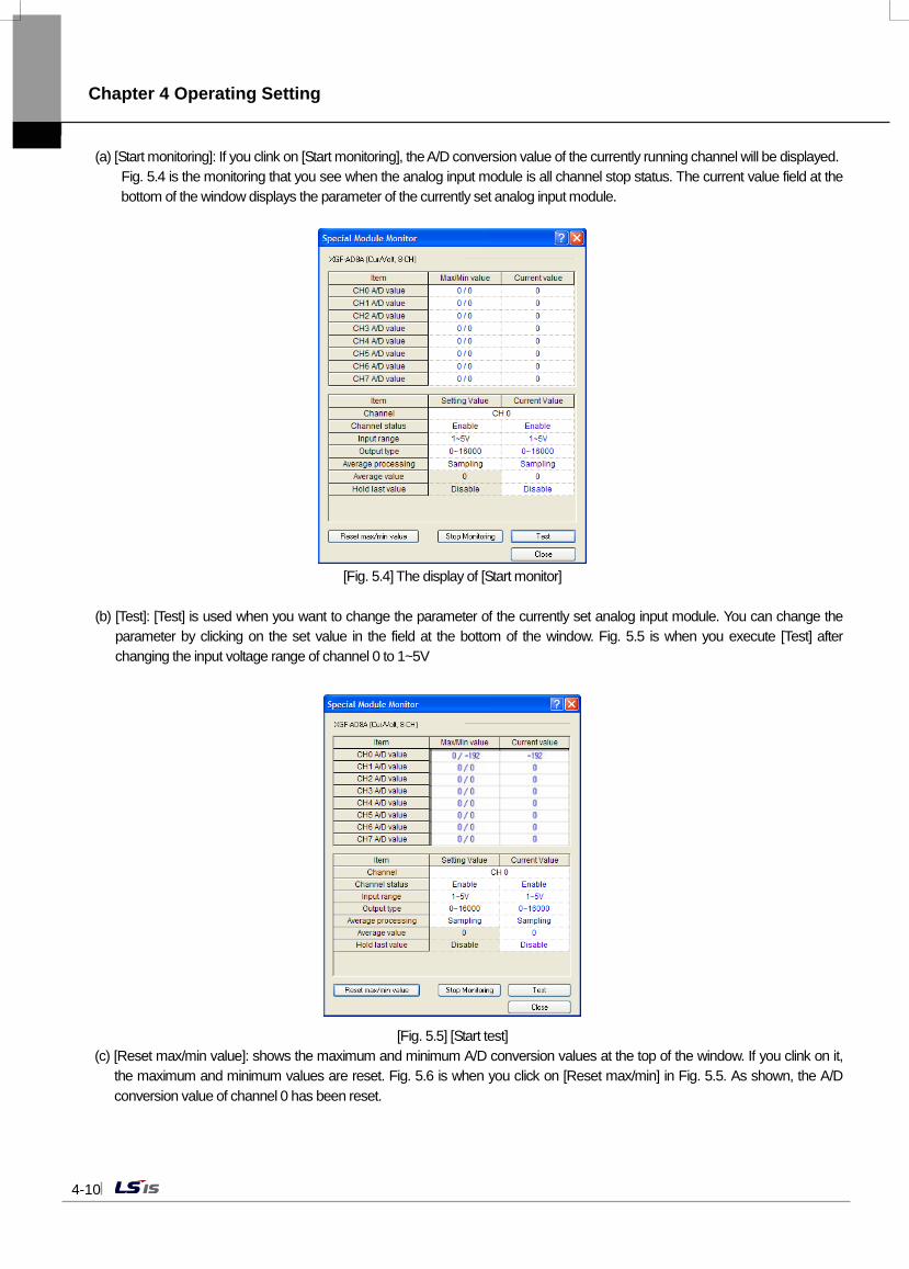
(a) [Start monitoring]: If you clink on [Start monitoring], the A/D conversion value of the currently running channel will be displayed. Fig. 5.4 is the monitoring that you see when the analog input module is all channel stop status. The current value field at the bottom of the window displays the parameter of the currently set analog input module.
[Fig. 5.4] The display of [Start monitor]
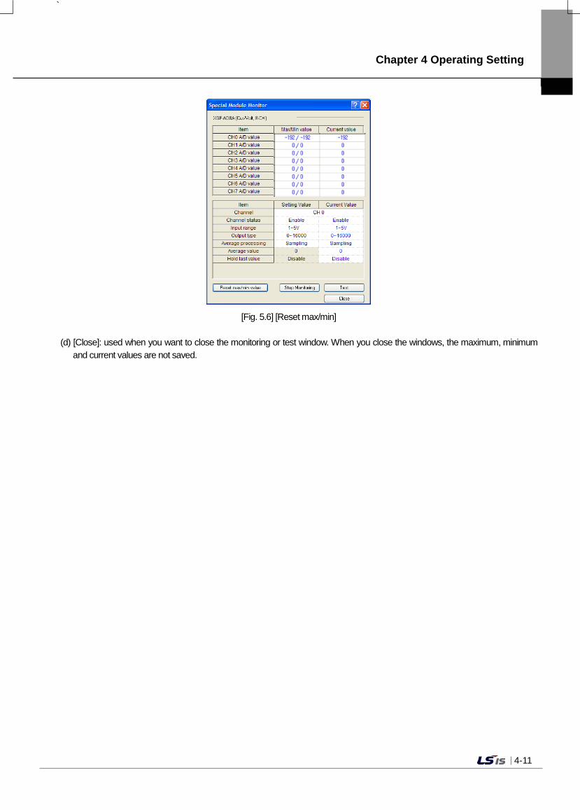
(b) [Test]: [Test] is used when you want to change the parameter of the currently set analog input module. You can change the
parameter by clicking on the set value in the field at the bottom of the window. Fig. 5.5 is when you execute [Test] after changing the input voltage range of channel 0 to 1~5V
[Fig. 5.5] [Start test]
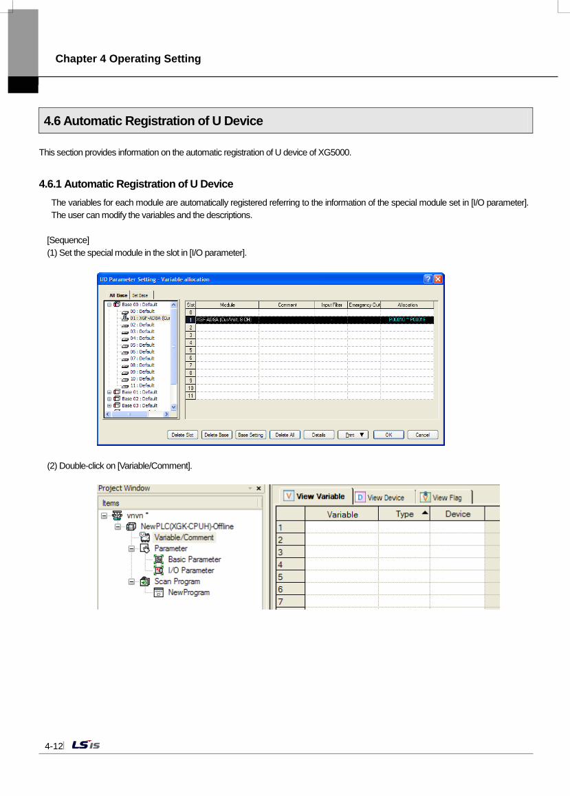
(c) [Reset max/min value]: shows the maximum and minimum A/D conversion values at the top of the window. If you clink on it, the maximum and minimum values are reset. Fig. 5.6 is when you click on [Reset max/min] in Fig. 5.5. As shown, the A/D conversion value of channel 0 has been reset.
`
Chapter 4 Operating Setting
4-11
[Fig. 5.6] [Reset max/min]
(d) [Close]: used when you want to close the monitoring or test window. When you close the windows, the maximum, minimum
and current values are not saved.
Chapter 4 Operating Setting
4-12
4.6 Automatic Registration of U Device This section provides information on the automatic registration of U device of XG5000.
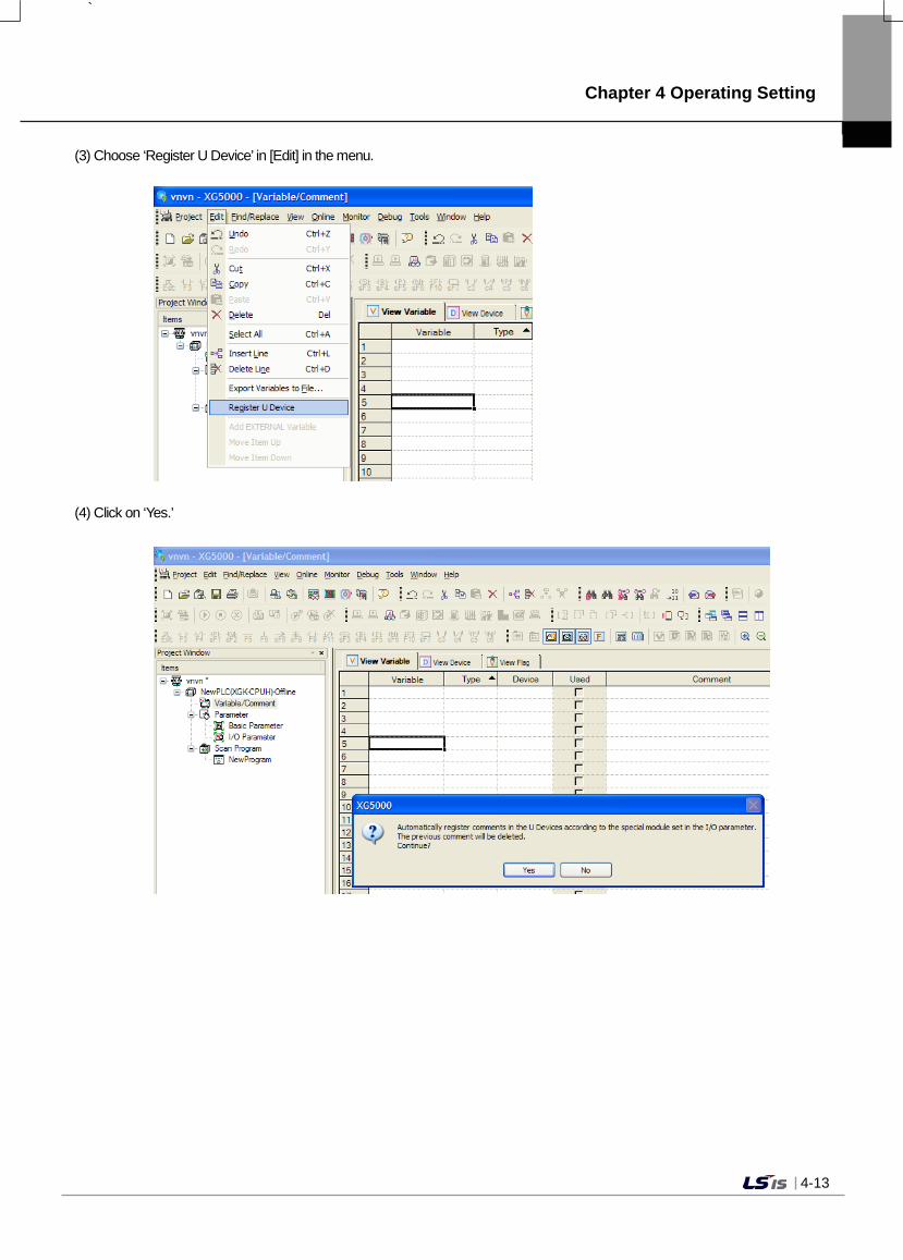
4.6.1 Automatic Registration of U Device The variables for each module are automatically registered referring to the information of the special module set in [I/O parameter]. The user can modify the variables and the descriptions.
[Sequence] (1) Set the special module in the slot in [I/O parameter].
(2) Double-click on [Variable/Comment].
`
Chapter 4 Operating Setting
4-13
(3) Choose ‘Register U Device’ in [Edit] in the menu.
(4) Click on ‘Yes.’
Chapter 4 Operating Setting
4-14
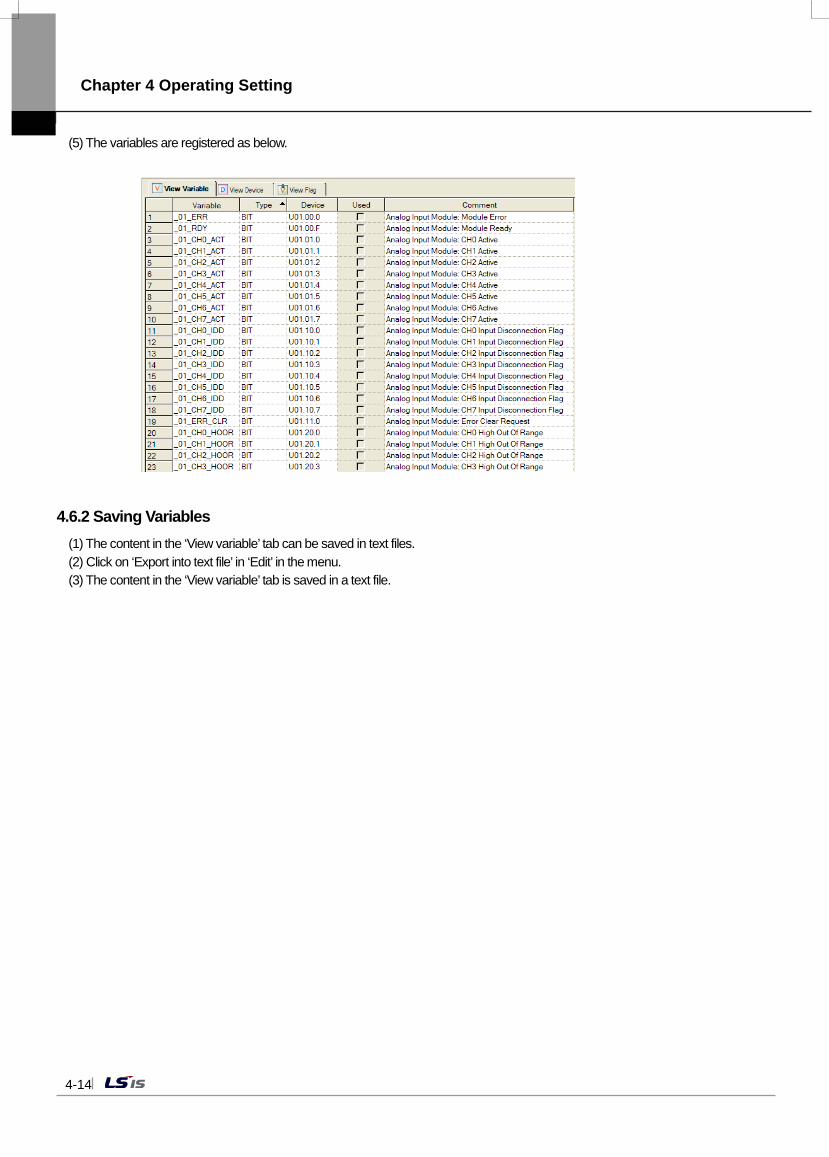
(5) The variables are registered as below.
4.6.2 Saving Variables (1) The content in the ‘View variable’ tab can be saved in text files. (2) Click on ‘Export into text file’ in ‘Edit’ in the menu. (3) The content in the ‘View variable’ tab is saved in a text file.
`
Chapter 4 Operating Setting
4-15
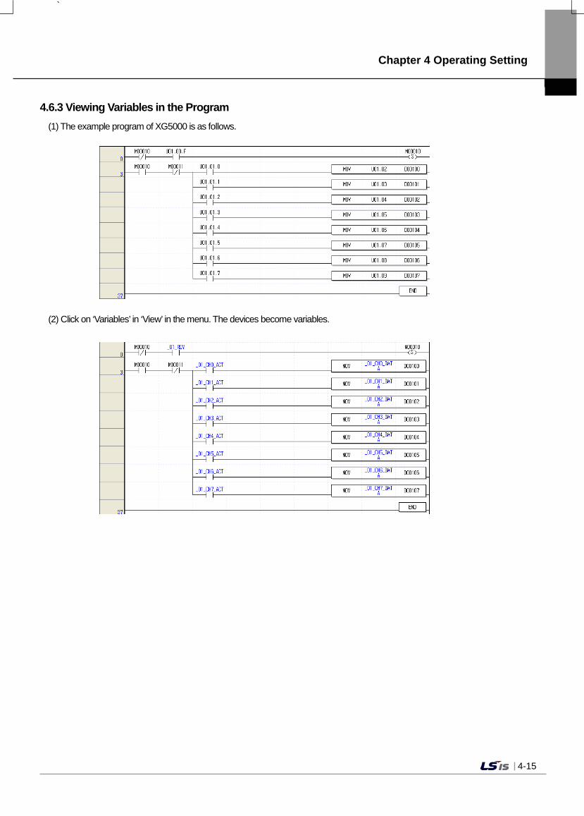
4.6.3 Viewing Variables in the Program (1) The example program of XG5000 is as follows.
(2) Click on ‘Variables’ in ‘View’ in the menu. The devices become variables.
Chapter 4 Operating Setting
4-16
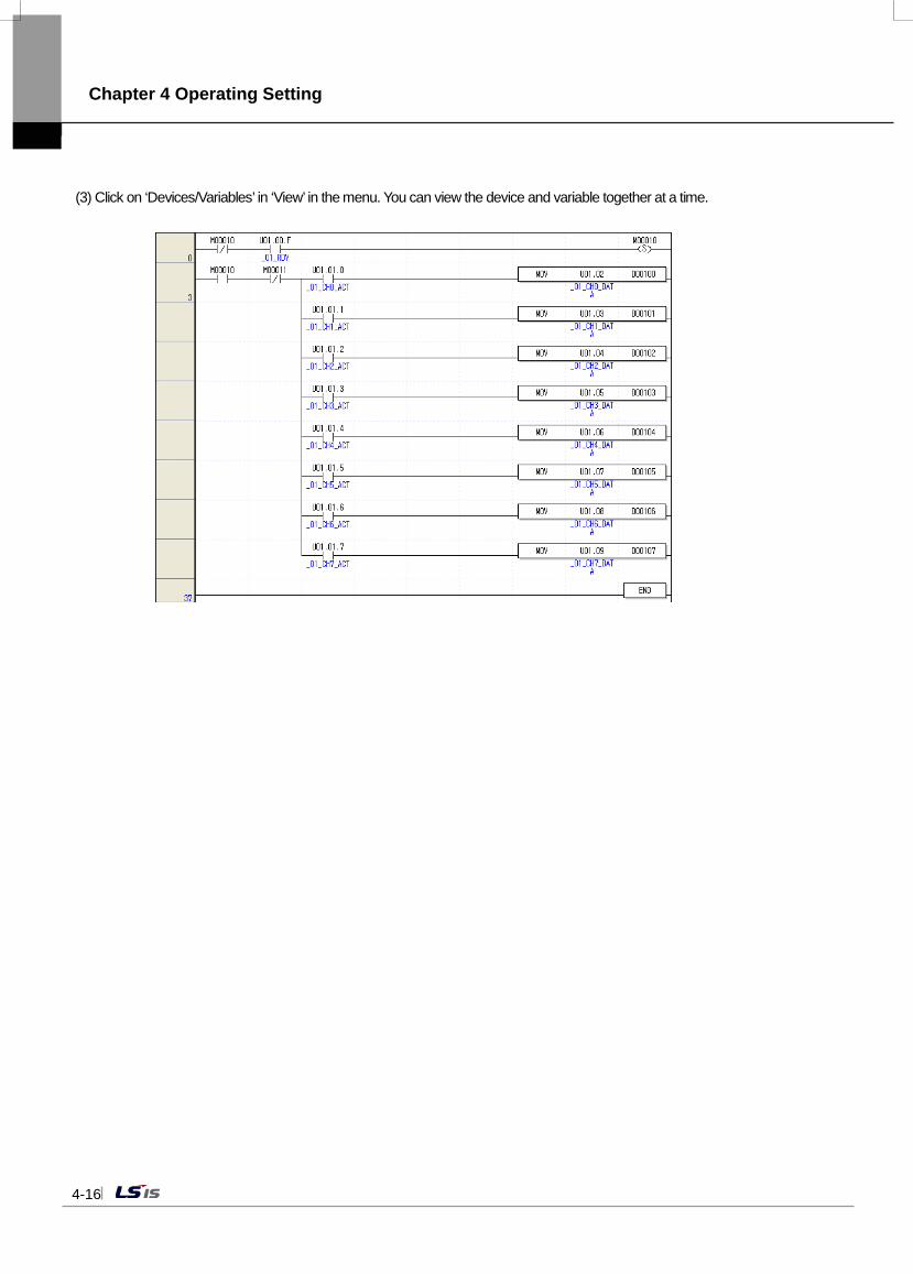
(3) Click on ‘Devices/Variables’ in ‘View’ in the menu. You can view the device and variable together at a time.
`
Chapter 4 Operating Setting
4-17
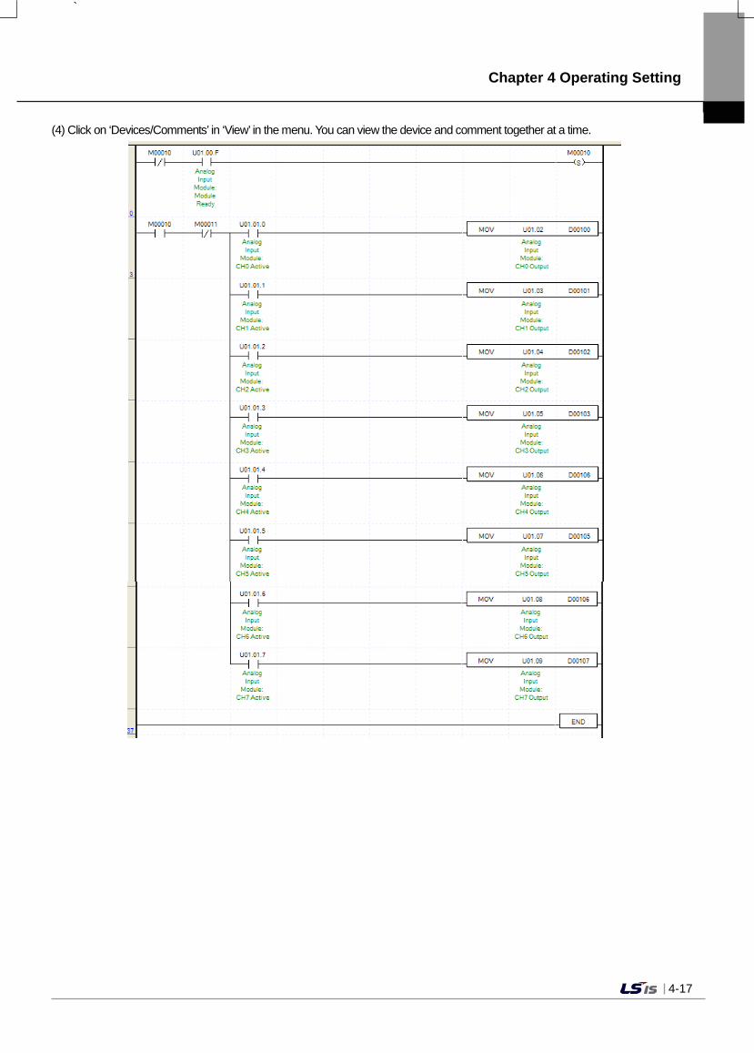
(4) Click on ‘Devices/Comments’ in ‘View’ in the menu. You can view the device and comment together at a time.
Chapter 4 Operating Setting
4-18
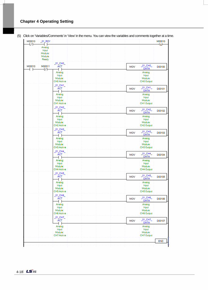
(5) Click on ‘Variables/Comments’ in ‘View’ in the menu. You can view the variables and comments together at a time.
Chapter 5 Configuration and Functions of the Internal Memory
5-1
Chapter 5 Configuration and Functions of the Internal Memory (XGK) The analog input module has an internal memory for transmitting and receiving data with the PLC CPU.
5.1 The Configuration of the Internal Memory This section gives information on the configuration of the internal memory.
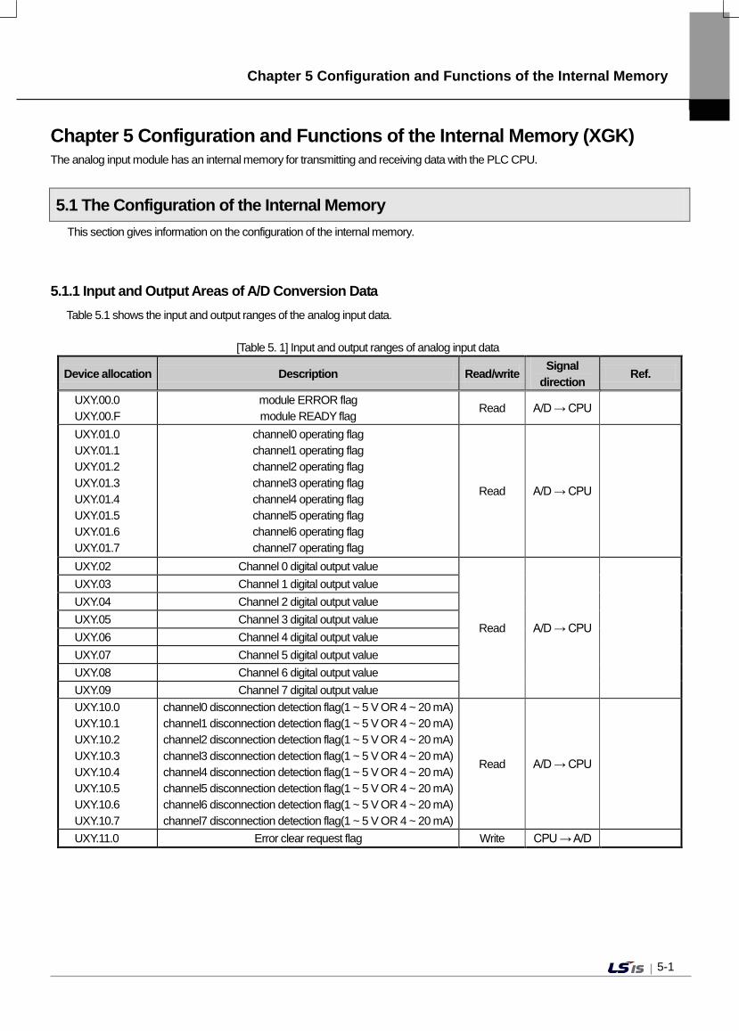
5.1.1 Input and Output Areas of A/D Conversion Data Table 5.1 shows the input and output ranges of the analog input data.
[Table 5. 1] Input and output ranges of analog input data
Device allocation Description Read/write Signal direction
Ref.
UXY.00.0 UXY.00.F
module ERROR flag module READY flag
Read A/D → CPU
UXY.01.0 UXY.01.1 UXY.01.2 UXY.01.3 UXY.01.4 UXY.01.5 UXY.01.6 UXY.01.7
channel0 operating flag channel1 operating flag channel2 operating flag channel3 operating flag channel4 operating flag channel5 operating flag channel6 operating flag channel7 operating flag
Read A/D → CPU
UXY.02 Channel 0 digital output value
Read A/D → CPU
UXY.03 Channel 1 digital output value UXY.04 Channel 2 digital output value UXY.05 Channel 3 digital output value UXY.06 Channel 4 digital output value UXY.07 Channel 5 digital output value UXY.08 Channel 6 digital output value UXY.09 Channel 7 digital output value UXY.10.0 UXY.10.1 UXY.10.2 UXY.10.3 UXY.10.4 UXY.10.5 UXY.10.6 UXY.10.7
channel0 disconnection detection flag(1 ~ 5 V OR 4 ~ 20 mA) channel1 disconnection detection flag(1 ~ 5 V OR 4 ~ 20 mA) channel2 disconnection detection flag(1 ~ 5 V OR 4 ~ 20 mA) channel3 disconnection detection flag(1 ~ 5 V OR 4 ~ 20 mA) channel4 disconnection detection flag(1 ~ 5 V OR 4 ~ 20 mA) channel5 disconnection detection flag(1 ~ 5 V OR 4 ~ 20 mA) channel6 disconnection detection flag(1 ~ 5 V OR 4 ~ 20 mA) channel7 disconnection detection flag(1 ~ 5 V OR 4 ~ 20 mA)
Read A/D → CPU
UXY.11.0 Error clear request flag Write CPU → A/D
Chapter 5 Configuration and Functions of the Internal Memory
5-2
Device allocation Description Read/write Signal direction Ref.
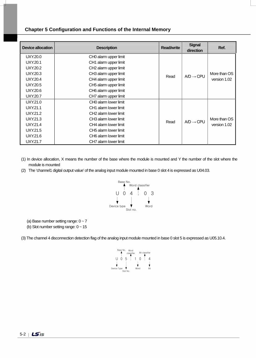
UXY.20.0 UXY.20.1 UXY.20.2 UXY.20.3 UXY.20.4 UXY.20.5 UXY.20.6 UXY.20.7
CH0 alarm upper limit CH1 alarm upper limit CH2 alarm upper limit CH3 alarm upper limit CH4 alarm upper limit CH5 alarm upper limit CH6 alarm upper limit CH7 alarm upper limit
Read A/D → CPU More than OS version 1.02
UXY.21.0 UXY.21.1 UXY.21.2 UXY.21.3 UXY.21.4 UXY.21.5 UXY.21.6 UXY.21.7
CH0 alarm lower limit CH1 alarm lower limit CH2 alarm lower limit CH3 alarm lower limit CH4 alarm lower limit CH5 alarm lower limit CH6 alarm lower limit CH7 alarm lower limit
Read A/D → CPU More than OS version 1.02
(1) In device allocation, X means the number of the base where the module is mounted and Y the number of the slot where the module is mounted
(2) The ‘channel1 digital output value’ of the analog input module mounted in base 0 slot 4 is expressed as U04.03.
Device type
Base No.
U 0 4 . 0 3
Slot no.
Word classifier
Word
(a) Base number setting range: 0 ~ 7 (b) Slot number setting range: 0 ~ 15
(3) The channel 4 disconnection detection flag of the analog input module mounted in base 0 slot 5 is expressed as U05.10.4.
Device Type
Base No.
U 0 5 . 1 0
Slot No.
Word classifier
Word
. 4
Bit classifier
Bit
Chapter 5 Configuration and Functions of the Internal Memory
5-3
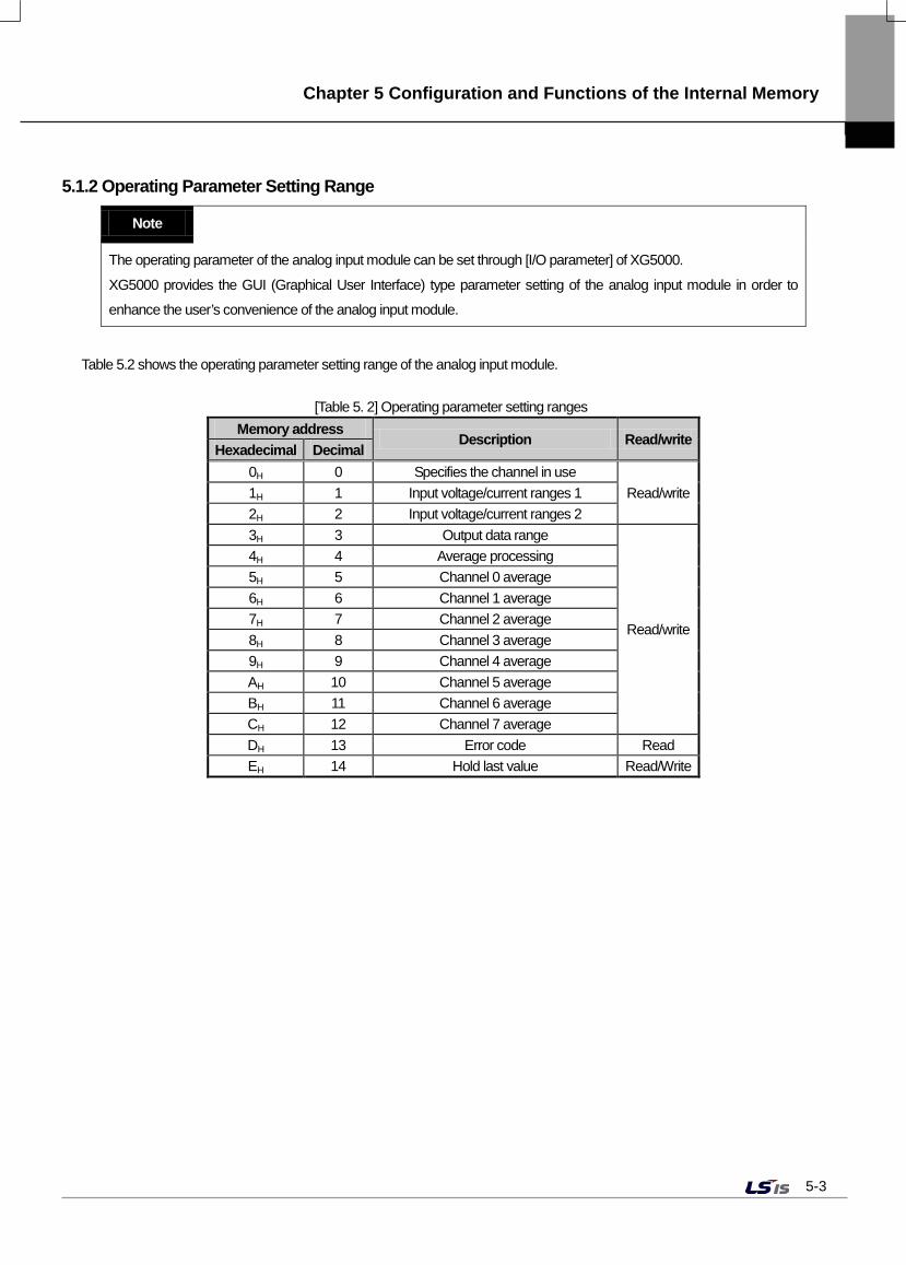
5.1.2 Operating Parameter Setting Range
Note
The operating parameter of the analog input module can be set through [I/O parameter] of XG5000.
XG5000 provides the GUI (Graphical User Interface) type parameter setting of the analog input module in order to
enhance the user’s convenience of the analog input module.
Table 5.2 shows the operating parameter setting range of the analog input module.
[Table 5. 2] Operating parameter setting ranges Memory address
Description Read/write Hexadecimal Decimal
0H 0 Specifies the channel in use Read/write 1H 1 Input voltage/current ranges 1
2H 2 Input voltage/current ranges 2 3H 3 Output data range
Read/write
4H 4 Average processing 5H 5 Channel 0 average 6H 6 Channel 1 average 7H 7 Channel 2 average 8H 8 Channel 3 average 9H 9 Channel 4 average AH 10 Channel 5 average BH 11 Channel 6 average CH 12 Channel 7 average DH 13 Error code Read EH 14 Hold last value Read/Write
Chapter 5 Configuration and Functions of the Internal Memory
5-4
5.2 A/D Conversion Data Input/Output Ranges
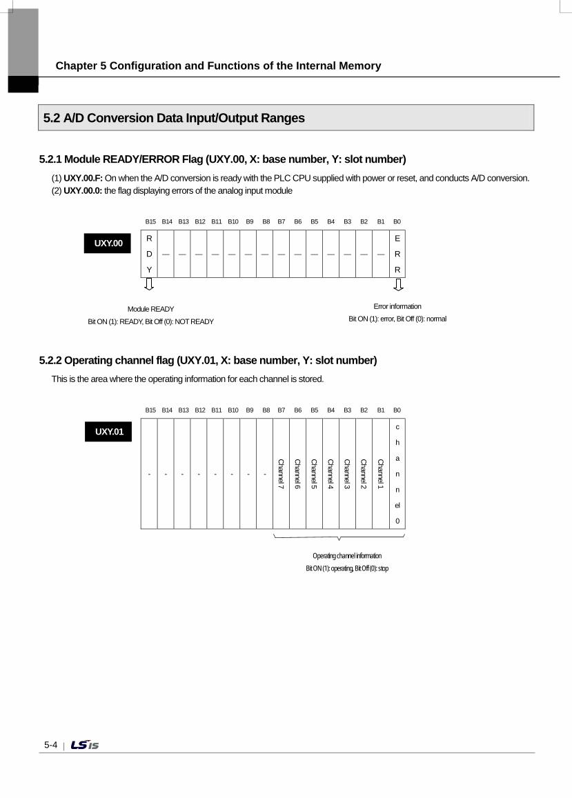
5.2.1 Module READY/ERROR Flag (UXY.00, X: base number, Y: slot number) (1) UXY.00.F: On when the A/D conversion is ready with the PLC CPU supplied with power or reset, and conducts A/D conversion.
(2) UXY.00.0: the flag displaying errors of the analog input module
5.2.2 Operating channel flag (UXY.01, X: base number, Y: slot number) This is the area where the operating information for each channel is stored.
B15 B14 B13 B12 B11 B10 B9 B8 B7 B6 B5 B4 B3 B2 B1 B0
R
D
Y
— — — — — — — — — — — — — —
E
R
R
B15 B14 B13 B12 B11 B10 B9 B8 B7 B6 B5 B4 B3 B2 B1 B0
- - - - - - - -
Channel 7
Channel 6
Channel 5
Channel 4
Channel 3
Channel 2
Channel 1
c
h
a
n
n
el
0
Operating channel information Bit ON (1): operating, Bit Off (0): stop
UXY.01
Error information
Bit ON (1): error, Bit Off (0): normal
UXY.00
Module READY
Bit ON (1): READY, Bit Off (0): NOT READY
Chapter 5 Configuration and Functions of the Internal Memory
5-5
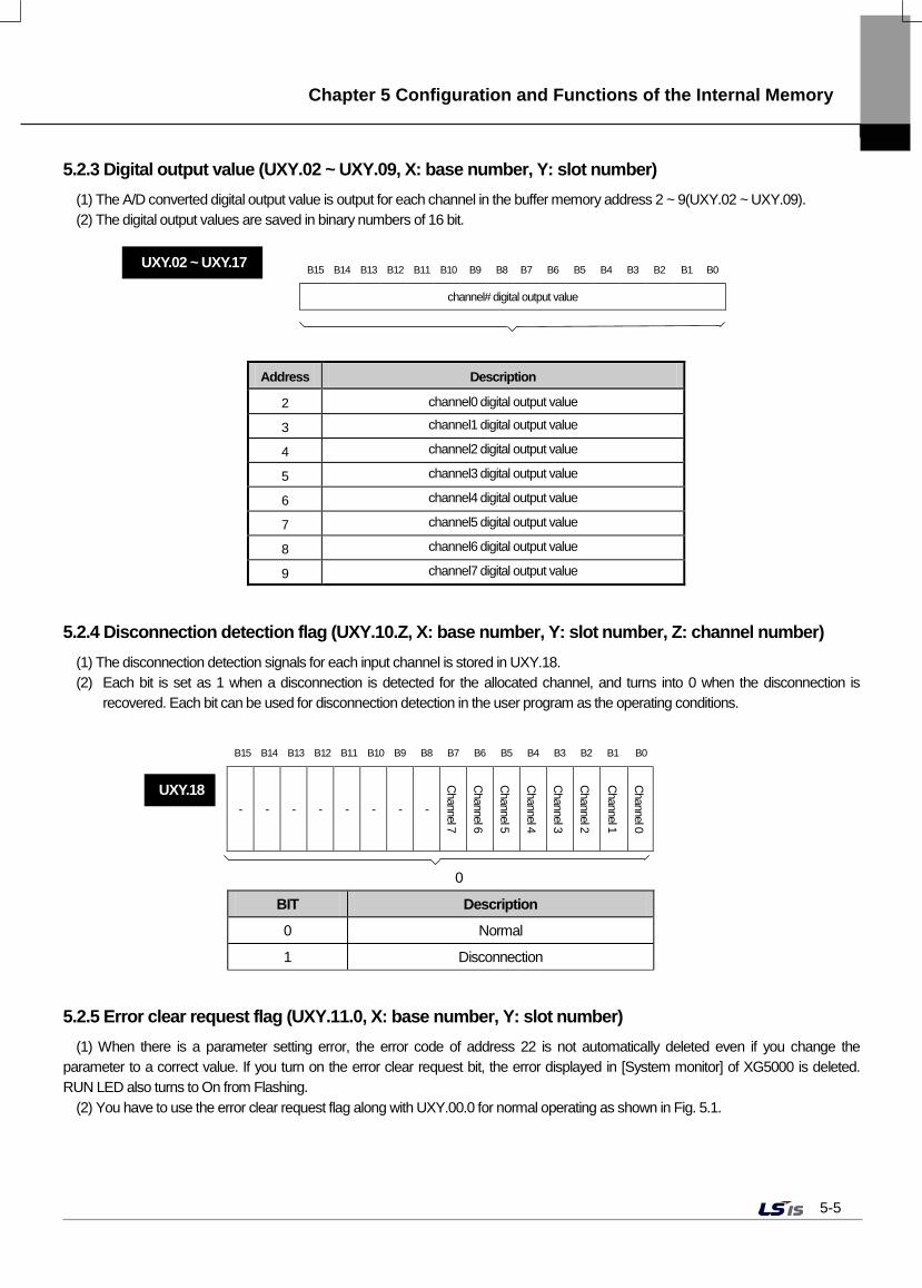
5.2.3 Digital output value (UXY.02 ~ UXY.09, X: base number, Y: slot number) (1) The A/D converted digital output value is output for each channel in the buffer memory address 2 ~ 9(UXY.02 ~ UXY.09). (2) The digital output values are saved in binary numbers of 16 bit.
B15 B14 B13 B12 B11 B10 B9 B8 B7 B6 B5 B4 B3 B2 B1 B0
channel# digital output value
Address Description
2 channel0 digital output value
3 channel1 digital output value
4 channel2 digital output value
5 channel3 digital output value
6 channel4 digital output value
7 channel5 digital output value
8 channel6 digital output value
9 channel7 digital output value
5.2.4 Disconnection detection flag (UXY.10.Z, X: base number, Y: slot number, Z: channel number) (1) The disconnection detection signals for each input channel is stored in UXY.18. (2) Each bit is set as 1 when a disconnection is detected for the allocated channel, and turns into 0 when the disconnection is
recovered. Each bit can be used for disconnection detection in the user program as the operating conditions.
0
BIT Description
0 Normal
1 Disconnection
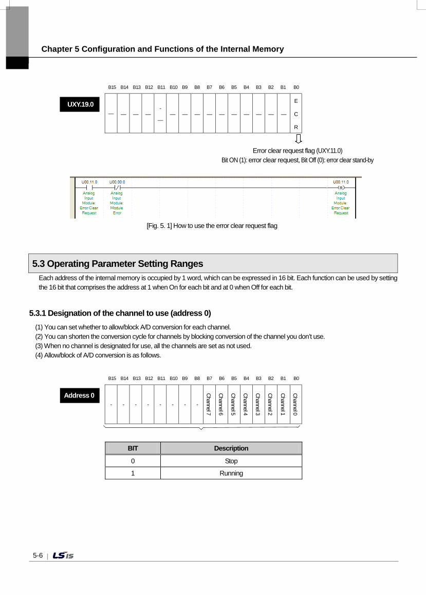
5.2.5 Error clear request flag (UXY.11.0, X: base number, Y: slot number) (1) When there is a parameter setting error, the error code of address 22 is not automatically deleted even if you change the
parameter to a correct value. If you turn on the error clear request bit, the error displayed in [System monitor] of XG5000 is deleted. RUN LED also turns to On from Flashing.
(2) You have to use the error clear request flag along with UXY.00.0 for normal operating as shown in Fig. 5.1.
B15 B14 B13 B12 B11 B10 B9 B8 B7 B6 B5 B4 B3 B2 B1 B0
- - - - - - - -
Channel 7
Channel 6
Channel 5
Channel 4
Channel 3
Channel 2
Channel 1
Channel 0
UXY.18
UXY.02 ~ UXY.17
Chapter 5 Configuration and Functions of the Internal Memory
5-6
[Fig. 5. 1] How to use the error clear request flag
5.3 Operating Parameter Setting Ranges Each address of the internal memory is occupied by 1 word, which can be expressed in 16 bit. Each function can be used by setting the 16 bit that comprises the address at 1 when On for each bit and at 0 when Off for each bit.
5.3.1 Designation of the channel to use (address 0) (1) You can set whether to allow/block A/D conversion for each channel. (2) You can shorten the conversion cycle for channels by blocking conversion of the channel you don’t use. (3) When no channel is designated for use, all the channels are set as not used. (4) Allow/block of A/D conversion is as follows.
BIT Description
0 Stop
1 Running
B15 B14 B13 B12 B11 B10 B9 B8 B7 B6 B5 B4 B3 B2 B1 B0
— — — — -
— — — — — — — — — — —
E
C
R
B15 B14 B13 B12 B11 B10 B9 B8 B7 B6 B5 B4 B3 B2 B1 B0
- - - - - - - -
Channel 7
Channel 6
Channel 5
Channel 4
Channel 3
Channel 2
Channel 1
Channel 0
UXY.19.0
Error clear request flag (UXY.11.0) Bit ON (1): error clear request, Bit Off (0): error clear stand-by
Address 0
Chapter 5 Configuration and Functions of the Internal Memory
5-7
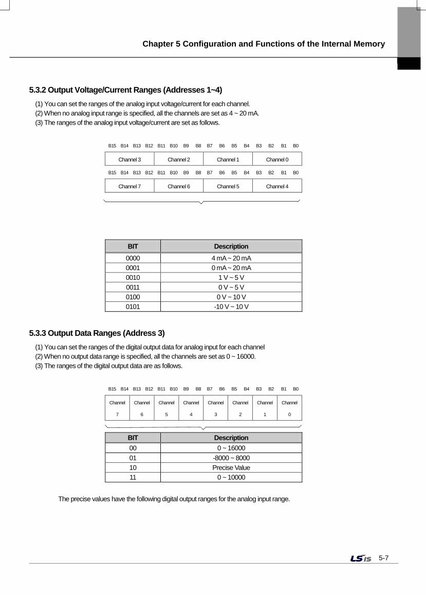
5.3.2 Output Voltage/Current Ranges (Addresses 1~4) (1) You can set the ranges of the analog input voltage/current for each channel. (2) When no analog input range is specified, all the channels are set as 4 ~ 20 mA. (3) The ranges of the analog input voltage/current are set as follows.
B15 B14 B13 B12 B11 B10 B9 B8 B7 B6 B5 B4 B3 B2 B1 B0
Channel 3 Channel 2 Channel 1 Channel 0
B15 B14 B13 B12 B11 B10 B9 B8 B7 B6 B5 B4 B3 B2 B1 B0
Channel 7 Channel 6 Channel 5 Channel 4
BIT Description 0000 4 mA ~ 20 mA 0001 0 mA ~ 20 mA 0010 1 V ~ 5 V 0011 0 V ~ 5 V 0100 0 V ~ 10 V 0101 -10 V ~ 10 V
5.3.3 Output Data Ranges (Address 3) (1) You can set the ranges of the digital output data for analog input for each channel (2) When no output data range is specified, all the channels are set as 0 ~ 16000. (3) The ranges of the digital output data are as follows.
B15 B14 B13 B12 B11 B10 B9 B8 B7 B6 B5 B4 B3 B2 B1 B0
Channel
7
Channel
6
Channel
5
Channel
4
Channel
3
Channel
2
Channel
1
Channel
0
BIT Description 00 0 ~ 16000 01 -8000 ~ 8000 10 Precise Value 11 0 ~ 10000
The precise values have the following digital output ranges for the analog input range.

Chapter 5 Configuration and Functions of the Internal Memory
5-8
(a) Current
Analog input Digital output
4 ~ 20 0 ~ 20
Precise Value 4000 ~ 20000 0 ~ 20000
(b) Voltage
Analog input Digital output
-10 ~ 10 V 0 ~ 10 V 0 ~ 5 V 1 ~ 5 V
Precise Value -10000 ~ 10000 0 ~ 10000 0 ~ 5000 1000 ~ 5000
5.3.4 Average Processing (Address 4) (1) This is the area where you designate the method of average processing. Average processing divides into ‘number average’ and
‘time average.’ (2) When you designate no average processing, all the channels conduct sampling processing. (3) The designation of average processing is as follows.
BIT Description 00 Sampling processing 01 Time average 10 Number average 11 Weighted average
5.3.5 Average Value (Addresses 5~12) (1) The setting ranges of the time/number/weighted averages are as follows.
(a) Time average: 16 ~ 16000(ms) (b) Number average: 2 ~ 64000(number of times) (c) Weighted average: 1 ~ 99(%)
(2) If you designate a value beyond the range, the address that displays the error code shows the following signals. (a) Beyond the time average range: error code #50 (b) Beyond the number average range: error code 60# (c) Beyond the weighted average range: error code 70$ In these cases, the initial value applies to the average processing. (# of the error code means the channel where the error occurred)
B15 B14 B13 B12 B11 B10 B9 B8 B7 B6 B5 B4 B3 B2 B1 B0
Channel
7
Channel
6
Channel
5
Channel
4
Channel
3
Channel
2
Channel
1
Channel
0
Address 7
Chapter 5 Configuration and Functions of the Internal Memory
5-9
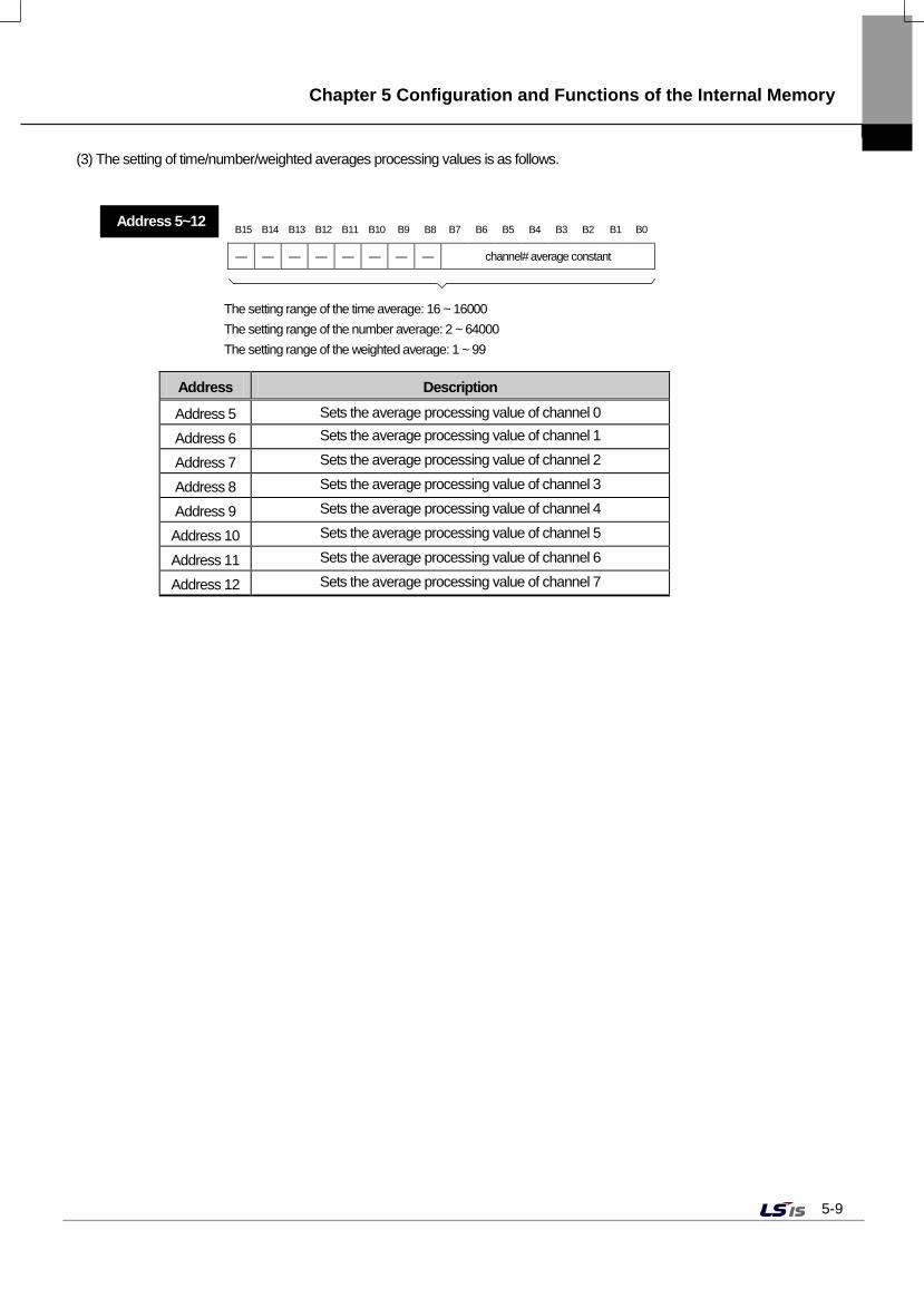
(3) The setting of time/number/weighted averages processing values is as follows.
B15 B14 B13 B12 B11 B10 B9 B8 B7 B6 B5 B4 B3 B2 B1 B0
— — — — — — — — channel# average constant
Address Description
Address 5 Sets the average processing value of channel 0
Address 6 Sets the average processing value of channel 1
Address 7 Sets the average processing value of channel 2
Address 8 Sets the average processing value of channel 3
Address 9 Sets the average processing value of channel 4
Address 10 Sets the average processing value of channel 5
Address 11 Sets the average processing value of channel 6
Address 12 Sets the average processing value of channel 7
Address 5~12
The setting range of the time average: 16 ~ 16000 The setting range of the number average: 2 ~ 64000 The setting range of the weighted average: 1 ~ 99
Chapter 5 Configuration and Functions of the Internal Memory
5-10
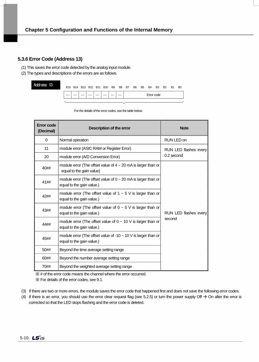
5.3.6 Error Code (Address 13) (1) This saves the error code detected by the analog input module. (2) The types and descriptions of the errors are as follows.
B15 B14 B13 B12 B11 B10 B9 B8 B7 B6 B5 B4 B3 B2 B1 B0
— — — — — — — — Error code
Error code (Decimal) Description of the error Note
0 Normal operation RUN LED on
11 module error (ASIC RAM or Register Error) RUN LED flashes every 0.2 second 20 module error (A/D Conversion Error)
40## module error (The offset value of 4 ~ 20 mA is larger than or equal to the gain value)
RUN LED flashes every second
41## module error (The offset value of 0 ~ 20 mA is larger than or equal to the gain value.)
42## module error (The offset value of 1 ~ 5 V is larger than or equal to the gain value.)
43## module error (The offset value of 0 ~ 5 V is larger than or equal to the gain value.)
44## module error (The offset value of 0 ~ 10 V is larger than or equal to the gain value.)
45## module error (The offset value of -10 ~ 10 V is larger than or equal to the gain value.)
50## Beyond the time average setting range
60## Beyond the number average setting range
70## Beyond the weighted average setting range
※ # of the error code means the channel where the error occurred. ※ For details of the error codes, see 9.1.
(3) If there are two or more errors, the module saves the error code that happened first and does not save the following error codes. (4) If there is an error, you should use the error clear request flag (see 5.2.5) or turn the power supply Off On after the error is
corrected so that the LED stops flashing and the error code is deleted.
Address 13
For the details of the error codes, see the table below.
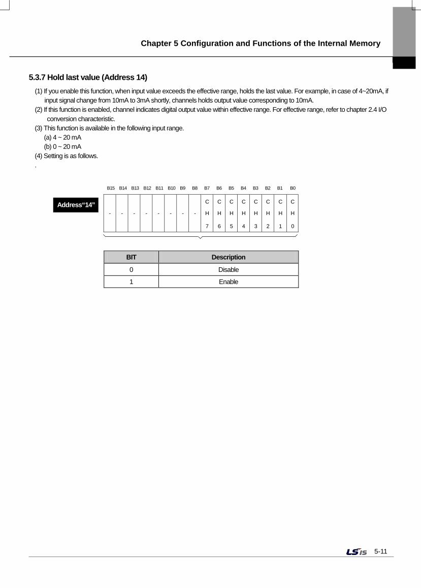
Chapter 5 Configuration and Functions of the Internal Memory
5-11
5.3.7 Hold last value (Address 14) (1) If you enable this function, when input value exceeds the effective range, holds the last value. For example, in case of 4~20mA, if
input signal change from 10mA to 3mA shortly, channels holds output value corresponding to 10mA. (2) If this function is enabled, channel indicates digital output value within effective range. For effective range, refer to chapter 2.4 I/O
conversion characteristic. (3) This function is available in the following input range.
(a) 4 ~ 20 mA (b) 0 ~ 20 mA
(4) Setting is as follows. .
BIT Description
0 Disable
1 Enable
B15 B14 B13 B12 B11 B10 B9 B8 B7 B6 B5 B4 B3 B2 B1 B0
- - - - - - - -
C
H
7
C
H
6
C
H
5
C
H
4
C
H
3
C
H
2
C
H
1
C
H
0
Address“14”
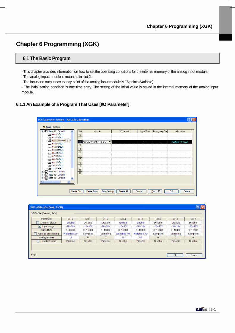
Chapter 6 Programming (XGK)
6-1
Chapter 6 Programming (XGK)
6.1 The Basic Program - This chapter provides information on how to set the operating conditions for the internal memory of the analog input module. - The analog input module is mounted in slot 2. - The input and output occupancy point of the analog input module is 16 points (variable). - The initial setting condition is one time entry. The setting of the initial value is saved in the internal memory of the analog input module.
6.1.1 An Example of a Program That Uses [I/O Parameter]
Chapter 6 Programming
6-2
6.1.2 An Example of a Program That Uses the PUT/GET Command
CH0 digital output
CH3 digital output
CH4 digital output
Reading error code
Module ready
Execution contact Device storing the data
to be transmitted
Device to store
transmitted data
CH operating signal
Internal memory address
Slot No.
Device to store
No. of data to read
Module ready
Execution contact
CH operating signal
Slot No.
Internal memory
address Setting data No. of word to write
Designate channel to use (channel 0, 3, 4).
Designate input range (-10~10V)
Designate input range (-10~10V)
Designate output data range (-192~16191)
Designate weighted average process (CH0, 3,
4)
Designate weighted average value (CH0)
Designate weighted average value (CH3)
Designate weighted average value (CH4)
CH0 digital output
CH03digital output
CH4 digital output
Chapter 6 Programming (XGK)
6-3
6.2 Application Program (XGK)
6.2.1 The Program Distinguishing A/D Conversion Values (I/O slot fixed point allocation: 64 points) (1) System configuration
(2) Initial setting
No. Item Initial setting Internal memory address
Values to write in internal memory
1 Channel in use channel 0, channel 2, channel 4 0 ‘h0015’ or ‘21’
2 Input range -10 ~ 10 V 1, 2 ‘hFFFF’ or ‘65535’
3 Output data range 0 ~ 16000 3 ‘h0000’ or ‘0’
4 Average processing channel 2: number average
channel 4: time average 4 ‘h0120’ or ‘288’
5 Average
channel 2 number average:
100(times) 7 ‘h0064’ or ‘100’
channel 4 time average: 200(ms) 9 ‘h00C8’ or ‘200’
(3) Program description
(a) When the digital value of channel 0 is smaller than 12000, contact point 0 (P00080) of the relay output module mounted in slot 2 is On.
(b) When the digital value of channel 2 is greater than 13600, contact point 2 (P00082) of the relay output module mounted in slot 2 is On.
(c) When the digital value of channel 4 is greater than or equal to 12000 and smaller than or equal to 13600, contact point 4 (P00086) of the relay output module mounted in slot 2 is On.
(d) When the digital value of channel 4 is 12800, contact point 5 (P00085) of the relay output module mounted in slot 2 is On.
XGP-
ACF2
XGK-
CPUS
XGI-
D24A
XGF-
AD16A
XGQ-
RY2A
Chapter 6 Programming
6-4
(4) Program
(a) An example of the program that uses [I/O parameter] setting
Module ready Execution contact
CH operating signal
Slot no.
Internal memoryaddress
Storage device
No. of data to read
Reading error code
Chapter 6 Programming (XGK)
6-5
(b) An example of the program that uses PUT/GET command
Module ready
Program run wait
Slot No.
Internal memoryaddress
Setting dataNo. of word to write
Storage device No. of word to read
Designate input rage (-10~10V)
Designate channel to use (channel 0, 3, 4).
Designate input rage (-10~10V)
Designate output data range (-192~16191)
Designate average process
(CH2: count average, Ch4: time average)
Designate average value (CH4:200)
Designate average value (CH0:100)
P00084 ON if the A/D conversion value in channel 4 is between 12000 and 13600
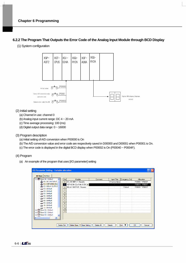
Chapter 6 Programming
6-6
6.2.2 The Program That Outputs the Error Code of the Analog Input Module through BCD Display (1) System configuration
(2) Initial setting
(a) Channel in use: channel 0 (b) Analog input current range: DC 4 ~ 20 mA (c) Time average processing: 100 (ms) (d) Digital output data range: 0 ~ 16000
(3) Program description (a) Initial setting of A/D conversion when P00000 is On (b) The A/D conversion value and error code are respectively saved in D00000 and D00001 when P00001 is On. (c) The error code is displayed in the digital BCD display when P00002 is On (P00040 ~ P0004F).
(4) Program
(a) An example of the program that uses [I/O parameter] setting
XGP-
ACF2
XGT-
CPUS
XGI-
D24A
XGQ-
RY2A
XGF-
AD8A
Digital BCD display (displays
errors)
XGQ-
RY2A
Initial value
Outputs error code thru BCD
P0000
P000
P0002
Saves A/D conversion value
and error code
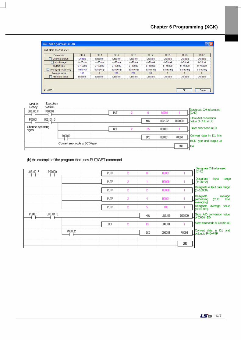
Chapter 6 Programming (XGK)
6-7
(b) An example of the program that uses PUT/GET command
Module Ready
Execution contact
Channel operating signal
Convert error code to BCD type
Designate CH to be used(CH0)
Store A/D conversionvalue of CH0 in D0
Store error code in D1
Convert data in D1 into
BCD type and output at
P4
Designate CH to be used(CH0)
Designate input range (4~20mA)
Designate output data range(0~16000)
Designate averageprocessing (CH0: timeaveraging) Designate average value(CH0: 100)
Store A/D conversion valueof CH0 in D0
Store error code of CH0 in D1
Convert data in D1 andoutput to P40~P4F
Chapter 7 Configuration and Functions of Global Variables (XGI/XGR)
7-1
Chapter 7 Configuration and Functions of Global Variables (for XGI/XGR)
7.1 Global Variables (Data Areas)
7.1.1 Configuration of A/D Conversion Data Input and Output Area Table 7.1 shows the A/D conversion data input and output Area
[Table 7. 1] A/D conversion data input and output ranges
Global variables Memory allocation Description R/W
_xxyy_ERR _xxyy_RDY
%UXxx.yy.0 %UXxx.yy.15
Module error flag Module READY flag
Read
_xxyy_CH0_ACT _xxyy_CH1_ACT _xxyy_CH2_ACT _xxyy_CH3_ACT _xxyy_CH4_ACT _xxyy_CH5_ACT _xxyy_CH6_ACT _xxyy_CH7_ACT
%UXxx.yy.16 %UXxx.yy.17 %UXxx.yy.18 %UXxx.yy.19 %UXxx.yy.20 %UXxx.yy.21 %UXxx.yy.22 %UXxx.yy.23
channel 0 operating flag channel 1 operating flag channel 2 operating flag channel 3 operating flag channel 4 operating flag channel 5 operating flag channel 6 operating flag channel 7 operating flag
Read
_xxyy_CH0_DATA _xxyy_CH1_DATA _xxyy_CH2_DATA _xxyy_CH3_DATA _xxyy_CH4_DATA _xxyy_CH5_DATA _xxyy_CH6_DATA _xxyy_CH7_DATA
%UWxx.yy.2 %UWxx.yy.3 %UWxx.yy.4 %UWxx.yy.5 %UWxx.yy.6 %UWxx.yy.7 %UWxx.yy.8 %UWxx.yy.9
channel 0 digital output value (conversion value) channel 1 digital output value (conversion value) channel 2 digital output value (conversion value) channel 3 digital output value (conversion value) channel 4 digital output value (conversion value) channel 5 digital output value (conversion value) channel 6 digital output value (conversion value) channel 7 digital output value (conversion value)
Read
_xxyy_CH0_IDD _xxyy_CH1_IDD _xxyy_CH2_IDD _xxyy_CH3_IDD _xxyy_CH4_IDD _xxyy_CH5_IDD _xxyy_CH6_IDD _xxyy_CH7_IDD
%UXxx.yy.160 %UXxx.yy.161 %UXxx.yy.162 %UXxx.yy.163 %UXxx.yy.164 %UXxx.yy.165 %UXxx.yy.166 %UXxx.yy.167
channel 0 input disconnection detection flag channel 1 input disconnection detection flag channel 2 input disconnection detection flag channel 3 input disconnection detection flag channel 4 input disconnection detection flag channel 5 input disconnection detection flag channel 6 input disconnection detection flag channel 7 input disconnection detection flag
Read
_xxyy_ERR_CLR %UXxx.yy.176 Error clear request flag Write _xxyy_CH0_HOOR _xxyy_CH1_HOOR _xxyy_CH2_HOOR _xxyy_CH3_HOOR _xxyy_CH4_HOOR _xxyy_CH5_HOOR _xxyy_CH6_HOOR _xxyy_CH7_HOOR
%UXxx.yy.320 %UXxx.yy.321 %UXxx.yy.322 %UXxx.yy.323 %UXxx.yy.324 %UXxx.yy.325 %UXxx.yy.326 %UXxx.yy.327
CH0 alarm upper limit CH1 alarm upper limit CH2 alarm upper limit CH3 alarm upper limit CH4 alarm upper limit CH5 alarm upper limit CH6 alarm upper limit CH7 alarm upper limit
Read
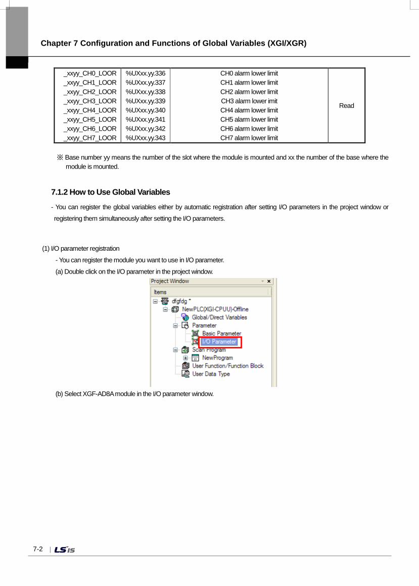
Chapter 7 Configuration and Functions of Global Variables (XGI/XGR)
7-2
_xxyy_CH0_LOOR _xxyy_CH1_LOOR _xxyy_CH2_LOOR _xxyy_CH3_LOOR _xxyy_CH4_LOOR _xxyy_CH5_LOOR _xxyy_CH6_LOOR _xxyy_CH7_LOOR
%UXxx.yy.336 %UXxx.yy.337 %UXxx.yy.338 %UXxx.yy.339 %UXxx.yy.340 %UXxx.yy.341 %UXxx.yy.342 %UXxx.yy.343
CH0 alarm lower limit CH1 alarm lower limit CH2 alarm lower limit CH3 alarm lower imit CH4 alarm lower limit CH5 alarm lower limit CH6 alarm lower limit CH7 alarm lower limit
Read
※ Base number yy means the number of the slot where the module is mounted and xx the number of the base where the
module is mounted.
7.1.2 How to Use Global Variables
- You can register the global variables either by automatic registration after setting I/O parameters in the project window or
registering them simultaneously after setting the I/O parameters.
(1) I/O parameter registration
- You can register the module you want to use in I/O parameter.
(a) Double click on the I/O parameter in the project window.
(b) Select XGF-AD8A module in the I/O parameter window.
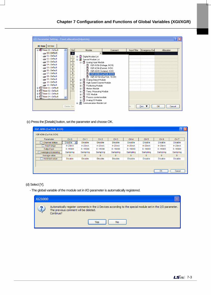
Chapter 7 Configuration and Functions of Global Variables (XGI/XGR)
7-3
(c) Press the [Details] button, set the parameter and choose OK.
(d) Select [Y].
- The global variable of the module set in I/O parameter is automatically registered.
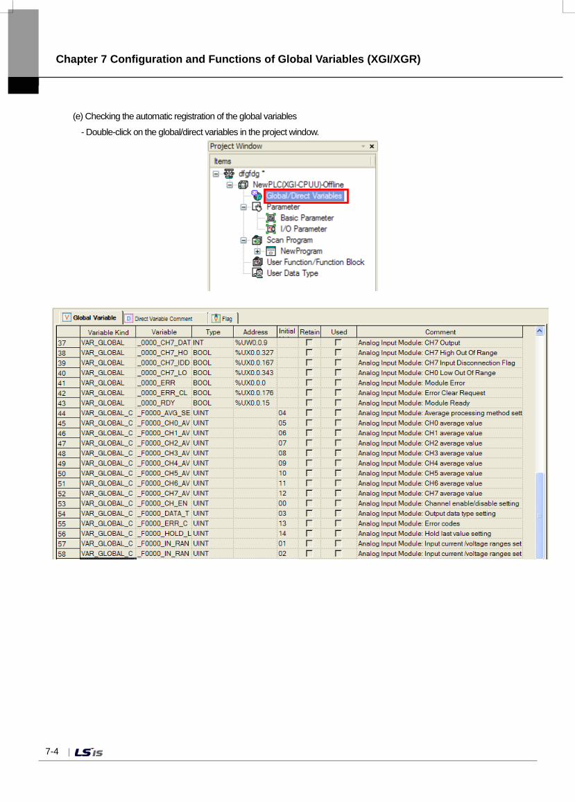
Chapter 7 Configuration and Functions of Global Variables (XGI/XGR)
7-4
(e) Checking the automatic registration of the global variables
- Double-click on the global/direct variables in the project window.
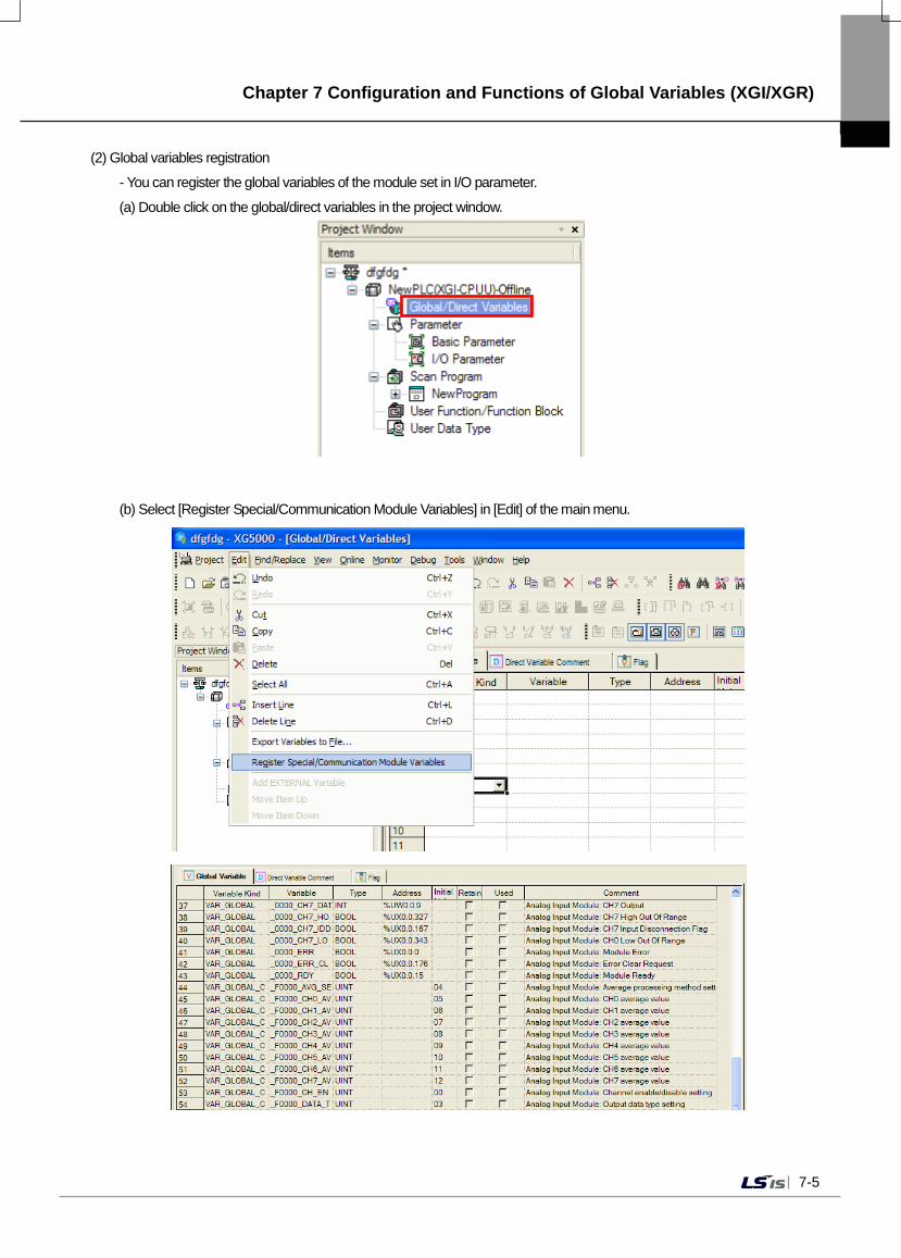
Chapter 7 Configuration and Functions of Global Variables (XGI/XGR)
7-5
(2) Global variables registration
- You can register the global variables of the module set in I/O parameter.
(a) Double click on the global/direct variables in the project window.
(b) Select [Register Special/Communication Module Variables] in [Edit] of the main menu.
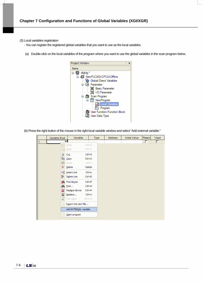
Chapter 7 Configuration and Functions of Global Variables (XGI/XGR)
7-6
(3) Local variables registration
- You can register the registered global variables that you want to use as the local variables.
(a) Double-click on the local variables of the program where you want to use the global variables in the scan program below.
(b) Press the right button of the mouse in the right local variable window and select “Add external variable.”
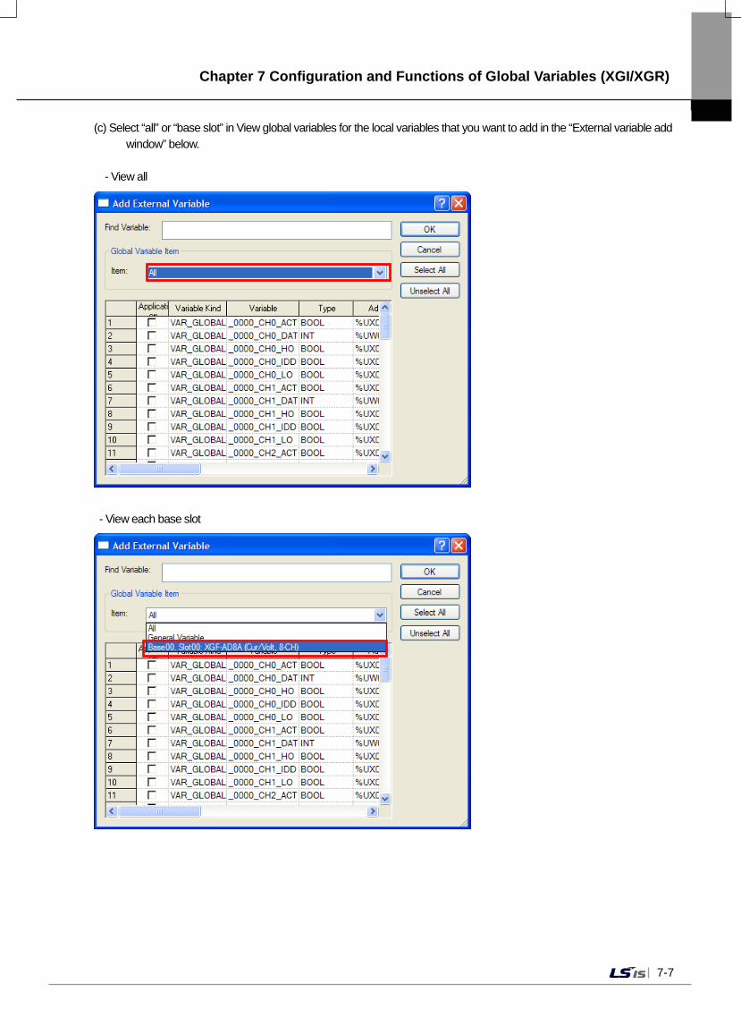
Chapter 7 Configuration and Functions of Global Variables (XGI/XGR)
7-7
(c) Select “all” or “base slot” in View global variables for the local variables that you want to add in the “External variable add window” below.
- View all
- View each base slot
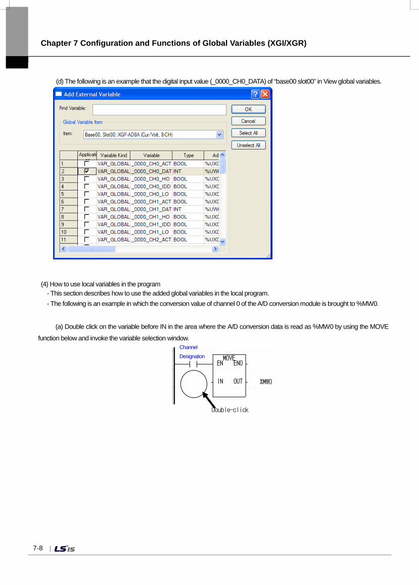
Chapter 7 Configuration and Functions of Global Variables (XGI/XGR)
7-8
(d) The following is an example that the digital input value (_0000_CH0_DATA) of “base00 slot00” in View global variables.
(4) How to use local variables in the program - This section describes how to use the added global variables in the local program. - The following is an example in which the conversion value of channel 0 of the A/D conversion module is brought to %MW0.
(a) Double click on the variable before IN in the area where the A/D conversion data is read as %MW0 by using the MOVE
function below and invoke the variable selection window.
Double-click
Channel
Designation
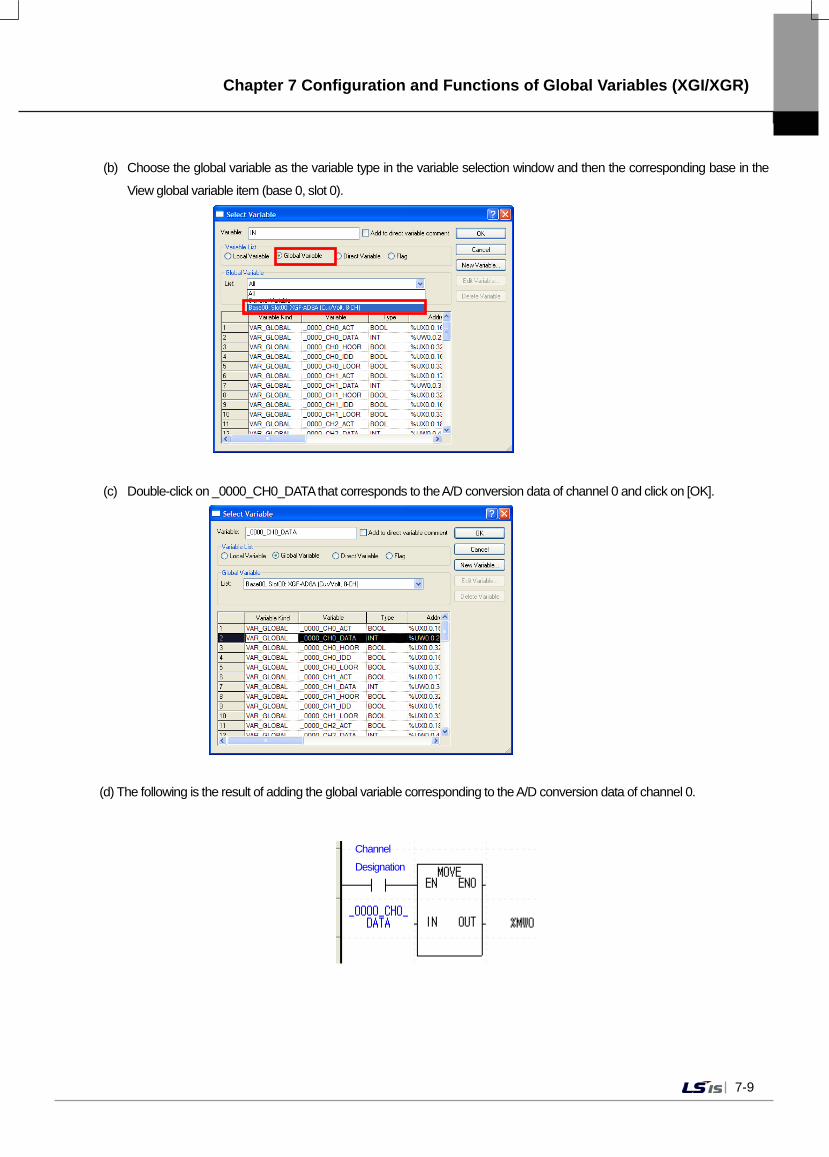
Chapter 7 Configuration and Functions of Global Variables (XGI/XGR)
7-9
(b) Choose the global variable as the variable type in the variable selection window and then the corresponding base in the
View global variable item (base 0, slot 0).
(c) Double-click on _0000_CH0_DATA that corresponds to the A/D conversion data of channel 0 and click on [OK].
(d) The following is the result of adding the global variable corresponding to the A/D conversion data of channel 0.
Channel
Designation
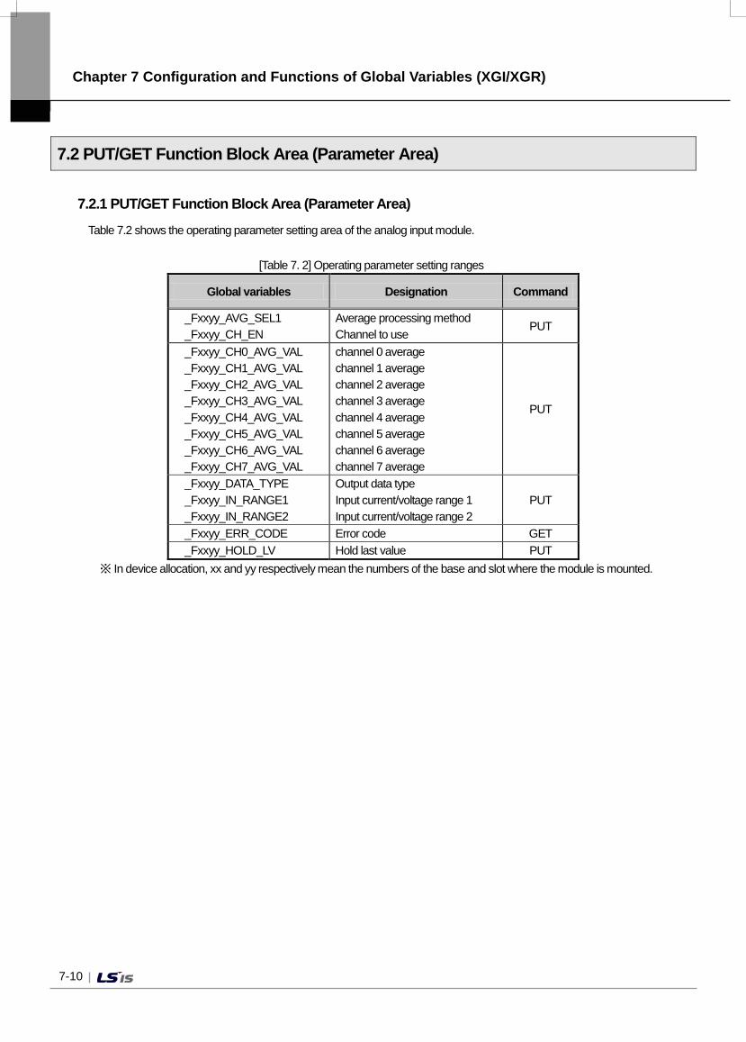
Chapter 7 Configuration and Functions of Global Variables (XGI/XGR)
7-10
7.2 PUT/GET Function Block Area (Parameter Area)
7.2.1 PUT/GET Function Block Area (Parameter Area)
Table 7.2 shows the operating parameter setting area of the analog input module.
[Table 7. 2] Operating parameter setting ranges
Global variables Designation Command
_Fxxyy_AVG_SEL1 _Fxxyy_CH_EN
Average processing method Channel to use
PUT
_Fxxyy_CH0_AVG_VAL _Fxxyy_CH1_AVG_VAL _Fxxyy_CH2_AVG_VAL _Fxxyy_CH3_AVG_VAL _Fxxyy_CH4_AVG_VAL _Fxxyy_CH5_AVG_VAL _Fxxyy_CH6_AVG_VAL _Fxxyy_CH7_AVG_VAL
channel 0 average channel 1 average channel 2 average channel 3 average channel 4 average channel 5 average channel 6 average channel 7 average
PUT
_Fxxyy_DATA_TYPE _Fxxyy_IN_RANGE1 _Fxxyy_IN_RANGE2
Output data type Input current/voltage range 1 Input current/voltage range 2
PUT
_Fxxyy_ERR_CODE Error code GET _Fxxyy_HOLD_LV Hold last value PUT
※ In device allocation, xx and yy respectively mean the numbers of the base and slot where the module is mounted.
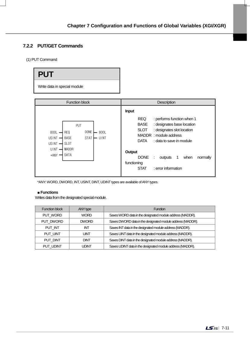
Chapter 7 Configuration and Functions of Global Variables (XGI/XGR)
7-11
7.2.2 PUT/GET Commands (1) PUT Command
PUT
Write data in special module
Function block Description
UINT
PUT
DONE
BASE
SLOT
MADDR
STAT
BOOL
USINT
UINT
USINT
*ANY DATA
REQBOOL
Input
REQ : performs function when 1 BASE : designates base location SLOT : designates slot location MADDR : module address DATA : data to save in module Output
DONE : outputs 1 when normally functioning STAT : error information
*ANY: WORD, DWORD, INT, USINT, DINT, UDINT types are available of ANY types.
Functions Writes data from the designated special module.
Function block ANY type Function
PUT_WORD WORD Saves WORD data in the designated module address (MADDR).
PUT_DWORD DWORD Saves DWORD data in the designated module address (MADDR).
PUT_INT INT Saves INT data in the designated module address (MADDR).
PUT_UINT UINT Saves UINT data in the designated module address (MADDR).
PUT_DINT DINT Saves DINT data in the designated module address (MADDR).
PUT_UDINT UDINT Saves UDINT data in the designated module address (MADDR).
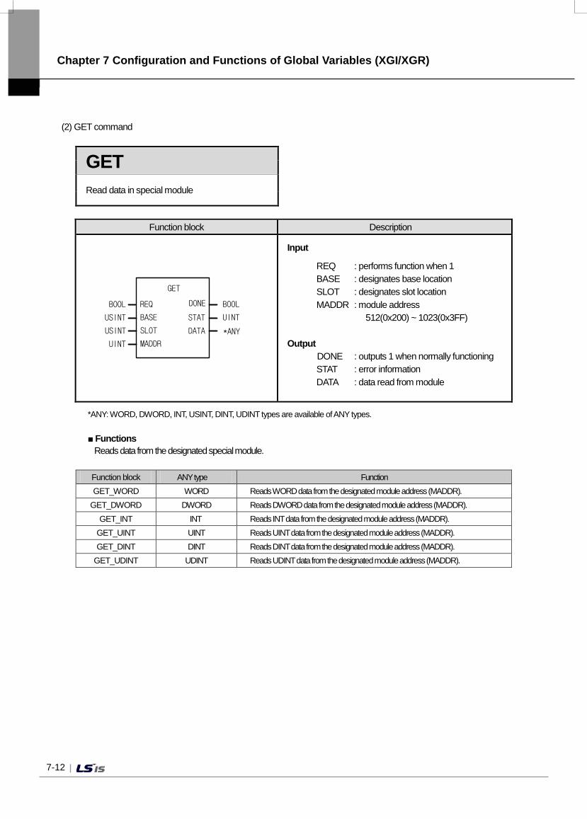
Chapter 7 Configuration and Functions of Global Variables (XGI/XGR)
7-12
(2) GET command
GET
Read data in special module
Function block Description
UINT
GET
DONE
BASE
SLOT
MADDR
STAT
BOOL
USINT
UINT
USINT *ANYDATA
REQBOOL
Input
REQ : performs function when 1 BASE : designates base location SLOT : designates slot location MADDR : module address
512(0x200) ~ 1023(0x3FF) Output
DONE : outputs 1 when normally functioning STAT : error information DATA : data read from module
*ANY: WORD, DWORD, INT, USINT, DINT, UDINT types are available of ANY types.
Functions Reads data from the designated special module.
Function block ANY type Function GET_WORD WORD Reads WORD data from the designated module address (MADDR).
GET_DWORD DWORD Reads DWORD data from the designated module address (MADDR). GET_INT INT Reads INT data from the designated module address (MADDR).
GET_UINT UINT Reads UINT data from the designated module address (MADDR). GET_DINT DINT Reads DINT data from the designated module address (MADDR).
GET_UDINT UDINT Reads UDINT data from the designated module address (MADDR).
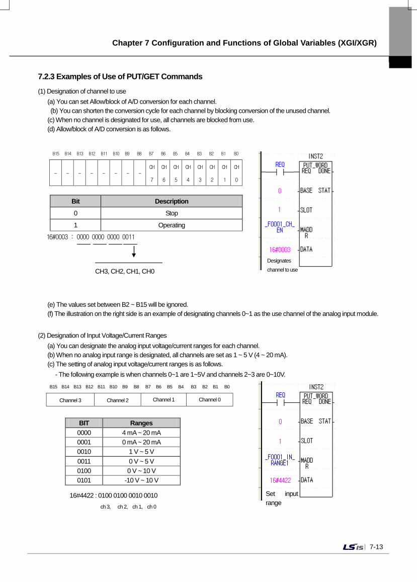
Chapter 7 Configuration and Functions of Global Variables (XGI/XGR)
7-13
7.2.3 Examples of Use of PUT/GET Commands
(1) Designation of channel to use (a) You can set Allow/block of A/D conversion for each channel. (b) You can shorten the conversion cycle for each channel by blocking conversion of the unused channel. (c) When no channel is designated for use, all channels are blocked from use. (d) Allow/block of A/D conversion is as follows.
B15 B14 B13 B12 B11 B10 B9 B8 B7 B6 B5 B4 B3 B2 B1 B0
- - - - - - - - CH
7
CH
6
CH
5
CH
4
CH
3
CH
2
CH
1
CH
0
16#0003 : 0000 0000 0000 0011
CH3, CH2, CH1, CH0
Bit Description
0 Stop
1 Operating
(e) The values set between B2 ~ B15 will be ignored. (f) The illustration on the right side is an example of designating channels 0~1 as the use channel of the analog input module.
(2) Designation of Input Voltage/Current Ranges (a) You can designate the analog input voltage/current ranges for each channel. (b) When no analog input range is designated, all channels are set as 1 ~ 5 V (4 ~ 20 mA). (c) The setting of analog input voltage/current ranges is as follows.
- The following example is when channels 0~1 are 1~5V and channels 2~3 are 0~10V.
B15 B14 B13 B12 B11 B10 B9 B8 B7 B6 B5 B4 B3 B2 B1 B0
Channel 3 Channel 2 Channel 1 Channel 0
BIT Ranges
0000 4 mA ~ 20 mA 0001 0 mA ~ 20 mA 0010 1 V ~ 5 V 0011 0 V ~ 5 V 0100 0 V ~ 10 V 0101 -10 V ~ 10 V
Designates
channel to use
Set input range
16#4422 : 0100 0100 0010 0010 ch 3, ch 2, ch 1, ch 0
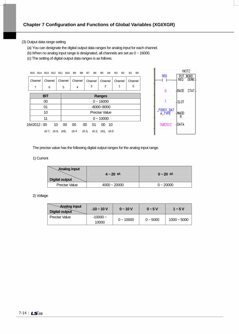
Chapter 7 Configuration and Functions of Global Variables (XGI/XGR)
7-14
(3) Output data range setting (a) You can designate the digital output data ranges for analog input for each channel. (b) When no analog input range is designated, all channels are set as 0 ~ 16000. (c) The setting of digital output data ranges is as follows.
B15 B14 B13 B12 B11 B10 B9 B8 B7 B6 B5 B4 B3 B2 B1 B0
Channel
7
Channel
6
Channel
5
Channel
4
Channel
3 Channel
2 Channel
1 Channel
0
16#2012 : 00 10 00 00 00 01 00 10 ch 7, ch 6, ch5, ch 4 ch 3, ch 2, ch1, ch 0
BIT Ranges 00 0 ~ 16000 01 -8000~8000 10 Precise Value 11 0 ~ 10000
The precise value has the following digital output ranges for the analog input range.
1) Current
Analog input
Digital output
4 ~ 20 0 ~ 20
Precise Value 4000 ~ 20000 0 ~ 20000
2) Voltage
Analog input Digital output -10 ~ 10 V 0 ~ 10 V 0 ~ 5 V 1 ~ 5 V
Precise Value -10000 ~ 10000
0 ~ 10000 0 ~ 5000 1000 ~ 5000
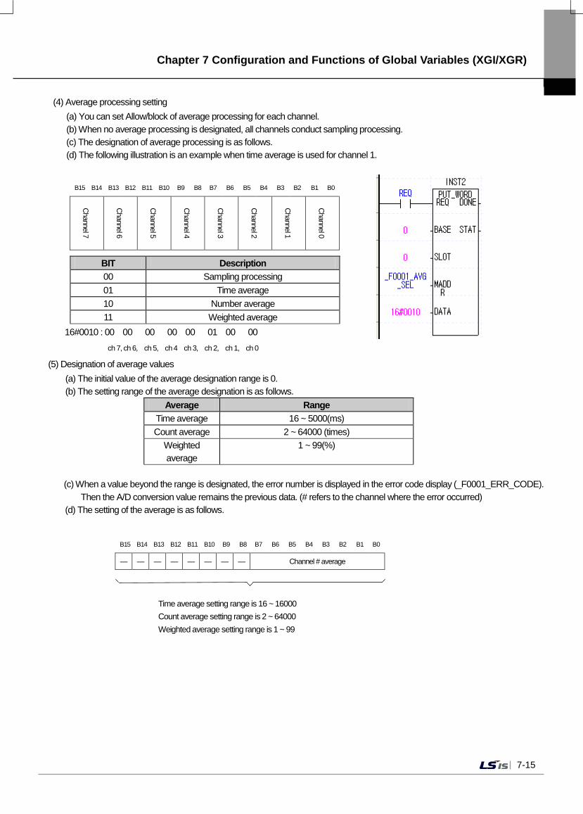
Chapter 7 Configuration and Functions of Global Variables (XGI/XGR)
7-15
(4) Average processing setting (a) You can set Allow/block of average processing for each channel. (b) When no average processing is designated, all channels conduct sampling processing. (c) The designation of average processing is as follows. (d) The following illustration is an example when time average is used for channel 1.
B15 B14 B13 B12 B11 B10 B9 B8 B7 B6 B5 B4 B3 B2 B1 B0
Channel 7
Channel 6
Channel 5
Channel 4
Channel 3
Channel 2
Channel 1
Channel 0
16#0010 : 00 00 00 00 00 01 00 00 ch 7, ch 6, ch 5, ch 4 ch 3, ch 2, ch 1, ch 0
BIT Description 00 Sampling processing 01 Time average 10 Number average 11 Weighted average
(5) Designation of average values (a) The initial value of the average designation range is 0. (b) The setting range of the average designation is as follows.
Average Range Time average 16 ~ 5000(ms) Count average 2 ~ 64000 (times)
Weighted average
1 ~ 99(%)
(c) When a value beyond the range is designated, the error number is displayed in the error code display (_F0001_ERR_CODE).
Then the A/D conversion value remains the previous data. (# refers to the channel where the error occurred) (d) The setting of the average is as follows.
B15 B14 B13 B12 B11 B10 B9 B8 B7 B6 B5 B4 B3 B2 B1 B0
— — — — — — — — Channel # average
Time average setting range is 16 ~ 16000 Count average setting range is 2 ~ 64000 Weighted average setting range is 1 ~ 99
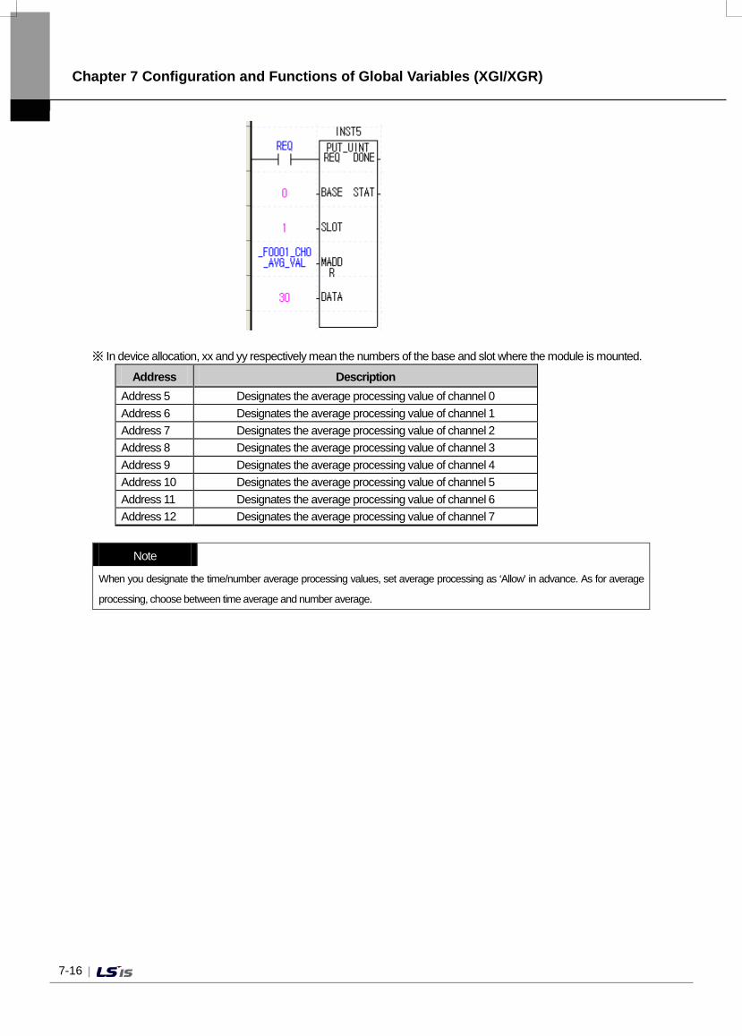
Chapter 7 Configuration and Functions of Global Variables (XGI/XGR)
7-16
※ In device allocation, xx and yy respectively mean the numbers of the base and slot where the module is mounted.
Address Description Address 5 Designates the average processing value of channel 0 Address 6 Designates the average processing value of channel 1 Address 7 Designates the average processing value of channel 2 Address 8 Designates the average processing value of channel 3 Address 9 Designates the average processing value of channel 4 Address 10 Designates the average processing value of channel 5 Address 11 Designates the average processing value of channel 6 Address 12 Designates the average processing value of channel 7
Note
When you designate the time/number average processing values, set average processing as ‘Allow’ in advance. As for average
processing, choose between time average and number average.
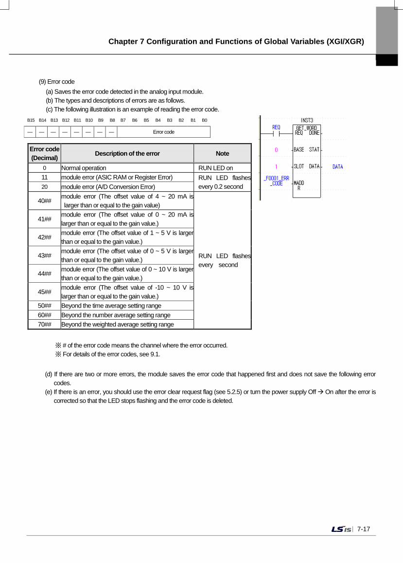
Chapter 7 Configuration and Functions of Global Variables (XGI/XGR)
7-17
(9) Error code (a) Saves the error code detected in the analog input module. (b) The types and descriptions of errors are as follows. (c) The following illustration is an example of reading the error code.
B15 B14 B13 B12 B11 B10 B9 B8 B7 B6 B5 B4 B3 B2 B1 B0
— — — — — — — — Error code
Error code (Decimal) Description of the error Note
0 Normal operation RUN LED on 11 module error (ASIC RAM or Register Error) RUN LED flashes
every 0.2 second 20 module error (A/D Conversion Error)
40## module error (The offset value of 4 ~ 20 mA is larger than or equal to the gain value)
RUN LED flashes every second
41## module error (The offset value of 0 ~ 20 mA is larger than or equal to the gain value.)
42## module error (The offset value of 1 ~ 5 V is larger than or equal to the gain value.)
43## module error (The offset value of 0 ~ 5 V is larger than or equal to the gain value.)
44## module error (The offset value of 0 ~ 10 V is larger than or equal to the gain value.)
45## module error (The offset value of -10 ~ 10 V is larger than or equal to the gain value.)
50## Beyond the time average setting range 60## Beyond the number average setting range 70## Beyond the weighted average setting range
※ # of the error code means the channel where the error occurred. ※ For details of the error codes, see 9.1.
(d) If there are two or more errors, the module saves the error code that happened first and does not save the following error
codes. (e) If there is an error, you should use the error clear request flag (see 5.2.5) or turn the power supply Off On after the error is
corrected so that the LED stops flashing and the error code is deleted.
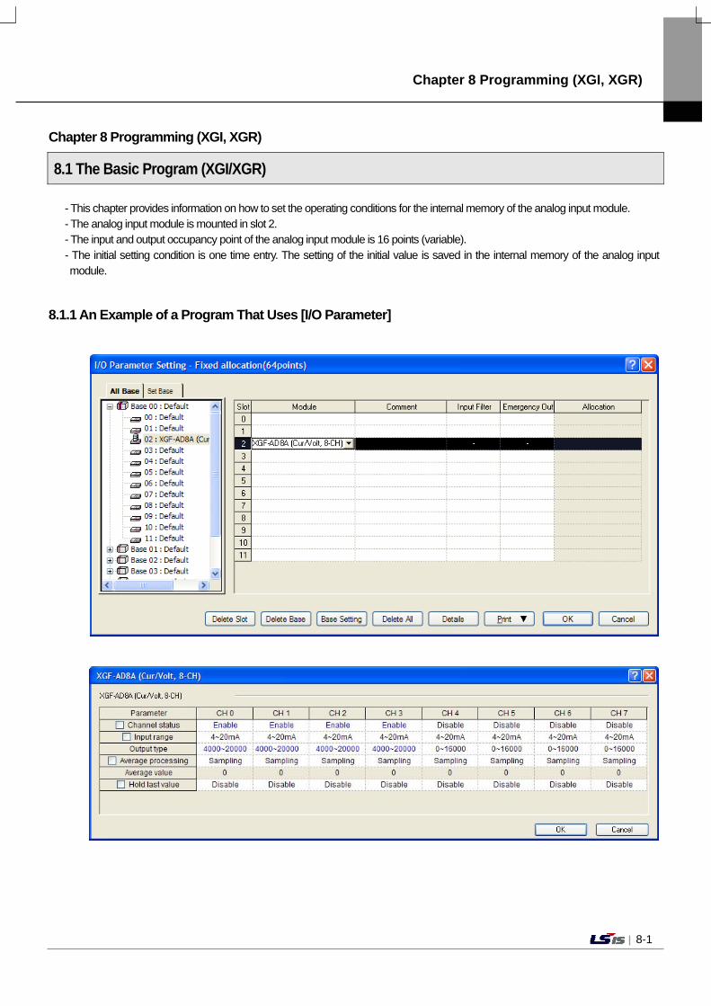
Chapter 8 Programming (XGI, XGR)
8-1
Chapter 8 Programming (XGI, XGR)
8.1 The Basic Program (XGI/XGR) - This chapter provides information on how to set the operating conditions for the internal memory of the analog input module. - The analog input module is mounted in slot 2. - The input and output occupancy point of the analog input module is 16 points (variable). - The initial setting condition is one time entry. The setting of the initial value is saved in the internal memory of the analog input module.
8.1.1 An Example of a Program That Uses [I/O Parameter]
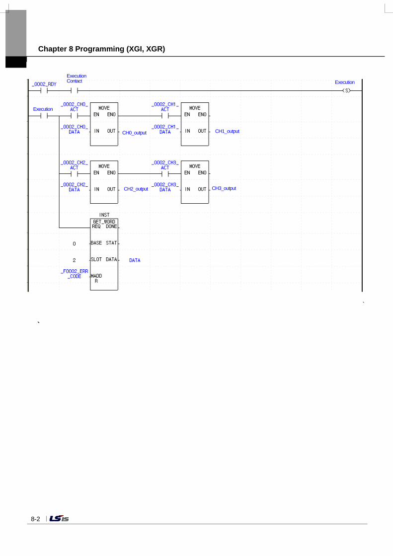
Chapter 8 Programming (XGI, XGR)
8-2
`
Execution Contact Execution
Execution
CH0_output
CH2_output
CH1_output
CH3_output
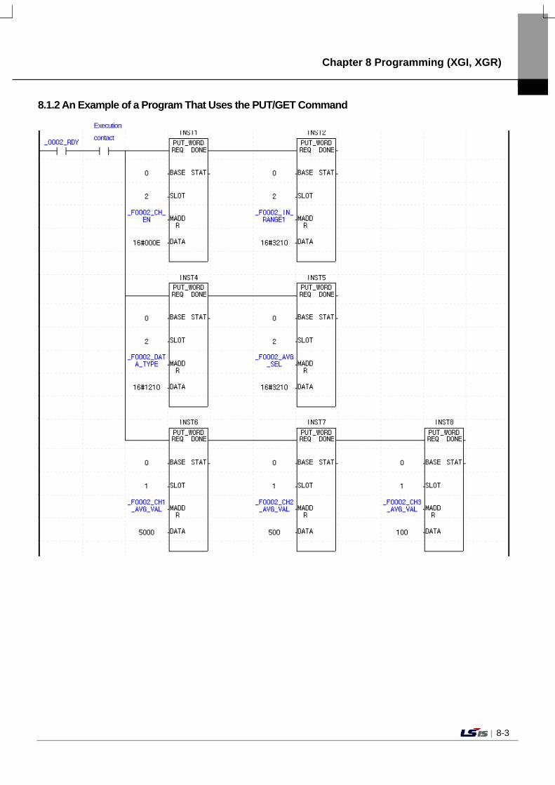
Chapter 8 Programming (XGI, XGR)
8-3
8.1.2 An Example of a Program That Uses the PUT/GET Command
Execution
contact
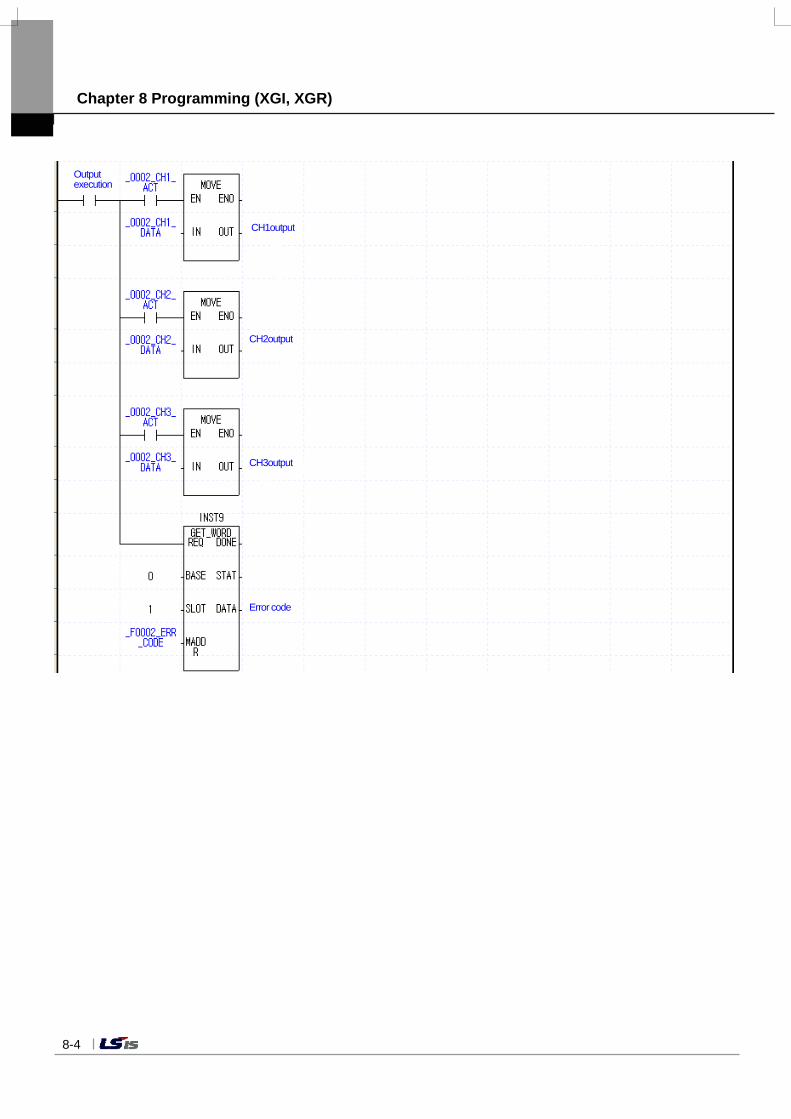
Chapter 8 Programming (XGI, XGR)
8-4
Output execution
CH1output
CH2output
CH3output
Error code
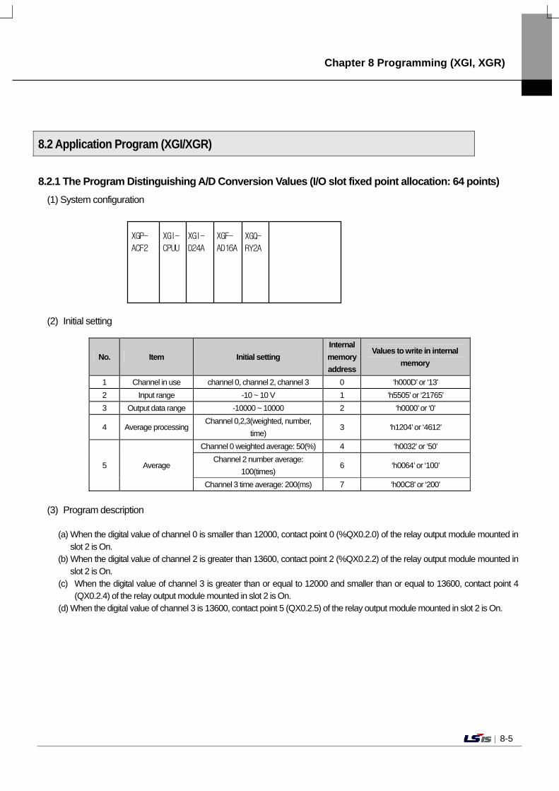
Chapter 8 Programming (XGI, XGR)
8-5
8.2 Application Program (XGI/XGR)
8.2.1 The Program Distinguishing A/D Conversion Values (I/O slot fixed point allocation: 64 points) (1) System configuration
(2) Initial setting
No. Item Initial setting Internal memory address
Values to write in internal memory
1 Channel in use channel 0, channel 2, channel 3 0 ‘h000D’ or ‘13’
2 Input range -10 ~ 10 V 1 ‘h5505’ or ‘21765’
3 Output data range -10000 ~ 10000 2 ‘h0000’ or ‘0’
4 Average processing Channel 0,2,3(weighted, number,
time) 3 ‘h1204’ or ‘4612’
5 Average
Channel 0 weighted average: 50(%) 4 ‘h0032’ or ‘50’
Channel 2 number average:
100(times) 6 ‘h0064’ or ‘100’
Channel 3 time average: 200(ms) 7 ‘h00C8’ or ‘200’
(3) Program description
(a) When the digital value of channel 0 is smaller than 12000, contact point 0 (%QX0.2.0) of the relay output module mounted in slot 2 is On.
(b) When the digital value of channel 2 is greater than 13600, contact point 2 (%QX0.2.2) of the relay output module mounted in slot 2 is On.
(c) When the digital value of channel 3 is greater than or equal to 12000 and smaller than or equal to 13600, contact point 4 (QX0.2.4) of the relay output module mounted in slot 2 is On.
(d) When the digital value of channel 3 is 13600, contact point 5 (QX0.2.5) of the relay output module mounted in slot 2 is On.
XGP-
ACF2
XGI-
CPUU
XGI-
D24A
XGF-
AD16A
XGQ-
RY2A
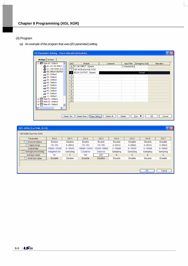
Chapter 8 Programming (XGI, XGR)
8-6
(4) Program
(a) An example of the program that uses [I/O parameter] setting
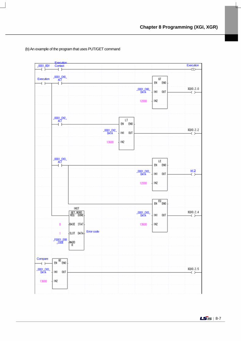
Chapter 8 Programming (XGI, XGR)
8-7
(b) An example of the program that uses PUT/GET command
Execution Contact Execution
Execution
Compare
Error code
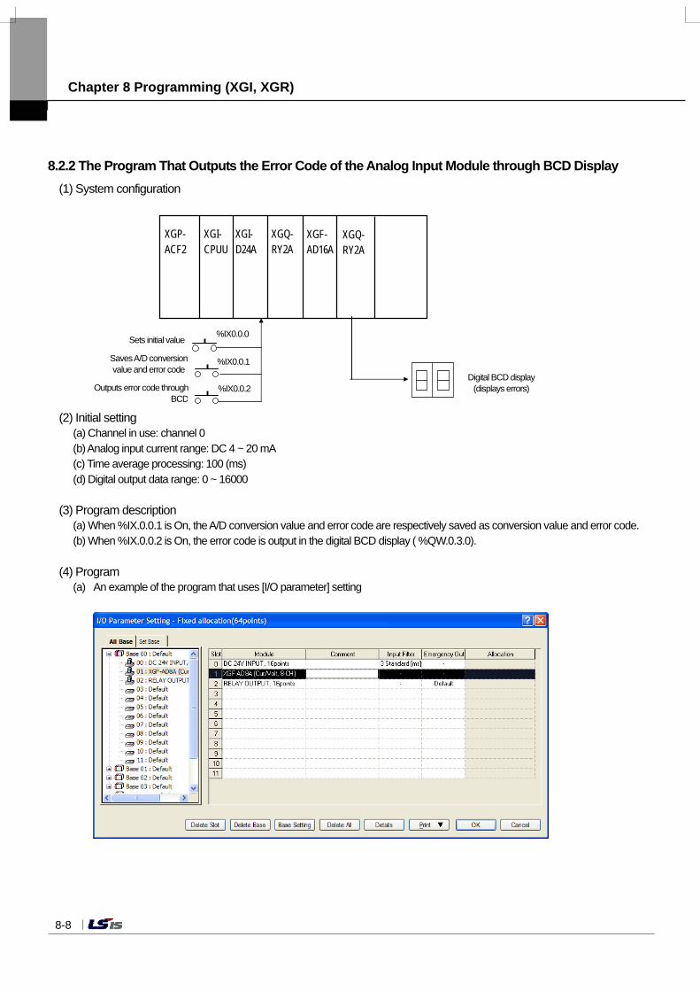
Chapter 8 Programming (XGI, XGR)
8-8
8.2.2 The Program That Outputs the Error Code of the Analog Input Module through BCD Display (1) System configuration
(2) Initial setting
(a) Channel in use: channel 0 (b) Analog input current range: DC 4 ~ 20 mA (c) Time average processing: 100 (ms) (d) Digital output data range: 0 ~ 16000
(3) Program description (a) When %IX.0.0.1 is On, the A/D conversion value and error code are respectively saved as conversion value and error code. (b) When %IX.0.0.2 is On, the error code is output in the digital BCD display ( %QW.0.3.0).
(4) Program
(a) An example of the program that uses [I/O parameter] setting
XGP- ACF2
XGI- CPUU
XGI- D24A
XGQ- RY2A
XGF- AD16A
Digital BCD display (displays errors)
XGQ- RY2A
Sets initial value
Outputs error code throughBCD
Saves A/D conversion value and error code
%IX0.0.0
%IX0.0.1
%IX0.0.2
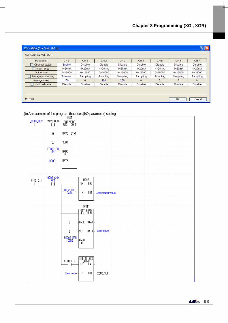
Chapter 8 Programming (XGI, XGR)
8-9
(b) An example of the program that uses [I/O parameter] setting
Conversion value
Error code
Error code
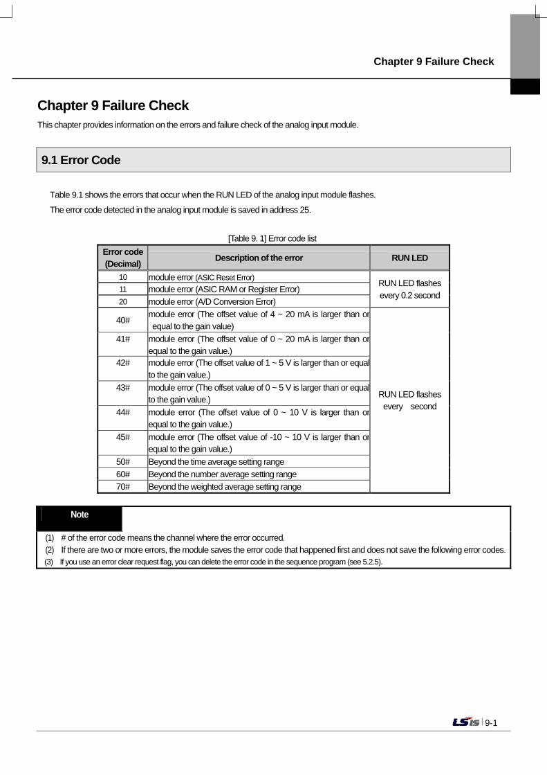
Chapter 9 Failure Check
9-1
Chapter 9 Failure Check This chapter provides information on the errors and failure check of the analog input module.
9.1 Error Code
Table 9.1 shows the errors that occur when the RUN LED of the analog input module flashes.
The error code detected in the analog input module is saved in address 25.
[Table 9. 1] Error code list
Error code (Decimal) Description of the error RUN LED
10 module error (ASIC Reset Error) RUN LED flashes every 0.2 second
11 module error (ASIC RAM or Register Error) 20 module error (A/D Conversion Error)
40# module error (The offset value of 4 ~ 20 mA is larger than or equal to the gain value)
RUN LED flashes every second
41# module error (The offset value of 0 ~ 20 mA is larger than or equal to the gain value.)
42# module error (The offset value of 1 ~ 5 V is larger than or equal to the gain value.)
43# module error (The offset value of 0 ~ 5 V is larger than or equal to the gain value.)
44# module error (The offset value of 0 ~ 10 V is larger than or equal to the gain value.)
45# module error (The offset value of -10 ~ 10 V is larger than or equal to the gain value.)
50# Beyond the time average setting range
60# Beyond the number average setting range
70# Beyond the weighted average setting range
Note (1) # of the error code means the channel where the error occurred. (2) If there are two or more errors, the module saves the error code that happened first and does not save the following error codes.
(3) If you use an error clear request flag, you can delete the error code in the sequence program (see 5.2.5).
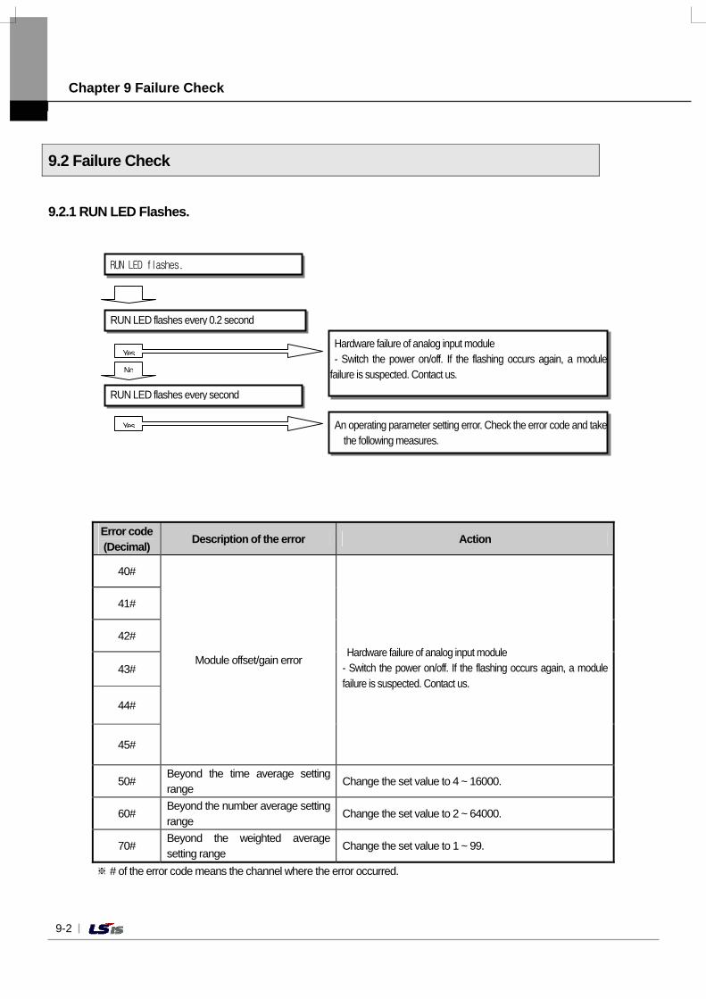
Chapter 9 Failure Check
9-2
9.2 Failure Check
9.2.1 RUN LED Flashes.
Error code (Decimal) Description of the error Action
40#
Module offset/gain error
Hardware failure of analog input module
- Switch the power on/off. If the flashing occurs again, a module failure is suspected. Contact us.
41#
42#
43#
44#
45#
50# Beyond the time average setting range
Change the set value to 4 ~ 16000.
60# Beyond the number average setting range
Change the set value to 2 ~ 64000.
70# Beyond the weighted average setting range
Change the set value to 1 ~ 99.
※ # of the error code means the channel where the error occurred.
RUN LED flashes.
RUN LED flashes every 0.2 second
Hardware failure of analog input module - Switch the power on/off. If the flashing occurs again, a module
failure is suspected. Contact us.
RUN LED flashes every second
An operating parameter setting error. Check the error code and takethe following measures.
Yes
No
Yes
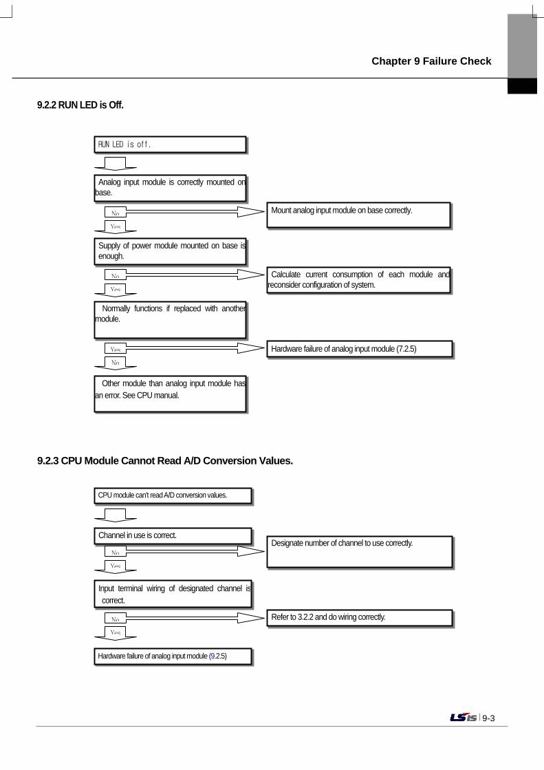
Chapter 9 Failure Check
9-3
9.2.2 RUN LED is Off.
9.2.3 CPU Module Cannot Read A/D Conversion Values.
RUN LED is off.
Analog input module is correctly mounted onbase.
Mount analog input module on base correctly.
Supply of power module mounted on base isenough.
Calculate current consumption of each module and reconsider configuration of system.
Normally functions if replaced with anothermodule.
Other module than analog input module hasan error. See CPU manual.
Hardware failure of analog input module (7.2.5)
No
Yes
No
Yes
Yes
No
CPU module can’t read A/D conversion values.
Channel in use is correct. Designate number of channel to use correctly.
Input terminal wiring of designated channel iscorrect.
Refer to 3.2.2 and do wiring correctly.
Hardware failure of analog input module (9.2.5)
No
Yes
No
Yes
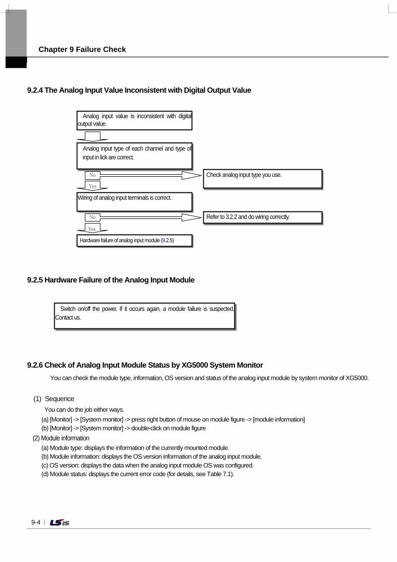
Chapter 9 Failure Check
9-4
9.2.4 The Analog Input Value Inconsistent with Digital Output Value
9.2.5 Hardware Failure of the Analog Input Module
9.2.6 Check of Analog Input Module Status by XG5000 System Monitor You can check the module type, information, OS version and status of the analog input module by system monitor of XG5000.
(1) Sequence
You can do the job either ways.
(a) [Monitor] -> [System monitor] -> press right button of mouse on module figure -> [module information] (b) [Monitor] -> [System monitor] -> double-click on module figure
(2) Module information (a) Module type: displays the information of the currently mounted module. (b) Module information: displays the OS version information of the analog input module. (c) OS version: displays the data when the analog input module OS was configured. (d) Module status: displays the current error code (for details, see Table 7.1).
Switch on/off the power. If it occurs again, a module failure is suspected.Contact us.
Refer to 3.2.2 and do wiring correctly.
Hardware failure of analog input module (9.2.5)
Wiring of analog input terminals is correct.
Analog input type of each channel and type ofinput in lick are correct.
Check analog input type you use. No
Yes
Analog input value is inconsistent with digitaloutput value.
No
Yes
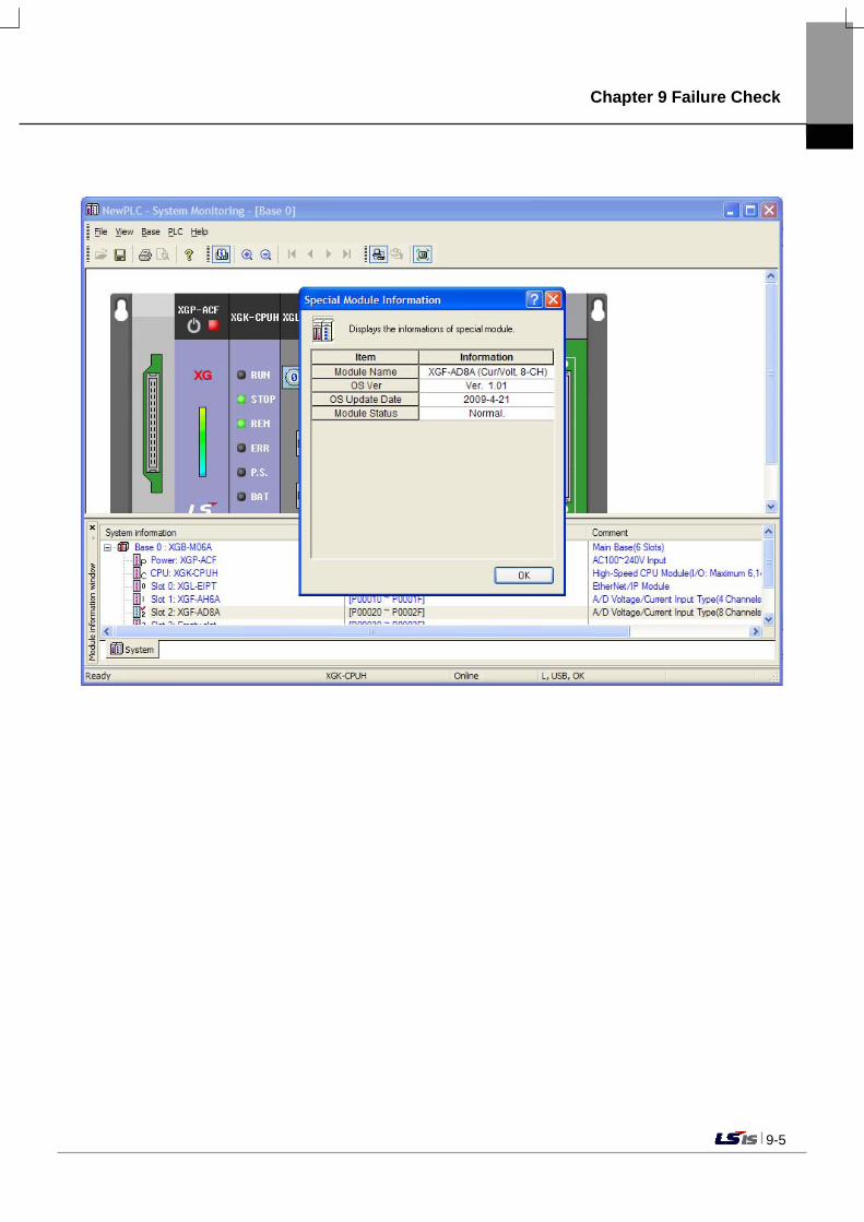
Chapter 9 Failure Check
9-5
Appendix 1. Glossary
A1-1
Appendix 1 Glossary The following glossary covers the manual and the entire analog module. A/D converter: converts the analog input signals into digital values in proportion to the magnitude of the signals. Analog input module: The module that has a circuit which converts analog voltage/current input signals into digital values. It has 14 otr16 bit resolutions according to the converter. Channel: Related to the terminals of the analog input/output module, each channel is linked to various current/voltage input and output devices and has the functions of data and check. Conversion time: The time it takes for the analog input module samples and converts the analog signals and then for the processor in
the module to receive the converted digital values. In addition, this is the time for the digital values from the processor in the module to be converted into analog output signals and transmitted to the output channel.
D/A converter: Performs the function of producing analog voltage and current signals of continuous size in proportion to the digital value. Full scale: The magnitude of voltage and current at which normal function is performed. Full scale error: The difference between an ideal analog conversion value and real analog conversion value on the graph. Full scale range: The difference between the maximum and minimum of the analog inputs. LSB (Least Significant Bit): The minimum of the unit bit line.
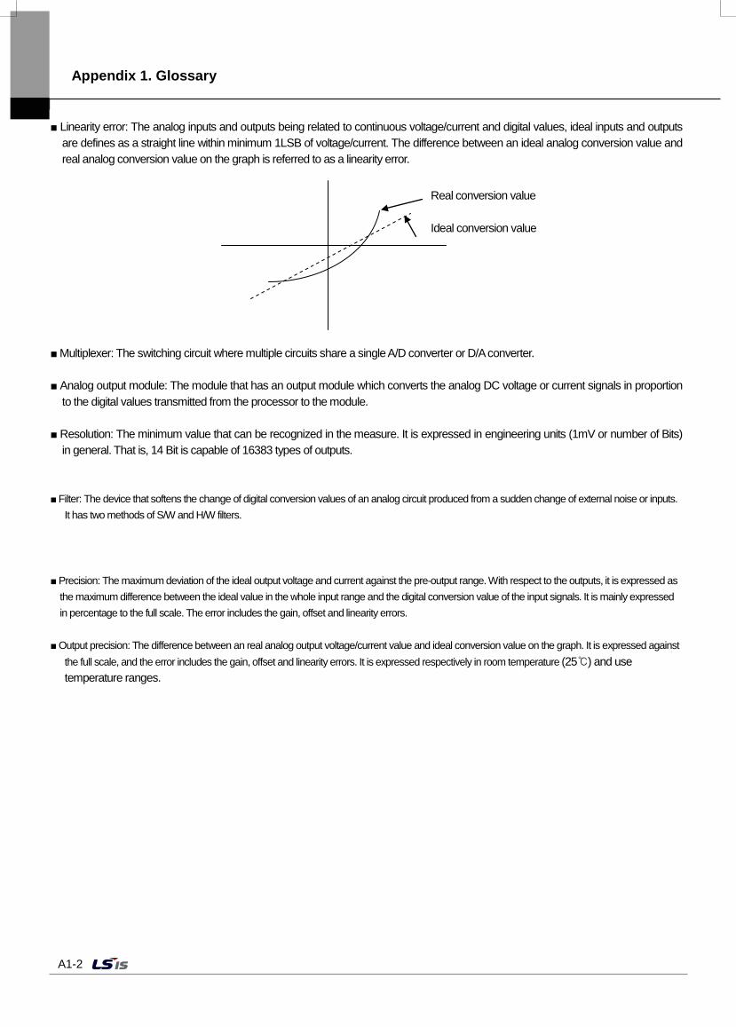
Appendix 1. Glossary
A1-2
Linearity error: The analog inputs and outputs being related to continuous voltage/current and digital values, ideal inputs and outputs are defines as a straight line within minimum 1LSB of voltage/current. The difference between an ideal analog conversion value and real analog conversion value on the graph is referred to as a linearity error.
Multiplexer: The switching circuit where multiple circuits share a single A/D converter or D/A converter. Analog output module: The module that has an output module which converts the analog DC voltage or current signals in proportion
to the digital values transmitted from the processor to the module. Resolution: The minimum value that can be recognized in the measure. It is expressed in engineering units (1mV or number of Bits)
in general. That is, 14 Bit is capable of 16383 types of outputs.
Filter: The device that softens the change of digital conversion values of an analog circuit produced from a sudden change of external noise or inputs. It has two methods of S/W and H/W filters.
Precision: The maximum deviation of the ideal output voltage and current against the pre-output range. With respect to the outputs, it is expressed as the maximum difference between the ideal value in the whole input range and the digital conversion value of the input signals. It is mainly expressed in percentage to the full scale. The error includes the gain, offset and linearity errors.
Output precision: The difference between an real analog output voltage/current value and ideal conversion value on the graph. It is expressed against
the full scale, and the error includes the gain, offset and linearity errors. It is expressed respectively in room temperature (25) and use temperature ranges.
Ideal conversion value
Real conversion value
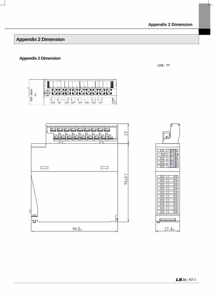
Appendix 2 Dimension
A2-1
Appendix 2 Dimension
Appendix 2 Dimension Unit :
Warranty and Environmental Policy
Warranty 1. Warranty Period
The product you purchased will be guaranteed for 18 months from the date of manufacturing. 2. Scope of Warranty Any trouble or defect occurring for the above-mentioned period will be partially replaced or repaired. However, please note the following
cases will be excluded from the scope of warranty.
(1) Any trouble attributable to unreasonable condition, environment or handling otherwise specified in the manual, (2) Any trouble attributable to others’ products, (3) If the product is modified or repaired in any other place not designated by the company, (4) Due to unintended purposes (5) Owing to the reasons unexpected at the level of the contemporary science and technology when delivered. (6) Not attributable to the company; for instance, natural disasters or fire
3. Since the above warranty is limited to PLC unit only, make sure to use the product considering the safety for system configuration or
applications.
Environmental Policy LS Industrial Systems Co., Ltd supports and observes the environmental policy as below.
LS Industrial Systems considers the environmental preservation as the preferential management subject and every staff of LS Industrial Systems use the reasonable endeavors for the pleasurably environmental preservation of the earth.
LS Industrial Systems’ PLC unit is designed to protect the environment. For the disposal, separate aluminum, iron and synthetic resin (cover) from the product as they are reusable.
Environmental Management About Disposal
HEAD OFFICE LS tower, Hogye-dong, Dongan-gu, Anyang-si, Gyeonggi-do 1026-6,
Korea http://eng.lsis.biz Tel : (82-2)2034-4870/Fax : 82-2-2034-4648 e-mail : [email protected] LSIS Tokyo Office _ Tokyo, Japan
Address: 16FL. Higashi-Kan. Akasaka Twin Tower 17-22, Akasaka.Monato-ku Tokyo 107-8470. Japan Tel : 81-3-3582-9128/Fax : 81-3-3582-2667 e-mail : [email protected] LSIS (ME) FZE _ Dubai, U.A.E.
Address : Jafza View Tower Lob 19, Room 205 Along Sheikh Zayed Road Jebel Aali Free Zone Dubai, United Arab Emirates Tel : 971-4-886-5360/Fax : 971-4-886-5361 e-mail : [email protected]
LSIS Shanghai Office _ Shanghai, China Address : Room E-G. 12FL Hiamin Empire Plaza. No.726. West. Yan'an Road Shanghai 200050. P.R. China e-mail : [email protected]
Tel : 86-21-5237-9977(609)/Fax : 89-21-5237-7189 LSIS Beijing Office _ Beijing, China
Address : B-Tower 17FL. Beijing Global Trade Center B/D. No. 36. East BeisanHuan-Road. DongCheng-District. Beijing 100013. P.R. China
Tel : 86-10-5825-6027(666)/Fax : 86-10-5825-6028 e-mail : [email protected] LSIS Guangzhou Office _ Guangzhou, China
Address : Room 1403.14FL. New Poly Tower. 2 Zhongshan Liu Road.Guangzhou.P.R China Tel : 86-20-8328-6754/Fax : 86-20-8326-6287 e-mail : [email protected]
LSIS Chengdu Office _ Chengdu, China Address : 12FL. Guodong Buiding. No.52 Jindun Road Chengdu.610041. P.R. China Tel : 86-28-8612-9151(9226)/Fax : 86-28-8612-9236 e-mail : [email protected]
LSIS Qingdao Office _ Qingdao, China Address : YinHe Bldg. 402 Room No. 2P Shandong Road, Qingdao-City,Shandong-province 266071, P.R. China Tel : 86-532-8501-6068/Fax : 86-532-8501-6057 e-mail : [email protected]
LSIS Europe B.V. , Netherlands Address : 1st. Floor, Tupolevlaan 48, 1119NZ, Schiphol-Rijk, The Netherlands
Tel : +31 (0)20 654 1420/Fax : +31 (0)20 654 1429 e-mail : [email protected] Wuxi LSIS Co., Ltd _ Wuxi, China
Address : 102-A. National High & New Tech Industrial Development Area. Wuxi. Jiangsu. 214028. P.R. China Tel : 86-510-8534-6666/Fax : 86-510-8534-4078 e-mail : [email protected]
Dalian LSIS Co., Ltd. _ Dalian, China Address : No. 15. Liaohexi 3-Road. Economic and Technical Development zone.
Dalian 116600. China Tel : 86-411-273-7777/Fax : 86-411-8730-7560 e-mail : [email protected]
※ LSIS constantly endeavors to improve its product so that information in this manual is subject to change without notice.
2010 LSIS Co., Ltd All Rights Reserved.
2014. 1
LSIS values every single customers.
Quality and service come first at LSIS.
Always at your service, standing for our customers.
http://www.lsis.com