product note - keysightliterature.cdn.keysight.com/litweb/pdf/5968-5662e.pdfagilent e5500 series...
TRANSCRIPT
Agilent PN E5500-1
Pulsed Carrier Phase NoiseMeasurements Using Agilent E5500 Series SolutionsProduct Note
3
4
22
32
Table of Contents
1. Introduction
2. Making residual (two-port) measurements on pulsed carriersResidual measurement considerations
Hardware configuration
Step-by-step procedure
Example 1: Residual noise floor using an Agilent 83732B
as the source (non-pulsed carrier)
Example 2: Pulsed carrier noise floor using an Agilent
83732B as the stimulus source
Example 3: Residual measurement of an Agilent 8347A
amplifier
3. Making absolute phase noise measurements on pulsed carriersAbsolute phase noise measurement considerations
Hardware configuration
Step-by-step procedure
Example 1: Absolute pulsed measurement—
Agilent 8663A versus Agilent 83732B
Using a microwave downconverter
Example 2: Absolute pulsed measurement using
a microwave downconverter—Agilent 8644B versus
Agilent 83732B
4. Making AM noise measurements on pulsed carriersMeasurement considerations
PRF filtering
Measurement calibration
Example 1: Agilent 83732B pulsed AM noise
measurement using the internal AM detector
3
The sensitivity and usefulness of many wireless
RF and microwave systems is limited by the phase
noise characteristics of their system. In pulsed
radar systems, for example, the phase noise of the
receiver local oscillator sets the minimum signal
level that must be returned from a target for it to
be detected. In this case, phase noise affects the
selectivity of the radar receiver, which in turn deter-
mines the effective range of the overall system.
Since the overall dynamic range of the radar sys-
tem is influenced by the noise of the transmitted
signal, it is important to know not only the absolute
noise of individual oscillators but also the residual
or additive noise of the signal processing devices,
such as power amplifiers and pulse modulators.
In addition, because the final signal in most radar
systems is pulsed, making absolute phase noise
measurements on the pulsed carrier is essential to
determining the overall performance of the system.
This product note discusses the use and limita-
tions of the Agilent Technologies E5500 series
phase noise measurement solutions for making
pulsed carrier phase noise measurements. It
is assumed that the reader is familiar with the
concepts of phase noise and CW phase noise
measurement techniques and with the general
application considerations for measuring pulsed
carrier signals. For a more detailed discussion
of these topics, refer to Agilent Application Note
1309, Pulsed Carrier Phase Noise Measurements (literature number 5968-2081E).
Chapter 2 presents the recommended hardware
configurations and step-by-step measurement
procedure for making residual (two-port) measure-
ments on pulsed RF carriers. Chapter 3 covers
the recommended hardware configurations and
step-by-step measurement procedures for mak-
ing absolute measurements on pulsed carriers.
Chapter 4 is a brief discussion of AM noise meas-
urements with the Agilent E5500 series.
1. Introduction
4
This chapter presents the recommended proce-
dures and hardware configurations for making
residual or two-port phase noise measurements
on pulsed carriers.
Residual measurement considerationsPhase detector selection For carrier frequencies greater than the standard
input frequency range, another phase detector
must be used. This detector may be either an exter-
nal phase detector (whose output would be routed
to the noise input port of the Agilent 70420A phase
noise test set) or an optional internal microwave
phase detector:
Standard (internal) 50 kHz–1.6 GHz
Option 201 (internal) 1.2 GHz–26.5 GHz
Option 001 (internal) 1.2 GHz–26.5 GHz
Path delay differences When making pulsed carrier residual phase noise
measurements, the delay differences between the
two paths will normally not be a concern. If the
PRF (Pulse Repetition Frequency) is high, and
comparisons are being made to non-pulsed or CW
measurements, then the time delay difference in
the two paths between the power splitter and the
phase detector should be kept to a minimum. The
attenuation of the stimulus source’s noise is a
function of offset frequency (f) and the difference
in delay time (∆τ): stimulus source noise attenua-
tion (dB) = 20 log (2 sin (πf ∆τ)). At f = 1/(2π ∆τ)the attenuation goes to 0 dB and at 1/(2 ∆τ), thereis a 6 dB gain.
Measurement noise floor The measurement noise floor represents the lowest
level of noise the system is capable of measuring.
For CW signals, it is set by the noise floor of the
phase detector, the LNA (Low-Noise Amplifier),
and the AM noise feedthrough. Additionally, for
pulsed carrier signals, the duty cycle of the pulsed
signal further degrades the CW noise floor by a
20*log (duty cycle) factor due to a scaling of the
effective detector constant by the duty cycle. The
noise of the phase detector is a function of the sig-
nal power present at the detector input ports. The
recommended power levels (CW or peak) for the
microwave phase detector, to ensure maximum
sensitivity (lowest noise floor), minimum DC offset
and minimum AM noise feedthrough, are +7 to
+10 dBm for the reference input port and 0 to
+5 dBm for the signal input port. The recommended
power levels (CW or peak) for the RF phase detec-
tor are +15 dBm for the reference port input and
+10 dBm for the signal input port.
Source AM noise The stimulus source used for residual measure-
ments must have low AM noise characteristics.
AM noise can cause AM-to-PM conversion within
the DUT (Device Under Test) and it can degrade
the overall measurement system noise floor.
2. Making residual (two-port) measurements on pulsed carriers
5
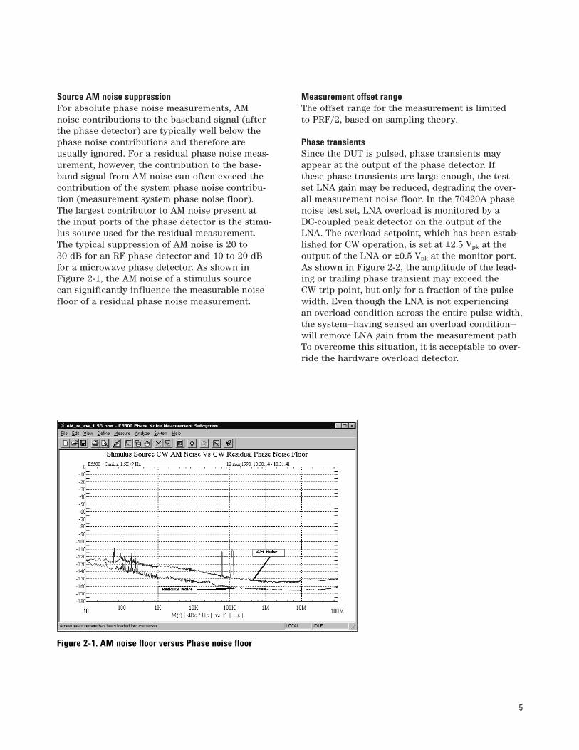
Source AM noise suppression For absolute phase noise measurements, AM
noise contributions to the baseband signal (after
the phase detector) are typically well below the
phase noise contributions and therefore are
usually ignored. For a residual phase noise meas-
urement, however, the contribution to the base-
band signal from AM noise can often exceed the
contribution of the system phase noise contribu-
tion (measurement system phase noise floor).
The largest contributor to AM noise present at
the input ports of the phase detector is the stimu-
lus source used for the residual measurement.
The typical suppression of AM noise is 20 to
30 dB for an RF phase detector and 10 to 20 dB
for a microwave phase detector. As shown in
Figure 2-1, the AM noise of a stimulus source
can significantly influence the measurable noise
floor of a residual phase noise measurement.
Measurement offset range The offset range for the measurement is limited
to PRF/2, based on sampling theory.
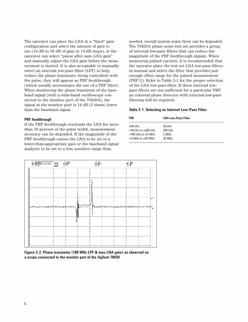
Phase transients Since the DUT is pulsed, phase transients may
appear at the output of the phase detector. If
these phase transients are large enough, the test
set LNA gain may be reduced, degrading the over-
all measurement noise floor. In the 70420A phase
noise test set, LNA overload is monitored by a
DC-coupled peak detector on the output of the
LNA. The overload setpoint, which has been estab-
lished for CW operation, is set at ±2.5 Vpk at the
output of the LNA or ±0.5 Vpk at the monitor port.
As shown in Figure 2-2, the amplitude of the lead-
ing or trailing phase transient may exceed the
CW trip point, but only for a fraction of the pulse
width. Even though the LNA is not experiencing
an overload condition across the entire pulse width,
the system—having sensed an overload condition—
will remove LNA gain from the measurement path.
To overcome this situation, it is acceptable to over-
ride the hardware overload detector.
Figure 2-1. AM noise floor versus Phase noise floor
6
The operator can place the LNA in a “fixed” gain
configuration and select the amount of gain to
use (14 dB to 56 dB of gain in 14-dB steps), or the
operator can select “pause after auto LNA gain”
and manually adjust the LNA gain before the meas-
urement is started. It is also acceptable to manually
select an internal low-pass filter (LPF) to help
reduce the phase transients—being coincident with
the pulse, they will appear as PRF feedthrough
(which usually necessitates the use of a PRF filter).
When monitoring the phase transients of the base-
band signal (with a wide-band oscilloscope con-
nected to the monitor port of the 70420A), the
signal at the monitor port is 14 dB (5 times) lower
than the baseband signal.
PRF feedthrough If the PRF feedthrough overloads the LNA for more
than 10 percent of the pulse width, measurement
accuracy can be degraded. If the magnitude of the
PRF feedthrough causes the LNA to be set to a
lower-than-appropriate gain or the baseband signal
analyzer to be set to a less sensitive range than
needed, overall system noise floor can be degraded.
The 70420A phase noise test set provides a group
of internal low-pass filters that can reduce the
magnitude of the PRF feedthrough signals. When
measuring pulsed carriers, it is recommended that
the operator place the test set LNA low-pass filters
in manual and select the filter that provides just
enough offset range for the pulsed measurement
(PRF/2). Refer to Table 2-1 for the proper selection
of the LNA low-pass filter. If these internal low-
pass filters are not sufficient for a particular PRF,
an external phase detector with external low-pass
filtering will be required.
Table 2-1. Selecting an Internal Low-Pass Filter
PRF LNA Low-Pass Filter
≤40 kHz 20 kHz
>40 kHz to ≤400 kHz 200 kHz
>400 kHz to ≤4 MHz 2 MHz
>4 MHz to ≤40 MHz 20 MHz
Figure 2-2. Phase transients (100 MHz LPF & max LNA gain) as observed on a scope connected to the monitor port of the Agilent 70420
7
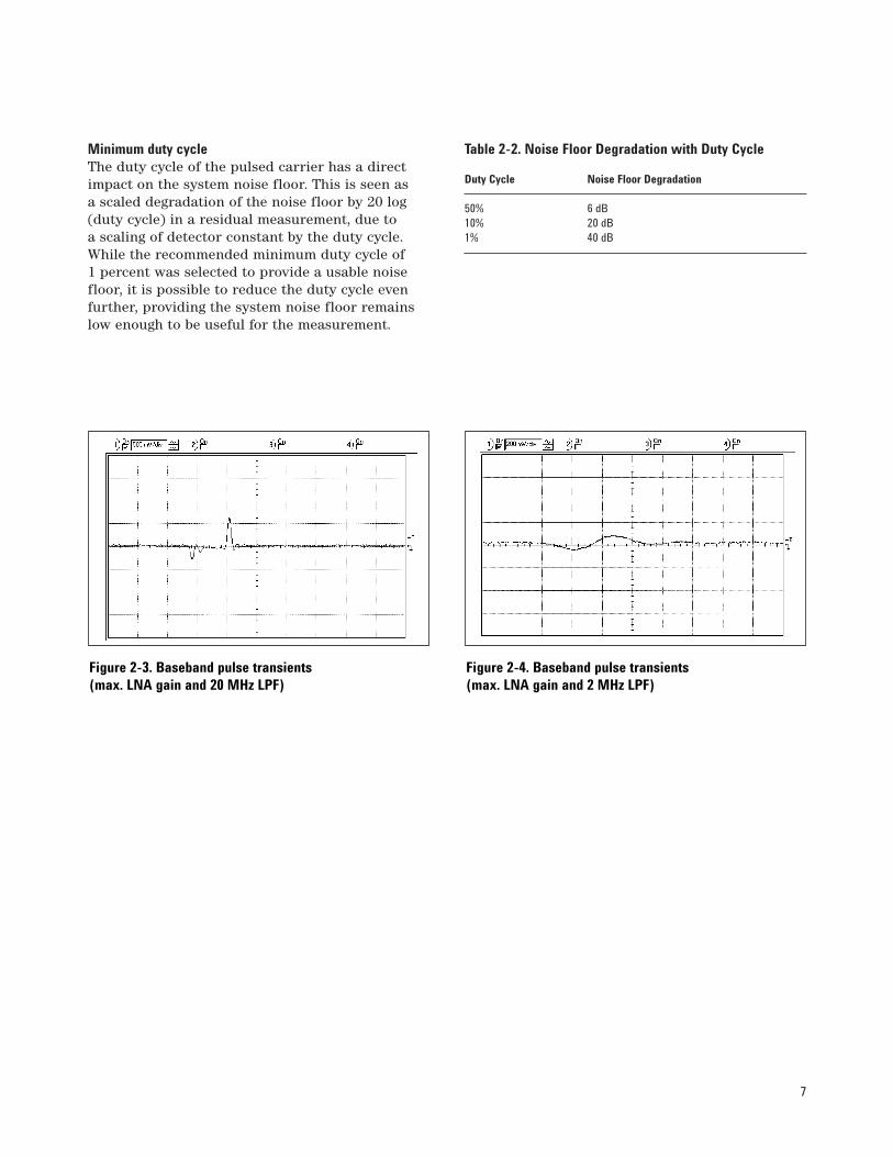
Minimum duty cycle The duty cycle of the pulsed carrier has a direct
impact on the system noise floor. This is seen as
a scaled degradation of the noise floor by 20 log
(duty cycle) in a residual measurement, due to
a scaling of detector constant by the duty cycle.
While the recommended minimum duty cycle of
1 percent was selected to provide a usable noise
floor, it is possible to reduce the duty cycle even
further, providing the system noise floor remains
low enough to be useful for the measurement.
Table 2-2. Noise Floor Degradation with Duty Cycle
Duty Cycle Noise Floor Degradation
50% 6 dB
10% 20 dB
1% 40 dB
Figure 2-3. Baseband pulse transients (max. LNA gain and 20 MHz LPF)
Figure 2-4. Baseband pulse transients(max. LNA gain and 2 MHz LPF)
8
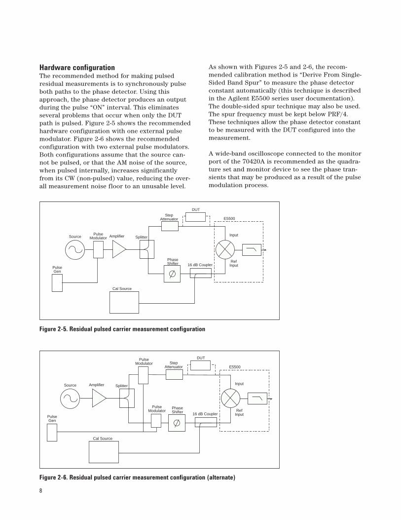
Hardware configurationThe recommended method for making pulsed
residual measurements is to synchronously pulse
both paths to the phase detector. Using this
approach, the phase detector produces an output
during the pulse “ON” interval. This eliminates
several problems that occur when only the DUT
path is pulsed. Figure 2-5 shows the recommended
hardware configuration with one external pulse
modulator. Figure 2-6 shows the recommended
configuration with two external pulse modulators.
Both configurations assume that the source can-
not be pulsed, or that the AM noise of the source,
when pulsed internally, increases significantly
from its CW (non-pulsed) value, reducing the over-
all measurement noise floor to an unusable level.
As shown with Figures 2-5 and 2-6, the recom-
mended calibration method is “Derive From Single-
Sided Band Spur” to measure the phase detector
constant automatically (this technique is described
in the Agilent E5500 series user documentation).
The double-sided spur technique may also be used.
The spur frequency must be kept below PRF/4.
These techniques allow the phase detector constant
to be measured with the DUT configured into the
measurement.
A wide-band oscilloscope connected to the monitor
port of the 70420A is recommended as the quadra-
ture set and monitor device to see the phase tran-
sients that may be produced as a result of the pulse
modulation process.
Figure 2-5. Residual pulsed carrier measurement configuration
Figure 2-6. Residual pulsed carrier measurement configuration (alternate)
PulseGen
Source Splitter
StepAttenuator
DUT
E5500
Input
RefInput
PhaseShifter 16 dB Coupler
Amplifier
Cal Source
PulseModulator
PulseGen
Source
PulseModulator
Splitter
StepAttenuator
DUT
E5500
Input
RefInput
PhaseShifter 16 dB Coupler
Amplifier
Cal Source
PulseModulator
9
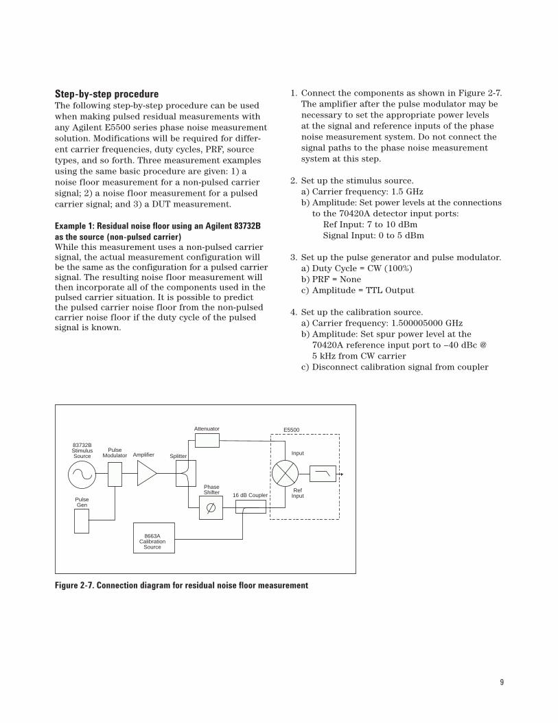
Step-by-step procedureThe following step-by-step procedure can be used
when making pulsed residual measurements with
any Agilent E5500 series phase noise measurement
solution. Modifications will be required for differ-
ent carrier frequencies, duty cycles, PRF, source
types, and so forth. Three measurement examples
using the same basic procedure are given: 1) a
noise floor measurement for a non-pulsed carrier
signal; 2) a noise floor measurement for a pulsed
carrier signal; and 3) a DUT measurement.
Example 1: Residual noise floor using an Agilent 83732Bas the source (non-pulsed carrier)While this measurement uses a non-pulsed carrier
signal, the actual measurement configuration will
be the same as the configuration for a pulsed carrier
signal. The resulting noise floor measurement will
then incorporate all of the components used in the
pulsed carrier situation. It is possible to predict
the pulsed carrier noise floor from the non-pulsed
carrier noise floor if the duty cycle of the pulsed
signal is known.
1. Connect the components as shown in Figure 2-7.
The amplifier after the pulse modulator may be
necessary to set the appropriate power levels
at the signal and reference inputs of the phase
noise measurement system. Do not connect the
signal paths to the phase noise measurement
system at this step.
2. Set up the stimulus source.
a) Carrier frequency: 1.5 GHz
b) Amplitude: Set power levels at the connections
to the 70420A detector input ports:
Ref Input: 7 to 10 dBm
Signal Input: 0 to 5 dBm
3. Set up the pulse generator and pulse modulator.
a) Duty Cycle = CW (100%)
b) PRF = None
c) Amplitude = TTL Output
4. Set up the calibration source.
a) Carrier frequency: 1.500005000 GHz
b) Amplitude: Set spur power level at the
70420A reference input port to –40 dBc @
5 kHz from CW carrier
c) Disconnect calibration signal from coupler
Figure 2-7. Connection diagram for residual noise floor measurement
PulseGen
83732BStimulusSource
PulseModulator Splitter
Attenuator E5500
Input
RefInput
PhaseShifter 16 dB Coupler
Amplifier
8663ACalibration
Source
10
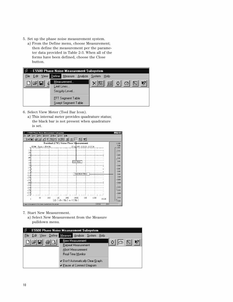
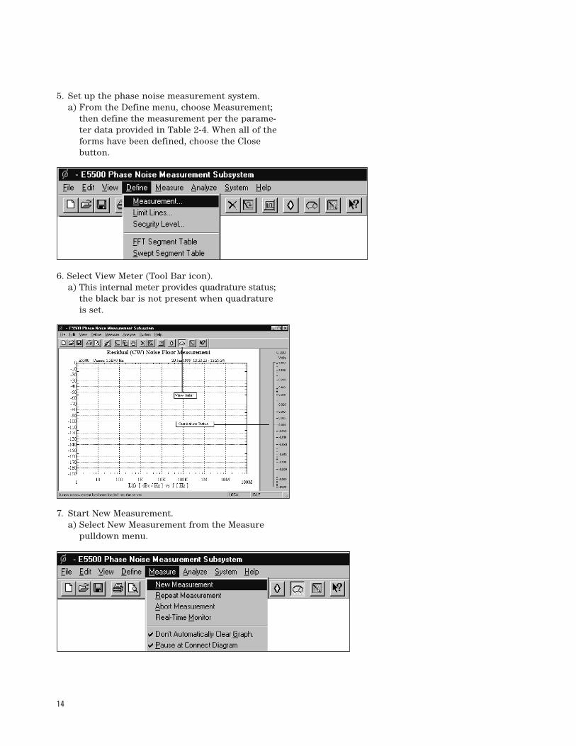
5. Set up the phase noise measurement system.
a) From the Define menu, choose Measurement;
then define the measurement per the parame-
ter data provided in Table 2-3. When all of the
forms have been defined, choose the Close
button.
6. Select View Meter (Tool Bar Icon).
a) This internal meter provides quadrature status;
the black bar is not present when quadrature
is set.
7. Start New Measurement.
a) Select New Measurement from the Measure
pulldown menu.
11
b) When the connect diagram is displayed, check
hardware and connections.
1) Connect scope to monitor port of 70420A
test set.
2) Set scope to monitor waveform.
3) Connect the signal paths to the phase noise
test set.
4) Set quadrature (set the signal to zero volts
on scope and a null on View Meter).
c) Select Continue.
d) When prompted by the software, connect the
calibration signal from the calibration source
to the coupler, then select Continue.
e) When prompted by the software, disconnect
the calibration signal from the calibration
source, then select Continue.
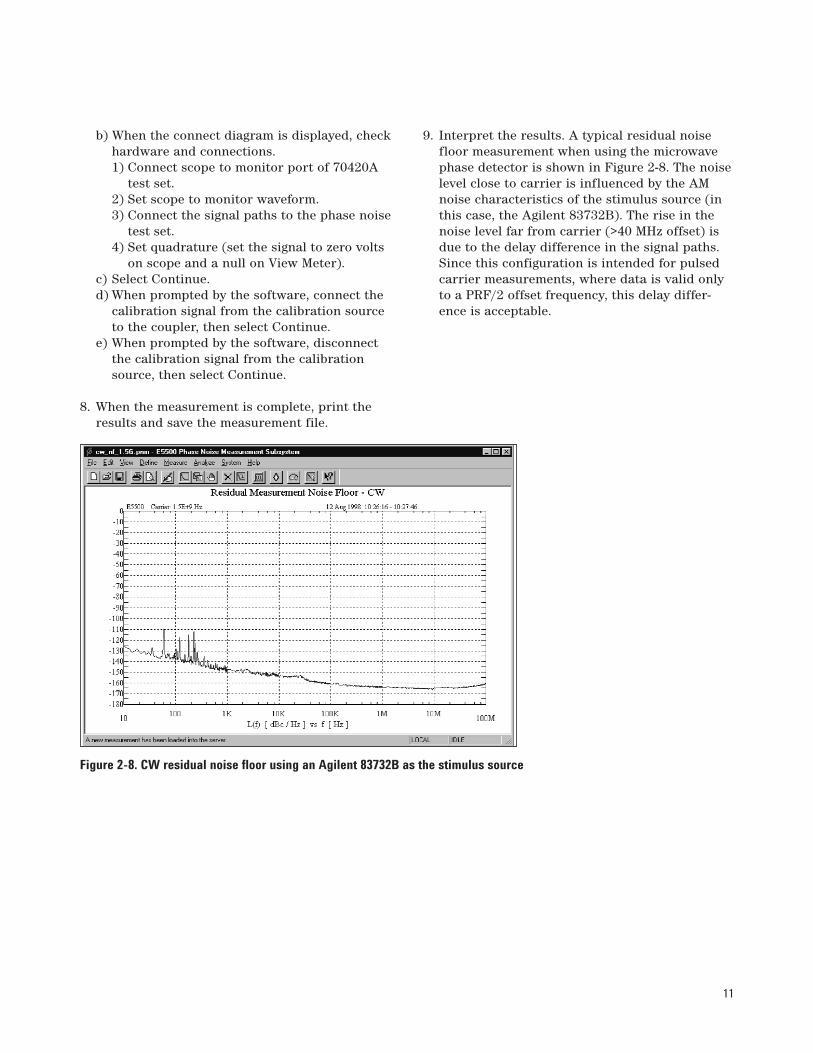
8. When the measurement is complete, print the
results and save the measurement file.
9. Interpret the results. A typical residual noise
floor measurement when using the microwave
phase detector is shown in Figure 2-8. The noise
level close to carrier is influenced by the AM
noise characteristics of the stimulus source (in
this case, the Agilent 83732B). The rise in the
noise level far from carrier (>40 MHz offset) is
due to the delay difference in the signal paths.
Since this configuration is intended for pulsed
carrier measurements, where data is valid only
to a PRF/2 offset frequency, this delay differ-
ence is acceptable.
Figure 2-8. CW residual noise floor using an Agilent 83732B as the stimulus source
12
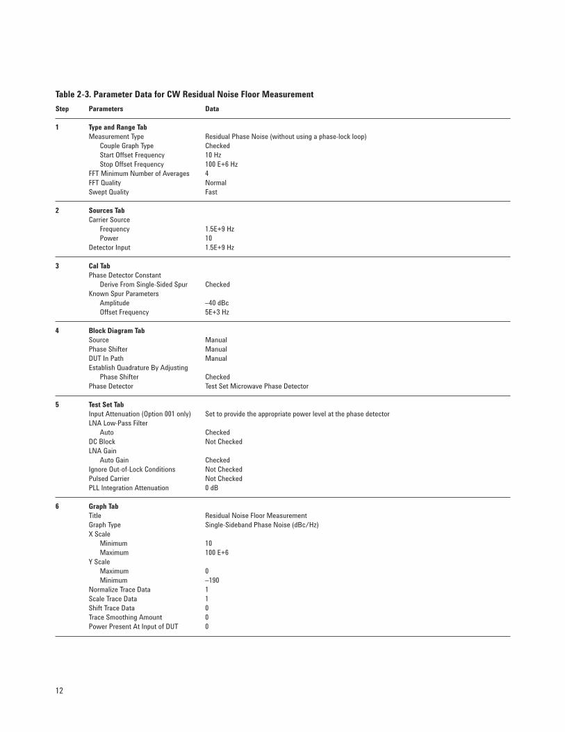
Table 2-3. Parameter Data for CW Residual Noise Floor Measurement
Step Parameters Data
1 Type and Range TabMeasurement Type Residual Phase Noise (without using a phase-lock loop)
Couple Graph Type Checked
Start Offset Frequency 10 Hz
Stop Offset Frequency 100 E+6 Hz
FFT Minimum Number of Averages 4
FFT Quality Normal
Swept Quality Fast
2 Sources TabCarrier Source
Frequency 1.5E+9 Hz
Power 10
Detector Input 1.5E+9 Hz
3 Cal TabPhase Detector Constant
Derive From Single-Sided Spur Checked
Known Spur Parameters
Amplitude –40 dBc
Offset Frequency 5E+3 Hz
4 Block Diagram TabSource Manual
Phase Shifter Manual
DUT In Path Manual
Establish Quadrature By Adjusting
Phase Shifter Checked
Phase Detector Test Set Microwave Phase Detector
5 Test Set TabInput Attenuation (Option 001 only) Set to provide the appropriate power level at the phase detector
LNA Low-Pass Filter
Auto Checked
DC Block Not Checked
LNA Gain
Auto Gain Checked
Ignore Out-of-Lock Conditions Not Checked
Pulsed Carrier Not Checked
PLL Integration Attenuation 0 dB
6 Graph TabTitle Residual Noise Floor Measurement
Graph Type Single-Sideband Phase Noise (dBc/Hz)
X Scale
Minimum 10
Maximum 100 E+6
Y Scale
Maximum 0
Minimum –190
Normalize Trace Data 1
Scale Trace Data 1
Shift Trace Data 0
Trace Smoothing Amount 0
Power Present At Input of DUT 0
13
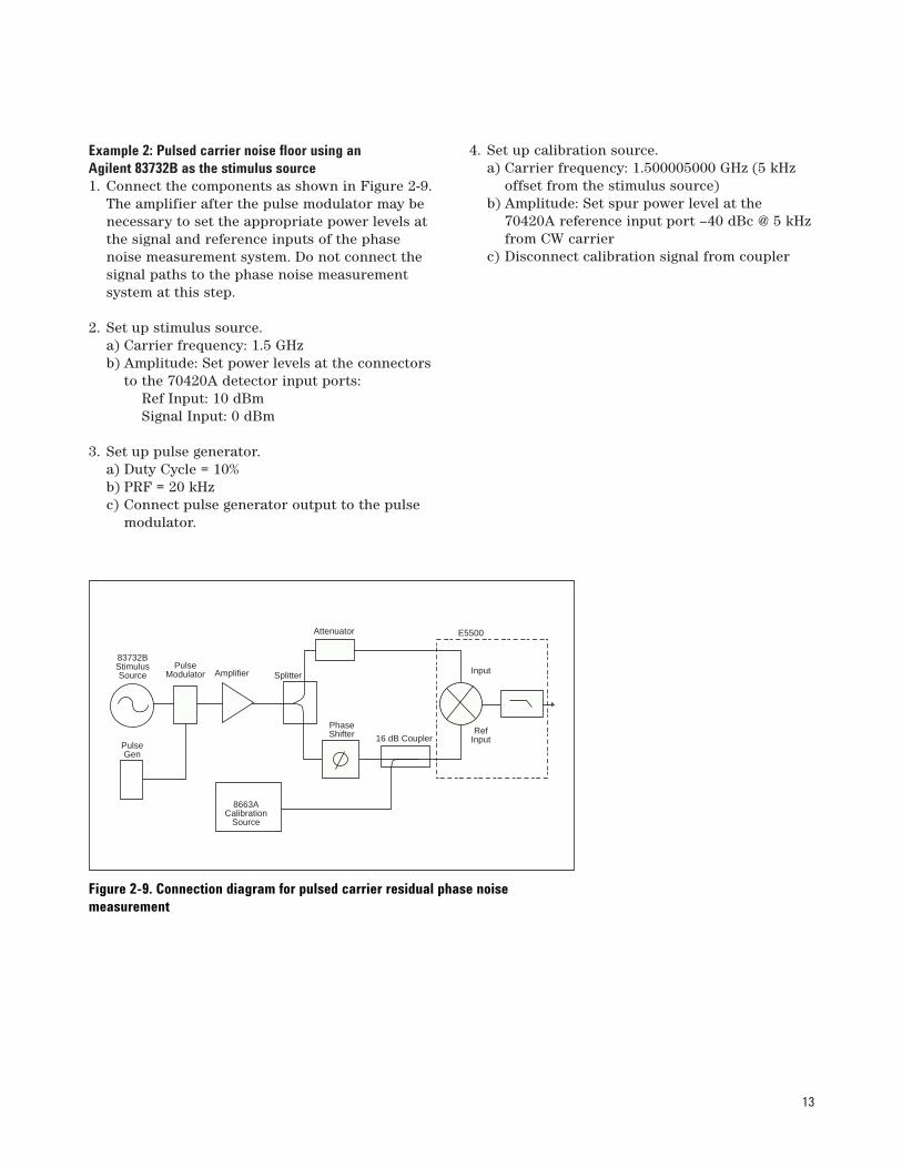
Example 2: Pulsed carrier noise floor using an Agilent 83732B as the stimulus source1. Connect the components as shown in Figure 2-9.
The amplifier after the pulse modulator may be
necessary to set the appropriate power levels at
the signal and reference inputs of the phase
noise measurement system. Do not connect the
signal paths to the phase noise measurement
system at this step.
2. Set up stimulus source.
a) Carrier frequency: 1.5 GHz
b) Amplitude: Set power levels at the connectors
to the 70420A detector input ports:
Ref Input: 10 dBm
Signal Input: 0 dBm
3. Set up pulse generator.
a) Duty Cycle = 10%
b) PRF = 20 kHz
c) Connect pulse generator output to the pulse
modulator.
4. Set up calibration source.
a) Carrier frequency: 1.500005000 GHz (5 kHz
offset from the stimulus source)
b) Amplitude: Set spur power level at the
70420A reference input port –40 dBc @ 5 kHz
from CW carrier
c) Disconnect calibration signal from coupler
PulseGen
83732BStimulusSource
PulseModulator Splitter
Attenuator E5500
Input
RefInput
PhaseShifter 16 dB Coupler
Amplifier
8663ACalibration
Source
Figure 2-9. Connection diagram for pulsed carrier residual phase noise measurement
14
5. Set up the phase noise measurement system.
a) From the Define menu, choose Measurement;
then define the measurement per the parame-
ter data provided in Table 2-4. When all of the
forms have been defined, choose the Close
button.
6. Select View Meter (Tool Bar icon).
a) This internal meter provides quadrature status;
the black bar is not present when quadrature
is set.
7. Start New Measurement.
a) Select New Measurement from the Measure
pulldown menu.
15
b) When the connect diagram is displayed, check
hardware and connections.
1) Connect scope to monitor port of 70420A
test set.
2) Set scope to monitor waveform.
3) Connect the signal paths to the phase noise
test set.
4) Set quadrature (set the signal to zero volts
on scope and a null on View Meter).
c) Select Continue.
d) When prompted by the software, connect the
calibration signal from the calibration source
to the coupler, then select Continue.
e) When prompted by the software, disconnect
the calibration signal from the calibration
source, then select Continue.
8. When the measurement is complete, print the
results and save the measurement file.
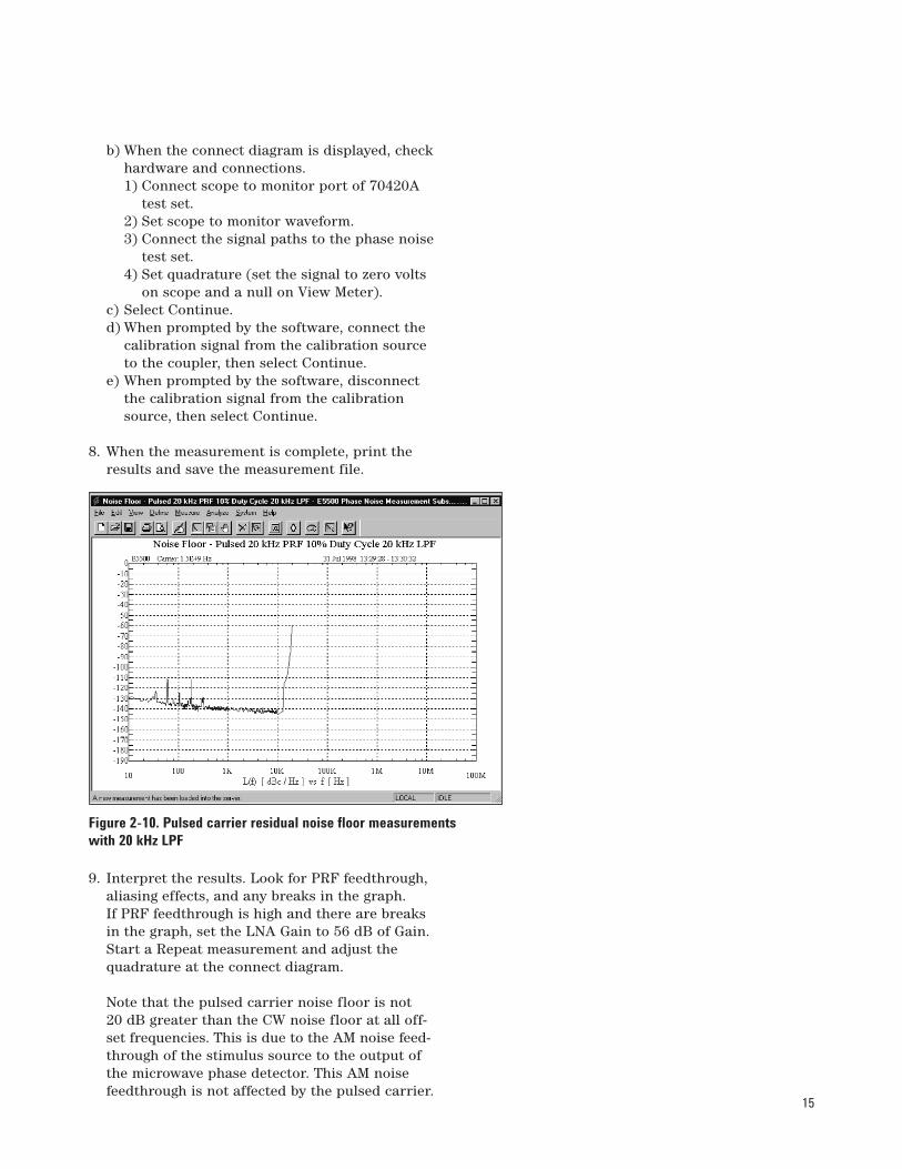
9. Interpret the results. Look for PRF feedthrough,
aliasing effects, and any breaks in the graph.
If PRF feedthrough is high and there are breaks
in the graph, set the LNA Gain to 56 dB of Gain.
Start a Repeat measurement and adjust the
quadrature at the connect diagram.
Note that the pulsed carrier noise floor is not
20 dB greater than the CW noise floor at all off-
set frequencies. This is due to the AM noise feed-
through of the stimulus source to the output of
the microwave phase detector. This AM noise
feedthrough is not affected by the pulsed carrier.
Figure 2-10. Pulsed carrier residual noise floor measurements with 20 kHz LPF
16
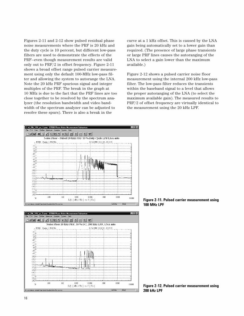
Figures 2-11 and 2-12 show pulsed residual phase
noise measurements where the PRF is 20 kHz and
the duty cycle is 10 percent, but different low-pass
filters are used to demonstrate the effects of the
PRF—even though measurement results are valid
only out to PRF/2 in offset frequency. Figure 2-11
shows a broad offset range pulsed carrier measure-
ment using only the default 100-MHz low-pass fil-
ter and allowing the system to autorange the LNA.
Note the 20 kHz PRF spurious signal and integer
multiples of the PRF. The break in the graph at
10 MHz is due to the fact that the PRF lines are too
close together to be resolved by the spectrum ana-
lyzer (the resolution bandwidth and video band-
width of the spectrum analyzer can be adjusted to
resolve these spurs). There is also a break in the
curve at a 1 kHz offset. This is caused by the LNA
gain being automatically set to a lower gain than
required. (The presence of large phase transients
or large PRF lines causes the autoranging of the
LNA to select a gain lower than the maximum
available.)
Figure 2-12 shows a pulsed carrier noise floor
measurement using the internal 200 kHz low-pass
filter. The low-pass filter reduces the transients
within the baseband signal to a level that allows
the proper autoranging of the LNA (to select the
maximum available gain). The measured results to
PRF/2 of offset frequency are virtually identical to
the measurement using the 20 kHz LPF.
Figure 2-11. Pulsed carrier measurement using100 MHz LPF
Figure 2-12. Pulsed carrier measurement using200 kHz LPF
17
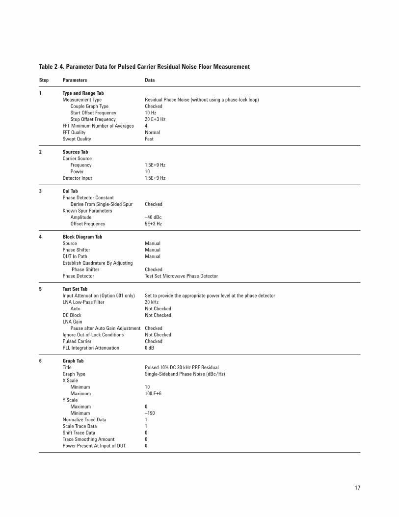
Table 2-4. Parameter Data for Pulsed Carrier Residual Noise Floor Measurement
Step Parameters Data
1 Type and Range TabMeasurement Type Residual Phase Noise (without using a phase-lock loop)
Couple Graph Type Checked
Start Offset Frequency 10 Hz
Stop Offset Frequency 20 E+3 Hz
FFT Minimum Number of Averages 4
FFT Quality Normal
Swept Quality Fast
2 Sources TabCarrier Source
Frequency 1.5E+9 Hz
Power 10
Detector Input 1.5E+9 Hz
3 Cal TabPhase Detector Constant
Derive From Single-Sided Spur Checked
Known Spur Parameters
Amplitude –40 dBc
Offset Frequency 5E+3 Hz
4 Block Diagram TabSource Manual
Phase Shifter Manual
DUT In Path Manual
Establish Quadrature By Adjusting
Phase Shifter Checked
Phase Detector Test Set Microwave Phase Detector
5 Test Set TabInput Attenuation (Option 001 only) Set to provide the appropriate power level at the phase detector
LNA Low-Pass Filter 20 kHz
Auto Not Checked
DC Block Not Checked
LNA Gain
Pause after Auto Gain Adjustment Checked
Ignore Out-of-Lock Conditions Not Checked
Pulsed Carrier Checked
PLL Integration Attenuation 0 dB
6 Graph TabTitle Pulsed 10% DC 20 kHz PRF Residual
Graph Type Single-Sideband Phase Noise (dBc/Hz)
X Scale
Minimum 10
Maximum 100 E+6
Y Scale
Maximum 0
Minimum –190
Normalize Trace Data 1
Scale Trace Data 1
Shift Trace Data 0
Trace Smoothing Amount 0
Power Present At Input of DUT 0
18
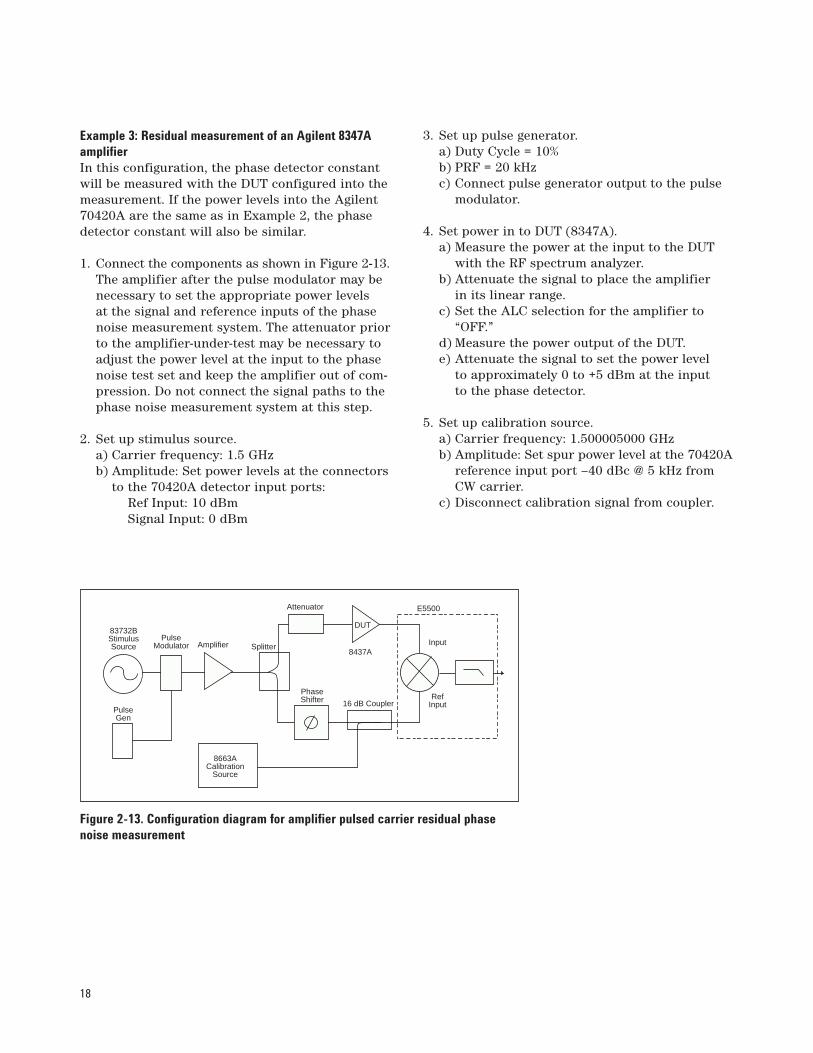
Example 3: Residual measurement of an Agilent 8347Aamplifier In this configuration, the phase detector constant
will be measured with the DUT configured into the
measurement. If the power levels into the Agilent
70420A are the same as in Example 2, the phase
detector constant will also be similar.
1. Connect the components as shown in Figure 2-13.
The amplifier after the pulse modulator may be
necessary to set the appropriate power levels
at the signal and reference inputs of the phase
noise measurement system. The attenuator prior
to the amplifier-under-test may be necessary to
adjust the power level at the input to the phase
noise test set and keep the amplifier out of com-
pression. Do not connect the signal paths to the
phase noise measurement system at this step.
2. Set up stimulus source.
a) Carrier frequency: 1.5 GHz
b) Amplitude: Set power levels at the connectors
to the 70420A detector input ports:
Ref Input: 10 dBm
Signal Input: 0 dBm
3. Set up pulse generator.
a) Duty Cycle = 10%
b) PRF = 20 kHz
c) Connect pulse generator output to the pulse
modulator.
4. Set power in to DUT (8347A).
a) Measure the power at the input to the DUT
with the RF spectrum analyzer.
b) Attenuate the signal to place the amplifier
in its linear range.
c) Set the ALC selection for the amplifier to
“OFF.”
d) Measure the power output of the DUT.
e) Attenuate the signal to set the power level
to approximately 0 to +5 dBm at the input
to the phase detector.
5. Set up calibration source.
a) Carrier frequency: 1.500005000 GHz
b) Amplitude: Set spur power level at the 70420A
reference input port –40 dBc @ 5 kHz from
CW carrier.
c) Disconnect calibration signal from coupler.
Figure 2-13. Configuration diagram for amplifier pulsed carrier residual phasenoise measurement
PulseGen
83732BStimulusSource
PulseModulator Splitter
Attenuator E5500
8437AInput
RefInput
PhaseShifter 16 dB Coupler
Amplifier
8663ACalibration
Source
DUT
19
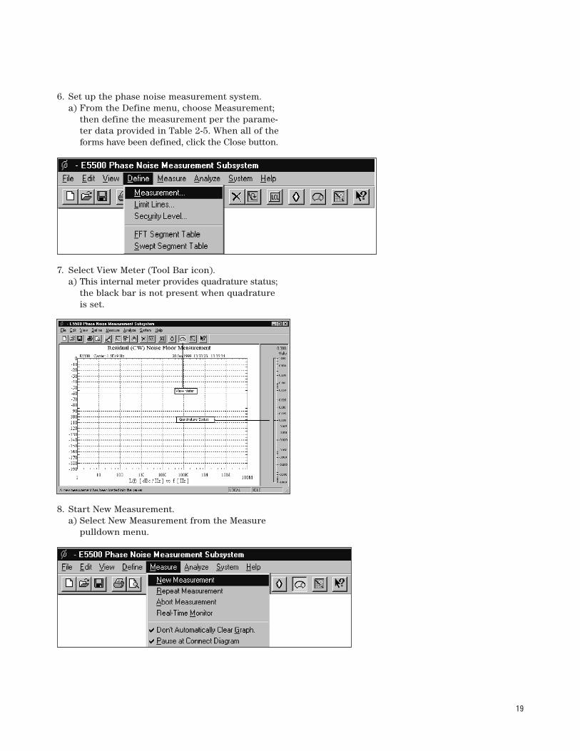
6. Set up the phase noise measurement system.
a) From the Define menu, choose Measurement;
then define the measurement per the parame-
ter data provided in Table 2-5. When all of the
forms have been defined, click the Close button.
7. Select View Meter (Tool Bar icon).
a) This internal meter provides quadrature status;
the black bar is not present when quadrature
is set.
8. Start New Measurement.
a) Select New Measurement from the Measure
pulldown menu.
20
b) When the connect diagram is displayed,
check hardware and connections.
1) Connect scope to monitor port of 70420A
test set.
2) Set scope to monitor waveform.
3) Connect the signal paths to the phase noise
test set.
4) Set quadrature (set the signal to zero volts
on scope and a null on View Meter).
c) Select Continue.
d) When prompted by the software, connect the
calibration signal from the calibration source
to the coupler, then select Continue.
e) When prompted by the software, disconnect
the calibration signal from the calibration
source, then select Continue.
8. When the measurement is complete, print the
results and save the measurement file.
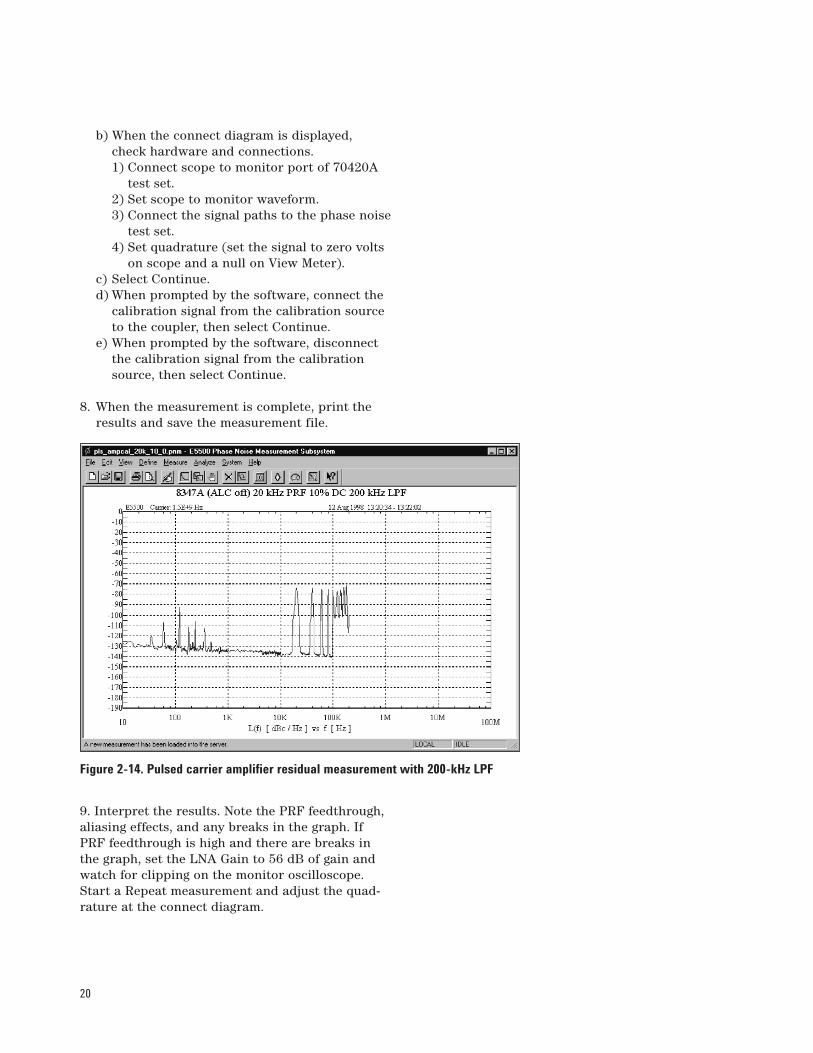
9. Interpret the results. Note the PRF feedthrough,
aliasing effects, and any breaks in the graph. If
PRF feedthrough is high and there are breaks in
the graph, set the LNA Gain to 56 dB of gain and
watch for clipping on the monitor oscilloscope.
Start a Repeat measurement and adjust the quad-
rature at the connect diagram.
Figure 2-14. Pulsed carrier amplifier residual measurement with 200-kHz LPF

21
Table 2-5. Parameter Data for Pulsed Carrier Amplifier Residual Measurement
Step Parameters Data
1 Type and Range TabMeasurement Type Residual Phase Noise (without using a phase-lock loop)
Couple Graph Type Checked
Start Offset Frequency 10 Hz
Stop Offset Frequency 200 E+3 Hz
FFT Minimum Number of Averages 4
FFT Quality Normal
Swept Quality Fast
2 Sources TabCarrier Source
Frequency 1.5E+9 Hz
Power 10
Detector Input 1.5E+9 Hz
3 Cal TabPhase Detector Constant
Derive From Single-Sided Spur Checked
Known Spur Parameters
Amplitude –40 dBc
Offset Frequency 5E+3 Hz
4 Block Diagram TabSource Manual
Phase Shifter Manual
DUT In Path Manual
Establish Quadrature By Adjusting
Phase Shifter Checked
Phase Detector Test Set Microwave Phase Detector
5 Test Set TabInput Attenuation (Option 001 only) Set to provide the appropriate power level at the phase detector
LNA Low-Pass Filter 200 kHz
Auto Not Checked
DC Block Not Checked
LNA Gain
Pause after Auto Gain Adjustment Checked
Ignore Out-of-Lock Conditions Not Checked
Pulsed Carrier Checked
PLL Integration Attenuation 0 dB
6 Graph TabTitle 8347A (ALC Off) 20 kHz PRF 10% DC 200 kHz LPF
Graph Type Single-Sideband Phase Noise (dBc/Hz)
X Scale
Minimum 10
Maximum 100 E+6
Y Scale
Maximum 0
Minimum –190
Normalize Trace Data 1
Scale Trace Data 1
Shift Trace Data 0
Trace Smoothing Amount 0
Power Present At Input of DUT 0
22
This chapter presents the recommended proce-
dures and hardware configurations for making
absolute phase noise measurements on pulsed
carriers. For a complete description of how
pulsing the carrier affects phase noise measure-
ments, refer to Agilent Application Note 1309
Pulsed Carrier Phase Noise Measurements(literature number 5968-2081E).
Absolute phase noise measurement considerationsMeasurement noise floor The measurement noise floor represents the
lowest level of noise the system is capable of
measuring. For CW signals, it is set by the noise
of the test set (phase detector and LNA), the noise
of the comparison reference oscillator, the noise
of the microwave downconverter, or a combination
of all three—provided sufficient power is available
at the phase detector input ports. Additionally, for
pulsed carrier signals, the duty cycle of the pulsed
signal further degrades the CW test set noise floor
by a 20*log (duty cycle) factor. The recommended
power levels for the microwave phase detector are
+7 to +10 dBm for the reference input port and
0 to +5 dBm for the signal input port. The recom-
mended power levels (CW or peak) for the RF phase
detector are +15 to +23 dBm for the reference input
port and 0 to +15 dBm for the signal input port.
Measurement offset range The offset range for the measurement is limited
to PRF/2, based on sampling theory.
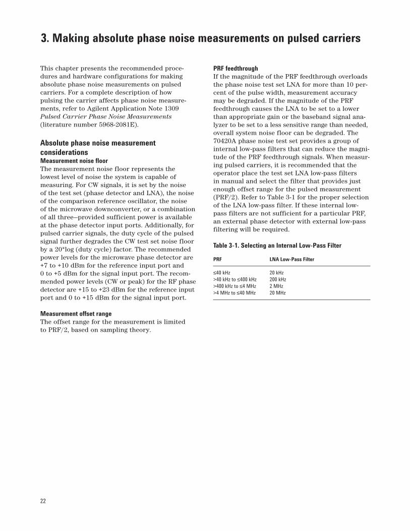
PRF feedthrough If the magnitude of the PRF feedthrough overloads
the phase noise test set LNA for more than 10 per-
cent of the pulse width, measurement accuracy
may be degraded. If the magnitude of the PRF
feedthrough causes the LNA to be set to a lower
than appropriate gain or the baseband signal ana-
lyzer to be set to a less sensitive range than needed,
overall system noise floor can be degraded. The
70420A phase noise test set provides a group of
internal low-pass filters that can reduce the magni-
tude of the PRF feedthrough signals. When measur-
ing pulsed carriers, it is recommended that the
operator place the test set LNA low-pass filters
in manual and select the filter that provides just
enough offset range for the pulsed measurement
(PRF/2). Refer to Table 3-1 for the proper selection
of the LNA low-pass filter. If these internal low-
pass filters are not sufficient for a particular PRF,
an external phase detector with external low-pass
filtering will be required.
Table 3-1. Selecting an Internal Low-Pass Filter
PRF LNA Low-Pass Filter
≤40 kHz 20 kHz
>40 kHz to ≤400 kHz 200 kHz
>400 kHz to ≤4 MHz 2 MHz
>4 MHz to ≤40 MHz 20 MHz
3. Making absolute phase noise measurements on pulsed carriers
23
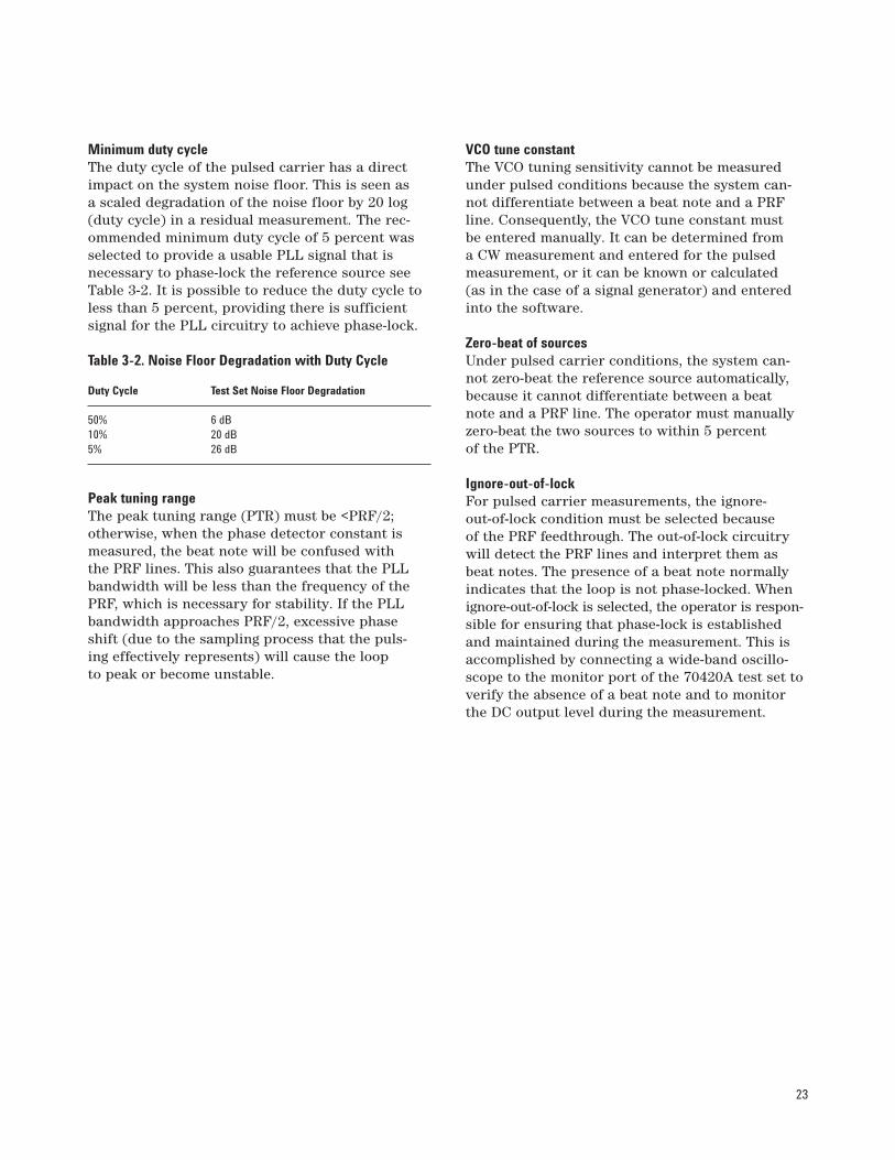
Minimum duty cycle The duty cycle of the pulsed carrier has a direct
impact on the system noise floor. This is seen as
a scaled degradation of the noise floor by 20 log
(duty cycle) in a residual measurement. The rec-
ommended minimum duty cycle of 5 percent was
selected to provide a usable PLL signal that is
necessary to phase-lock the reference source see
Table 3-2. It is possible to reduce the duty cycle to
less than 5 percent, providing there is sufficient
signal for the PLL circuitry to achieve phase-lock.
Table 3-2. Noise Floor Degradation with Duty Cycle
Duty Cycle Test Set Noise Floor Degradation
50% 6 dB
10% 20 dB
5% 26 dB
Peak tuning range The peak tuning range (PTR) must be <PRF/2;
otherwise, when the phase detector constant is
measured, the beat note will be confused with
the PRF lines. This also guarantees that the PLL
bandwidth will be less than the frequency of the
PRF, which is necessary for stability. If the PLL
bandwidth approaches PRF/2, excessive phase
shift (due to the sampling process that the puls-
ing effectively represents) will cause the loop
to peak or become unstable.
VCO tune constant The VCO tuning sensitivity cannot be measured
under pulsed conditions because the system can-
not differentiate between a beat note and a PRF
line. Consequently, the VCO tune constant must
be entered manually. It can be determined from
a CW measurement and entered for the pulsed
measurement, or it can be known or calculated
(as in the case of a signal generator) and entered
into the software.
Zero-beat of sources Under pulsed carrier conditions, the system can-
not zero-beat the reference source automatically,
because it cannot differentiate between a beat
note and a PRF line. The operator must manually
zero-beat the two sources to within 5 percent
of the PTR.
Ignore-out-of-lockFor pulsed carrier measurements, the ignore-
out-of-lock condition must be selected because
of the PRF feedthrough. The out-of-lock circuitry
will detect the PRF lines and interpret them as
beat notes. The presence of a beat note normally
indicates that the loop is not phase-locked. When
ignore-out-of-lock is selected, the operator is respon-
sible for ensuring that phase-lock is established
and maintained during the measurement. This is
accomplished by connecting a wide-band oscillo-
scope to the monitor port of the 70420A test set to
verify the absence of a beat note and to monitor
the DC output level during the measurement.
24
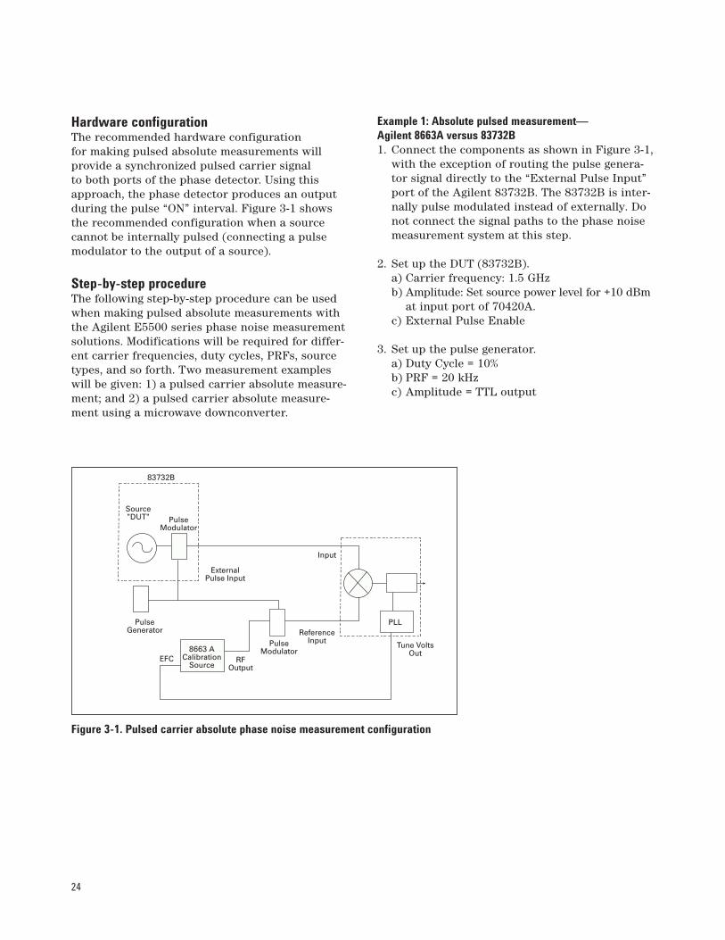
Hardware configurationThe recommended hardware configuration
for making pulsed absolute measurements will
provide a synchronized pulsed carrier signal
to both ports of the phase detector. Using this
approach, the phase detector produces an output
during the pulse “ON” interval. Figure 3-1 shows
the recommended configuration when a source
cannot be internally pulsed (connecting a pulse
modulator to the output of a source).
Step-by-step procedureThe following step-by-step procedure can be used
when making pulsed absolute measurements with
the Agilent E5500 series phase noise measurement
solutions. Modifications will be required for differ-
ent carrier frequencies, duty cycles, PRFs, source
types, and so forth. Two measurement examples
will be given: 1) a pulsed carrier absolute measure-
ment; and 2) a pulsed carrier absolute measure-
ment using a microwave downconverter.
Example 1: Absolute pulsed measurement—Agilent 8663A versus 83732B 1. Connect the components as shown in Figure 3-1,
with the exception of routing the pulse genera-
tor signal directly to the “External Pulse Input”
port of the Agilent 83732B. The 83732B is inter-
nally pulse modulated instead of externally. Do
not connect the signal paths to the phase noise
measurement system at this step.
2. Set up the DUT (83732B).
a) Carrier frequency: 1.5 GHz
b) Amplitude: Set source power level for +10 dBm
at input port of 70420A.
c) External Pulse Enable
3. Set up the pulse generator.
a) Duty Cycle = 10%
b) PRF = 20 kHz
c) Amplitude = TTL output
Figure 3-1. Pulsed carrier absolute phase noise measurement configuration
PulseGenerator
Source"DUT" Pulse
Modulator
Input
83732B
Input
PulseModulator
ReferenceInput
ExternalPulse Input
Tune VoltsOut
RFOutput
EFC
PLL
8663 ACalibration
Source
25
4. Set up 8663A reference source. Since the zero-beat
process must be manually instigated, the reference
source must be operated in a manual mode only:
a) Carrier frequency: 1.5 GHz.
b) Amplitude: Set source power level to attain
+15 dBm at the reference input port.
c) EFC input port (rear panel) connected to the
Voltage Tune port of 70420A.
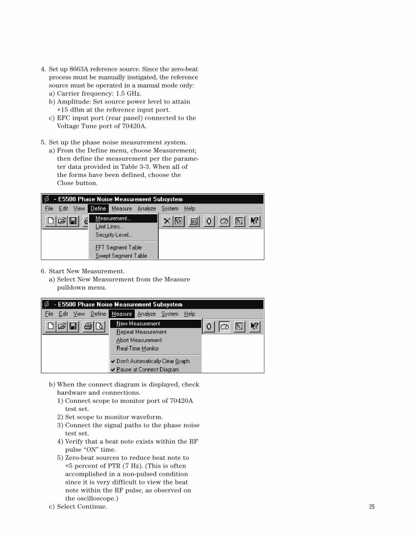
5. Set up the phase noise measurement system.
a) From the Define menu, choose Measurement;
then define the measurement per the parame-
ter data provided in Table 3-3. When all of
the forms have been defined, choose the
Close button.
6. Start New Measurement.
a) Select New Measurement from the Measure
pulldown menu.
b) When the connect diagram is displayed, check
hardware and connections.
1) Connect scope to monitor port of 70420A
test set.
2) Set scope to monitor waveform.
3) Connect the signal paths to the phase noise
test set.
4) Verify that a beat note exists within the RF
pulse “ON” time.
5) Zero-beat sources to reduce beat note to
<5 percent of PTR (7 Hz). (This is often
accomplished in a non-pulsed condition
since it is very difficult to view the beat
note within the RF pulse, as observed on
the oscilloscope.)
c) Select Continue.
26
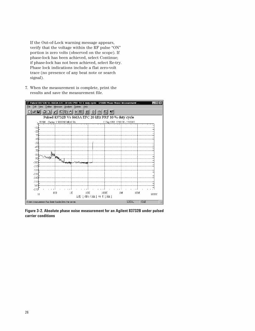
If the Out-of-Lock warning message appears,
verify that the voltage within the RF pulse “ON”
portion is zero volts (observed on the scope). If
phase-lock has been achieved, select Continue;
if phase-lock has not been achieved, select Re-try.
Phase lock indications include a flat zero-volt
trace (no presence of any beat note or search
signal).
7. When the measurement is complete, print the
results and save the measurement file.
Figure 3-2. Absolute phase noise measurement for an Agilent 83732B under pulsedcarrier conditions
27
Table 3-3. Parameter Data for Pulsed Carrier Absolute Phase Noise Measurement
Step Parameters Data
1 Type and Range TabMeasurement Type Absolute Phase Noise (using a phase-locked loop)
Couple Graph Type Checked
Start Offset Frequency 10 Hz
Stop Offset Frequency 20E+3
FFT Minimum Number of Averages 4
FFT Quality Normal
Swept Quality Fast
2 Sources TabCarrier Source Frequency 1.5E+9 Hz
Carrier Source Power 7
Power 7
Detector Input Frequency 1.5E+9 Hz
Reference Source Power 16 dBm
Detector Input Freq =
Ref Freq multiplied by 1/1
Nominal Tune Constant 15 Hz/V
Tune Range 10
Center Voltage 0
Input Resistance 600 ohms
3 Cal TabPhase Detector Constant Measure phase detector constant
VCO Tune Constant Calculate from expected
Verify calculated phase-locked
loop suppression Not Checked
Always Show Suppression Graph Not Checked
4 Block Diagram TabCarrier Source Manual
Downconverter None Selected
Reference Source Manual
Phase Detector Test Set RF Phase Detector
Test Set Tune Voltage Destination Reference Source
VCO Tune Mode EFC
5 Test Set TabInput Attenuation (Option 001 only) Set to provide appropriate power level to phase detector
LNA Low-Pass Filter 20 kHz
Auto Not Checked
DC Block Not Checked
LNA Gain Auto Gain Selected
Ignore Out-of-Lock Conditions Checked
Pulsed Carrier Checked
PLL Integration Attenuation 0 dB
6 Graph TabTitle Pulsed 83732B vs 8663A EFC 20 kHz PRF 10% Duty Cycle
Graph Type Single-Sideband Phase Noise (dBc/Hz)
X Scale Minimum 10
X Scale Maximum 100 E+6
Y Scale Maximum 0
Y Scale Minimum –170
Normalize Trace Data 1
Scale Trace Data 1
Shift Trace Data 0
Trace Smoothing Amount 0
Power Present At Input of DUT 0
28
Using a microwave downconverterFor carrier frequencies in the microwave range,
the Agilent 70421A, 70422A, and 70427A microwave
downconverters are available to downconvert a
pulsed carrier to the RF frequency range, making
it much easier to perform pulsed absolute phase
noise measurements. In this configuration, the
microwave downconverter is used to establish
a measurement PLL.
Example 2: Absolute pulsed measurement using a microwave downconverter—Agilent 8644B versus 83732B 1. Connect the components as shown in Figure 3-3.
Do not connect the signal paths to the phase
noise measurement system at this step.
2. Set up DUT (83732B).
a) Carrier frequency: 1.5 GHz
b) Amplitude: Set source power level to attain
>10 dBm at the 70420A signal input port
when using an 70420A Opt. 001, or at the
downconverter input port if using an 70420A
standard or Option 201.
c) External Pulse Enable
3. Set up pulse generator.
a) Duty Cycle = 10%
b) PRF = 20 kHz
c) Amplitude = TTL level
4. Set up 8644B reference source. Since the zero-
beat process must be manually instigated, the
reference source must be operated in a manual
mode only:
a) Carrier frequency:
300 MHz (if using an 70421A or 70422A
downconverter)
900 MHz (if using an 70427A downconverter)
b) Amplitude: Set source power level for +15 dBm
at the reference input port.
Figure 3-3. Pulsed carrier absolute phase noise measurements using a microwavedownconverter
PulseGenerator
External PulseInput
Input
E55008644B
Input
PulseModulator
ReferenceInput
Tune VoltsOut
PLL
ReferenceSource
MicrowaveDownconverter
Tune VoltsIN
Source"DUT"
PulseModulator
83732B
29
5. Set up the phase noise measurement system.
a) From the Define menu, choose Measurement;
then define the measurement per the parame-
ter data provided in Table 3-4. When all of
the forms have been defined, choose the
Close button.
b) For this configuration, the 10-MHz reference
oscillator within the down converter will be
tuned to achieve measurement phase-lock.
The internal PLL loops of the downconverter
restrict the acceptable closed-loop measure-
ment bandwidth to <<126 Hz. With an open-
loop PTR of 75 Hz, this narrow closed-loop
bandwidth is achieved by selecting 12 dB of
PLL integrator attenuation (located on Test
Set definition page).
6. Start New Measurement.
a) Select New Measurement from the Measure
pulldown menu.
b) When the connect diagram is displayed, check
hardware and connections.
1) Connect scope to monitor port of 70420A
test set.
2) Set scope to monitor waveform.
3) Connect the signal paths to the phase noise
test set.
4) Verify that a beat note exists within the RF
pulse “ON” time.
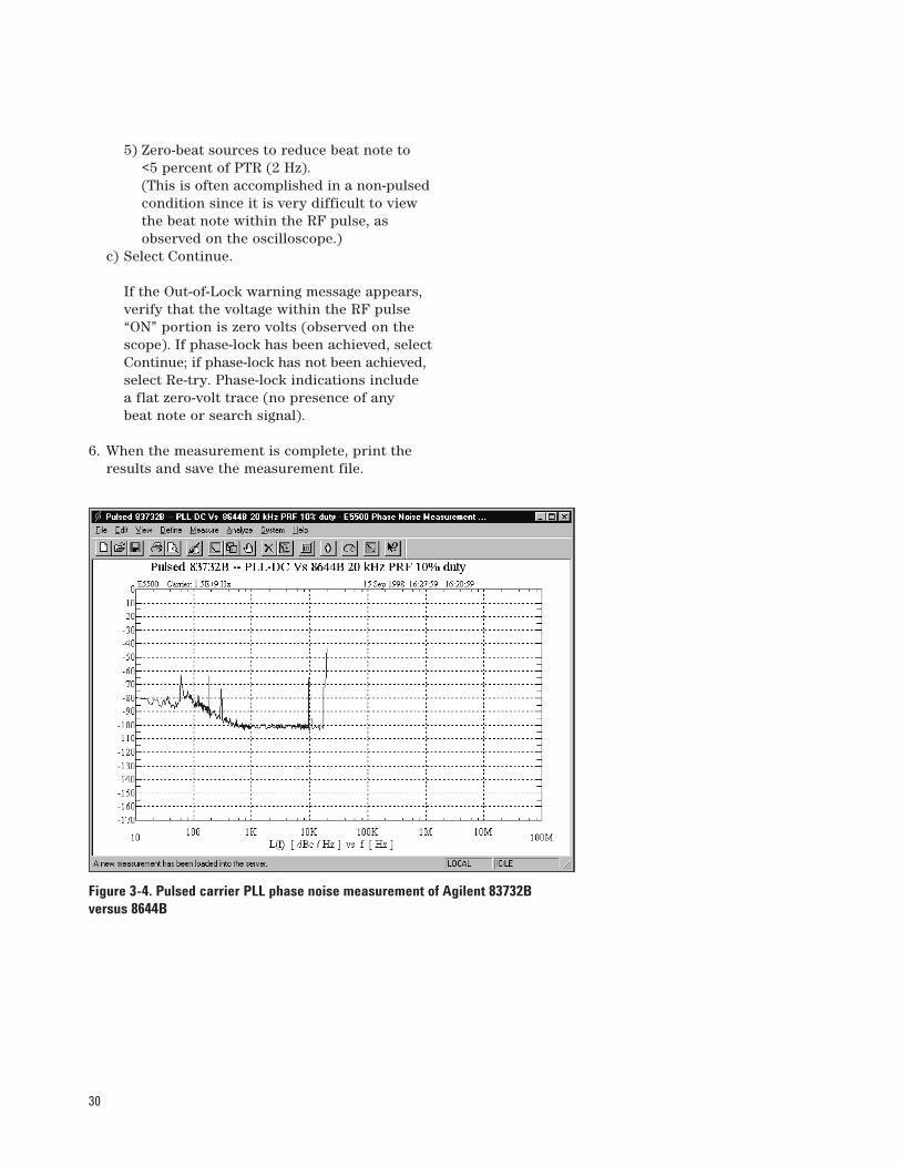
30
5) Zero-beat sources to reduce beat note to
<5 percent of PTR (2 Hz).
(This is often accomplished in a non-pulsed
condition since it is very difficult to view
the beat note within the RF pulse, as
observed on the oscilloscope.)
c) Select Continue.
If the Out-of-Lock warning message appears,
verify that the voltage within the RF pulse
“ON” portion is zero volts (observed on the
scope). If phase-lock has been achieved, select
Continue; if phase-lock has not been achieved,
select Re-try. Phase-lock indications include
a flat zero-volt trace (no presence of any
beat note or search signal).
6. When the measurement is complete, print the
results and save the measurement file.
Figure 3-4. Pulsed carrier PLL phase noise measurement of Agilent 83732Bversus 8644B
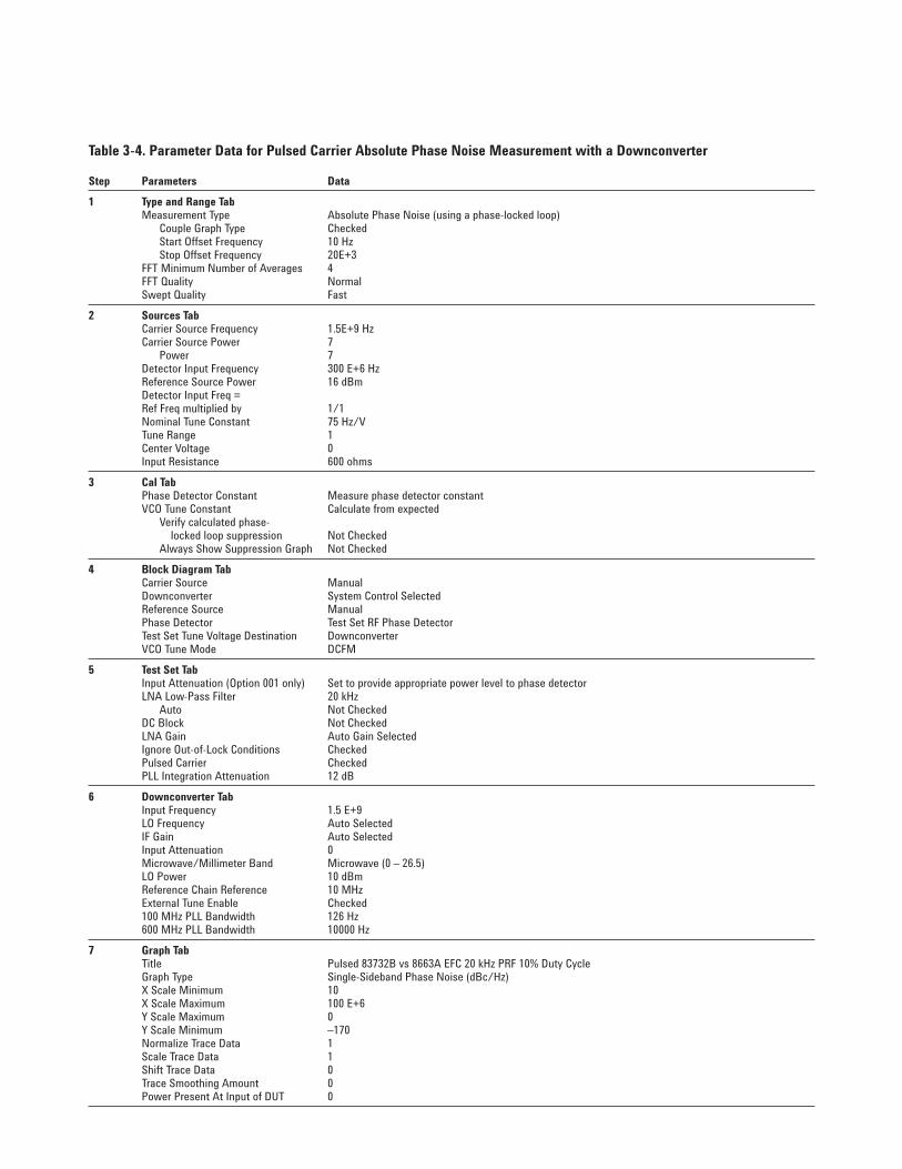
Table 3-4. Parameter Data for Pulsed Carrier Absolute Phase Noise Measurement with a Downconverter
Step Parameters Data
1 Type and Range TabMeasurement Type Absolute Phase Noise (using a phase-locked loop)
Couple Graph Type Checked
Start Offset Frequency 10 Hz
Stop Offset Frequency 20E+3
FFT Minimum Number of Averages 4
FFT Quality Normal
Swept Quality Fast
2 Sources TabCarrier Source Frequency 1.5E+9 Hz
Carrier Source Power 7
Power 7
Detector Input Frequency 300 E+6 Hz
Reference Source Power 16 dBm
Detector Input Freq =
Ref Freq multiplied by 1/1
Nominal Tune Constant 75 Hz/V
Tune Range 1
Center Voltage 0
Input Resistance 600 ohms
3 Cal TabPhase Detector Constant Measure phase detector constant
VCO Tune Constant Calculate from expected
Verify calculated phase-
locked loop suppression Not Checked
Always Show Suppression Graph Not Checked
4 Block Diagram TabCarrier Source Manual
Downconverter System Control Selected
Reference Source Manual
Phase Detector Test Set RF Phase Detector
Test Set Tune Voltage Destination Downconverter
VCO Tune Mode DCFM
5 Test Set TabInput Attenuation (Option 001 only) Set to provide appropriate power level to phase detector
LNA Low-Pass Filter 20 kHz
Auto Not Checked
DC Block Not Checked
LNA Gain Auto Gain Selected
Ignore Out-of-Lock Conditions Checked
Pulsed Carrier Checked
PLL Integration Attenuation 12 dB
6 Downconverter TabInput Frequency 1.5 E+9
LO Frequency Auto Selected
IF Gain Auto Selected
Input Attenuation 0
Microwave/Millimeter Band Microwave (0 – 26.5)
LO Power 10 dBm
Reference Chain Reference 10 MHz
External Tune Enable Checked
100 MHz PLL Bandwidth 126 Hz
600 MHz PLL Bandwidth 10000 Hz
7 Graph TabTitle Pulsed 83732B vs 8663A EFC 20 kHz PRF 10% Duty Cycle
Graph Type Single-Sideband Phase Noise (dBc/Hz)
X Scale Minimum 10
X Scale Maximum 100 E+6
Y Scale Maximum 0
Y Scale Minimum –170
Normalize Trace Data 1
Scale Trace Data 1
Shift Trace Data 0
Trace Smoothing Amount 0
Power Present At Input of DUT 0
32
This chapter includes the recommended hardware
configurations and step-by-step measurement pro-
cedures for making AM noise measurements on
pulsed carriers.
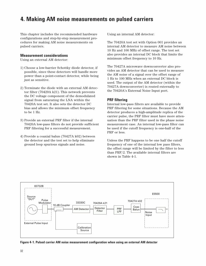
Measurement considerationsUsing an external AM detector:
1) Choose a low-barrier Schottky diode detector, if
possible, since these detectors will handle more
power than a point-contact detector, while being
just as sensitive.
2) Terminate the diode with an external AM detec-
tor filter (70429A k21). This network prevents
the DC voltage component of the demodulated
signal from saturating the LNA within the
70420A test set. It also sets the detector DC
bias and allows the minimum offset frequency
to be 1 Hz.
3) Provide an external PRF filter if the internal
70420A low-pass filters do not provide sufficient
PRF filtering for a successful measurement.
4) Provide a coaxial balun (70427A k02) between
the detector and the test set to help eliminate
ground loop spurious signals and noise.
Using an internal AM detector:
The 70420A test set with Option 001 provides an
internal AM detector to measure AM noise between
10 Hz and 100 MHz of offset range. The test set
also provides an internal DC block that limits the
minimum offset frequency to 10 Hz.
The 70427A microwave downconverter also pro-
vides an AM detector that can be used to measure
the AM noise of a signal over the offset range of
1 Hz to 100 MHz when an external DC block is
used. The output of the AM detector (within the
70427A downconverter) is routed externally to
the 70420A’s External Noise Input port.
PRF filteringInternal low-pass filters are available to provide
PRF filtering for some situations. Because the AM
detector produces a high-amplitude replica of the
carrier pulse, the PRF filter must have more atten-
uation than the PRF filter used in the phase noise
measurement case. An internal low-pass filter can
be used if the cutoff frequency is one-half of the
PRF or less.
Unless the PRF happens to be one half the cutoff
frequency of one of the internal low pass filters,
the offset range will be limited by the filter to less
than PRF/2. The available internal filters are
shown in Table 4-1.
4. Making AM noise measurements on pulsed carriers
Figure 4-1. Pulsed carrier AM noise measurement configuration when using an external AM detector
70429A k21
E5500
70427A k02
NoiseInput
RefInput
16 dB Coupler
Calibration Source
DetectorFilter
PRFLPF
CoaxBalun
33330C
Source"DUT" Pulse
Modulator
83732B
External Pulse Input
AM Detector
33
Table 4-1. Selecting an Internal Low-Pass Filter for AM Noise Measurements
PRF LNA Low-Pass Filter
≥40 kHz 20 kHz
≥400 kHz 200 kHz
≥4 MHz 2 MHz
≥40 MHz 20 MHz
However, if the PRF frequency is the same as
the low-pass filter, an external PRF filter and AM
detector may be required. PRF lines are AM in
nature and they will appear at the LNA at full
magnitude if PRF filtering does not reduce them
sufficiently.
Measurement calibration The easiest and most appropriate calibration
method for pulsed carrier AM noise measurements
is the “Single-Sided Spur Calibration Technique.”
This technique is described in the Agilent E5500
series user documentation. The method is the same
for pulsed carrier conditions as CW conditions,
with the caution that the calibration sidebands
must be <PRF/4.
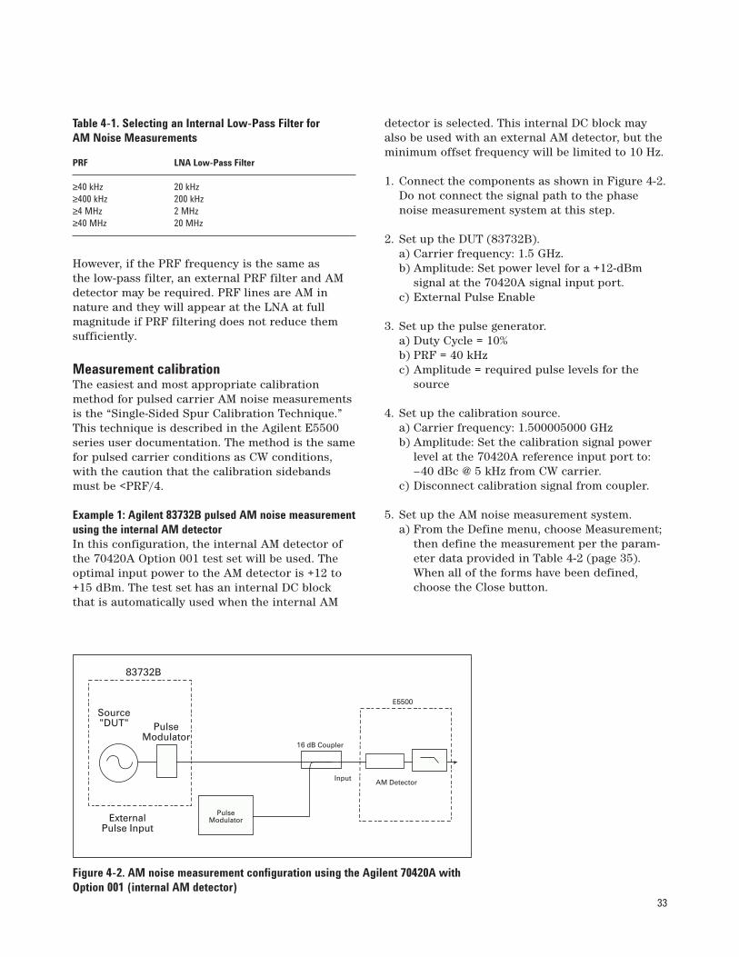
Example 1: Agilent 83732B pulsed AM noise measurementusing the internal AM detectorIn this configuration, the internal AM detector of
the 70420A Option 001 test set will be used. The
optimal input power to the AM detector is +12 to
+15 dBm. The test set has an internal DC block
that is automatically used when the internal AM
detector is selected. This internal DC block may
also be used with an external AM detector, but the
minimum offset frequency will be limited to 10 Hz.
1. Connect the components as shown in Figure 4-2.
Do not connect the signal path to the phase
noise measurement system at this step.
2. Set up the DUT (83732B).
a) Carrier frequency: 1.5 GHz.
b) Amplitude: Set power level for a +12-dBm
signal at the 70420A signal input port.
c) External Pulse Enable
3. Set up the pulse generator.
a) Duty Cycle = 10%
b) PRF = 40 kHz
c) Amplitude = required pulse levels for the
source
4. Set up the calibration source.
a) Carrier frequency: 1.500005000 GHz
b) Amplitude: Set the calibration signal power
level at the 70420A reference input port to:
–40 dBc @ 5 kHz from CW carrier.
c) Disconnect calibration signal from coupler.
5. Set up the AM noise measurement system.
a) From the Define menu, choose Measurement;
then define the measurement per the param-
eter data provided in Table 4-2 (page 35).
When all of the forms have been defined,
choose the Close button.
Figure 4-2. AM noise measurement configuration using the Agilent 70420A withOption 001 (internal AM detector)
E5500
InputAM Detector
16 dB Coupler
Source"DUT" Pulse
Modulator
83732B
ExternalPulse Input
PulseModulator
34
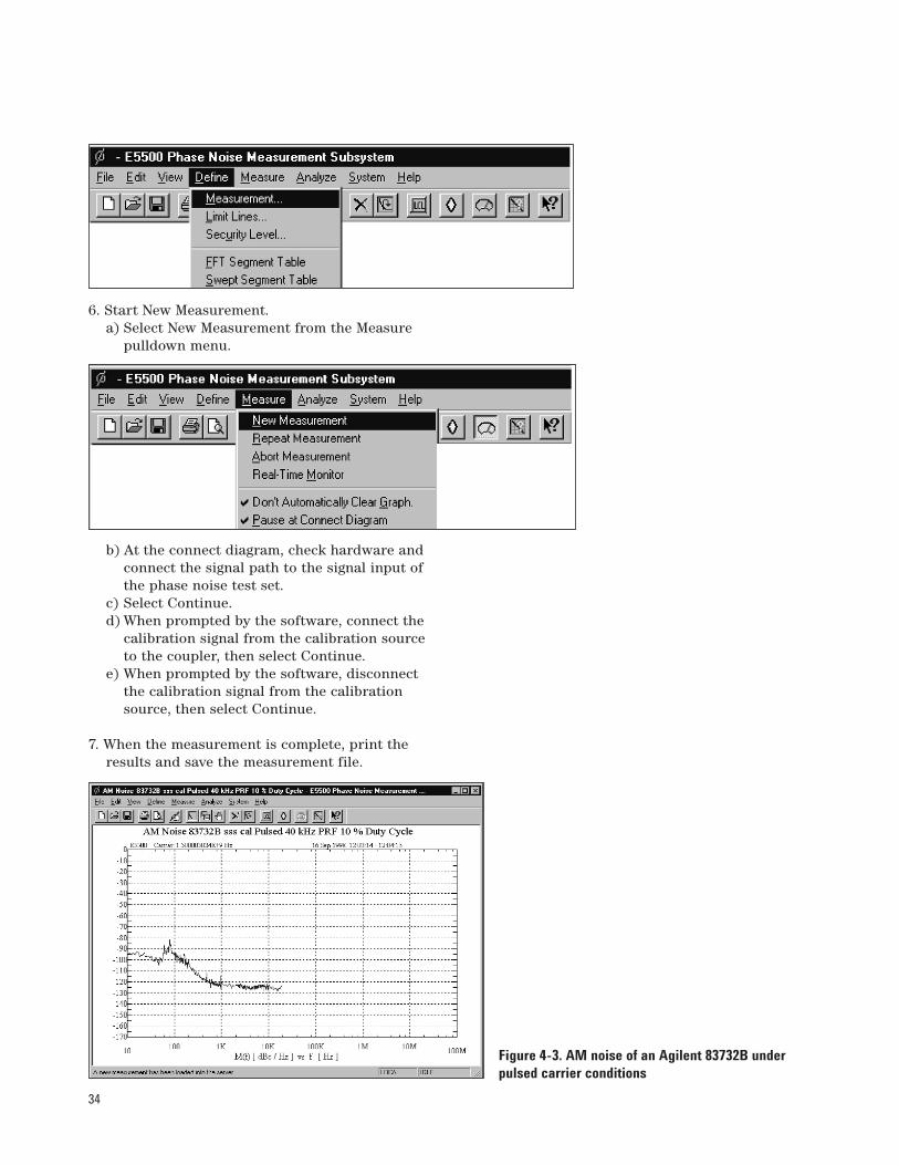
6. Start New Measurement.
a) Select New Measurement from the Measure
pulldown menu.
b) At the connect diagram, check hardware and
connect the signal path to the signal input of
the phase noise test set.
c) Select Continue.
d) When prompted by the software, connect the
calibration signal from the calibration source
to the coupler, then select Continue.
e) When prompted by the software, disconnect
the calibration signal from the calibration
source, then select Continue.
7. When the measurement is complete, print the
results and save the measurement file.
Figure 4-3. AM noise of an Agilent 83732B underpulsed carrier conditions
35
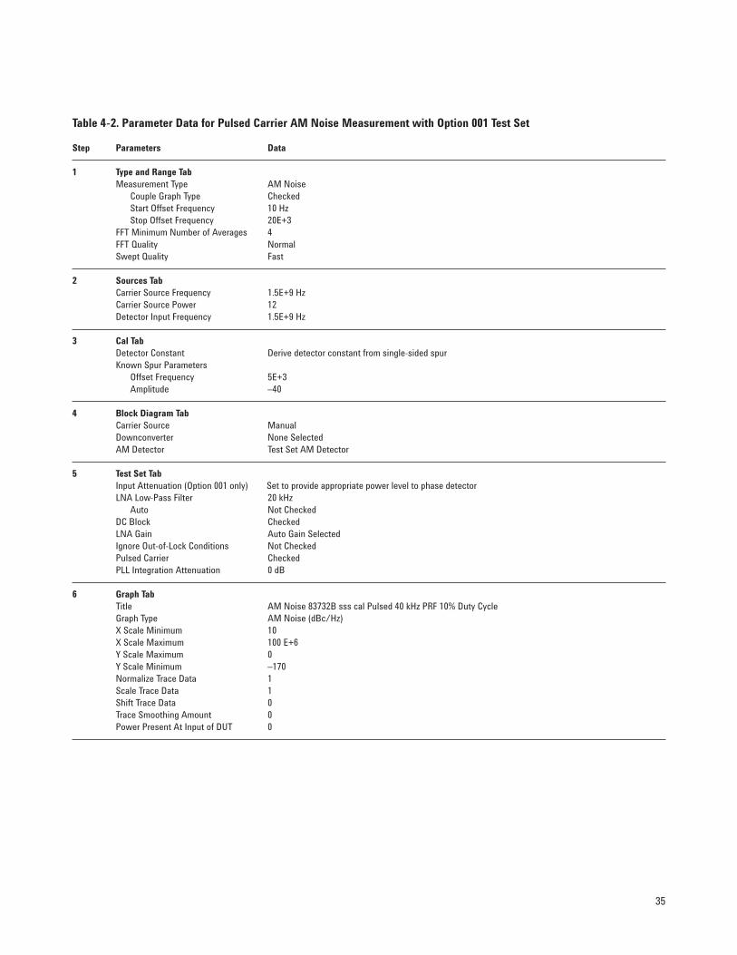
Table 4-2. Parameter Data for Pulsed Carrier AM Noise Measurement with Option 001 Test Set
Step Parameters Data
1 Type and Range TabMeasurement Type AM Noise
Couple Graph Type Checked
Start Offset Frequency 10 Hz
Stop Offset Frequency 20E+3
FFT Minimum Number of Averages 4
FFT Quality Normal
Swept Quality Fast
2 Sources TabCarrier Source Frequency 1.5E+9 Hz
Carrier Source Power 12
Detector Input Frequency 1.5E+9 Hz
3 Cal TabDetector Constant Derive detector constant from single-sided spur
Known Spur Parameters
Offset Frequency 5E+3
Amplitude –40
4 Block Diagram TabCarrier Source Manual
Downconverter None Selected
AM Detector Test Set AM Detector
5 Test Set TabInput Attenuation (Option 001 only) Set to provide appropriate power level to phase detector
LNA Low-Pass Filter 20 kHz
Auto Not Checked
DC Block Checked
LNA Gain Auto Gain Selected
Ignore Out-of-Lock Conditions Not Checked
Pulsed Carrier Checked
PLL Integration Attenuation 0 dB
6 Graph TabTitle AM Noise 83732B sss cal Pulsed 40 kHz PRF 10% Duty Cycle
Graph Type AM Noise (dBc/Hz)
X Scale Minimum 10
X Scale Maximum 100 E+6
Y Scale Maximum 0
Y Scale Minimum –170
Normalize Trace Data 1
Scale Trace Data 1
Shift Trace Data 0
Trace Smoothing Amount 0
Power Present At Input of DUT 0
Agilent Technologies’ Test and Measurement Support, Services, and AssistanceAgilent Technologies aims to maximize the value you receive,
while minimizing your risk and problems. We strive to ensure
that you get the test and measurement capabilities you paid
for and obtain the support you need. Our extensive support
resources and services can help you choose the right Agilent
products for your applications and apply them successfully.
Every instrument and system we sell has a global warranty.
Support is available for at least five years beyond the produc-
tion life of the product. Two concepts underlie Agilent’s
overall support policy: “Our Promise” and “Your Advantage.”
Our Promise“Our Promise” means your Agilent test and measurement equip-
ment will meet its advertised performance and functionality.
When you are choosing new equipment, we will help you with
product information, including realistic performance specifica-
tions and practical recommendations from experienced test
engineers. When you use Agilent equipment, we can verify that
it works properly, help with product operation, and provide
basic measurement assistance for the use of specified capabili-
ties, at no extra cost upon request. Many self-help tools are
available.
Your Advantage“Your Advantage” means that Agilent offers a wide range of
additional expert test and measurement services, which you
can purchase according to your unique technical and business
needs. Solve problems efficiently and gain a competitive edge
by contracting with us for calibration, extra-cost upgrades, out-
of-warranty repairs, and on-site education and training, as well
as design, system integration, project management, and other
professional services. Experienced Agilent engineers and tech-
nicians worldwide can help you maximize your productivity,
optimize the return on investment of your Agilent instruments
and systems, and obtain dependable measurement accuracy
for the life of those products.
By internet, phone, or fax, get assistance with all your
test and measurement needs.
Online Assistancewww.agilent.com/find/assist
Phone or FaxUnited States:
(tel) 1 800 452 4844
Canada:
(tel) 1 877 894 4414
(fax) (905) 206 4120
Europe:
(tel) (31 20) 547 2323
(fax) (31 20) 547 2390
Japan:
(tel) (81) 426 56 7832
(fax) (81) 426 56 7840
Latin America:
(tel) (305) 269 7500
(fax) (305) 269 7599
Australia:
(tel) 1 800 629 485
(fax) (61 3) 9210 5947
New Zealand:
(tel) 0 800 738 378
(fax) (64 4) 495 8950
Asia Pacific:
(tel) (852) 3197 7777
(fax) (852) 2506 9284
Product specifications and descriptions in this
document subject to change without notice.
Copyright © 1999, 2000 Agilent Technologies
Printed in U.S.A. 9/00
5968-5662E