proceedings of spie · proceedings of spie volume 6593 . proceedings of spie, 0277-786x, v. 6593...
TRANSCRIPT

PROCEEDINGS OF SPIE
SPIEDigitalLibrary.org/conference-proceedings-of-spie
Front Matter: Volume 6593
, "Front Matter: Volume 6593," Proc. SPIE 6593, Photonic Materials, Devices,and Applications II, 659301 (11 July 2007); doi: 10.1117/12.747974
Event: Microtechnologies for the New Millennium, 2007, Maspalomas, GranCanaria, Spain
Downloaded From: https://www.spiedigitallibrary.org/conference-proceedings-of-spie on 22 Mar 2020 Terms of Use: https://www.spiedigitallibrary.org/terms-of-use
PROCEEDINGS OF SPIE
Volume 6593 .
Proceedings of SPIE, 0277-786X, v. 6593
SPIE is an international society advancing an interdisciplinary approach to the science and application of light.
Photonic Materials, Devices, and Applications II
Ali Serpengüzel Gonçal Badenes Giancarlo C. Righini Editors 2–4 May 2007 Maspalomas, Gran Canaria, Spain Sponsored by SPIE Europe Cooperating Organizations PhOREMOST EOARD—The European Office of Aerospace Research and Development (United Kingdom) Sociedad Española de Óptica (Spain) Government of the Canary Islands (Spain) Universidad de las Palmas de Gran Canaria (Spain) Cátedra Telefónica, ETSI de Telecomunicación (Spain) Departamento de Ingeniería Electrónica y Automática (Spain) Instituto Universidad de Microlectrónica Aplicada (IUMA) (Spain) Published by SPIE
Downloaded From: https://www.spiedigitallibrary.org/conference-proceedings-of-spie on 22 Mar 2020Terms of Use: https://www.spiedigitallibrary.org/terms-of-use

The papers included in this volume were part of the technical conference cited on the cover and title page. Papers were selected and subject to review by the editors and conference program committee. Some conference presentations may not be available for publication. The papers published in these proceedings reflect the work and thoughts of the authors and are published herein as submitted. The publisher is not responsible for the validity of the information or for any outcomes resulting from reliance thereon. Please use the following format to cite material from this book: Author(s), "Title of Paper," in Photonic Materials, Devices, and Applications II, edited by Ali Serpengüzel, Gonçal Badenes, Giancarlo C. Righini, Proceedings of SPIE Vol. 6593 (SPIE, Bellingham, WA, 2007) Article CID Number. ISSN 0277-786X ISBN 9780819467218 Published by SPIE P.O. Box 10, Bellingham, Washington 98227-0010 USA Telephone +1 360 676 3290 (Pacific Time)· Fax +1 360 647 1445 SPIE.org Copyright © 2007, Society of Photo-Optical Instrumentation Engineers Copying of material in this book for internal or personal use, or for the internal or personal use of specific clients, beyond the fair use provisions granted by the U.S. Copyright Law is authorized by SPIE subject to payment of copying fees. The Transactional Reporting Service base fee for this volume is $18.00 per article (or portion thereof), which should be paid directly to the Copyright Clearance Center (CCC), 222 Rosewood Drive, Danvers, MA 01923. Payment may also be made electronically through CCC Online at copyright.com. Other copying for republication, resale, advertising or promotion, or any form of systematic or multiple reproduction of any material in this book is prohibited except with permission in writing from the publisher. The CCC fee code is 0277-786X/07/$18.00. Printed in the United States of America. Publication of record for individual papers is online in the SPIE Digital Library.
SPIEDigitalLibrary.org
Paper Numbering: Proceedings of SPIE follow an e-First publication model, with papers published first online and then in print and on CD-ROM. Papers are published as they are submitted and meet publication criteria. A unique, consistent, permanent citation identifier (CID) number is assigned to each article at the time of the first publication. Utilization of CIDs allows articles to be fully citable as soon they are published online, and connects the same identifier to all online, print, and electronic versions of the publication. SPIE uses a six-digit CID article numbering system in which:
The first four digits correspond to the SPIE volume number. The last two digits indicate publication order within the volume using a Base 36 numbering
system employing both numerals and letters. These two-number sets start with 00, 01, 02, 03, 04, 05, 06, 07, 08, 09, 0A, 0B … 0Z, followed by 10-1Z, 20-2Z, etc.
The CID number appears on each page of the manuscript. The complete citation is used on the first page, and an abbreviated version on subsequent pages. Numbers in the index correspond to the last two digits of the six-digit CID number.
Downloaded From: https://www.spiedigitallibrary.org/conference-proceedings-of-spie on 22 Mar 2020Terms of Use: https://www.spiedigitallibrary.org/terms-of-use
Contents
xiii Conference Committee xvii Introduction xix The nano revolution: bottom-up manufacturing with biomolecules (Plenary Paper) [6589-200] Y.-F. Li, SETI Institute (USA); J. Li, C. Paavola, NASA Ames Research Ctr. (USA); H. Kagawa,
S. L. Chan, SETI Institute (USA); J. D. Trent, NASA Ames Research Ctr. (USA) xxix Research in micro-nano-technology and systems—a European perspective. Opportunities
in Framework Programme 7: 2007–2013 (Plenary Paper) [6591-201] I. Vergara, G. Van Caenegem, F. Ibánez, European Commission (Belgium) ADVANCED OPTICAL FIBRES AND WAVEGUIDES 6593 02 Recent progress in the theory and applications of optical microfibers (Invited Paper)
[6593-25] M. Sumetsky, OFS Labs. (USA) 6593 04 Determination of the fiber birefringence induced by transversal loads by means of fiber
Bragg gratings [6593-26] S. Bette, C. Caucheteur, Faculté Polytechnique de Mons (Belgium); R. Garcia-Olcina, Univ.
Politécnica de Valencia (Spain); M. Wuilpart, Faculté Polytechnique de Mons (Belgium); S. Sales, J. Capmany, Univ. Politécnica de Valencia (Spain); P. Mégret, Faculté Polytechnique de Mons (Belgium)
6593 05 Optical switch using InP optical wire technology [6593-27] M. Lesecq, IEMN, UMR CNRS 8520, Univ. des Sciences et Technologies de Lille (France);
M. Beaugeois, Lab. de Physique de Lasers, Atomes, et Molécules, CNRS, Univ. de Sciences et Technologies de Lille (France); S. Maricot, C. Boyaval, C. Legrand, M. François, M. Muller, F. Mollot, IEMN, UMR CNRS 8520, Univ. des Sciences et Technologies de Lille (France); M. Bouazaoui, Lab. de Physique de Lasers, Atomes, et Molécules, CNRS, Univ. de Sciences et Technologies de Lille (France); J.-P. Vilcot, IEMN, UMR CNRS 8520, Univ. des Sciences et Technologies de Lille (France)
6593 06 Ultraslow optical modes in Bose-Einstein condensates [6593-48] Ö. E. Müstecaplıoglu, Koç Univ. (Turkey); D. Tarhan, Harran Univ. (Turkey) BIOPHOTONIC APPLICATIONS 6593 08 Measuring the complete spatio-temporal field of focused ultrashort laser pulses for
multi-photon microscopy [6593-91] P. Bowlan, P. Gabolde, R. Trebino, Georgia Institute of Technology (USA)
iii
Downloaded From: https://www.spiedigitallibrary.org/conference-proceedings-of-spie on 22 Mar 2020Terms of Use: https://www.spiedigitallibrary.org/terms-of-use
6593 09 Predictive analysis of thermal distribution and damage in thermotherapy on biological tissue [6593-13]
F. Fanjul-Vélez, J. L. Arce-Diego, Univ. of Cantabria (Spain) INDUSTRIAL APPLICATIONS 6593 0B High-power picosecond laser diodes based on different methods of fast gain control for
high-precision radar applications [6593-59] S. Vainshtein, J. Kostamovaara, Univ. of Oulu (Finland); V. Lantratov, N. Kaluzhniy,
S. Mintairov, A.F. Ioffe Institute (Russia) 6593 0D Fine micro-welding of thin metal sheet by high speed laser scanning [6593-61] Y. Okamoto, Okayama Univ. (Japan); A. Gillner, A. Olowinsky, J. Gedicke, Fraunhofer
Institute for Laser Technology (Germany); Y. Uno, Okayama Univ. (Japan) 6593 0E Radiation properties of two types of luminous textile devices containing plastic optical fibers
[6593-62] B. Selm, M. Rothmaier, EMPA (Switzerland) 6593 0G Current developments and applications using multi-beam laser interference lithography for
nanoscale structuring of materials [6593-81] S. Z. Su, Cardiff Univ. (United Kingdom); A. Rodríguez, S. M. Olaizola, CEIT and Tecnun, Univ.
of Navarra (Spain); C. S. Peng, C. Tan, Tampere Univ. of Technology (Finland); Y. K. Verevkin, Institute of Applied Physics (Russia); T. Berthoud, S. Tisserand, SILIOS Technologies (France)
6593 0H Nanoscale relief on quartz: from phase masks to antireflection structures [6593-82] V. N. Petryakov, A. Y. Klimov, B. A. Gribkov, Institute of Applied Physics (Russia); S. M.
Olaizola, CEIT and Tecnun, Univ. of Navarra (Spain); Y. K. Verevkin, Institute of Applied Physics (Russia)
6593 0I Formation of 4-beam laser interference patterns for nanolithography [6593-83] J. Zhang, Z. Wang, Cardiff Univ. (United Kingdom); Y. K. Verevkin, Institute of Applied Physics
(Russia); S. M. Olaizola, CEIT and Tecnun, Univ. of Navarra (Spain); C. Peng, C. Tan, Tampere Univ. of Technology (Finland); A. Rodriguez, CEIT and Tecnun, Univ. of Navarra (Spain); E. Y. Daume, Institute of Applied Physics (Russia); T. Berthou, S. Tisserand, SILIOS Technologies (France); Z. Ji, Cardiff Univ. (United Kingdom)
NANOPHOTONIC MATERIALS, DEVICES, AND APPLICATIONS 6593 0K Resonant photonic forces induced by light transmitted trough nanoapertures (Invited Paper)
[6593-19] L. A. Blanco, M. Nieto-Vesperinas, Instituto de Ciencia de Materiales de Madrid, CSIC
(Spain)
iv
Downloaded From: https://www.spiedigitallibrary.org/conference-proceedings-of-spie on 22 Mar 2020Terms of Use: https://www.spiedigitallibrary.org/terms-of-use
6593 0L Nanocomposite photonic glasses and confined structures optimizing Er3+-luminescent properties (Invited Paper) [6593-30]
C. Armellini, CNR-IFN, Institute for Photonics and Nanotechnology (Italy); A. Chiappini, Trento Univ. (Italy); A. Chiasera, M. Ferrari, Y. Jestin, CNR-IFN, Institute for Photonics and Nanotechnology (Italy); M. Mattarelli, Trento Univ. (Italy); L. Minati, ITC-IRST (Italy); M. Montagna, E. Moser, Trento Univ. (Italy); G. Nunzi Conti, Ctr. Fermi (Italy) and CNR-IFAC, N. Carrara Institute of Applied Physics (Italy); S. Pelli, CNR-IFAC, N. Carrara Institute of Applied Physics (Italy); G. C. Righini, Consiglio Nazionale delle Ricerche (Italy) and CNR-IFAC, N. Carrara Institute of Applied Physics (Italy); G. Speranza, ITC-IRST (Italy); C. Tosello, Trento Univ. (Italy)
6593 0M Stimulated emission and light amplification in Ho3+ doped oxyfluoride glasses and
glass-ceramics [6593-31] F. Lahoz, N. E. Capuj, Univ. of La Laguna (Spain); D. Navarro-Urrios, Univ. of La Laguna
(Spain) and Lab. Nanoscienze, Univ. di Trento (Italy); S. E. Hernández, Univ. of La Laguna (Spain)
6593 0N Signal enhancement in Er3+ coupled to Si nanoclusters rib-waveguides [6593-32] D. Navarro-Urrios, N. Daldosso, L. Ferraioli, Univ. di Trento (Italy); F. Gourbilleau, R. Rizk,
SIFCOM, CNRS, ENSICAEN (France); P. Pellegrino, B. Garrido, Univ. de Barcelona (Spain); L. Pavesi, Univ. di Trento (Italy)
6593 0O Rare-earth doped transparent nano-glass-ceramics: a new generation of photonic
integrated devices [6593-37] V. D. Rodríguez-Armas, Univ. de La Laguna (Spain); V. K. Tikhomirov, Nottingham Univ.
(United Kingdom); J. Méndez-Ramos, A. C. Yanes, J. Del-Castillo, Univ. de La Laguna (Spain); D. Furniss, A. B. Seddon, Nottingham Univ. (United Kingdom)
6593 0P Light emission and structural properties of undoped and erbium-doped nanostructured
silica with SnO2 nanoparticles [6593-38] S. Brovelli, Univ. College London (United Kingdom); N. Chiodini, A. Lauria, F. Meinardi,
A. Monguzzi, A. Paleari, CNISM and Univ. of Milano-Bicocca (Italy) 6593 0Q Metal nanocluster and sodalime glasses: an XPS characterization [6593-39] G. Speranza, L. Minati, FBK-IRST (Italy); A. Chiasera, M. Ferrari, CNR-IFN, Institute for Photonics
and Nanotechnology (Italy); G. C. Righini, CNR-IFAC, N. Carrara Institute Applied Physics (Italy) and CNR (Italy)
6593 0R Organic light-emitting diodes incorporating supported nanotemplates [6593-40] C.-J. Chiang, C. Rothe, M. Rosamond, A. Gallant, Durham Univ. (United Kingdom); E. Ferain,
R. Legras, Univ. catholique de Louvain (Belgium); D. Wood, A. Monkman, Durham Univ. (United Kingdom)
OPTICAL SENSORS 6593 0S Fiber optic sensors system for high-temperature monitoring of aerospace structures
[6593-52] V. Latini, Carlo Gavazzi Space (Italy); V. Striano, Istituto per la Microelettronica e
Microsistemi (Italy) and Univ. Mediterranea di Reggio Calabria (Italy); G. Coppola, I. Rendina, Istituto per la Microelettronica e Microsistemi (Italy)
v
Downloaded From: https://www.spiedigitallibrary.org/conference-proceedings-of-spie on 22 Mar 2020Terms of Use: https://www.spiedigitallibrary.org/terms-of-use
6593 0U Hydrogen sensor using fiber gratings covered by a catalytic sensitive layer [6593-54] C. Caucheteur, Faculté Polytechnique de Mons (Belgium); M. Debliquy, D. Lahem, Materia
Nova ASBL (Belgium); P. Mégret, Faculté Polytechnique de Mons (Belgium) 6593 0V Electric field measurements by a LiNbO3 probe [6593-55] L. Ciccarelli, Se.A.R.C.H. Technology (Italy); M. Medugno, I. Rendina, Consigliio Nazionale
delle Ricerche, IMM (Italy) 6593 0W An ultra-high-precision temperature sensor design based on two-port ring resonator
[6593-66] G. Rostami, Communication Technology Institute, Iran Telecommunication Research Ctr.
(Iran), Univ. of Tabriz (Iran), and Univ. of Tehran (Iran); A. Rostami, Univ. of Tabriz (Iran) 6593 0X Ultrasensitive nanomechanical photonic microsensor [6593-80] C. A. Barrios, Univ. Politécnica de Madrid (Spain) 6593 0Y Optic fiber used as sensor to measure low hydrogen concentrations [6593-84] M. Aleixandre, P. Corredera, M. L. Hernanz, J. Gutierrez-Monreal, M. J. Fernández,
M. C. Horrillo, I. Sayago, Instituto de Física Aplicada (Spain) 6593 0Z Temperature dependence of liquid crystal electrical response by impedance analysis
[6593-73] J. C. Torres, N. Gaona, I. Pérez, V. Urruchi, J. M. S. Pena, Univ. Carlos III (Spain) ORGANIC LIGHT EMITTERS 6593 10 Effect of PEDOT:PSS ratio on the electrical and optical properties of OLEDs [6593-71] M. Petrosino, Univ. of Salerno (Italy); P. Vacca, Univ. of Salerno (Italy) and Enea Portici
Research Ctr. (Italy); R. Miscioscia, G. Nenna, C. Minarini, Enea Portici Research Ctr. (Italy); A. Rubino, Univ. of Salerno (Italy)
6593 11 Effect of electrodes properties on OLED performances [6593-72] M. Petrosino, Univ. of Salerno (Italy); P. Vacca, Univ. of Salerno (Italy) and Enea Portici
Research Ctr. (Italy); R. Miscioscia, G. Nenna, C. Minarini, Enea Portici Research Ctr. (Italy); A. Rubino, Univ. of Salerno (Italy)
PHOTONIC CRYSTALS AND METAMATERIALS 6593 12 Experimental demonstration of sub-wavelength imaging by left handed metamaterials
(Invited Paper) [6593-04] E. Ozbay, Bilkent Univ. (Turkey) 6593 13 Playing with light in diatoms: small water organisms with a natural photonic crystal structure
(Invited Paper) [6593-09] L. De Stefano, CNR-IMM (Italy); M. De Stefano, Second Univ. of Naples (Italy); P. Maddalena,
Univ. of Naples Federico II (Italy); L. Moretti, Univ. Mediterranea of Reggio Calabria (Italy); I. Rea, CNR-IMM (Italy) and Univ. of Naples Federico II (Italy); V. Mocella, I. Rendina, CNR-IMM (Italy)
vi
Downloaded From: https://www.spiedigitallibrary.org/conference-proceedings-of-spie on 22 Mar 2020Terms of Use: https://www.spiedigitallibrary.org/terms-of-use

6593 14 Tunable one-dimensional photonic crystal slabs (Invited Paper) [6593-15] R. Beccherelli, B. Bellini, Istituto per la Microelettronica e Microsistemi, CNR (Italy);
D. Zografopoulos, E. Kriezis, Aristotle Univ. of Thessaloniki (Greece) 6593 15 Second harmonic superprism effect in 2D nonlinear photonic crystals [6593-03] E. Centeno, D. Felbacq, GES UMR-CNRS, Univ. Montpellier II (France) 6593 16 Negative refraction devices based on self-collimating photonic crystals [6593-05] P. Dardano, Istituto per la Microelettronica e Microsistemi, CNR (Italy) and Univ. degli Studi
di Napoli Federico II (Italy); V. Mocella, Istituto per la Microelettronica e Microsistemi, CNR (Italy); L. Moretti, Univ. Mediterranea (Italy) and Istituto per la Microelettronica e Microsistemi, CNR (Italy); I. Rendina, Istituto per la Microelettronica e Microsistemi, CNR (Italy)
6593 17 Wave propagation in self-waveguiding and negative refracting photonic crystals [6593-06] J. L. Garcia-Pomar, M. Nieto-Vesperinas, Instituto de Ciencia de Materiales de Madrid, CSIC
Cantoblanco (Spain) 6593 18 Quasi-ordered photonic bandgap materials of biologic origin: butterfly scales [6593-10] L. P. Biró, Research Institute for Technical Physics and Materials Science (Hungary); Zs. Bálint,
Hungarian Natural History Museum (Hungary); K. Kertész, Z. Vértesy, G. I. Márk, L. Tapasztó, Research Institute for Technical Physics and Materials Science (Hungary); V. Lousse, J. P. Vigneron, Facultes Univ. Notre Dame de la Paix (Belgium)
6593 19 Designing waveguides and microcavities in hybrid architectures based on direct and
inverse opals [6593-11] K. Vynck, G. Qiu, D. Cassagne, E. Centeno, UMR 5650 CNRS, Univ. Montpellier II (France) 6593 1A Aperiodic photonic bandgap devices based on nanostructured porous silicon [6593-16] I. Rea, CNR-IMM (Italy) and Univ. of Naples Frederico II (Italy); L. Moretti, Univ. Mediterranea
of Reggio Calabria (Italy); L. Rotiroti, CNR-IMM (Italy) and Univ. of Naples Frederico II (Italy); I. Rendina, L. De Stefano, CNR-IMM (Italy)
PHOTONIC SYSTEM INTEGRATION 6593 1C Embodiment of optical interconnection circuits for the mobile phone application [6593-42] J.-W. Seo, S.-M. Seo, Y.-K. Oh, D.-H. Jang, Samsung Electronics (South Korea) 6593 1D Adaptive OFDM system for multi-user communications over the indoor wireless optical
channel [6593-43] O. González, S. Rodríguez, Univ. of La Laguna (Spain); R. Pérez-Jiménez, Univ. of Las Palmas
de Gran Canaria (Spain); B. R. Mendoza, Univ. of La Laguna (Spain); F. Delgado, Univ. of Las Palmas de Gran Canaria (Spain)
RING RESONATORS IN DWDM 6593 1E Ring resonator with an internal Sagnac loop for dispersion compensation in DWDM
backbone networks [6593-33] J. Montalvo, C. Vázquez, Carlos III Univ. of Madrid (Spain)
vii
Downloaded From: https://www.spiedigitallibrary.org/conference-proceedings-of-spie on 22 Mar 2020Terms of Use: https://www.spiedigitallibrary.org/terms-of-use
6593 1F Switches and tunable filters based on ring resonators and liquid crystals [6593-34] C. Vázquez, P. Contreras, J. Montalvo, J. M. Sánchez Pena, Carlos III Univ. of Madrid (Spain);
A. d'Alessandro, D. Donisi, Univ. degli Studi di Roma La Sapienza (Italy) 6593 1G All-optical tunable dispersion compensator using ring resonator and electromagnetically
induced transparency [6593-35] G. Rostami, Univ. of Tehran (Iran) and Communication Technology Institute (Iran);
A. Rostami, Univ. of Tabriz (Iran) 6593 1H A new integrated optical high-resolution spectrum analyzer structure based on ring
resonator applicable to DWDM networks [6593-36] G. Rostami, Communication Technology Institute (Iran), Univ. of Tabriz (Iran) and Univ. of
Tehran (Iran); A. Rostami, Univ. of Tabriz (Iran); J. Rashed-Mohassel, Univ. of Tehran (Iran) SILICON PHOTONICS 6593 1I Future prospects for silicon photonics (Invited Paper) [6593-88] W. R. Headley, G. T. Reed, G. Z. Mashanovich, B. Timotijevic, F. Y. Gardes, D. Thomson,
P. Yang, Univ. of Surrey (United Kingdom); E.-J. Teo, D. J. Blackwood, M. B. H. Breese, A. A. Bettiol, National Univ. of Singapore (Singapore); P. Waugh, Univ. of Surrey (United Kingdom)
6593 1J Silicon microsphere photonics (Invited Paper) [6593-28] A. Serpengüzel, A. Kurt, U. K. Ayaz, Koç Univ. (Turkey) 6593 1K Optical study of polymer infiltration into porous Si-based structures (Invited Paper) [6593-08] S. Cheylan, Institut de Ciències Fotòniques (Spain); F. Yu. Sychev, T. Murzina, Moscow State
Univ. (Russia); T. Trifonov, Univ. Politècnica de Cataluña (Spain); A. Maydykovskiy, Moscow State Univ. (Russia); J. Puigdollers, R. Alcubilla, Univ. Politècnica de Cataluña (Spain); G. Badenes, Institut de Ciències Fotòniques (Spain)
6593 1M Photonic crystal cavities embedded in photonic wire waveguides (Invited Paper) [6593-87] A. R. Md Zain, H. M. H. Chong, M. Gnan, A. Samarelli, M. Sorel, R. M. De La Rue, Univ. of
Glasgow (United Kingdom) 6593 1N Analysis of a planar silicon opto-electronic modulator based on the waveguide-vanishing
effect [6593-29] G. Coppola, I. Mario, I. Rendina, Istituto per la Microelettronica e Microsistemi, Unità di
Napoli (Italy) 6593 1O Study of the effects on the Raman spectra of adsorption strain in porous silicon [6593-67] M. A. Ferrara, Istituto per la Microelettronica e Microsistemi, CNR (Italy) and DIMET, Univ.
Mediterranea (Italy); M. G. Donato, MECMAT, Univ. Mediterranea (Italy); L. Sirleto, Istituto per la Microelettronica e Microsistemi, CNR (Italy); G. Messina, S. Santangelo, MECMAT, Univ. Mediterranea (Italy); L. Rotiroti, I. Rendina, Istituto per la Microelettronica e Microsistemi, CNR (Italy)
6593 1P The role of the temperature and aging in the photoluminescence behaviour on porous
silicon stain etched films [6593-70] B. González-Díaz, J. Méndez-Ramos, J. del-Castillo, B. Díaz-Herrera, R. Guerrero-Lemus,
C. Hernandez-Rodriguez, V. D. Rodríguez, Univ. de La Laguna (Spain)
viii
Downloaded From: https://www.spiedigitallibrary.org/conference-proceedings-of-spie on 22 Mar 2020Terms of Use: https://www.spiedigitallibrary.org/terms-of-use
6593 1Q Post-etching shaping of macroporous silicon [6593-76] T. Trifonov, M. Garín, A. Rodríguez, P. Ortega, Univ. Politècnica de Catalunya (Spain);
L. F. Marsal, Univ. Rovira i Virgili (Spain); R. Alcubilla, Univ. Politècnica de Catalunya (Spain) TELECOMMUNICATION DEVICES, SYSTEMS, AND APPLICATIONS 6593 1S Dynamic control of noisy quantum memory channels (Invited Paper) [6593-47] G. Gordon, G. Kurizki, Weizmann Institute of Science (Israel) 6593 1U High-performance InAs quantum-dot infrared photodetectors grown on InP substrate
operating at room temperature and high operating temperature focal plane array (Invited Paper) [6593-44]
S. Tsao, H. Lim, W. Zhang, M. Razeghi, Northwestern Univ. (USA) 6593 1V High-power mid- and far-wavelength infrared lasers for free space communication
(Invited Paper) [6593-56] M. Razeghi, A. Evans, J. Nguyen, Y. Bai, S. Slivken, S. R. Darvish, K. Mi, Northwestern Univ.
(USA) 6593 1W Gain compression and recovery in semiconductor optical amplifiers (Invited Paper)
[6593-49] M. J. Adams, Univ. of Essex (United Kingdom) 6593 1X Self-referencing techniques in photonics sensors and multiplexing (Invited Paper) [6593-63] C. Vázquez, J. Montalvo, D. S. Montero, P. C. Lallana, Carlos III Univ. of Madrid (Spain) 6593 1Z Characterization of an optically enhanced conventional 10 GHz receiver for RZ systems
over 100 GHz [6593-46] M. Scaffardi, F. Fresi, Scuola Superiore Sant' Anna, CEIRC (Italy); P. Ghelfi, CNIT (Italy);
M. Secondini, Scuola Superiore Sant' Anna, CEIRC (Italy); A. Bogoni, L. Poti, CNIT (Italy) 6593 20 Reflective optical bistability and nonlinear switching in a 1550-nm vertical-cavity
semiconductor optical amplifier (VCSOA) [6593-50] A. Hurtado, I. D. Henning, M. J. Adams, Univ. of Essex (United Kingdom) 6593 21 Optical gain in dye-doped polymer waveguides using oxidized porous silicon cladding
[6593-51] D. Navarro-Urrios, M. Ghulinyan, P. Bettotti, Univ. of Trento (Italy); N. Capuj, Univ. of La
Laguna (Spain); C. J. Oton, Univ. of Southampton (United Kingdom); F. Lahoz, I. R. Martin, Univ. of La Laguna (Spain); L. Pavesi, Univ. of Trento (Italy)
6593 22 Continuous-wave operation of photonic band-edge laser at 1.55 µm on silicon wafer
[6593-57] G. Vecchi, F. Raineri, I. Sagnes, A. M. Yacomotti, P. Monnier, R. Braive, S. Bouchoule,
A. Levenson, R. Raj, Lab. de Photonique et de Nanostructures, CNRS (France) 6593 23 Linewidth influence in photonics logic device [6593-58] A. P. Gonzalez-Marcos, T. Vivero, J. A. Martín-Pereda, Univ. Politécnica de Madrid (Spain) 6593 24 Near-UV InGaN/GaN-based dual-operation quantum optoelectronic devices [6593-64] T. Ozel, E. Sari, S. Nizamoglu, H. V. Demir, Bilkent Univ. (Turkey)
ix
Downloaded From: https://www.spiedigitallibrary.org/conference-proceedings-of-spie on 22 Mar 2020Terms of Use: https://www.spiedigitallibrary.org/terms-of-use
6593 25 Monolithic fully integrated programmable micro-diffraction grating based on electro- optical materials [6593-65]
G. G. Bentini, CNR, Istituto per la Microelettronica e Microsistemi (Italy); A. Parini, Univ. degli Studi di Ferrara (Italy); M. Chiarini, Carlo Gavazzi Space S.p.A. (Italy); M. Bianconi, A. Cerutti, A. Nubile, S. Sugliani, CNR, Istituto per la Microelettronica e Microsistemi (Italy); G. Pennestrì, Carlo Gavazzi Space S.p.A (Italy); G. Bellanca, S. Trillo, Univ. degli Studi di Ferrara (Italy); S. Petrini, M. Gallerani, P. De Nicola, F. Bergamini, CNR, Istituto per la Microelettronica e Microsistemi (Italy)
6593 26 Analysis of measurement uncertainty in THz-TDS [6593-68] W. Withayachumnankul, H. Lin, S. P. Mickan, B. M. Fischer, D. Abbott, The Univ. of Adelaide
(Australia) 6593 27 Conceptual design of an inexpensive POF demultiplexer [6593-74] M. Haupt, U. H. P. Fischer, Harz Univ. of Applied Studies and Research (Germany); H. Kragl,
Harz Univ. of Applied Studies and Research (Germany) and DieMount GmbH (Germany) 6593 28 Study of optical microcavities with electromagnetically induced transparency for
developing new photonic devices [6593-75] J. L. Arce-Diego, F. Fanjul-Vélez, D. Pereda-Cubián, N. Ortega-Quijano, Cantabria Univ.
(Spain) 6593 29 Performances of RCE photodetectors based on the internal photoemission effect [6593-77] M. Casalino, Univ. degli Studi Mediterranea di Reggio Calabria (Italy) and Isituto per la
Microelettronica e Microsistemi, CNR (Italy); L. Sirleto, Isituto per la Microelettronica e Microsistemi, CNR (Italy); L. Moretti, F. Della Corte, Univ. degli Studi Mediterranea di Reggio Calabria (Italy); I. Rendina, Isituto per la Microelettronica e Microsistemi, CNR (Italy)
6593 2B Efficient light-emitting microstructures induced by EUV radiation in thermally evaporated
lithium fluoride thin films [6593-85] R. M. Montereali, S. Almaviva, F. Bonfigli, ENEA (Italy); A. Faenov, Institute for High Energy
Densities of Joint Institute for High Temperatures (Russia); F. Flora, I. Franzini, E. Nichelatti, ENEA (Italy); T. Pikuz, Institute for High Energy Densities of Joint Institute for High Temperatures (Russia); M. A. Vincenti, G. Baldacchini, ENEA (Italy)
6593 2C A single photon avalanche detector (SPAD) [6593-90] S. Tudisco, INFN, Lab. Nazionali del Sud (Italy); S. Privitera, F. Musumeci, L. Lanzanò,
A. Scordino, INFN, Lab. Nazionali del Sud (Italy) and DMFCI, Univ. di Catania (Italy); A. Campisi, L. Cosentino, G. Condorelli, P. Finocchiaro, INFN, Lab. Nazionali del Sud (Italy); S. Lombardo, M. Mazzillo, E. Sciacca, ST-Microelectronics & IMM-CNR (Italy)
WHISPERING GALLERY MODE RESONATORS 6593 2E Strong coupling of single quantum dots to micropillars (Invited Paper) [6593-21] S. Götzinger, Stanford Univ. (USA) and ETH Zürich (Switzerland); D. Press, Stanford Univ. (USA);
S. Reitzenstein, K. Hofmann, A. Löffler, M. Kamp, A. Forchel, Univ. Würzburg (Germany); Y. Yamamoto, Stanford Univ. (USA)
x
Downloaded From: https://www.spiedigitallibrary.org/conference-proceedings-of-spie on 22 Mar 2020Terms of Use: https://www.spiedigitallibrary.org/terms-of-use

6593 2G Amplified spontaneous emission from a microtube cavity with whispering gallery modes [6593-23]
Y. P. Rakovich, S. Balakrishnan, Y. Gun’ko, T. S. Perova, A. Moore, J. F. Donegan, Trinity College Dublin (Ireland)
6593 2H The operating characteristics of an optical near-field generator fabricated on laser diodes
[6593-24] M. Fukuda, Y. Yamasaki, A. Oguma, A. Utsumi, N. Oota, Toyohashi Univ. of Technology
(Japan) Author Index
xi
Downloaded From: https://www.spiedigitallibrary.org/conference-proceedings-of-spie on 22 Mar 2020Terms of Use: https://www.spiedigitallibrary.org/terms-of-use

Downloaded From: https://www.spiedigitallibrary.org/conference-proceedings-of-spie on 22 Mar 2020Terms of Use: https://www.spiedigitallibrary.org/terms-of-use
Conference Committee
Symposium Chairs
José Fco. López, Universidad de Las Palmas de Gran Canaria (Spain) Roberto Sarmiento Rodríguez, Universidad de Las Palmas de Gran
Canaria (Spain) Steve Kang, University of California, Santa Cruz (USA)
Conference Chairs
Ali Serpengüzel, Koç University (Turkey) Gonçal Badenes, Institut de Ciències Fotòniques (Spain) Giancarlo C. Righini, Istituto di Fisica Applicata Nello Carrara (Italy)
Program Committee
Michael J. Adams, University of Essex (United Kingdom) Roel G. Baets, Universiteit Gent (Belgium) Pascal A. Baldi, Université de Nice Sophia Antipolis (France) Richard K. Chang, Yale University (USA) Brian Culshaw, University of Strathclyde (United Kingdom) Nadir Dagli, University of California, Santa Barbara (USA) Richard M. De La Rue, University of Glasgow (United Kingdom) G. di Bartolo, LNS (Italy) Robert E. Fischer, OPTICS 1, Inc. (USA) F. Javier Garcia de Abajo, Consejo Superior de Investigaciones
Científicas (Spain) Fenna D. Hanes, New England Board of Higher Education (USA) M. Saif Islam, University of California, Davis (USA) Gershon Kurizki, Weizmann Institute of Science (Israel) El-Hang Lee, Inha University (South Korea) Eric Mazur, Harvard University (USA) Anna G. Mignani, Istituto di Fisica Applicata Nello Carrara (Italy) Manuel Nieto-Vesperinas, Consejo Superior de Investigaciones
Científicas (Spain) Ekmel Özbay, Bilkent University (Turkey) Roberto R. Panepucci, Florida International University (USA) Lorenzo Pavesi, Università degli Studi di Trento (Italy) Valerio Pruneri, Avanex, Inc. (Italy) Henri J. Rajbenbach, European Commission (Belgium) Manijeh Razeghi, Northwestern University (USA) Ivo Rendina, Istituto per la Microelettronica e Microsistemi (Italy) PierMario Repetto, Centro Ricerche Fiat (Italy)
xiii
Downloaded From: https://www.spiedigitallibrary.org/conference-proceedings-of-spie on 22 Mar 2020Terms of Use: https://www.spiedigitallibrary.org/terms-of-use
Vahid Sandoghdar, ETH Zürich (Switzerland) Costas M. Soukoulis, Iowa State University (USA) Hugo Thienpont, Vrije Universiteit Brussel (Belgium) M. S. Unlu, Boston University (USA) Niek F. van Hulst, Institut de Ciències Fotòniques (Spain) Claude Weisbuch, Ecole Polytechnique (France)
Session Chairs
Advanced Optical Fibres and Waveguides Gonçal Badenes, Institut de Ciències Fotòniques (Spain)
Biophotonic Applications Giancarlo C. Righini, Istituto di Fisica Applicata Nello Carrara (Italy)
Industrial Applications Alexander Heisterkamp, Laser Zentrum Hannover e.V. (Germany)
Nanophotonic Materials, Devices, and Applications Lorenzo Pavesi, Università degli Studi di Trento (Italy) Niek F. van Hulst, Institut de Ciències Fotòniques (Spain) Manuel Nieto-Vesperinas, Consejo Superior de Investigaciones
Científicas (Spain)
Optical Sensors Gershon Kurizki, Weizmann Institute of Science (Israel)
Photonic Crystals and Metamaterials Gonçal Badenes, Institut de Ciències Fotòniques (Spain) Ekmel Özbay, Bilkent University (Turkey) Giancarlo C. Righini, Istituto di Fisica Applicata Nello Carrara (Italy) Ivo Rendina, Consiglio Nazionale delle Ricerche (Italy)
Photonic System Integration Ali Serpengüzel, Koç University (Turkey)
Ring Resonators in DWDM Stephan J. Goetzinger, Stanford University (USA)
Silicon Photonics Giancarlo C. Righini, Istituto di Fisica Applicata Nello Carrara (Italy) Maurizio Ferrari, Università degli Studi di Trento (Italy) Patrice Féron, École Nationale Supérieure des Sciences Appliquées et
de Technologie (France)
xiv
Downloaded From: https://www.spiedigitallibrary.org/conference-proceedings-of-spie on 22 Mar 2020Terms of Use: https://www.spiedigitallibrary.org/terms-of-use

Telecommunication Devices, Systems, and Applications El-Hang Lee, Inha University (South Korea) Carmen Vázquez García, Universidad Carlos III de Madrid (Spain) Michael J. Adams, University of Essex (United Kingdom) Manijeh Razeghi, Northwestern University (USA) Louay A. Eldada, DuPont Photonics Technologies (USA)
Whispering Gallery Mode Resonators Romeo Beccherelli, Consiglio Nazionale delle Ricerche (Italy) Oliver Benson, Humboldt-Universität zu Berlin (Germany)
xv
Downloaded From: https://www.spiedigitallibrary.org/conference-proceedings-of-spie on 22 Mar 2020Terms of Use: https://www.spiedigitallibrary.org/terms-of-use

Downloaded From: https://www.spiedigitallibrary.org/conference-proceedings-of-spie on 22 Mar 2020Terms of Use: https://www.spiedigitallibrary.org/terms-of-use

Introduction Photonics science and technology is having a tremendous impact on our global society at the beginning of this millennium and this first century will probably be called the “photonic century,” as the last century of the last millennium was called the “electronic century.” This rapid development is not only occurring in the telecommunications field but also spans a wide range of additional applications that include sensing, storage, and displays. Recent advances in the development of new photonic materials, devices, components, systems, and techniques, especially those related to microtechnology and nanoscience, suggest that these photonics related areas will play an even increasingly important role in the near future. The scope of this conference on photonics materials, devices, and applications has been to bring together the optical research scientists and photonics engineers, who work on the different aspects of this fascinating field of science and technology, and thus to provide an interdisciplinary update and review of innovations in photonic materials, devices and systems, microtechnology and nanotechnology advances, as well as theoretical, experimental, and numerical tools that support these innovations. The conference included the topics such as advanced optical fibres and waveguides, biophotonic applications, industrial applications, nanophotonic materials, devices, and applications, optical sensors, organic light emitters, photonic crystals and metamaterials, photonic system integration, ring resonators in DWDM, silicon photonics, telecommunication devices, systems, and applications, and whispering gallery mode resonators. Nanophotonics is enabling single photon and single molecule control. Silicon photonics and photonic system integration fields are experiencing a rapid growth with novel device and components. Biophotonics is becoming an ever growing field with new diagnostic and therapy techniques. Organic devices are catching up with inorganic devices. Metamaterials herald the possibility of optical cloaking. We are certainly experiencing very exciting times. Although this volume includes a fraction of the global research and development effort in the vast field of photonics, we hope that these papers by world renowned experts in the field of photonics bring the reader up to date with state-of-the-art photonics technology and science.
Ali Serpengüzel Gonçal Badenes
Giancarlo C. Righini
xvii
Downloaded From: https://www.spiedigitallibrary.org/conference-proceedings-of-spie on 22 Mar 2020Terms of Use: https://www.spiedigitallibrary.org/terms-of-use

Downloaded From: https://www.spiedigitallibrary.org/conference-proceedings-of-spie on 22 Mar 2020Terms of Use: https://www.spiedigitallibrary.org/terms-of-use

The Nano Revolution: Bottom-up Manufacturing with Biomolecules
Yi-Fen Lia, Jing Lib, Chad Paavolab, Hiromi Kagawaa, Suzanne L. Chana, Jonathan D. Trent*b
aSETI Institute, 515 N. Whisman Road, Mountain View, CA USA 94043; bNASA Ames Research Center, Bioengineering Branch, Mail Stop 239-15, Moffett Field, CA USA
94035
ABSTRACT
As the nano-scale becomes a focus for engineering electronic, photonic, medical, and other important devices, an unprecedented role for biomolecules is emerging to address one of the most formidable problems in nano-manufacturing: precise manipulation and organization of matter on the nano-scale. Biomolecules are a solution to this problem because they themselves are nanoscale particles with intrinsic properties that allow them to precisely self-assemble and self-organize into the amazing diversity of structures observed in nature. Indeed, there is ample evidence that the combination of molecular recognition and self-assembly combined with mutation, selection, and replication have the potential to create structures that could truly revolutionize manufacturing processes in many sectors of industry. Genetically engineered biomolecules are already being used to make the next generation of nano-scale templates, nano-detailed masks, and molecular scaffolds for the future manufacturing of electronic devices, medical diagnostic tools, and chemical engineering interfaces. Here we present an example of this type of technology by showing how a protein can be genetically modified to form a new structure and coated with metal to lead the way to producing “nano-wires,” which may ultimately become the basis for self-assembled circuitry.
Keywords: Nanotechnology, biomolecule, chaperonin, self-assembly, nanowire
1. INTRODUCTION The controlled organization of materials on the nanoscale is the ultimate goal of the bottom-up manufacturing pursued by nanotechnology. At this scale, material packing densities and manipulations present technical challenges for current patterning manufacturing technologies, such as dip-pen and electron and ion beams lithography. While this scale exceeds the limits of most lithographic patterning processes, packing densities and quantum effects (e.g., single electron tunneling quantum confinement) are strong incentives to pursue this miniaturization process to nanometer size scales. The alternative approach that is widely being pursued involves self-assembly and self-organization.
Self-assembled inorganic and organic molecules that naturally form one-, two- and three- dimensional structures are a major focus of research in nanotechnology. One- and two-dimensional nano-structured materials are being investigated for their use as templates, scaffolds, or guides for fabricating prototype devices, such as quantum-dot lasers (1), single-electron transistors (2), memory units (3), sensors (4), optical detectors (5), and light-emitting diodes (LEDs) (6). There is currently also a growing interest in fabricating one-dimensional (1D) nanostructures from metal or semi-conducting materials, which can be used as both interconnects and functional units in electronic, electrochemical, and electromechanical nano-devices (7). Efforts to fabricate such nano-wires and nano-tubes include using inorganic templates, which take advantage of step edges of solid substrates, and organic templates, which take advantage of self-assembling polymers, including synthetic polymers and biological macromolecules, including DNA and proteins.
Biomolecules in general and proteins in particular, are not only capable of self-assembling into intricate patterns with nanoscale architecture, they can be manipulated and functionalized using methods developed for biotechnology. The astonishing diversity of structures formed by proteins is apparent in nature. Because their synthesis is genetically directed, both their structure and their function can be effectively manipulated. DNA and various proteins have already been used as templates for nanowires and nanotubes that have been incorporated into nano-structured materials and devices (8-14). We are exploring potential nanotechnology applications for a class of 60 kDa proteins, known as Hsp60s.
Plenary Paper
Smart Sensors, Actuators, and MEMS III, edited by Thomas Becker, Carles Cané, N. Scott Barker, Proc. of SPIE Vol. 6589, 658902, (2007) · 0277-786X/07/$18 · doi: 10.1117/12.740793
Proc. of SPIE Vol. 6589 658902-1
xix
Downloaded From: https://www.spiedigitallibrary.org/conference-proceedings-of-spie on 22 Mar 2020Terms of Use: https://www.spiedigitallibrary.org/terms-of-use
1.1 Obtaining the protein building blocks
The HSP60s are proteins that in the presence of ATP/Mg self-assemble into regular double-ring structures known as “chaperonins.” In nature, chaperonins are ubiquitous and essential biological structures comprised of 14-, 16-, or 18-HSP60 subunits arranged as two stacked rings forming supramolecular structures 16 to 18 nm high and 15 to 17 nm wide, depending on their species of origin. The HSP60-subunits consist of three structural domains named in accordance with their position in the double ring. The equatorial domain is the interface between the two rings and includes an ATP binding site that affects changes in the overall conformation of the double ring. ATP binding causes shift in the apical domain by a shift in the intermediate domain, hence the name “hinge domain”.
We used the chaperonin with 18 subunits produced by Sulfolobus shibatae, an organism which lives in geothermal hot-springs and grows optimally at temperatures of 83°C and at pH 2.0 (15). This organism makes three related Hsp60 subunits and we chose the subunit called “beta.” Sequence and structural information are available for beta and we have previously established that it forms octadecameric chaperonins (9-subunits/ring) that can be induced to assemble into filaments (16). Expressing the thermostable beta subunit in Escherichia coli allowed us to eliminate most E. coli proteins, which are thermolabile, simply by heating total protein extracts (17). A structure for the wild-type beta-chaperonin was constructed by homology modeling using the X-ray structure of the isomorphic chaperonins (18). The structure was used as a guide for mutagenesis to modifying beta to produce chaperonins that can be used for patterning (19). In previous experiments, we have demonstrated that the beta subunits retain their ability to form chaperonin double rings even after their ends are moved to a variety of new locations in the protein (20). This process called, circular permutation, allowed us to explore the effects of truncating the beta subunit.
2. MATERIALS AND METHODS
2.1 Cloning and expression of the dwarf protein
Gene construct and cloning of the dwarf protein are based on the procedures of circular permutation of the chaperonin protein Beta (20). Fragments of DNA before and after the permutation site are amplified separately using the PCR method with the flexible linker with the sequence GGSGGT added to the beginning and end of the genes. The two fragments are annealed together at the flexible linker and the resulting template DNA was cloned into a standard E. coli expression plasmid (pET19b, Novagen) (21). The protein was expressed from this plasmid in E. coli BL21DE3 and purified by heat treatment and ion exchange chromatography using Mono-Q column.
2.2 Assembly of the dwarf protein into rings, filaments and 2D arrays
Subunits of the dwarf protein in HEPES buffer were mixed with NaCl, MgCl2, and ATP and the final concentrations are 1-5 mg/ml, 0.1 M, 25 mM, and 1mM, respectively. The mixtures were incubated at 4 °C - 90 °C for 1 hour; rings or filaments or 2D arrays were formed depending on temperatures.
2.3 Nickel deposition of dwarf filaments
The procedure of electroless metal plating (22) was followed with a minor modification. Dwarf filaments, 100 µL, in 25 mM of HEPES buffer pH 7.5 and Pd(CH3COO)2 11 µL, 2mM were mixed and incubated at room temperature for 1 hour. The mixtures were dialyzed against MES buffer pH 5.26 at 4 °C overnight first, then against distilled water. The Pd-filaments solution was added to the metallization bath containing 4 g/l of DMAB and 200 mM of NiSO4 for 2 min to 1 hour.
2.4 Electron microscopy
Protein samples were attached to lacy carbon grids with ultrathin formvar (Ladd Research Industries), stained with 0.22 µm filtered 12% uranyl acetated for 3 min, rinsed with water, and air dried at room temperature. Nickel-coated protein samples were not stained with uranyl acetate. The grids were viewed in a LEO 912 AB with tungsten filament at 100 kV. Images were recorded with a MegaView digital camera using ANALYSIS 3.5 software.
Proc. of SPIE Vol. 6589 658902-2
xx
Downloaded From: https://www.spiedigitallibrary.org/conference-proceedings-of-spie on 22 Mar 2020Terms of Use: https://www.spiedigitallibrary.org/terms-of-use
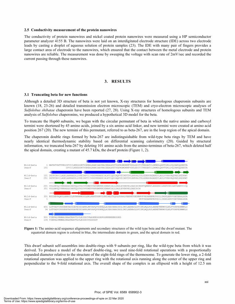
2.5 Conductivity measurement of the protein nanowires
The conductivity of protein nanowires and nickel coated protein nanowires were measured using a HP semiconductor parameter analyzer 4155 B. The nanowires were laid on an interdigitated electrode structure (IDE) across two electrode leads by casting a droplet of aqueous solution of protein samples (23). The IDE with many pair of fingers provides a large contact area of electrode to the nanowires, which ensured that the contact between the metal electrode and protein nanowires are reliable. The measurement was done by sweeping the voltage with scan rate of 2mV/sec and recorded the current passing through these nanowires.
3. RESULTS
3.1 Truncating beta for new functions
Although a detailed 3D structure of beta is not yet known, X-ray structures for homologous chaperonin subunits are known (18, 23-26) and detailed transmission electron microscopic (TEM) and cryo-electron microscopic analyses of Sulfolobus shibatae chaperonin have been reported (27, 28). Using X-ray structures of homologous subunits and TEM analysis of Sulfolobus chaperonins, we produced a hypothetical 3D model for the beta.
To truncate the Hsp60 subunits, we began with the circular permutant of beta in which the native amino and carboxyl termini were shortened by 45 amino acids, joined by a six amino acid linker, and new termini were created at amino acid position 267 (20). The new termini of this permutant, referred to as beta-267, are in the loop region of the apical domain.
The chaperonin double rings formed by beta-267 are indistinguishable from wild-type beta rings by TEM and have nearly identical thermodynamic stability based on differential scanning calorimetry (20). Guided by structural information, we truncated beta-267 by deleting 101 amino acids from the amino-terminus of beta-267, which deleted half the apical domain, creating a mutant of 45.7 kDa, the dwarf protein (Figure 1, 2).
Wild-beta 1 MATATVATTPEGIPVIILKEGSSRTYGKEALRANIAAVKAIEEALKSTYGPRGMDKMFVDSLGDITITNDGATILDKMDLQHPTGKLLVQIAKGQDEETA Dwarf 151 IPVIILKEGSSRTYGKEALRANIAAVKAIEEALKSTYGPRGMDKMFVDSLGDITITNDGATILDKMDLQHPTGKLLVQIAKGQDEETA Wild-beta 101 DGTKTAVILAGELAKKAEDLLYKEIHPTIIVSGYKKAEEIALKTIQDIAQPVSINDTDVLRKVALTSLGSKAVAGAREYLADLVVKAVAQVAELRGDKWY Dwarf 251 DGTKTAVILAGELAKKAEDLLYKEIHPTIIVSGYKKAEEIALKTIQDIAQPVSINDTDVLRKVALTSLGSKAVAGAREYLADLVVKAVAQVAELRGDKWY Wild-beta 201 VDLDNVQIVKKHGGSINDTQLVYGIVVDKEVVHPGMPKRIENAKIALLDASLEVEKPELDAEIRINDPTQMHKFLEEEENILKEKVDKIAATGANVVICQ Dwarf 351 VDLDNVQIVKKHGGSINDTQLVYGIVVDKEVVHPGMPKRIENAKIALLDASLEVEKPELDAEIRIN Wild-beta 301 KGIDEVAQHYLAKKGILAVRRAKKSDLEKLARATGGRVISNIDELTSQDLGYAALVEERKVGEDKMVFVEGAKNPKSVSILIRGGLERVVDETERALRDA Dwarf 1 MVFVEGAKNPKSVSILIRGGLERVVDETERALRDA Wild-beta 401 LGTVADVIRDGRAVAGGGAVEIEIAKRLRKYAPQVGGKEQLAIEAYANAIEGLIMILAENAGLDPIDKLMQLRSLHENETNKWYGLNLFTGNPEDMWKLG Dwarf 36 LGTVADVIRDGRAVAGGGAVEIEIAKRLRKYAPQVGGKEQLAIEAYANAIEGLIMILAENAGLDPIDKLMQLRSLHENETNKWYGLNLFTGNPEDMWKLG Wild-beta 501 VIEPALVKMNAIKAATEAVTLVLRIDDIVAAGKKGGSEPGGKKEKEEKSSED Dwarf 136 VIEPALVKMNAIKAATEAVTLVLRIDDIVGGSGGT
Figure 1: The amino-acid sequence alignments and secondary structures of the wild type beta and the dwarf mutant. The equatorial domain region is colored in blue, the intermediate domain in green, and the apical domain in red.
This dwarf subunit self-assembles into double-rings with 9 subunits per ring, like the wild-type beta from which it was derived. To produce a model of the dwarf double-ring, we used nine-fold rotational operations with a proportionally expanded diameter relative to the structure of the eight-fold rings of the thermosome. To generate the lower ring, a 2-fold rotational operation was applied to the upper ring with the rotational axis running along the center of the upper ring and perpendicular to the 9-fold rotational axis. The overall shape of the complex is an ellipsoid with a height of 12.5 nm
Proc. of SPIE Vol. 6589 658902-3
xxi
Downloaded From: https://www.spiedigitallibrary.org/conference-proceedings-of-spie on 22 Mar 2020Terms of Use: https://www.spiedigitallibrary.org/terms-of-use
Top view Sdp view
1125
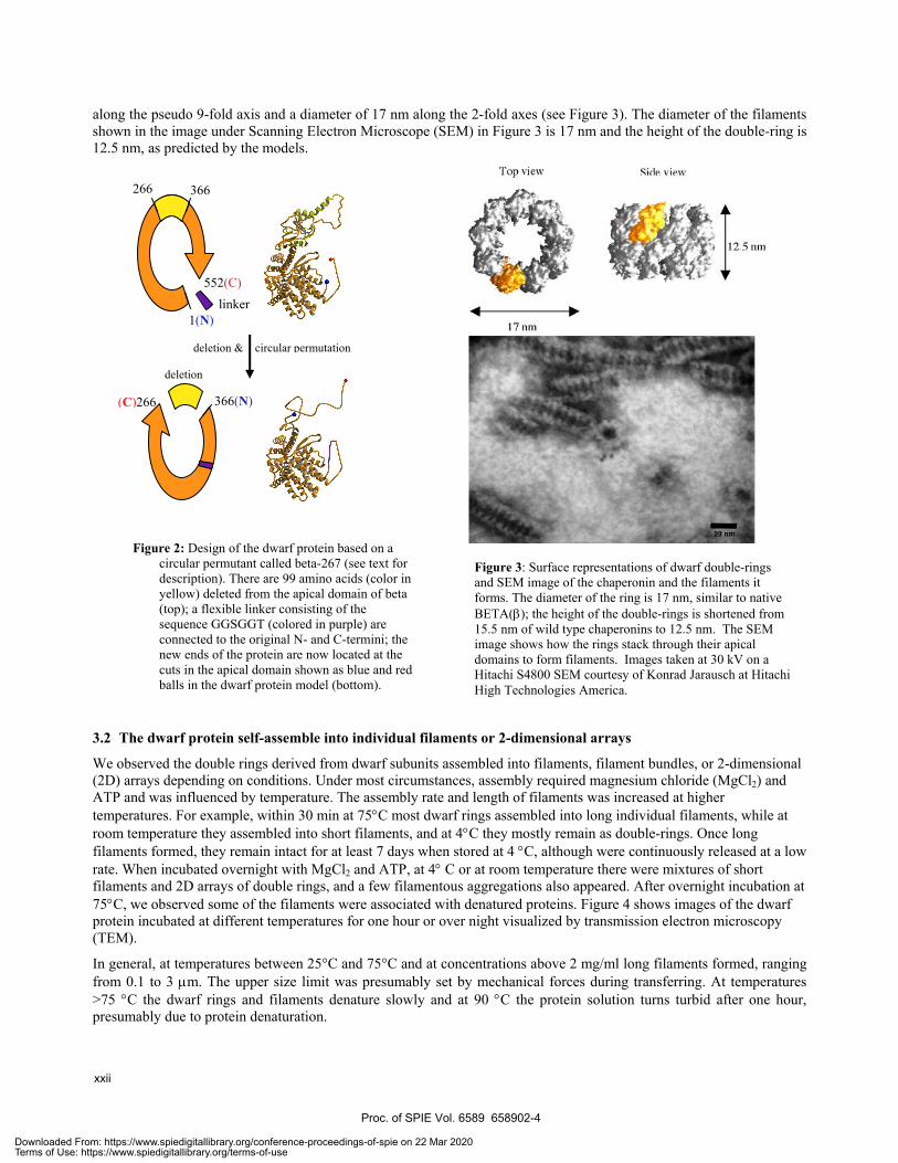
along the pseudo 9-fold axis and a diameter of 17 nm along the 2-fold axes (see Figure 3). The diameter of the filaments shown in the image under Scanning Electron Microscope (SEM) in Figure 3 is 17 nm and the height of the double-ring is 12.5 nm, as predicted by the models.
3.2 The dwarf protein self-assemble into individual filaments or 2-dimensional arrays
We observed the double rings derived from dwarf subunits assembled into filaments, filament bundles, or 2-dimensional (2D) arrays depending on conditions. Under most circumstances, assembly required magnesium chloride (MgCl2) and ATP and was influenced by temperature. The assembly rate and length of filaments was increased at higher temperatures. For example, within 30 min at 75°C most dwarf rings assembled into long individual filaments, while at room temperature they assembled into short filaments, and at 4°C they mostly remain as double-rings. Once long filaments formed, they remain intact for at least 7 days when stored at 4 °C, although were continuously released at a low rate. When incubated overnight with MgCl2 and ATP, at 4° C or at room temperature there were mixtures of short filaments and 2D arrays of double rings, and a few filamentous aggregations also appeared. After overnight incubation at 75°C, we observed some of the filaments were associated with denatured proteins. Figure 4 shows images of the dwarf protein incubated at different temperatures for one hour or over night visualized by transmission electron microscopy (TEM).
In general, at temperatures between 25°C and 75°C and at concentrations above 2 mg/ml long filaments formed, ranging from 0.1 to 3 µm. The upper size limit was presumably set by mechanical forces during transferring. At temperatures >75 °C the dwarf rings and filaments denature slowly and at 90 °C the protein solution turns turbid after one hour, presumably due to protein denaturation.
linker 1(N)
552(C)
266 366
366(N) (C)266
deletion
deletion & circular permutation
Figure 3: Surface representations of dwarf double-rings and SEM image of the chaperonin and the filaments it forms. The diameter of the ring is 17 nm, similar to native BETA(β); the height of the double-rings is shortened from 15.5 nm of wild type chaperonins to 12.5 nm. The SEM image shows how the rings stack through their apical domains to form filaments. Images taken at 30 kV on a Hitachi S4800 SEM courtesy of Konrad Jarausch at Hitachi High Technologies America.
Figure 2: Design of the dwarf protein based on a circular permutant called beta-267 (see text for description). There are 99 amino acids (color in yellow) deleted from the apical domain of beta (top); a flexible linker consisting of the sequence GGSGGT (colored in purple) are connected to the original N- and C-termini; the new ends of the protein are now located at the cuts in the apical domain shown as blue and red balls in the dwarf protein model (bottom).
Proc. of SPIE Vol. 6589 658902-4
xxii
Downloaded From: https://www.spiedigitallibrary.org/conference-proceedings-of-spie on 22 Mar 2020Terms of Use: https://www.spiedigitallibrary.org/terms-of-use

(e)
55*
1
I_(f)
• S.
- •
•
4* I•S
Figure 4: TEM images of the dwarf protein incubated with NaCl, MgCl2, and ATP at different temperatures for one hour or over
night. After one-hour incubation (a) at 75 °C most of the rings are incorporated into long single filaments; (b) at room temperature short filaments are assembled; (c) at 4 °C most of the proteins remain as double-rings. When incubated over night (d) at 75 °C some denatured proteins precipitate on filaments; (e) at room temperature 2D arrays are formed; (f) at 4 °C dwarf protein filamentous aggregations appear.
3.3 Other factors affecting filament formation
The dwarf subunit concentrations and ATP/Mg were important for both the assembly of rings and ring association into filaments. Without ATP/Mg at 4 °C or room temperature, we observed few filaments and bundles by TEM. At 75 °C after one hour, we observed mostly aggregates. At higher concentrations of dwarf subunits (> 6 mg/m), a few filaments assembled without ATP/Mg.
Proc. of SPIE Vol. 6589 658902-5
xxiii
Downloaded From: https://www.spiedigitallibrary.org/conference-proceedings-of-spie on 22 Mar 2020Terms of Use: https://www.spiedigitallibrary.org/terms-of-use
lip
I!
We also observed that dwarf subunit assembly depended on the order of addition of reagents. That is, assembly into individual filaments required that ATP/Mg was added to a mixture of protein in buffer. If the protein was added to a solution of ATP/Mg and buffer, bundles formed rather than individual filament.
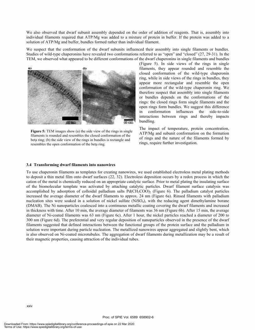
We suspect that the conformation of the dwarf subunits influenced their assembly into single filaments or bundles. Studies of wild-type chaperonins have revealed two conformations referred to as “open” and “closed” (27, 29-31). In the TEM, we observed what appeared to be different conformations of the dwarf chaperonins in single filaments and bundles
(Figure 5). In side views of the rings in single filaments, they appear rounded and resemble the closed conformation of the wild-type chaperonin ring, while in side views of the rings in bundles, they appear more rectangular and resemble the open conformation of the wild-type chaperonin ring. We therefore suspect that assembly into single filaments or bundles depends on the conformations of the rings: the closed rings form single filaments and the open rings form bundles. We suggest this difference in conformation influences the side-to-side interactions between rings and thereby impacts bundling.
The impact of temperature, protein concentration, ATP/Mg and subunit conformation on the formation of rings and the nature of the filaments formed by rings, require further investigation.
3.4 Transforming dwarf filaments into nanowires
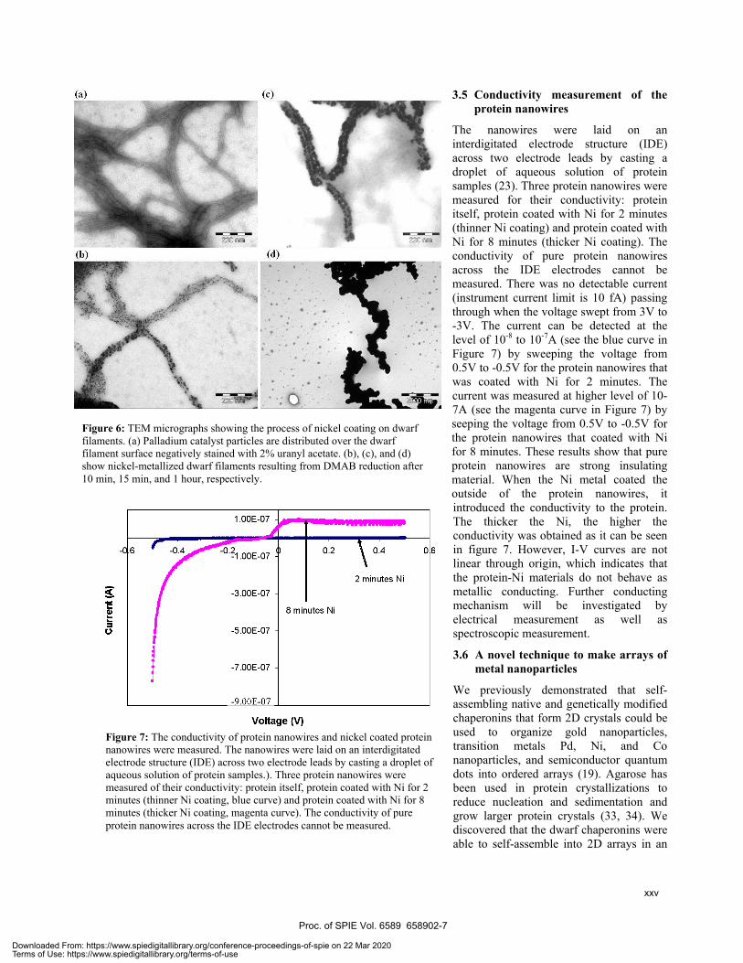
To use chaperonin filaments as templates for creating nanowires, we used established electroless metal plating methods to deposit a thin metal film onto dwarf surfaces (22, 32). Electroless deposition occurs by a redox process in which the cation of the metal is chemically reduced on an appropriate catalytic surface. Prior to metal plating the insulating surface of the biomolecular template was activated by attaching catalytic particles. Dwarf filament surface catalysis was accomplished by adsorption of colloidal palladium salts Pd(CH3COO)2 (Figure 6). The palladium catalyst particles increased the average diameter of the dwarf filaments to approx. 24 nm (Figure 6a). Rinsed filaments with palladium nucleation sites were soaked in a solution of nickel sulfate (NiSO4), with the reducing agent dimethylamine borane (DMAB). The Ni nanoparticles coalesced into a continuous metallic coating covering the dwarf filaments and increased in thickness with time. After 10 min, the average diameter of filaments was 36 nm (Figure 6b). After 15 min, the average diameter of Ni-coated filaments was 63 nm (Figure 6c). After 1 hour, the nickel particles reached a diameter of 200 to 300 nm (Figure 6d). The preferential and very regular deposition of nanoparticles observed in the presence of the dwarf filaments suggested that defined interactions between the functional groups of the protein surface and the palladium in solution were important during particle nucleation. The metallized nanowires appear aggregated and slightly bent, which is also observed on Ni-coated microtubules. The aggregation of dwarf filaments during metallization may be a result of their magnetic properties, causing attraction of the individual tubes.
Figure 5: TEM images show (a) the side view of the rings in single filaments is rounded and resembles the closed conformation of the beta ring; (b) the side view of the rings in bundles is rectangle and resembles the open conformation of the beta ring.
Proc. of SPIE Vol. 6589 658902-6
xxiv
Downloaded From: https://www.spiedigitallibrary.org/conference-proceedings-of-spie on 22 Mar 2020Terms of Use: https://www.spiedigitallibrary.org/terms-of-use
(c)
(d)
*
* t.
-3.OOE-07
-5.OOE-07
-7.OOE-07
8 minutes Ni
Voltage (V)
3.5 Conductivity measurement of the protein nanowires
The nanowires were laid on an interdigitated electrode structure (IDE) across two electrode leads by casting a droplet of aqueous solution of protein samples (23). Three protein nanowires were measured for their conductivity: protein itself, protein coated with Ni for 2 minutes (thinner Ni coating) and protein coated with Ni for 8 minutes (thicker Ni coating). The conductivity of pure protein nanowires across the IDE electrodes cannot be measured. There was no detectable current (instrument current limit is 10 fA) passing through when the voltage swept from 3V to -3V. The current can be detected at the level of 10-8 to 10-7A (see the blue curve in Figure 7) by sweeping the voltage from 0.5V to -0.5V for the protein nanowires that was coated with Ni for 2 minutes. The current was measured at higher level of 10-7A (see the magenta curve in Figure 7) by seeping the voltage from 0.5V to -0.5V for the protein nanowires that coated with Ni for 8 minutes. These results show that pure protein nanowires are strong insulating material. When the Ni metal coated the outside of the protein nanowires, it introduced the conductivity to the protein. The thicker the Ni, the higher the conductivity was obtained as it can be seen in figure 7. However, I-V curves are not linear through origin, which indicates that the protein-Ni materials do not behave as metallic conducting. Further conducting mechanism will be investigated by electrical measurement as well as spectroscopic measurement.
3.6 A novel technique to make arrays of metal nanoparticles
We previously demonstrated that self-assembling native and genetically modified chaperonins that form 2D crystals could be used to organize gold nanoparticles, transition metals Pd, Ni, and Co nanoparticles, and semiconductor quantum dots into ordered arrays (19). Agarose has been used in protein crystallizations to reduce nucleation and sedimentation and grow larger protein crystals (33, 34). We discovered that the dwarf chaperonins were able to self-assemble into 2D arrays in an
Figure 6: TEM micrographs showing the process of nickel coating on dwarf filaments. (a) Palladium catalyst particles are distributed over the dwarf filament surface negatively stained with 2% uranyl acetate. (b), (c), and (d) show nickel-metallized dwarf filaments resulting from DMAB reduction after 10 min, 15 min, and 1 hour, respectively.
Figure 7: The conductivity of protein nanowires and nickel coated protein nanowires were measured. The nanowires were laid on an interdigitated electrode structure (IDE) across two electrode leads by casting a droplet of aqueous solution of protein samples.). Three protein nanowires were measured of their conductivity: protein itself, protein coated with Ni for 2 minutes (thinner Ni coating, blue curve) and protein coated with Ni for 8 minutes (thicker Ni coating, magenta curve). The conductivity of pure protein nanowires across the IDE electrodes cannot be measured.
Proc. of SPIE Vol. 6589 658902-7
xxv
Downloaded From: https://www.spiedigitallibrary.org/conference-proceedings-of-spie on 22 Mar 2020Terms of Use: https://www.spiedigitallibrary.org/terms-of-use
I
—
agarose matix. We optimized the concentration of agarose so that its melting temperature was below 75°C, which allowed us to take advantage of the thermal stability of the chaperonins. We discovered that uranyl acetate (UA) does not stain agarose and we used UA to visualize dwarf rings, filaments, and 2D arrays by TEM in agarose gel slices.
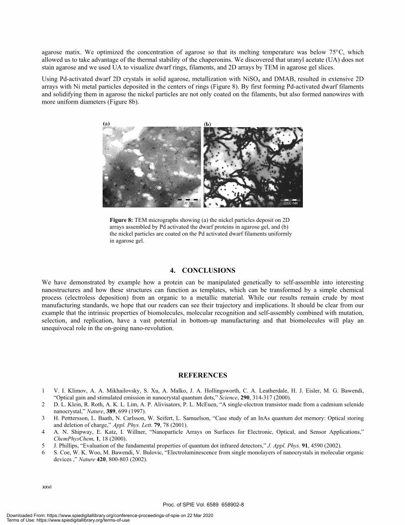
Using Pd-activated dwarf 2D crystals in solid agarose, metallization with NiSO4 and DMAB, resulted in extensive 2D arrays with Ni metal particles deposited in the centers of rings (Figure 8). By first forming Pd-activated dwarf filaments and solidifying them in agarose the nickel particles are not only coated on the filaments, but also formed nanowires with more uniform diameters (Figure 8b).
4. CONCLUSIONS We have demonstrated by example how a protein can be manipulated genetically to self-assemble into interesting nanostructures and how these structures can function as templates, which can be transformed by a simple chemical process (electroless deposition) from an organic to a metallic material. While our results remain crude by most manufacturing standards, we hope that our readers can see their trajectory and implications. It should be clear from our example that the intrinsic properties of biomolecules, molecular recognition and self-assembly combined with mutation, selection, and replication, have a vast potential in bottom-up manufacturing and that biomolecules will play an unequivocal role in the on-going nano-revolution.
REFERENCES
1 V. I. Klimov, A. A. Mikhailovsky, S. Xu, A. Malko, J. A. Hollingsworth, C. A. Leatherdale, H. J. Eisler, M. G. Bawendi, “Optical gain and stimulated emission in nanocrystal quantum dots,” Science, 290, 314-317 (2000).
2 D. L. Klein, R. Roth, A. K. L. Lim, A. P. Alivisators, P. L. McEuen, “A single-electron transistor made from a cadmium selenide nanocrystal,” Nature, 389, 699 (1997).
3 H. Petttersson, L. Baath, N. Carlsson, W. Seifert, L. Samuelson, “Case study of an InAs quantum dot memory: Optical storing and deletion of charge,” Appl. Phys. Lett. 79, 78 (2001).
4 A. N. Shipway, E. Katz, I. Willner, “Nanoparticle Arrays on Surfaces for Electronic, Optical, and Sensor Applications,” ChemPhysChem, 1, 18 (2000).
5 J. Phillips, “Evaluation of the fundamental properties of quantum dot infrared detectors,” J. Appl. Phys. 91, 4590 (2002). 6 S. Coe, W. K. Woo, M. Bawendi, V. Bulovic, “Electroluminescence from single monolayers of nanocrystals in molecular organic
devices ,” Nature 420, 800-803 (2002).
Figure 8: TEM micrographs showing (a) the nickel particles deposit on 2D arrays assembled by Pd activated the dwarf proteins in agarose gel, and (b) the nickel particles are coated on the Pd activated dwarf filaments uniformly in agarose gel.
Proc. of SPIE Vol. 6589 658902-8
xxvi
Downloaded From: https://www.spiedigitallibrary.org/conference-proceedings-of-spie on 22 Mar 2020Terms of Use: https://www.spiedigitallibrary.org/terms-of-use
7 Y. Xia, P. Yang, Y. Sun, Y. Wu, B. Mayers, B. Gates, Y. Yin, F. Kim, H. Yan, “One-dimensional nanostructures: synthesis, characterization, and applications,” Adv. Mater. 15, 353-389 (2003).
8 S. Behrens, J. Wu, W. Habicht, E. Unger “Silver nanoparticles and nanowire formation by microtubule templates,” Chem. Mater. 16, 3085-3090 (2004).
9 T. Scheibel, R. Parthasarathy, G. Sawicki, X. M. Lin, H. Jaeger, S. Lindquist, “Conducting nanowires built by controlled self-assembly of amyloid fibers and selective metal deposition,” Proc. Natl Acad. Sci. USA 100, 4527-4532 (2003).
10 S. W. Lee, C. Mao, C. E. Flynn, A. M. Blecher, “Ordering of quantum dots using genetically engineered viruses,” Science 296, 892-895 (2000).
11 S. R. Whaley, D. S. English, E. L. Hu, P. F. Barbara, A. M. Belcher, “Selection of peptides with semiconductor binding specificity for directed nanocrystal assembly,” Nature 405, 665-668 (2000).
12 C. M. Niemeyer, “Self-assembled nanostructures based on DNA: towards the development of nanobiotechnology,” Curr. Opin. Chem. Biol. 4, 609-618 (2000).
13 W. Fritzsche, K. Bohm, E. Unger, J. K. Kohler, “Metallic nanowires created by biopolymer masking, ” Appl. Phys. Lett. 75, 2854-2856 (1999).
14 E. Braun, Y. Eichen, U. Sivan, G. Ben-Yoseph, “DNA-templated assembly and electrode attachment of a conducting silver wire,” Nature 391, 775-778 (1998).
15 H. K. Kagawa, T. Yaoi, L. Brocchieri, R. A. McMillan, T. Alton, J. D. Trent, “The composition, structure and stability of a group II chaperonin are temperature regulated in a hyperthermophilic archaeon,” Mol. Microbiol. 48, 143-156 (2003).
16 J. D. Trent, H. K. Kagawa, T. Yaoi, E. Olle, N. J. Zaluzec, “Chaperonin filaments: the archaeal cytoskeleton?” Proc. Natl Acad. Sci. USA 94, 5383-5388 (1997).
17 H. K. Kagawa, J. Osipiuk, N. Maltsev, R. Overbeek, E. Quaite-Randall, A. Joachimiak, J. D. Trent, “The 60 kDa heat shock proteins in the hyperthermophilic archaeon Sulfolobus shibatae,” J. Mol. Biol. 253, 712-725 (1995).
18 L. Ditzel, J. Lowe, D. Stock, K. O. Stetter, H. Huber, R. Huber, S. Steinbacher, “Crystal structure of the thermosome, the archaeal chaperonin and homolog of CCT,” Cell, 93, 125-138 (1998).
19 R. A. McMillan, J. Howard, N. Z. Zaluzec, H. K. Kagawa, R. Mogul, Y. Li, C. D. Paavola and J. D. Trent, “A self-assembliing protein template for constrained synthesis patterning of nanoparticle arrays,” J. Am. Chem. Soc. 127, 2800-2801 (2005).
20 C. D. Paavola, S. L. Chan, Y. Li, R. A. McMillan, J. D. Trent, “A versatile platform for nanotechnology based on circular permutation of a chaperonin protein,” Nanotechnology 17, 1171-1176 (2006).
21 F. M. Ausubel, R. Brent, R. E. Kingston., D. D. Moore, J. G. Seidman, K. Struhl, eds Current Protocols in Molecular Biology, Wiley, New York (1998).
22 R. Kirsch, M. Mertig, W. Pompe, G. Sadowski, K. J. Bohm, E. Unger, “Three-dimensional metallization of microtubules,” Thin Solid Films 305, 248-253 (1997).
23 P. Young, Y. Lu, R. Terrill and J. Li, “High-sensitivity NO2 detection with carbon nanotube-gold nanoparticle composite films,” J. Nanosci. Nanotechnol. 5, 1509-1513 (2005).
24 G. Pappenberger, J. A. Wilsher, S. M. Roe, D. J. Counsell, K. R. Willison, L. H. Pearl, “Crystal structure of the CCTg apical domain: implications for substrate binding to the eukaryotic cytosolic chaperonin,” J. Mol. Biol. 318, 1367-1379 (2002).
25 K. Braig., M. Simon, F. Furuya, J. F. Hainfeld, A. L. Horwich, “The crystal structure of bacterial chaperonin GroEL at 2.8 Å,” Nature, 13, 578-586 (1994).
26 Z. Xu, A. L. Horwich, P. B. Sugker, “The crystal structure of the asymmetric GroEL-GroES-(ADP)7 chaperonin complex,” Nature 388, 741-750 (1997).
27 G. Schoehn, E. Quaite-Randall, J. L. Jimenez, A. Joachimiak, H. R. Saibil, “Three conformations of an archaeal chaperonin, TF55 from Sulfolobus shibatae,” J. Mol. Biol. 296, 813-819 (2000).
28 P. J. Koeck., H. K. Kagawa, M. J. Ellis, H. Hebert, J. D. Trent, “Two-dimensional crystals reconstituted beta-subunits of the chaperonin TF55 from Sulfolobus shibatae,” Biochim Biophys Acta, 1429, 40-44 (1998).
29 E. Quaite-Ramdall, J. D. Trent, R. Josephs, A. Joachimiak, “Conformational cycle of the archaeosome, a TCP1-like chaperonin from Sulfolobus shibatae,” Biol. Chem. 270, 28818-28823 (1995).
30 I. Gustche, O. Mihalache, W. Baumeister, “ATPase cycle of an archaeal chaperonin,” J. Mol. Biol. 300, 187-196 (2000). 31 I. Gustche, J. Holzinger, N. Rauh, W. Baumeister, R. P. May, “ATP-induced structural change of the thermosome is temperature-
dependent,” J. Stru. Biol. 135, 139-146 (2001). 32 M. Mertig, R. Kirsch, W. Pompe, “Biomolecular approach to nanotube fabrication,” Appl. Phys. A 66, S723-S727 (1998). 33 M. C. Robert, F. Lefaucheux, “Crystal growth in gels: principle and application,” J. Cryst. Growth. 90, 358-367 (1988). 34 J. M. Garcia-Ruiz, A. Hernandez-Hernndez, J. Lopez-Jaramillo, B. Thomas, “Crystallization screening directly in electrophoresis
gels,” J. Crystl. Growth. 232, 596-602 (2001).
Proc. of SPIE Vol. 6589 658902-9
xxvii
Downloaded From: https://www.spiedigitallibrary.org/conference-proceedings-of-spie on 22 Mar 2020Terms of Use: https://www.spiedigitallibrary.org/terms-of-use

Downloaded From: https://www.spiedigitallibrary.org/conference-proceedings-of-spie on 22 Mar 2020Terms of Use: https://www.spiedigitallibrary.org/terms-of-use

Research in Micro- Nano- technology and systems: a European perspective. Opportunities in Framework Programme 7: 2007-2013
I. Vergara, G. Van Caenegem and F. Ibáñez 1
European Commission. DG Information Society and Media. Microsystems. Belgium
ABSTRACT
The Research European Programmes have paid attention to the area of microsystems since the early 90's when the Research was focused on Micro-Electro-Mechanical Systems. Since then the interest has grown into an area of Microsystems and Micro Nano Technology for a wide set of applications in which the multidiscipline and the convergence of technologies play an important role. Systems combining sensing, processing and actuating are increasingly complex involving different disciplines and integrating different technologies, and making the field of Microsystems technology expands to the field of 'Smart Integrated Systems'. Today the attention is focused in the increasing complexity and miniaturization of the systems, networking capabilities and autonomy. The recently launched 7th Framework Programme and the coordination of national or regional research initiatives will help to realise the research agenda for this strategic field for Europe. This paper will give some results of ongoing initiatives, some visions and an outlook for the future with focus in micro and nanosytems. Keywords: Microsystems, Smart Systems, European Framework Programme
1. INTRODUCTION The European Union (EU) has recognized the importance of the Research and Technological Development (RTD) for a country's economic growth since the earliest European Treaties in the 50's. Indeed, the competitiveness of companies and the employment they can provide depend, to a great extent, on RTD activities, especially those combining research resources in certain key areas and priority technologies. An important part of the research investments in Europe goes to the Information and Communication Technologies (ICT) area which accounts for about 40% of Europe's productivity1 growth. In June 2005, the EC adopted the i2010 initiative2 in which one of the policy priorities is an 80% increase in EU-wide investment in research on Information and Communication Technologies by 2010. This is necessary because Europe’s investment in ICT is still behind that of Japan and the US. Europe invests only 80€ per head compared to 350€ in the US and 400€ in Japan3. The situation for Europe could become even worse if the R&D growth rates of India and China or the rest of South East Asia countries are maintained, reflecting the importance these countries attach to ICT technologies. There is a need to focus the research efforts on areas where Europe has recognized strengths and on new areas with high potential which must be identified with the active involvement of industry. Smart Systems Integration is one of the most important drivers of ICT, and it is also one of those promising areas where European countries have today a good competitive position, as European industry is a world leader in microsystems and related advanced technologies. The main Research instrument in the EU is the Research and Technological Development Framework Programme (FP), where, since 1984, EU-level research and demonstration activities are funded. It was during the 4th Framework Programme (FP4) (1994-1998) when the European Commission started to pay attention to the area of MST with focus on Micro-Electro-Mechanical Systems (MEMS). The research interest started to move from MEMS towards Micro and Nanosystems (MNS) and Micro and Nanotechnologies (MNT) with the 5th Framework Programme (FP5) (1998-2002) in which the Information Society Technologies (IST) Programme emphasized the industrial applications of MEMS and MOEMS (Micro-Opto-Electro-Mechanical Systems). During the recently concluded 6th Framework Programme (FP6) (2002-2006), the attention has kept in the industrial applications of the systems covering all steps needed to form systems out of components, systems that are able to take information from the environment through sensors, to process it
1 The views developed in this article are that of the authors and do not reflect necessarily the position of the European Commission.
Plenary Paper
Nanotechnology III, edited by Fernando Briones,Proc. of SPIE Vol. 6591, 659102, (2007)
0277-786X/07/$18 · doi: 10.1117/12.740799
Proc. of SPIE Vol. 6591 659102-1
xxix
Downloaded From: https://www.spiedigitallibrary.org/conference-proceedings-of-spie on 22 Mar 2020Terms of Use: https://www.spiedigitallibrary.org/terms-of-use
electronically, to communicate it and to ‘close the loop’ by taking the appropriate action. Systems combining sensing, processing and actuating are increasingly complex involving different disciplines and integrating different technologies, and making the field of Microsystems technology expands to the field of 'Smart Integrated Systems'. Other important European initiatives emerging during the last years of FP6 are the European Technology Platforms (ETPs). ETPs provide a framework for stakeholders, including key industrial players, SMEs, public authorities, and the research community, in order to define research and development priorities, timeframes and action plans on a number of strategically important issues with industry taking the lead role. In this way, the ETPs are focused on future markets for key technologies and help Europe to keep its leadership in relevant areas. So far, 31 ETPs have been launched covering a wide range of technological challenges.4 In the ICT area there are currently 9 related ETPs active in areas such as Satellite communications, Robotics, Photonics, or just to mention the three ETPs more related to MST, Nanoelectronics, Embedded Systems and Smart Systems Integration. In January 2007, the 7th Framework Programme (FP7) was launched for the duration of seven years, from 2007 to 2013. The European Commission (EC) budget for these seven years is €50.5 billion, which represents a 41% increase from FP6 at 2004 prices and 63% at current prices. Similarly to previous FPs, FP7 supports research in selected priority areas aiming at making or keeping the EU as a world leader in those sectors. ICT continues being one of these priority themes in which the efforts will concentrate in areas with strategic importance where we expect to get the most out of our investments. The MST or smart systems integration is one of those promising areas. After this short introduction, the article will first make a review of the activities funded under FP6 in the MST area. Then it will make a summary of the current European initiatives of the area. Finally, the main characteristics of FP7 will be presented giving some visions and an outlook for the future research on MST.
2. ACTIVITIES IN THE MICROSYSTEMS AREA UNDER FP6 The 6th Framework Programme has been active during the period from 2002 to 2006 supporting research in seven thematic priorities, being IST one of them. The total EC budget of FP6 was € 16.27 billion and the EC budget devoted to IST priority has been €3.625 billion for the four years of duration of the Programme. The research on microsystems was very relevant in the IST area whose actions addressed four technological priorities: A) Integrating research into technological areas of priority interest for citizens and businesses; B) Communication and computing infrastructure; C) Components and microsystems; and D) Information management and interfaces. A total of six calls for proposals have been open in the IST priority in FP6. The microsystems objective was present, in a minor or larger extent, in all of them. As a result, 79 projects are currently being or have been funded in the area of micro and nanosystems, representing a total budget of €507 million, of which the EC contributes €301 million. All these projects have brought together researchers and industries from both end users and suppliers from about 500 different organizations coming from all member states, associated countries and other countries outside the EU. The group of projects have successfully covered a complementary set of activities, ranging from technologies and systems development (e.g. MEMS, RF microsystems, plastic and organic micro-nanosystems), to product innovation and new manufacturing processes. The use of microsystems to support applications, such as health and biomedicine, food chain management, displays and robotics have also been largely covered by the portfolio of projects. Taking into account the activities of the project, we have classified the projects in six different groups:
1. Micro nano bio convergence systems 2. Sensor based systems and storage 3. Organic and large area electronics and display systems 4. Micro and nanosystems for Ambient Intelligence (AmI) 5. Manufacturing and process integration 6. Smart fabrics and interactive textiles 7. Support and coordination actions
Proc. of SPIE Vol. 6591 659102-2
xxx
Downloaded From: https://www.spiedigitallibrary.org/conference-proceedings-of-spie on 22 Mar 2020Terms of Use: https://www.spiedigitallibrary.org/terms-of-use

MSI&MNTSOLUTIONS
-dAt malgQ..Iaycc©tP[dI
FdFd
R$
AGROFOOD )MARKET NEEDS
Distribution of FP6 "Microsystems" budget by thematic clusterTotal budget: 301 M€
35%
18%18%
11%
10%
6% 2% Nano Bio ICT (NBIC)
Sensor based Systems andStorageOrganic/Large area electronicsand DisplaysMicro/Nanosystems for AmI
Manufacturing/processesintegrationSmart fabrics/Interactive textiles
Support and CoordinationActions
Figure 1: Distribution of the FP6 budget of the Micro- and Nanosystems Unit by thematic cluster.
Figure 1 shows the distribution of the FP6 EC budget between the different groups of projects mentioned above. The first group is made with projects dealing with the convergence of micro/nano, bio and information technologies. This is an emerging interdisciplinary area studying the interactions between living and artificial systems in different scales for the design of artifacts that improve or expand human cognitive and communicative capabilities, health and social well-being5. A total of 24 projects have been funded in this area including six large Integrated Projects (IP), and covering applications which go from health care to food quality monitoring. This group of projects has taken more than one third of the total FP6 budget of the Microsystems Unit, showing the importance and the interest of this new field. As an example, figure 2 shows the main objectives and characteristics of two of the projects included in this group. The first project is GOODFOOD, an IP that aims at developing a new generation of analytical methods based on Micro and Nanotechnologies solutions for the safety and quality assurance along the food chain in the agrofood industry. The second project showed in figure 2 is MASCOT, a Specific Targeted Research Project (STRP) aiming at creating a low-cost minimally-invasive intelligent system for the magnetic isolation and analysis of single circulating tumor cells for oncology diagnosis and therapy follow-up.
MASCOT Integrated microsystem for the magnetic isolation and analysis of single circulating tumor cells for oncology diagnostics and therapy follow-upCoordinator: IMEC (B)N. Partners: 7 from 6 countriesTotal budget: 4.27 M€EC funding: 2.5 M€Duration: 3 years (2006-2008)
GOODFOOD Food safety and quality monitoring with microsystems
Coordinator: CSIC (E)N. Partners: 29 from 10 countriesTotal budget: 17.43 M€EC funding: 9 M€Duration: 3.5 years (2004-2007)
RNA extraction & amplification
DNA detection
cell isolation & detection
Biosensor arrays for DNA detection
microsystemfor RNA extraction &
amplification
novel mRNA markersfor CTC characterization
microsystemfor immuno-magnetic cell
isolation & detection
novel CTC surface markersfor immuno-separation
RNA extraction & amplification
DNA detection
cell isolation & detection
Biosensor arrays for DNA detection
microsystemfor RNA extraction &
amplification
novel mRNA markersfor CTC characterizationnovel mRNA markers
for CTC characterization
microsystemfor immuno-magnetic cell
isolation & detection
novel CTC surface markersfor immuno-separation
Figure 2: Schematic representation of two examples of projects of the Micro Nano Bio Systems group: Goodfood is an example of large IP and MASCOT is an example of a STRP.
Proc. of SPIE Vol. 6591 659102-3
xxxi
Downloaded From: https://www.spiedigitallibrary.org/conference-proceedings-of-spie on 22 Mar 2020Terms of Use: https://www.spiedigitallibrary.org/terms-of-use
The second biggest group in relation to budget distribution is the one dealing with sensor based systems and storage. This group includes a number of projects in which sensing is an important part of their activities, excluding biosensing. The main topics covered are MEMS based oscillators, MEMS for RF and millimeter wave communications, small 3D sensing cubes, position sensor based on magnetoresistive nano-contacts, olfaction sensors, sensors for automatic handling of nano-objects, fully autonomous helicopter, and vibration energy scavenging. Projects dealing with innovative mass storage systems are also included in this group. A total of 14 projects including 3 IPs and 2 Networks of Excellence (NoE) build up this group. The third group deals with electronic technologies based on R&D on organic materials which can be cost effective even for large areas, and with projects over Display systems which often make use of emerging technologies related to organic materials. As an example, the objectives of some of the projects included in this group are: the applications of polymer electronics and the development of underlying technologies; research on novel materials, devices, handling and production methods for flexible displays; roll-to-roll manufacturing technology for flexible OLED devices; contact printing of electronics and opto-electronics; and smart high-integration flex technologies. Projects in the displays subgroup focus on the industrialization of emerging displays technologies related to organic materials, lightweight microdisplays, large size displays and 3D displays. A total of 11 projects, including 4 IPs build up the group. All projects with a general view on the use of micro and nanosystems for ambient intelligence (AmI) applications have also been grouped. The emphasis is on user-friendliness, efficient and distributed services support, user empowerment, and support for human activities. Examples of topics covered by the 5 projects (including 3 IPs) which build up this group are microsystems platform for context-aware mobile services and applications; or networked multisensor system for elderly people covering health care, safety, and security in home environments. There is also an important number of projects that deals with microsystems manufacturing technologies, from design to packaging, testing and reliability. Examples of topics including in this group, made up of 10 projects (including 3 IPs and 1 NoE) are: packaging, lithography techniques, high density integration and batch integration. A number of "service actions" projects under the umbrella of EUROPRACTICE supporting academic research, feasibility research, prototyping, training and education in the manufacturing sector are also included in the group. The 4 projects (2 of them IPs) included in the group on smart fabrics and interactive textiles form, together with three other projects funded under another area, the cluster of EC co-financed projects SFIT6. Examples of topics covered are the integration of advanced fibers and materials at the fiber core, microelectronics components, user interfaces (e.g. sensors, displays, speakers), power sources and embedded software, with the objective to fulfill user needs and expectations in terms of user-friendliness/functionality, cost, fabric resistance, comfort, robustness and reliable and accurate performance. Finally, the EC funds also projects for Specific Support Actions (SSA) or Coordination Actions (CA) in the area of microsystems. Examples of topics are: the creation of a European network pursuing the integration of new Member States and Accession Countries in the European Research Area; or to build roadmaps in various areas such as displays, RF micro-nanosystems, or applications of micro-nano-biotechnologies. This has been a summary of the activities funded by the EC during FP6 in the microsystems area. It is important to remark that R&D on microsystems could also be present, in a minor or larger extent, in other EC funded areas such as embedded systems, nanoelectronics ("more than Moore") or e-Health, or even in another priority areas such as NMP (Nanotechnologies, Materials and Production Processes).
3. OTHER EUROPEAN INITIATIVES IN THE AREA Together with the European Framework Programmes there are a number of other initiatives active in R&D of microsystems area, such as the European Research Area, under which the European Commission, Member States and the European Parliament, the scientific community and industry are committed to work together towards the creation of a non-fragmented internal market of research; the recently created Competitiveness and Innovation Programme (CIP); or the European Technology Platforms (ETPs). Due to the strategic role that the ETPs are currently playing in different
Proc. of SPIE Vol. 6591 659102-4
xxxii
Downloaded From: https://www.spiedigitallibrary.org/conference-proceedings-of-spie on 22 Mar 2020Terms of Use: https://www.spiedigitallibrary.org/terms-of-use
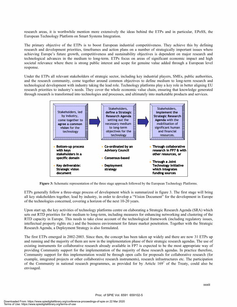
research areas, it is worthwhile mention more extensively the ideas behind the ETPs and in particular, EPoSS, the European Technology Platform on Smart Systems Integration. The primary objective of the ETPs is to boost European industrial competitiveness. They achieve this by defining research and development priorities, timeframes and action plans on a number of strategically important issues where achieving Europe’s future growth, competitiveness and sustainability objectives is dependent on major research and technological advances in the medium to long-term. ETPs focus on areas of significant economic impact and high societal relevance where there is strong public interest and scope for genuine value added through a European level response. Under the ETPs all relevant stakeholders of strategic sector, including key industrial players, SMEs, public authorities, and the research community, come together around common objectives to define medium to long-term research and technological development with industry taking the lead role. Technology platforms play a key role in better aligning EU research priorities to industry’s needs. They cover the whole economic value chain, ensuring that knowledge generated through research is transformed into technologies and processes, and ultimately into marketable products and services.
Stakeholders, led by industry,
come together toagree a common
vision for the technology
Stakeholders, define a StrategicResearch Agendasetting out the
necessary medium to long-term
objectives for thetechnology
Stakeholders, implement the
Strategic ResearchAgenda with the mobilisation of
significant humanand financialresources.
• Bottom-up process with keys stakeholders in a specific domain
• Key deliverable: Strategic vision document
• Co-ordinated by an Advisory Council
• Consensus-based
• Deployment strategy
• Through collaborative research in FP7 & with other resources, or
• Through a Joint Technology Initiative which integrates funding sources
Stakeholders, led by industry,
come together toagree a common
vision for the technology
Stakeholders, define a StrategicResearch Agendasetting out the
necessary medium to long-term
objectives for thetechnology
Stakeholders, implement the
Strategic ResearchAgenda with the mobilisation of
significant humanand financialresources.
• Bottom-up process with keys stakeholders in a specific domain
• Key deliverable: Strategic vision document
• Co-ordinated by an Advisory Council
• Consensus-based
• Deployment strategy
• Through collaborative research in FP7 & with other resources, or
• Through a Joint Technology Initiative which integrates funding sources
Figure 3: Schematic representation of the three stage approach followed by the European Technology Platforms. ETPs generally follow a three-stage process of development which is summarized in figure 3. The first stage will bring all key stakeholders together, lead by industry, in order to develop a “Vision Document” for the development in Europe of the technologies concerned, covering a horizon of the next 10-20 years. Upon start up, the key activities of technology platforms centre on elaborating a Strategic Research Agenda (SRA) which sets out RTD priorities for the medium to long-term, including measures for enhancing networking and clustering of the RTD capacity in Europe. This needs to take close account of the technological framework (including regulatory issues, intellectual property rights etc.) and the business environment for future market penetration. Together with the Strategic Research Agenda, a Deployment Strategy is also formulated. The first ETPs emerged in 2002-2003. Since then, the concept has been taken up widely and there are now 31 ETPs up and running and the majority of them are now in the implementation phase of their strategic research agendas. The use of existing instruments for collaborative research already available in FP7 is expected to be the most appropriate way of providing Community support for the implementation of the majority of these research agendas. In practice therefore, Community support for this implementation would be through open calls for proposals for collaborative research (for example, integrated projects or other collaborative research instruments), research infrastructures etc. The participation of the Community in national research programmes, as provided for by Article 1697 of the Treaty, could also be envisaged.
Proc. of SPIE Vol. 6591 659102-5
xxxiii
Downloaded From: https://www.spiedigitallibrary.org/conference-proceedings-of-spie on 22 Mar 2020Terms of Use: https://www.spiedigitallibrary.org/terms-of-use

EPCOS
M,k,i.Ueq,a1
Nevertheless, a limited number of research agendas can be expected to be of such an ambitious scale that they will require the mobilisation of very high public and private investments, as well as a large critical mass of researchers throughout Europe and even beyond. In view of establishing and co-ordinating the necessary public-private partnerships to implement such research agendas, a mechanism called Joint Technology Initiative (JTI) has been introduced. The JTIs are based on Treaty Article 1718, and are proposed as an effective means of meeting the needs of this small number of ETPs. Taking into account the stage of development of the Strategic Research Agendas of ETPs, six areas have been currently identified where a JTI could have particular relevance: hydrogen and fuel cells, aeronautics and air transport, innovative medicines, nano-electronics (ENIAC), embedded computing systems (ARTEMIS) and global monitoring for environment and security. In the area of Smart Systems Integration, the ETP EPoSS was launched in July 2006 by a group of industrial stakeholders (see figure 4) who are convinced that progress in research and development of smart systems and their integration techniques is crucial for European competitiveness.
Technology PlatformTechnology Platform
Figure 4: Main industrial stakeholders participating in the European Technology Platform on Smart Systems Integration, EPoSS.
Currently, European industry is the world leader in microsystems and related technologies; however there is a strong international competition which demands for a rapid product change, higher quality, lower cost and shorter time to markets. The future of microsystems will consist of integrated smart systems which are able to sense, and diagnose a situation and to decide the appropriate action. In order to keep the lead position of Europe in this area, there are a number of challenges to overcome and EPoSS will play a key role in ensuring an adequate focus of research funding in this industrially relevant area. The main objective of EPoSS is to provide a common European approach on innovative Smart Systems Integration from research to production. In order to do so, EPoSS has already formulated a common agreed roadmap and it is currently working in defining its implementation plan. The research priorities of EPoSS have been defined in its SRA and they represent the core fields of interest of the founding members of the ETP. In particular, these priorities are:
• Development of next-generation smart systems • Micro/nano/biotechnologies convergence • Integration and use of smart materials • Transfer from smart systems to viable products • Communication and data management for smart systems • Energy management for smart systems
Proc. of SPIE Vol. 6591 659102-6
xxxiv
Downloaded From: https://www.spiedigitallibrary.org/conference-proceedings-of-spie on 22 Mar 2020Terms of Use: https://www.spiedigitallibrary.org/terms-of-use
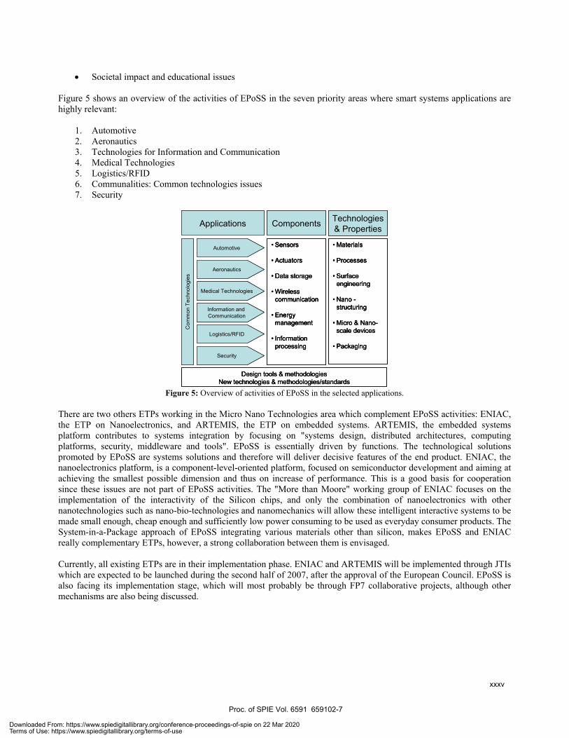
• Societal impact and educational issues Figure 5 shows an overview of the activities of EPoSS in the seven priority areas where smart systems applications are highly relevant:
1. Automotive 2. Aeronautics 3. Technologies for Information and Communication 4. Medical Technologies 5. Logistics/RFID 6. Communalities: Common technologies issues 7. Security
Automotive
Aeronautics
Medical Technologies
Information and Communication
Logistics/RFID
Security
Com
mon
Tec
hnol
ogie
s
Applications Components Technologies& Properties
• Sensors
• Actuators
• Data storage
• Wireless communication
• Energy management
• Information processing
• Materials
• Processes
• Surface engineering
• Nano -structuring
• Micro & Nano-scale devices
• Packaging
Design tools & methodologiesNew technologies & methodologies/standards
Automotive
Aeronautics
Medical Technologies
Information and Communication
Logistics/RFID
Security
Com
mon
Tec
hnol
ogie
s
Applications Components Technologies& Properties
• Sensors
• Actuators
• Data storage
• Wireless communication
• Energy management
• Information processing
• Sensors
• Actuators
• Data storage
• Wireless communication
• Energy management
• Information processing
• Materials
• Processes
• Surface engineering
• Nano -structuring
• Micro & Nano-scale devices
• Packaging
• Materials
• Processes
• Surface engineering
• Nano -structuring
• Micro & Nano-scale devices
• Packaging
Design tools & methodologiesNew technologies & methodologies/standards
Design tools & methodologiesNew technologies & methodologies/standards
Figure 5: Overview of activities of EPoSS in the selected applications. There are two others ETPs working in the Micro Nano Technologies area which complement EPoSS activities: ENIAC, the ETP on Nanoelectronics, and ARTEMIS, the ETP on embedded systems. ARTEMIS, the embedded systems platform contributes to systems integration by focusing on "systems design, distributed architectures, computing platforms, security, middleware and tools". EPoSS is essentially driven by functions. The technological solutions promoted by EPoSS are systems solutions and therefore will deliver decisive features of the end product. ENIAC, the nanoelectronics platform, is a component-level-oriented platform, focused on semiconductor development and aiming at achieving the smallest possible dimension and thus on increase of performance. This is a good basis for cooperation since these issues are not part of EPoSS activities. The "More than Moore" working group of ENIAC focuses on the implementation of the interactivity of the Silicon chips, and only the combination of nanoelectronics with other nanotechnologies such as nano-bio-technologies and nanomechanics will allow these intelligent interactive systems to be made small enough, cheap enough and sufficiently low power consuming to be used as everyday consumer products. The System-in-a-Package approach of EPoSS integrating various materials other than silicon, makes EPoSS and ENIAC really complementary ETPs, however, a strong collaboration between them is envisaged. Currently, all existing ETPs are in their implementation phase. ENIAC and ARTEMIS will be implemented through JTIs which are expected to be launched during the second half of 2007, after the approval of the European Council. EPoSS is also facing its implementation stage, which will most probably be through FP7 collaborative projects, although other mechanisms are also being discussed.
Proc. of SPIE Vol. 6591 659102-7
xxxv
Downloaded From: https://www.spiedigitallibrary.org/conference-proceedings-of-spie on 22 Mar 2020Terms of Use: https://www.spiedigitallibrary.org/terms-of-use
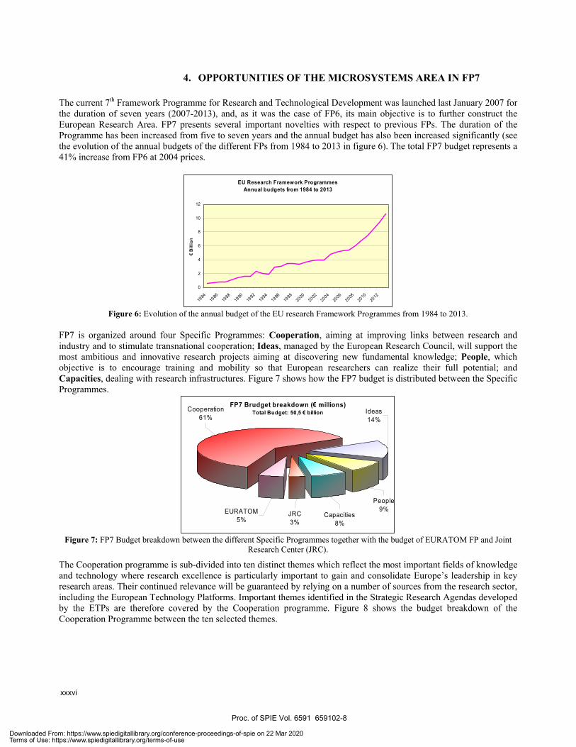
4. OPPORTUNITIES OF THE MICROSYSTEMS AREA IN FP7 The current 7th Framework Programme for Research and Technological Development was launched last January 2007 for the duration of seven years (2007-2013), and, as it was the case of FP6, its main objective is to further construct the European Research Area. FP7 presents several important novelties with respect to previous FPs. The duration of the Programme has been increased from five to seven years and the annual budget has also been increased significantly (see the evolution of the annual budgets of the different FPs from 1984 to 2013 in figure 6). The total FP7 budget represents a 41% increase from FP6 at 2004 prices.
EU Research Framework ProgrammesAnnual budgets from 1984 to 2013
0
2
4
6
8
10
12
1984
1986
1988
1990
1992
1994
1996
1998
2000
2002
2004
2006
2008
2010
2012
€ Bi
llion
Figure 6: Evolution of the annual budget of the EU research Framework Programmes from 1984 to 2013.
FP7 is organized around four Specific Programmes: Cooperation, aiming at improving links between research and industry and to stimulate transnational cooperation; Ideas, managed by the European Research Council, will support the most ambitious and innovative research projects aiming at discovering new fundamental knowledge; People, which objective is to encourage training and mobility so that European researchers can realize their full potential; and Capacities, dealing with research infrastructures. Figure 7 shows how the FP7 budget is distributed between the Specific Programmes.
FP7 Brudget breakdown (€ millions)Total Budget: 50,5 € billion
EURATOM5%
JRC 3%
Capacities8%
People 9%
Ideas14%
Cooperation61%
Figure 7: FP7 Budget breakdown between the different Specific Programmes together with the budget of EURATOM FP and Joint
Research Center (JRC).
The Cooperation programme is sub-divided into ten distinct themes which reflect the most important fields of knowledge and technology where research excellence is particularly important to gain and consolidate Europe’s leadership in key research areas. Their continued relevance will be guaranteed by relying on a number of sources from the research sector, including the European Technology Platforms. Important themes identified in the Strategic Research Agendas developed by the ETPs are therefore covered by the Cooperation programme. Figure 8 shows the budget breakdown of the Cooperation Programme between the ten selected themes.
Proc. of SPIE Vol. 6591 659102-8
xxxvi
Downloaded From: https://www.spiedigitallibrary.org/conference-proceedings-of-spie on 22 Mar 2020Terms of Use: https://www.spiedigitallibrary.org/terms-of-use

Cooperation Programme - thematic areas (€ million)
Transport€ 4160
Socio-econom ic sciences and hum anities
€ 623
Space€ 1430
Security€ 1400
Environm ent€ 1890 Energy
€ 2350
Nanosciences, Materials and new
Production Technologies
€ 3475
Inform ation and Com m unication
Technologies€ 9050
Food, agriclture , and biotechnology
€ 1935
Health€ 6100
Figure 8: Budget breakdown between the nice selected themes of the Cooperation Programme
4.1. Information and Communication Technologies theme. Challenge 3 "Components, Systems and Engineering" The work programme for the years 2007-2008 of the ICT theme of the FP7 Cooperation Programme was published in December 2006. This work programme defines the priorities for the three first calls for proposals of FP7, and it is structured around seven challenges that should be addressed if Europe is to be among the world leaders in next generation ICT and their applications. The challenges are driven either by industry and technology objectives or by socio-economic goals. Figure 9 shows a scheme of the seven ICT challenges.
Chal. 4
Digital Content &Knowledge
Chal. 5
ICT forHealth
Chal. 6
IntelligentCar &
SustainableGrowth
Chal. 7
ICT forIndepen-
dent Living& Inclusion
Chal. 1Network & ServiceInfrastructureChal. 2Cognitive Systems,Interaction, RoboticsChal. 3Components, Systemsand Engineering
End-to-end Systems, Socio-economic Goals
Tech
nolo
gy R
oadb
lock
s
Futu
re a
nd E
mer
ging
Te
chno
logi
es
TechnologyPlatforms
i2010 FlagshipInitiatives Chal. 4
Digital Content &Knowledge
Chal. 5
ICT forHealth
Chal. 6
IntelligentCar &
SustainableGrowth
Chal. 7
ICT forIndepen-
dent Living& Inclusion
Chal. 1Network & ServiceInfrastructureChal. 2Cognitive Systems,Interaction, RoboticsChal. 3Components, Systemsand Engineering
End-to-end Systems, Socio-economic Goals
Tech
nolo
gy R
oadb
lock
s
Chal. 4
Digital Content &Knowledge
Chal. 5
ICT forHealth
Chal. 6
IntelligentCar &
SustainableGrowth
Chal. 7
ICT forIndepen-
dent Living& Inclusion
Chal. 1Network & ServiceInfrastructureChal. 2Cognitive Systems,Interaction, RoboticsChal. 3Components, Systemsand Engineering
Chal. 4
Digital Content &Knowledge
Chal. 5
ICT forHealth
Chal. 6
IntelligentCar &
SustainableGrowth
Chal. 7
ICT forIndepen-
dent Living& Inclusion
Chal. 4
Digital Content &Knowledge
Chal. 5
ICT forHealth
Chal. 6
IntelligentCar &
SustainableGrowth
Chal. 7
ICT forIndepen-
dent Living& Inclusion
Chal. 1Network & ServiceInfrastructureChal. 2Cognitive Systems,Interaction, RoboticsChal. 3Components, Systemsand Engineering
End-to-end Systems, Socio-economic GoalsEnd-to-end Systems, Socio-economic Goals
Tech
nolo
gy R
oadb
lock
sTe
chno
logy
Roa
dblo
cks
Futu
re a
nd E
mer
ging
Te
chno
logi
es
TechnologyPlatforms
i2010 FlagshipInitiatives
TechnologyPlatforms
i2010 FlagshipInitiatives
Figure 9: Structure of the ICT work programme for 2007-2008 around seven challenges.
Challenge 3 "Components, Systems, and Engineering" has as a main goal to strengthen Europe's position as a leading supplier of electronics components and systems. This will support the competitiveness of industrial areas such as automotive, avionics, industrial automation, consumer electronics, telecom, and medical systems. In all these domains Europe's leadership depends heavily on the capacity to engineer and produce electronic components and systems and to integrate these into products across all sectors. In pursuit of the challenge targets, a set of research objectives will be called for in 2007. These objectives have been selected through various consultations with a large group of research
Proc. of SPIE Vol. 6591 659102-9
xxxvii
Downloaded From: https://www.spiedigitallibrary.org/conference-proceedings-of-spie on 22 Mar 2020Terms of Use: https://www.spiedigitallibrary.org/terms-of-use
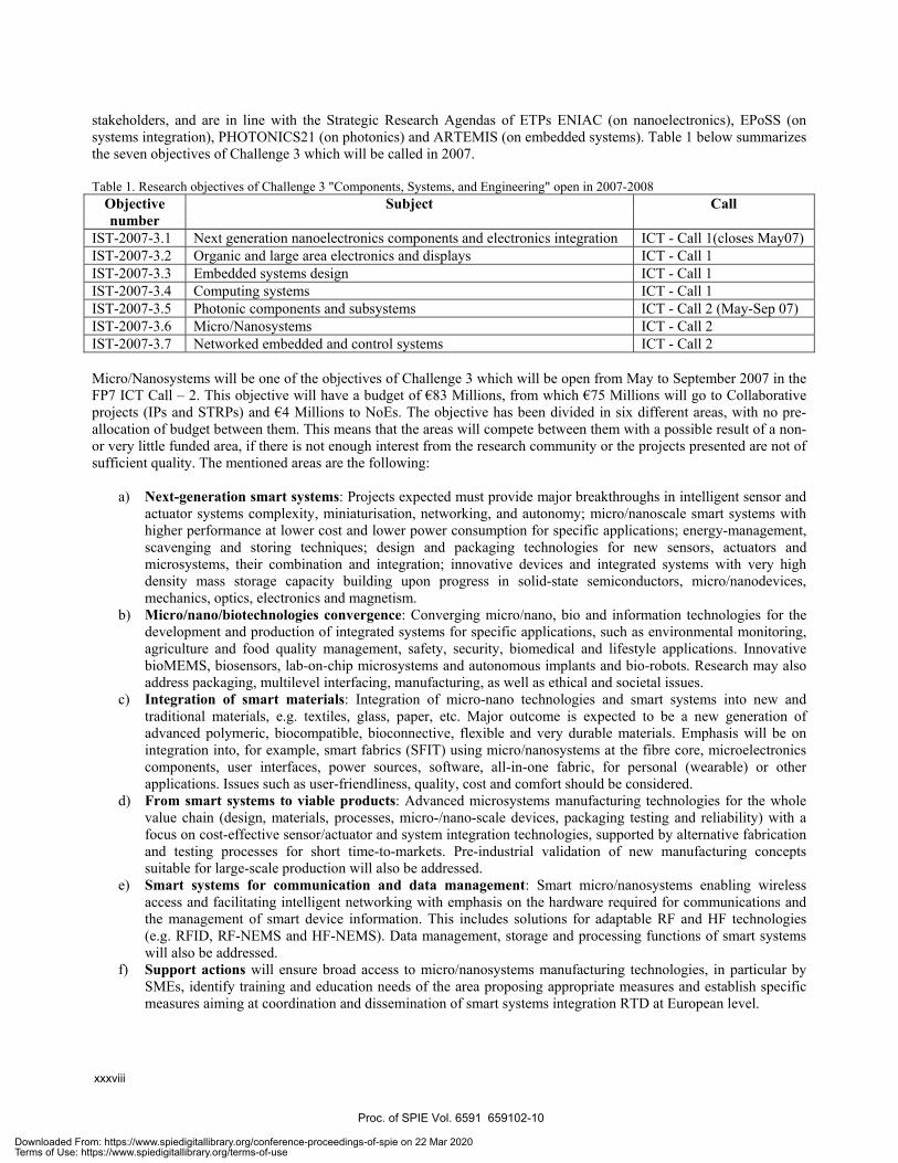
stakeholders, and are in line with the Strategic Research Agendas of ETPs ENIAC (on nanoelectronics), EPoSS (on systems integration), PHOTONICS21 (on photonics) and ARTEMIS (on embedded systems). Table 1 below summarizes the seven objectives of Challenge 3 which will be called in 2007. Table 1. Research objectives of Challenge 3 "Components, Systems, and Engineering" open in 2007-2008
Objective number
Subject Call
IST-2007-3.1 Next generation nanoelectronics components and electronics integration ICT - Call 1(closes May07) IST-2007-3.2 Organic and large area electronics and displays ICT - Call 1 IST-2007-3.3 Embedded systems design ICT - Call 1 IST-2007-3.4 Computing systems ICT - Call 1 IST-2007-3.5 Photonic components and subsystems ICT - Call 2 (May-Sep 07) IST-2007-3.6 Micro/Nanosystems ICT - Call 2 IST-2007-3.7 Networked embedded and control systems ICT - Call 2 Micro/Nanosystems will be one of the objectives of Challenge 3 which will be open from May to September 2007 in the FP7 ICT Call – 2. This objective will have a budget of €83 Millions, from which €75 Millions will go to Collaborative projects (IPs and STRPs) and €4 Millions to NoEs. The objective has been divided in six different areas, with no pre-allocation of budget between them. This means that the areas will compete between them with a possible result of a non-or very little funded area, if there is not enough interest from the research community or the projects presented are not of sufficient quality. The mentioned areas are the following:
a) Next-generation smart systems: Projects expected must provide major breakthroughs in intelligent sensor and actuator systems complexity, miniaturisation, networking, and autonomy; micro/nanoscale smart systems with higher performance at lower cost and lower power consumption for specific applications; energy-management, scavenging and storing techniques; design and packaging technologies for new sensors, actuators and microsystems, their combination and integration; innovative devices and integrated systems with very high density mass storage capacity building upon progress in solid-state semiconductors, micro/nanodevices, mechanics, optics, electronics and magnetism.
b) Micro/nano/biotechnologies convergence: Converging micro/nano, bio and information technologies for the development and production of integrated systems for specific applications, such as environmental monitoring, agriculture and food quality management, safety, security, biomedical and lifestyle applications. Innovative bioMEMS, biosensors, lab-on-chip microsystems and autonomous implants and bio-robots. Research may also address packaging, multilevel interfacing, manufacturing, as well as ethical and societal issues.
c) Integration of smart materials: Integration of micro-nano technologies and smart systems into new and traditional materials, e.g. textiles, glass, paper, etc. Major outcome is expected to be a new generation of advanced polymeric, biocompatible, bioconnective, flexible and very durable materials. Emphasis will be on integration into, for example, smart fabrics (SFIT) using micro/nanosystems at the fibre core, microelectronics components, user interfaces, power sources, software, all-in-one fabric, for personal (wearable) or other applications. Issues such as user-friendliness, quality, cost and comfort should be considered.
d) From smart systems to viable products: Advanced microsystems manufacturing technologies for the whole value chain (design, materials, processes, micro-/nano-scale devices, packaging testing and reliability) with a focus on cost-effective sensor/actuator and system integration technologies, supported by alternative fabrication and testing processes for short time-to-markets. Pre-industrial validation of new manufacturing concepts suitable for large-scale production will also be addressed.
e) Smart systems for communication and data management: Smart micro/nanosystems enabling wireless access and facilitating intelligent networking with emphasis on the hardware required for communications and the management of smart device information. This includes solutions for adaptable RF and HF technologies (e.g. RFID, RF-NEMS and HF-NEMS). Data management, storage and processing functions of smart systems will also be addressed.
f) Support actions will ensure broad access to micro/nanosystems manufacturing technologies, in particular by SMEs, identify training and education needs of the area proposing appropriate measures and establish specific measures aiming at coordination and dissemination of smart systems integration RTD at European level.
Proc. of SPIE Vol. 6591 659102-10
xxxviii
Downloaded From: https://www.spiedigitallibrary.org/conference-proceedings-of-spie on 22 Mar 2020Terms of Use: https://www.spiedigitallibrary.org/terms-of-use

The expected impact of the projects funded can be summarized as follow: • Substantial improvement on various aspects of smart systems integration: Higher product quality and reliability,
increased miniaturisation, integration and functionality, lower costs, reduced power consumption, higher speed requirements and/or shorter time-to market.
• Transformation of industrial production by adding intelligence to process control and the manufacturing shop floor, and by improving logistics and distribution - thereby increasing productivity.
• Increased market share for European companies across different industrial sectors by delivering systems with new functional capabilities and improved quality within a competitive timeframe.
As a summary, the area of micro and nanotechnologies and systems will be certainly well covered in the ICT Theme of FP7. Currently, the workprogramme for the years 2007 and 2008 has been published and the area has kept its interest and importance as in the previous FP6. The different objectives and areas which will be open in the coming FP7 workprogrammes will very much depend on the results of the first two ICT calls of proposals in 2007.
REFERENCES 1 European Communication "i2010 – A European Information Society for growth and employment". http://ec.europa.eu/information_society/eeurope/i2010/introduction/index_en.htm. 2 European Communication "i2010 – A European Information Society for growth and employment". http://ec.europa.eu/information_society/eeurope/i2010/introduction/index_en.htm. 3 DigiWorld2005. IDATE Foundation. ISBN: 2-84822-079-1 4 http://cordis.europa.eu/technology-platforms 5 Tecnologías Convergentes NBIC. Situación y Perspectiva. CSIC. ISBN:84-609-8230-0 6 http://www.csem.ch/sfit/ 7 Article 169: “In implementing the multi-annual framework programme, the Community may make provision, in agreement with the Member States concerned, for participation in research and development programmes undertaken by several Member States, including participation in the structures created for the execution of these programmes.” http://eur-lex.europa.eu/LexUriServ/site/es/oj/2006/ce321/ce32120061229es00010331.pdf 8 Article 171: “The Community may set up joint undertakings or any other structure necessary for the efficient execution of Community research, technological development and demonstration programmes. ” http://eur-lex.europa.eu/LexUriServ/site/es/oj/2006/ce321/ce32120061229es00010331.pdf
Proc. of SPIE Vol. 6591 659102-11
xxxix
Downloaded From: https://www.spiedigitallibrary.org/conference-proceedings-of-spie on 22 Mar 2020Terms of Use: https://www.spiedigitallibrary.org/terms-of-use

Downloaded From: https://www.spiedigitallibrary.org/conference-proceedings-of-spie on 22 Mar 2020Terms of Use: https://www.spiedigitallibrary.org/terms-of-use