power quality improvement by harmonic … · this to certify that the thesis report ... academic...
TRANSCRIPT

Page | 1
POWER QUALITY IMPROVEMENT BY HARMONIC REDUCTION USING
THREE PHASE SHUNT ACTIVE POWER FILTER WITH p-q & d-q
CURRENT CONTROL STRATEGY
DIBYENDU BHADRA (111EE0429) RAJNISH KUMAR MEENA (111EE0449)
Department of Electrical Engineering,
National Institute of Technology, Rourkela
Page | 2
POWER QUALITY IMPROVEMENT BY HARMONIC REDUCTION USING THREE
PHASE SHUNT ACTIVE POWER FILTER WITH p-q & d-q CURRENT CONTROL STRATEGY
A thesis submitted in partial fulfilment of the requirements for the degree of
Bachelor of Technology in “Electrical Engineering”
BY
DIBYENDU BHADRA RAJNISH KUMAR MEENA (111EE0429) (111EE0449)
Under the Supervision of
PROF. (MRS.) DIPTI PATRA
DEPT. OF ELECTRICAL ENGINEERING
NATIONAL INSTITUTE OF TECHNOLOGY, ROURKELA

Page | 3
NATIONAL INSTITUTE OF TECHNOLOGY, ROURKELA DEPARTMENT OF ELECTRICAL ENGINEERING
CERTIFICATE
This to certify that the thesis report entitled “POWER QUALITY IMPROVEMENT BY
HARMONIC REDUCTION USING THREE PHASE SHUNT ACTIVE POWER
FILTER WITH p-q & d-q CURRENT CONTROL STRATEGY” is a bona fide work
carried by DIBYENDU BHADRA, ROLL NO: 111EE0429, in partial fulfillment for the
award of Bachelor of Technology in Electrical Engineering at National Institute
of Technology, Rourkela during the year 2014-2015 under my supervision and guidance. The
thesis report has been approved as it satisfies the academic requirements in respect of Project
work prescribed for the said Degree. The thesis report which is based on candidate’s own work
has not been submitted elsewhere for a degree/diploma.
Place: Rourkela Prof. DIPTI PATRA Date: Supervisor
Department of Electrical Engineering National Institute of Technology Rourkela – 769 008 (ODISHA)

Page | 4
NATIONAL INSTITUTE OF TECHNOLOGY, ROURKELA DEPARTMENT OF ELECTRICAL ENGINEERING
CERTIFICATE
This to certify that the thesis report entitled “POWER QUALITY IMPROVEMENT BY
HARMONIC REDUCTION USING THREE PHASE SHUNT ACTIVE POWER
FILTER WITH p-q & d-q CURRENT CONTROL STRATEGY” is a bona fide work
carried by RAJNISH KUMAR MEENA, ROLL NO: 111EE0449, in partial fulfillment for
the award of Bachelor of Technology in Electrical Engineering at National
Institute of Technology, Rourkela during the year 2014-2015 under my supervision and
guidance. The thesis report has been approved as it satisfies the academic requirements in
respect of Project work prescribed for the said Degree. The thesis report which is based on
candidate’s own work has not been submitted elsewhere for a degree/diploma.
Place: Rourkela Prof. DIPTI PATRA Date: Supervisor
Department of Electrical Engineering National Institute of Technology Rourkela – 769 008 (ODISHA)

Page | 5
ACKNOWLEDGEMENTS
We would like express our deepest gratitude and profound appreciation to our project supervisor
Prof. Dipti Patra, for her patience, motivation, expert guidance and constructive suggestion for
fulfillment of our project work.
We would like to express our sincere thanks to Prof. A.K.Panda, Head of the Department,
Electrical Engineering for his invaluable suggestion and constant support throughout the project
work.
We also like to thank Prof. P.K.Roy, Prof. Gopalkrishna and other faculty members of Electrical
Engineering Department, NIT Rourkela for their encouragement, valuable guidance and
motivation.
We would like to acknowledge the entire teaching and non-teaching staff of Electrical department
for establishing a constructive working environment and guidance during lab work.
Further we like to appreciate all our friends whose valuable technical and non-technical suggestion
makes our project successful one.
Last but not the least; we would like to thank our parents, family and all well-wishers for their co-
operation, sacrifice and motivational moral support which bring us to this level.
DIBYENDU BHADRA RAJNISH KUMAR MEENA 111EE0429 111EE0449
Page | 6
TABLE OF CONTENTS
CERTIFICATE 3 ACKNOWLGEMENT 5 ABSTRACT 12 TABLE OF CONTENETS 6 LIST OF FIGURES 9 LIST OF TABLES 10 ABBREVIATIONS AND ACRONYMS 11
CHAPTER-1
INTRODUCTION
1.1. BACKGROUND 14 1.2. MOTIVATION OF PROJECT WORK 15 1.3. OBJECTIVES OF PROJECT WORK 15
CHAPTER-2
HARMONICS AND HARMONIC COMPENSATION SCHEMES
2.1. SOURCES OF HARMONICS 17 2.2. EFFECT OF HARMONICS 17 2.3. HARMONICS MITIGATION TECHNIQUES 18 2.3.1. PASSIVE FILTER 18 2.3.1.1. ADVANTAGES OF PASSIVE FILTER 19 2.3.1.2. DISADVANTAGES OF PASSIVE FILTER 19 2.3.2. ACTIVE POWER FILTER 20 2.3.2.1. OPERATION OF ACTIVE FILTER 20 2.3.2.2. ADVANTAGES OF ACTIVE FILTER 21
Page | 7
CHAPTER-3
LITERATURE REVIEW
3.1. SHUNT ACTIVE POWER FILTER 23 3.2. INSTANTANEOUS REAL AND REACTIVE POWER THEORY (P-Q METHOD) 24 3.3. HYSTERESIS CURRENT CONTROLLER 25 3.4. SYNCHRONOUS REFERENCE FRAME THEORY (D-Q METHOD) 27
CHAPTER-4
MATHEMATICAL MODELLING
4.1. P-Q METHOD MATHEMATICAL MODELLING 29 4.2. D-Q METHOD MATHEMATICAL MODELLING 30
CHAPTER-5
MATLAB MODELLING AND DESIGN SPECIFICATION
5.1. POWER SYSTEM SIMULINK MODEL WITH SHUNT APF & NON LINEAR LOAD 32 5.2. SIMULINK MODEL WITH SHUNT APF WITH P-Q METHOD 32 5.3. SIMULINK MODEL WITH SHUNT APF WITH D-Q METHOD 33 5.4. DESIGN PARAMETERS FOR MATLAB SIMULATION 33
CHAPTER-6
SIMULATION RESULT AND COMPARISON
6.1. SIMULINK RESULT 35 6.1.1. SIMULATION RESULT WITH P-Q CONTROL STRATEGY 35 6.1.2. SIMULATION RESULT WITH D-Q CONTROL STRATEGY 37 6.2. FFT ANALYSIS 39 6.3. COMPARATIVE ANALYSIS 41 6.4. GRAPHICAL COMPARISION 42
Page | 8
CHAPTER-7
COMPONENT DESCRIPTION
7.1. INTRODUCTION 45 7.1.1. SINGLE PHASE VARIAC 45 7.1.2. IGBT BASED INVERTER 45 7.1.3. THREE PHASE BRIDGE RECTIFIER 45 7.1.4. SIGNAL CONDITIONING 46 7.1.4.1. CURRENT SENSOR 46 7.1.4.2. VOLTAGE SENSOR 48 7.1.4.3. GATE DRIVER 49 7.1.5. FILTER INDUCTOR 50 7.1.6. DC LINK CAPACITOR 51 7.1.7. R-L LOAD 51
CHAPTER-8
CONCLUSION 8.1. CONCLUSION AND FUTURE ACTIVITY 53 REFERENCES 54 APPENDIX-A 55 APPENDIX-B 56 APPENDIX-C 57 APPENDIX-D 58
Page | 9
LIST OF FIGURES
1. SHUNT ACTIVE POWER FILTER 23
2. P-Q METHOD CONTROL STRATEGY 24
3. HYSTERESIS CONTROLLER CONTROL LOGIC 25
4. HYSTERESIS BAND 26
5. D-Q METHOD CONTROL STRATEGY 27
6. SYSTEM MODEL WITH FILTER 32
7. MODEL OF SHUNT APF WITH P-Q METHOD 32
8. MODEL OF SHUNT APF WITH D-Q METHOD 33
9.1. SOURCE VOLTAGE WAVEFORM BEFORE & AFTER FILTERING WITH P-Q METHOD 35
9.2 SOURCE CURRENT WAVEFORM BEFORE & AFTER FILTERING WITH P-Q METHOD 35
9.3. LOAD VOLTAGE WAVEFORM BEFORE & AFTER FILTERING WITH P-Q METHOD 36
9.4. LOAD CURRENT WAVEFORM BEFORE & AFTER FILTERING WITH P-Q METHOD 36
9.5. APF CURRENT WAVEFORM BEFORE & AFTER FILTERING WITH P-Q METHOD 36
9.6. DC LINK VOLTAGE WAVEFORM BEFORE & AFTER FILTERING WITH P-Q METHOD 36
9.7. COMPENSATING CURRENT WAVEFORM 37
9.8. ACTIVE POWER WAVEFORM 37
9.9. REACTIVE POWER WAVEFORM 37
10.1. SOURCE VOLTAGE WAVEFORM BEFORE & AFTER FILTERING WITH D-Q METHOD 37
10.2. SOURCE CURRENT WAVEFORM BEFORE & AFTER FILTERING WITH D-Q METHOD 37
10.3. LOAD VOLTAGE WAVEFORM BEFORE & AFTER FILTERING WITH D-Q METHOD 38
10.4. LOAD CURRENT WAVEFORM BEFORE & AFTER FILTERING WITH D-Q METHOD 38
10.5. APF CURRENT WAVEFORM BEFORE & AFTER FILTERING WITH D-Q METHOD 38
10.6. COMPENSATING CURRENT WAVEFORM 38
Page | 10
10.7. DC LINK VOLTAGE WAVEFORM BEFORE & AFTER FILTERING WITH D-Q METHOD 39
11.1. FFT ANALYSIS OF SOURCE WITHOUT SAPF 39
11.2. FFT ANALYSIS OF SOURCE CURRENT WITH APF USING P-Q METHOD 40
11.3. FFT ANALYSIS OF SOURCE CURRENT WITH APF USING D-Q METHOD 40
12.1. COMPARATIVE GRAPH BETWEEN SYSTEM WITHOUT AND WITH SAPF 42
12.2. COMPARATIVE GRAPH BETWEEN P-Q AND D-Q METHOD 43
13.1. WORKING PRINCIPLE OF CURRENT SENSOR 46
13.2. LA 55-P CURRENT SENSOR 46
14.1. WORKING PRINCIPLE OF VOLTAGE SENSOR 48
14.2. LV 25-P VOLTAGE SENSOR 48
15.1. WORKING PRINCIPLE OF GATE DRIVER CIRCUIT 50
15.2. GATE DRIVER CIRCUIT 50
16. DC LINK CAPACITOR 51
17. R-L LOAD 51
LIST OF TABLES
1. SYSTEM PARAMETERS SPECIFICATION 33
2. SAPF PARAMETERS SPECIFICATION 33
3. HARMONIC COMPONENT AS % OF FUNDAMENTAL FREQUENCY COMPONENT 41
4. TOTAL HARMONIC DISTORTION OF SYSTEM WITH AND WITHOUT FILTER 41
Page | 11
ABBREVIATIONS AND ACRONYMS
SCR – Silicon Controlled Rectifier
IGBT – Insulated Gate Bipolar Transistor
MOSFET – Metal Oxide Semiconductor Field Effect Transistor
APF – Active Power Filter
PCC – Point of Common Coupling
SMPS – Switched Mode Power Supply
UPS – Uninterruptible Power Supply
AC – Alternating Current
DC – Direct Current
THD – Total Harmonic Distortion
PWM – Pulse Width Modulation
VSI – Voltage Source Inverter
SAPF – Shunt Active Power Filter
FFT – Fast Fourier Transform
DSP – Digital Signal Processing
PLL – Phase Locked Loop
LPF – Low Pass Filter
ADC – Analog to Digital Converter
IC – Integrated Circuit
Page | 12
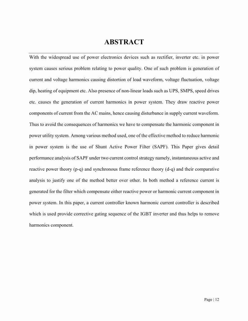
ABSTRACT
With the widespread use of power electronics devices such as rectifier, inverter etc. in power
system causes serious problem relating to power quality. One of such problem is generation of
current and voltage harmonics causing distortion of load waveform, voltage fluctuation, voltage
dip, heating of equipment etc. Also presence of non-linear loads such as UPS, SMPS, speed drives
etc. causes the generation of current harmonics in power system. They draw reactive power
components of current from the AC mains, hence causing disturbance in supply current waveform.
Thus to avoid the consequences of harmonics we have to compensate the harmonic component in
power utility system. Among various method used, one of the effective method to reduce harmonic
in power system is the use of Shunt Active Power Filter (SAPF). This Paper gives detail
performance analysis of SAPF under two current control strategy namely, instantaneous active and
reactive power theory (p-q) and synchronous frame reference theory (d-q) and their comparative
analysis to justify one of the method better over other. In both method a reference current is
generated for the filter which compensate either reactive power or harmonic current component in
power system. In this paper, a current controller known harmonic current controller is described
which is used provide corrective gating sequence of the IGBT inverter and thus helps to remove
harmonics component.

Page | 13
CHAPTER 1
INTRODUCTION
Page | 14
1.1 Background
Power electronic switching device in conjunction with nonlinear loads causes serious harmonic
problem in power system due to their inherent property of drawing harmonic current and reactive
power from AC supply mains. They cause voltage unbalance and neutral currents problem in
power system. With the distortion of current and voltage waveform due to presence of harmonic
effect the power system equipment that are connected to maintain steady and reliable power flow
in the power system. Major effects include overheating, capacitor failure, vibration, resonance
problem, low power factor, overloading, communication interference and power fluctuation. Thus
to improve the performance it is required to eliminate harmonics from power utility system [1].
One of the method used for elimination is the use of shunt active power filter (SAPF) in which a
reference current is generated to remove distortion from the harmonic currents. Shunt active power
filter continuously monitor the harmonics current and reactive power flow in the network and
generate reference current from distorted current waveform. Thus dynamic closed loop action of
SAPF helps the reduction of harmonics and compensation of reactive power in real time basis with
little time delay. SAPF can be used with different current control strategy such as d-q method,
fuzzy logic controller, p-q method, neural networks etc. which is helpful in removing effective
harmonic from power system.
Page | 15
1.2 Motivation of Project Work
Harmonic pollution is mostly common in low voltage side due to wide use of nonlinear loads
(UPS, SMPS, Rectifier etc.), which is undesirable as it cause serious voltage fluctuation and
voltage dip in power system. So it required to eliminate undesirable current and voltage harmonics
and to compensate the reactive power to improve the performance and operation of the power
system. The use of traditional passive filter in removing harmonics is not that much effective
because their static action and no real time action or dynamic action is taken for the removal of
harmonics. But the shunt active power filter on the other hand gives promising results when
compared with conventional active and passive filters. This project basically shows the comparison
between two current control strategy [8] i.e. synchronous frame reference method and
instantaneous active-reactive power method which is helpful to reduce the current harmonics when
used with SAPF through MATLAB simulation and modeling.
1.3 Objectives of Project Work
The main objectives of this project are
To give a brief overview about the cause and effect of harmonics in power system
To study different types proposed filter used to eliminate harmonics from the power
system.
To study and implement different control strategies already proposed for modeling of 3
phase shunt active power filter
To model and simulate three phase shunt active power filter with different current control
strategy in MATLAB/SIMULINK environment
To compare different control strategies based on FFT analysis (an important tool for
harmonic behavioral analysis) for harmonic elimination in power system network.

Page | 16
CHAPTER 2
HARMONICS AND
HARMONIC
COMPENSATION
SCHEMES
Page | 17
2.1 Source of Harmonics
Harmonics are usually defined as periodic steady state distortions or deterioration of original
voltage and/or current waveforms in power systems where frequency of harmonic wave is an
integral multiple of fundamental frequency. Major sources of voltage and current harmonic
generation in power system are
Controlling action of power electronic devices such as chopper, inverter etc. cause
imbalance in power system leading to harmonic generation.
Non-linear load such as UPS, SMPS, battery charger.
Power electronic converter such as high-voltage direct-current power converters, traction
and power converters, wind and solar-powered dc/ac converters etc. [5] cause harmonic
generation owing to their energy conversion and controlling action.
Heating material in ac/dc converters acts as a nonlinear load whose controlling action
produces harmonics [5] due to inherent property of high reactive power requirement.
2.2 Effect of Harmonics
Harmonics may cause interference and disturbance in power systems network. Some of the major
problems include:
Harmonic currents present in the power system causes heating of equipment, such as
transformers and generators and give huge copper loss.
In generators owing to multiple zero crossings of distorted current waveform causes
voltage instability and voltage fluctuation.
Since frequency of harmonic current is different from that of fundamental may cause
improper breaker and switch operation which is undesirable.
Page | 18
2.3 Harmonic Mitigation Techniques
Harmonic elimination techniques are used to improve the power system performance with some
objectives
To improve the system power factor and to compensate the reactive power.
To maintain a particular THD limit in current harmonic distribution.
Hence various devices and equipment serves the purpose of harmonic elimination from power
system. Some of widely used equipment are:
1) Line reactors (Inductive reactor)
2) Isolation transformers (provide isolation of high power circuit from low power circuit)
3) K-Factor or harmonic mitigating transformers
4) Phase shifting transformer
5) Harmonic filters
But mostly current harmonic filters are used to reduce current harmonics in power system. There
are generally two types of harmonic filters are present: i) passive filter and ii) active filters.
2.3.1 Passive Filter It is a combination of series/parallel connection of passive elements such as capacitors, inductors
and/or resistor. They provide a low resistance path for the harmonic current to flow owing to the
formation of resonance at that particular harmonic frequency. Hence harmonic current is diverted
through passive filter network and system current becomes distortion free. Likewise distortion in
voltage waveform is also removed. For bypassing the current effective means of connection is
connecting the passive filter in parallel with the load. In order to improve power factor passive
filters are designed as capacitive filter so that it correct the current displacement factor and provide
reactive power to the load.

Page | 19
Different variety of passive filters such as single tuned, double tuned, high pass and c-type filters
are used for harmonic mitigation purpose but among them most commonly used filter is single
tuned filter. It comprises of series combination of inductor and capacitor which provide low
impedance for tuned harmonics while resonating at tuning frequency.
2.3.1.1 Advantages of Passive Filters
Although passive filters doesn’t eliminate harmonics to a greater extent yet it is used due to some
prominent features which are described as under
1. They are simpler to configure and construct.
2. Low initial & maintenance cost (compared to APF)
3. Shunt passive filters of capacitive nature provide reactive power to the nonlinear load and
on the other hand improve power factor by improving current displacement factor.
4. Lowering of THD in line current to a permissible limit can be possible by use of passive
filter.
2.3.1.2 Disadvantages of Passive Filters
Some major drawbacks with passive current filters are:
1. Property and characteristics of filter depends on source impedance (i.e. impedance of the
system and its topology) which are subjected to variations due to external condition.
2. Resonating condition in the filter may create problem with loads and network leading to
voltage fluctuation.
3. It basically able to remove some particular harmonic components through tuning whenever
the magnitude of those harmonic component is constant and pf of the system is low.
4. Filter response is static i.e. if load variation introduce some new harmonic components then
the filter have to redesigned which increases the maintenance and operation cost of the
Page | 20
filter.
5. Load unbalancing or neutral shifting problems can’t be solved.
2.3.2 Active Filter An active filter consists of serial/parallel array of arrangement of both active and passive
components and it is a type of analog electronic filter. Basic building block of active filter are
Amplifiers. Thus filter performance and response is improved by the use of amplifiers instead of
inductors that are used in passive filter for the same purpose. Active filter have dynamic response
and thus can remove current distortion, current harmonics etc. faster than passive filter. It can also
be used for reactive power compensation and also for voltage based distortions such as flickering,
voltage dip, unbalancing. It uses PWM techniques to remove load unbalancing and neutral shifting
problems. There is no possibility of resonating condition as tuning of frequency isn’t taking place
in active filtering, so the power system network remain more stable during operation. Unlike
passive filter, there performance doesn’t depends on system parameters and its topology.
2.3.2.1 Operation of Active Filters
Active Filter generate compensating current signal by continuously monitoring the load current
with the help of some algorithm such as p-q theory, d-q transform, sliding mode control, DSP
based algorithm etc. Now the generated compensating current is used to generate the switching
pulse and switching sequence of IGBT inverter with the help of hysteresis controller or any other
type of current controller. The inverter then generate the required harmonic current for the load
through charging and discharging of DC link capacitor and injected into the system through
coupling transformer with a phase difference to compensate the reactive power coming from the
AC mains.
Major types of Active filters are: i) Series AF, ii) Shunt AF and iii) Hybrid AF.
Page | 21
2.3.2.2 Advantages of Active Filters
1. Widely compensated the THD in source current waveform.
2. Only a single filter can be able to eliminate all the unwanted harmonics.
3. Resonance condition is absent which increase the stability of power system.
4. Filter characteristics changes with load variation due to dynamic response of the filter.

Page | 22
CHAPTER-3
LITERATURE REVIEW
Page | 23
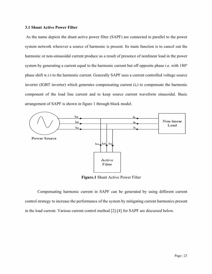
3.1 Shunt Active Power Filter
As the name depicts the shunt active power filter (SAPF) are connected in parallel to the power
system network wherever a source of harmonic is present. Its main function is to cancel out the
harmonic or non-sinusoidal current produce as a result of presence of nonlinear load in the power
system by generating a current equal to the harmonic current but off opposite phase i.e. with 180ο
phase shift w.r.t to the harmonic current. Generally SAPF uses a current controlled voltage source
inverter (IGBT inverter) which generates compensating current (ic) to compensate the harmonic
component of the load line current and to keep source current waveform sinusoidal. Basic
arrangement of SAPF is shown in figure 1 through block model.
Figure.1 Shunt Active Power Filter
Compensating harmonic current in SAPF can be generated by using different current
control strategy to increase the performance of the system by mitigating current harmonics present
in the load current. Various current control method [2]-[4] for SAPF are discussed below.
Page | 24
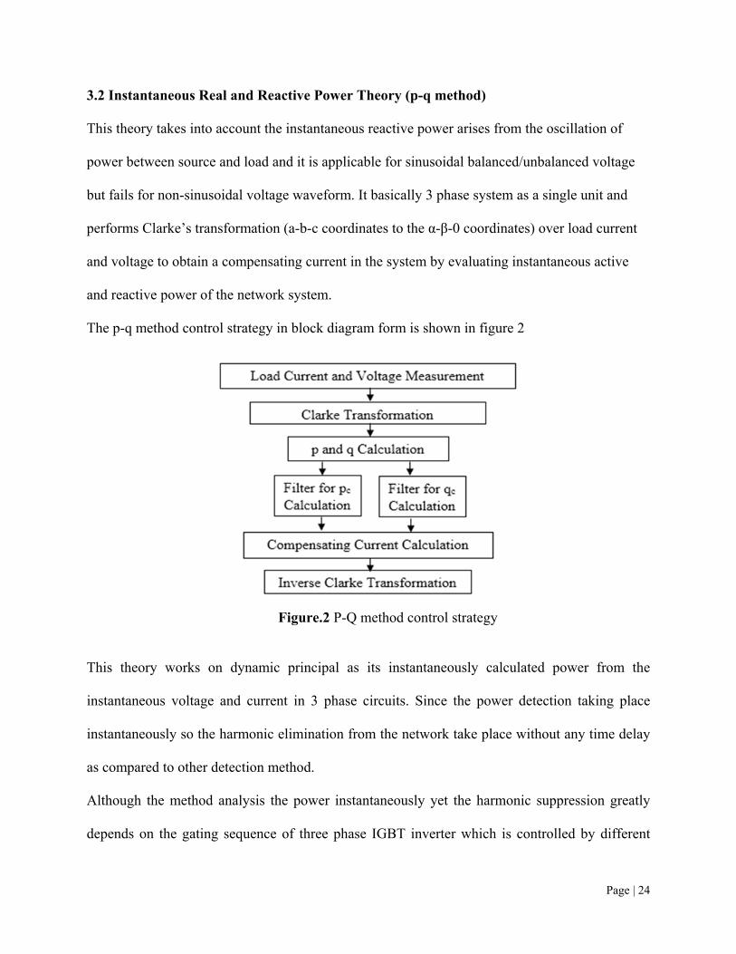
3.2 Instantaneous Real and Reactive Power Theory (p-q method)
This theory takes into account the instantaneous reactive power arises from the oscillation of
power between source and load and it is applicable for sinusoidal balanced/unbalanced voltage
but fails for non-sinusoidal voltage waveform. It basically 3 phase system as a single unit and
performs Clarke’s transformation (a-b-c coordinates to the α-β-0 coordinates) over load current
and voltage to obtain a compensating current in the system by evaluating instantaneous active
and reactive power of the network system.
The p-q method control strategy in block diagram form is shown in figure 2
Figure.2 P-Q method control strategy
This theory works on dynamic principal as its instantaneously calculated power from the
instantaneous voltage and current in 3 phase circuits. Since the power detection taking place
instantaneously so the harmonic elimination from the network take place without any time delay
as compared to other detection method.
Although the method analysis the power instantaneously yet the harmonic suppression greatly
depends on the gating sequence of three phase IGBT inverter which is controlled by different
Page | 25
current controller such as hysteresis controller, PWM controller, triangular carrier current
controller. But among these hysteresis current controlled method is widely used due to its
robustness, better accuracy and performance which give stability to power system.
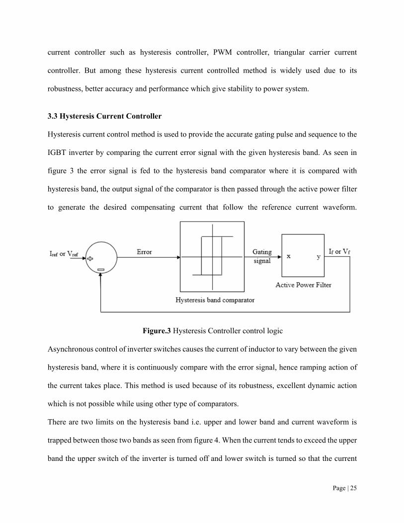
3.3 Hysteresis Current Controller
Hysteresis current control method is used to provide the accurate gating pulse and sequence to the
IGBT inverter by comparing the current error signal with the given hysteresis band. As seen in
figure 3 the error signal is fed to the hysteresis band comparator where it is compared with
hysteresis band, the output signal of the comparator is then passed through the active power filter
to generate the desired compensating current that follow the reference current waveform.
Figure.3 Hysteresis Controller control logic
Asynchronous control of inverter switches causes the current of inductor to vary between the given
hysteresis band, where it is continuously compare with the error signal, hence ramping action of
the current takes place. This method is used because of its robustness, excellent dynamic action
which is not possible while using other type of comparators.
There are two limits on the hysteresis band i.e. upper and lower band and current waveform is
trapped between those two bands as seen from figure 4. When the current tends to exceed the upper
band the upper switch of the inverter is turned off and lower switch is turned so that the current
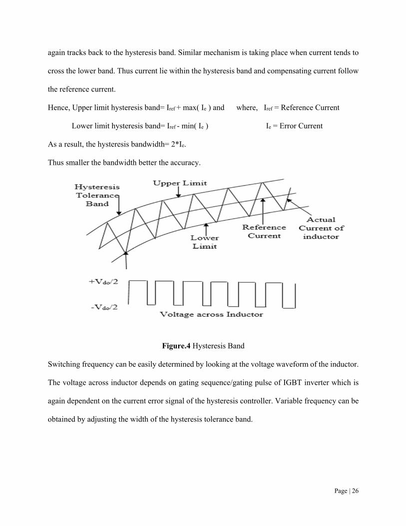
Page | 26
again tracks back to the hysteresis band. Similar mechanism is taking place when current tends to
cross the lower band. Thus current lie within the hysteresis band and compensating current follow
the reference current.
Hence, Upper limit hysteresis band= Iref + max( Ie ) and where, Iref = Reference Current
Lower limit hysteresis band= Iref - min( Ie ) Ie = Error Current
As a result, the hysteresis bandwidth= 2*Ie.
Thus smaller the bandwidth better the accuracy.
Figure.4 Hysteresis Band
Switching frequency can be easily determined by looking at the voltage waveform of the inductor.
The voltage across inductor depends on gating sequence/gating pulse of IGBT inverter which is
again dependent on the current error signal of the hysteresis controller. Variable frequency can be
obtained by adjusting the width of the hysteresis tolerance band.
Page | 27
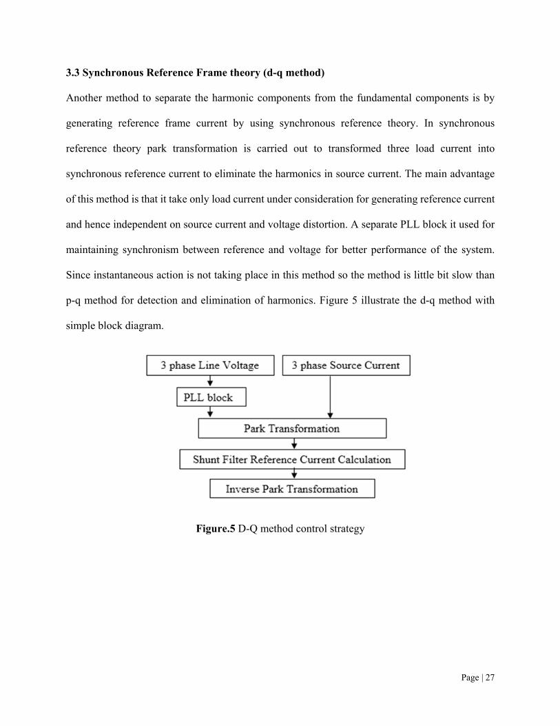
3.3 Synchronous Reference Frame theory (d-q method)
Another method to separate the harmonic components from the fundamental components is by
generating reference frame current by using synchronous reference theory. In synchronous
reference theory park transformation is carried out to transformed three load current into
synchronous reference current to eliminate the harmonics in source current. The main advantage
of this method is that it take only load current under consideration for generating reference current
and hence independent on source current and voltage distortion. A separate PLL block it used for
maintaining synchronism between reference and voltage for better performance of the system.
Since instantaneous action is not taking place in this method so the method is little bit slow than
p-q method for detection and elimination of harmonics. Figure 5 illustrate the d-q method with
simple block diagram.
Figure.5 D-Q method control strategy

Page | 28
CHAPTER-4
MATHEMATICAL
MODELLING
Page | 29
4.1 P-Q method Mathematical modelling
The relation between load current & voltage of three phase power system and the orthogonal
coordinates (α-β-0) system are expressed by Clarke’s transformation which is shown by the
following equations 1 & 2.
1
0√ √
………. (1)
1
0√ √
………. (2)
In orthogonal co-ordinate system instantaneous power can be found out by simply multiplying
the instantaneous current with their corresponding instantaneous voltage. Here the 3 phase co-
ordinate system (a-b-c) is mutually orthogonal is nature, so we can found out instantaneous
power as in the form of equation 3.
……….. (3)
From above equations, the instantaneous active and reactive power in matrix form can be
rewritten as
= ………… (4)
The instantaneous reactive power produces an opposing vector with 180ο phase shift in order to
cancel the harmonic component in the line current. From the above equations, yield equation 5.
∗
∗ =0
……. (5)
After finding the α-β reference current, the compensating current for each phase can be derived by
using the inverse Clarke transformations as shown in equation 6.
Page | 30
∗
∗
∗
1 0√
√
……… (6)
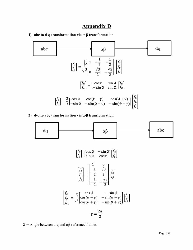
4.2 D-Q method Mathematical modelling According to Park’s transformation relation between three phase source current (a-b-c) and the
d-q reference co-ordinate current is given by equation 7
cos μ cos μ cos μ
sin μ sin μ sin μ
√ √ √
………. (7)
Where, ‘µ’ is the angular deviation of the synchronous reference frame from the 3 phase
orthogonal system which is a linear function of fundamental frequency. The harmonic reference
current can be obtained from the load currents using a simple LPF. The currents in the synchronous
reference system can be decomposed into two components given by equation 8 & 9
~ ……. (8)
~ …….. (9)
After filtering DC terms ( , ) are suppressed and alternating term are appearing in the output
of extraction system which are responsible for harmonic pollution in power system. The APF
reference currents is given by equation 10
∗
∗
~
~ ……. (10)
In order to find the filter currents in three phase system which cancels the harmonic components
in line side, the inverse Park transform can be used as shown by equation 11
∗
∗
∗
cos μ sin μ
cos μ sin μ
cos μ sin μ
∗
∗ ………… (11)

Page | 31
CHAPTER-5
MATLAB/SIMULINK
MODELLING
Page | 32
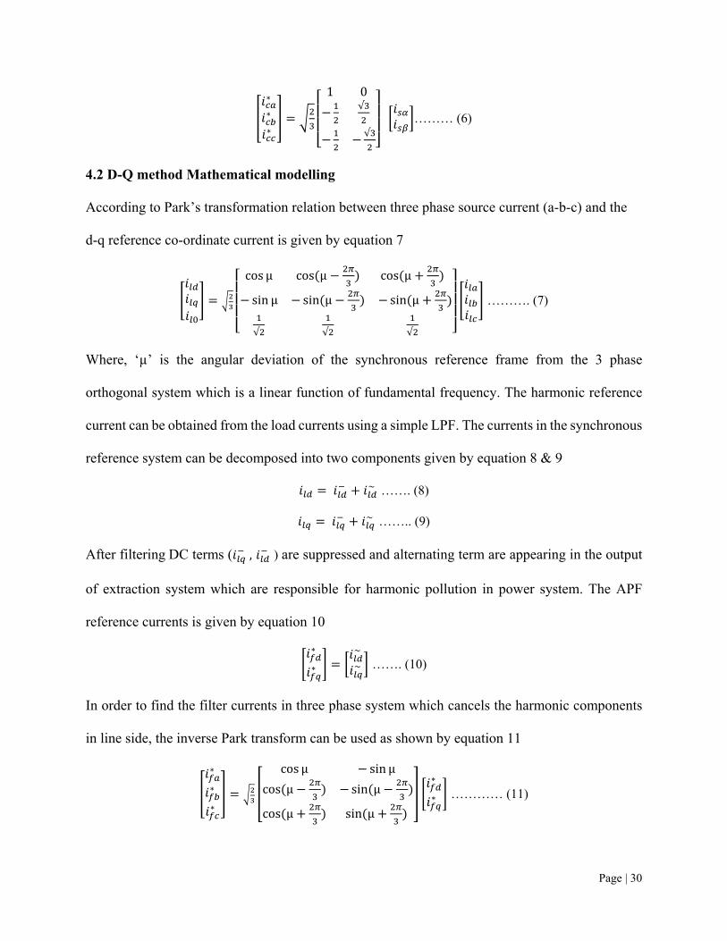
5.1 Power system Simulink model with Shunt APF and Non-linear load
Figure. 6 System model with filter
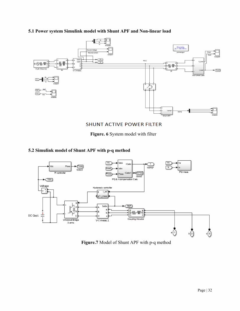
5.2 Simulink model of Shunt APF with p-q method
Figure.7 Model of Shunt APF with p-q method
Page | 33
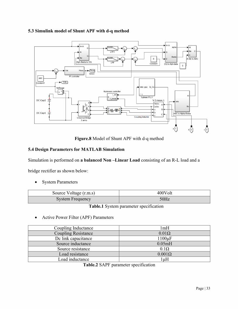
5.3 Simulink model of Shunt APF with d-q method
Figure.8 Model of Shunt APF with d-q method
5.4 Design Parameters for MATLAB Simulation
Simulation is performed on a balanced Non –Linear Load consisting of an R-L load and a
bridge rectifier as shown below:
System Parameters
Source Voltage (r.m.s) 400Volt System Frequency 50Hz
Table.1 System parameter specification
Active Power Filter (APF) Parameters
Coupling Inductance 1mH Coupling Resistance 0.01Ω Dc link capacitance 1100μF Source inductance 0.05mH Source resistance 0.1Ω Load resistance 0.001Ω Load inductance 1μH
Table.2 SAPF parameter specification
Page | 34
CHAPTER-6
SIMULATION RESULT
AND COMPARISON
Page | 35
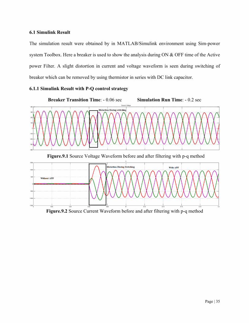
6.1 Simulink Result
The simulation result were obtained by in MATLAB/Simulink environment using Sim-power
system Toolbox. Here a breaker is used to show the analysis during ON & OFF time of the Active
power Filter. A slight distortion in current and voltage waveform is seen during switching of
breaker which can be removed by using thermistor in series with DC link capacitor.
6.1.1 Simulink Result with P-Q control strategy
Breaker Transition Time: - 0.06 sec Simulation Run Time: - 0.2 sec
Figure.9.1 Source Voltage Waveform before and after filtering with p-q method
Figure.9.2 Source Current Waveform before and after filtering with p-q method
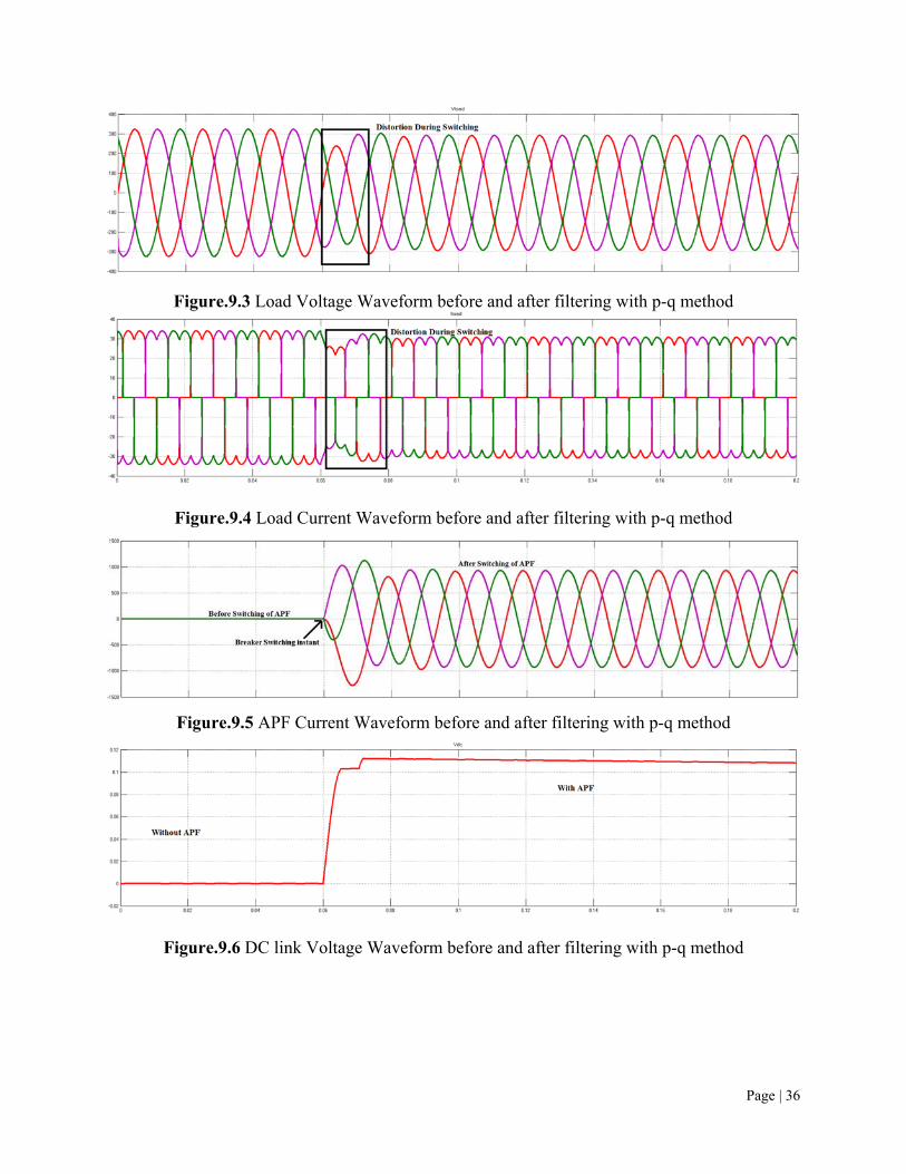
Page | 36
Figure.9.3 Load Voltage Waveform before and after filtering with p-q method
Figure.9.4 Load Current Waveform before and after filtering with p-q method
Figure.9.5 APF Current Waveform before and after filtering with p-q method
Figure.9.6 DC link Voltage Waveform before and after filtering with p-q method
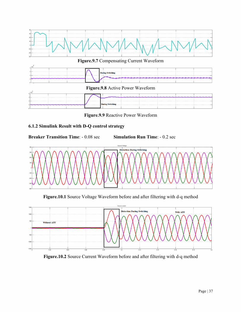
Page | 37
Figure.9.7 Compensating Current Waveform
Figure.9.8 Active Power Waveform
Figure.9.9 Reactive Power Waveform
6.1.2 Simulink Result with D-Q control strategy
Breaker Transition Time: - 0.08 sec Simulation Run Time: - 0.2 sec
Figure.10.1 Source Voltage Waveform before and after filtering with d-q method
Figure.10.2 Source Current Waveform before and after filtering with d-q method
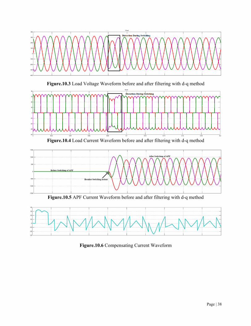
Page | 38
Figure.10.3 Load Voltage Waveform before and after filtering with d-q method
Figure.10.4 Load Current Waveform before and after filtering with d-q method
Figure.10.5 APF Current Waveform before and after filtering with d-q method
Figure.10.6 Compensating Current Waveform
Page | 39
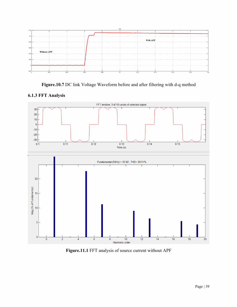
Figure.10.7 DC link Voltage Waveform before and after filtering with d-q method
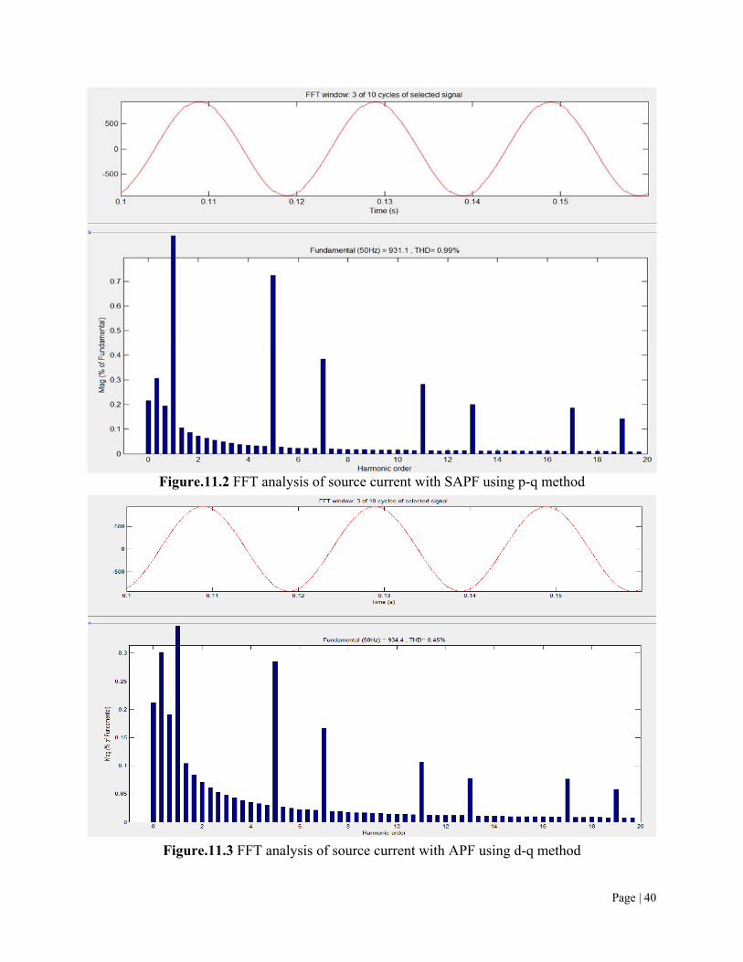
6.1.3 FFT Analysis
Figure.11.1 FFT analysis of source current without APF
Page | 40
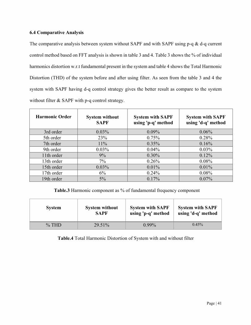
Figure.11.2 FFT analysis of source current with SAPF using p-q method
Figure.11.3 FFT analysis of source current with APF using d-q method
Page | 41
6.4 Comparative Analysis
The comparative analysis between system without SAPF and with SAPF using p-q & d-q current
control method based on FFT analysis is shown in table 3 and 4. Table 3 shows the % of individual
harmonics distortion w.r.t fundamental present in the system and table 4 shows the Total Harmonic
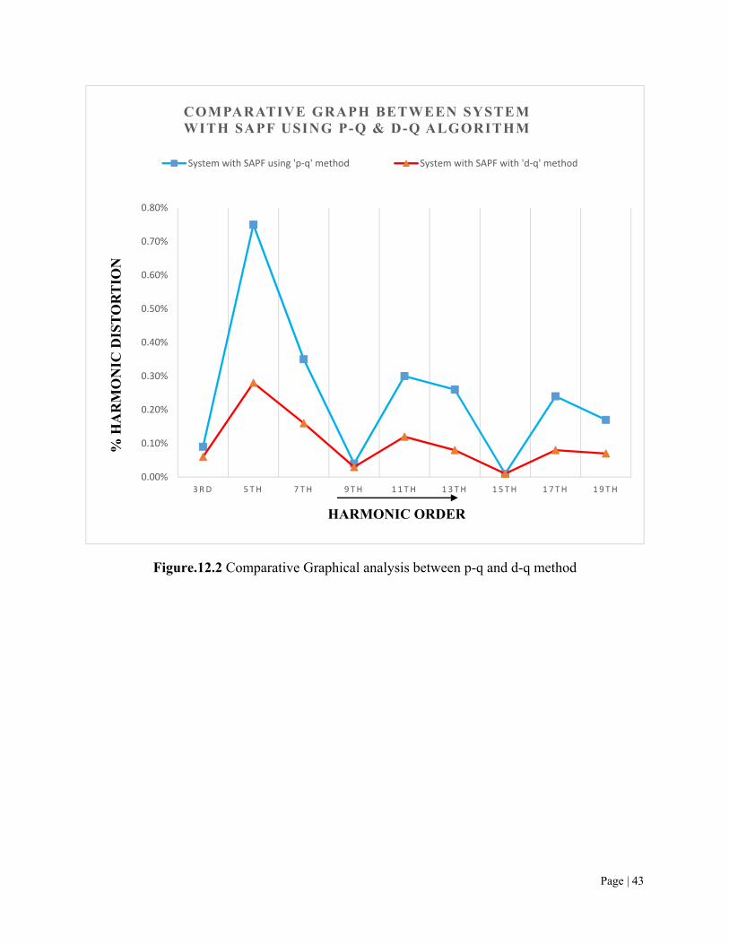
Distortion (THD) of the system before and after using filter. As seen from the table 3 and 4 the
system with SAPF having d-q control strategy gives the better result as compare to the system
without filter & SAPF with p-q control strategy.
Harmonic Order
System without SAPF
System with SAPF using 'p-q' method
System with SAPF using 'd-q' method
3rd order 0.03% 0.09% 0.06% 5th order 23% 0.75% 0.28% 7th order 11% 0.35% 0.16% 9th order 0.03% 0.04% 0.03%
11th order 9% 0.30% 0.12% 13th order 7% 0.26% 0.08% 15th order 0.03% 0.01% 0.01% 17th order 6% 0.24% 0.08%
19th order 5% 0.17% 0.07%
Table.3 Harmonic component as % of fundamental frequency component
System
System without
SAPF
System with SAPF using 'p-q' method
System with SAPF using 'd-q' method
% THD 29.51% 0.99% 0.45%
Table.4 Total Harmonic Distortion of System with and without filter
Page | 42
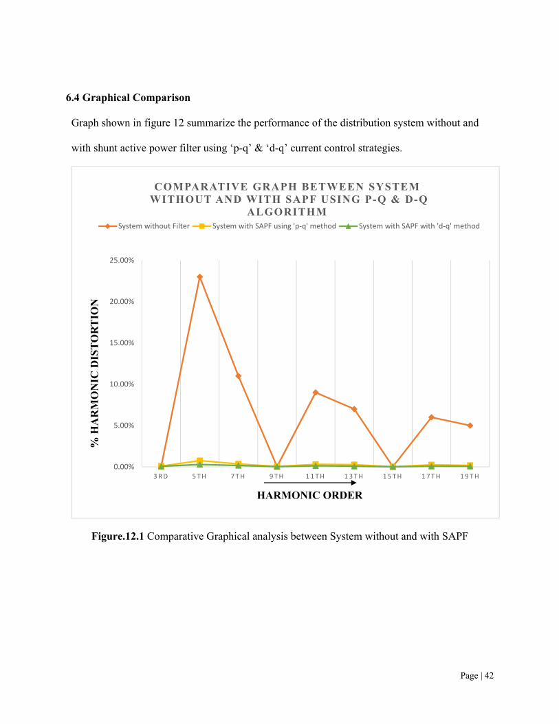
6.4 Graphical Comparison
Graph shown in figure 12 summarize the performance of the distribution system without and
with shunt active power filter using ‘p-q’ & ‘d-q’ current control strategies.
Figure.12.1 Comparative Graphical analysis between System without and with SAPF
0.00%
5.00%
10.00%
15.00%
20.00%
25.00%
3RD 5TH 7TH 9TH 11TH 13TH 15TH 17TH 19TH
% H
AR
MO
NIC
DIS
TO
RT
ION
HARMONIC ORDER
COMPARATIVE GRAPH BETWEEN SYSTEMWITHOUT AND WITH SAPF USING P-Q & D-Q
ALGORITHMSystem without Filter System with SAPF using 'p‐q' method System with SAPF with 'd‐q' method
Page | 43
Figure.12.2 Comparative Graphical analysis between p-q and d-q method
0.00%
0.10%
0.20%
0.30%
0.40%
0.50%
0.60%
0.70%
0.80%
3RD 5TH 7TH 9TH 11TH 13TH 15TH 17TH 19TH
% H
AR
MO
NIC
DIS
TO
RT
ION
HARMONIC ORDER
COMPARATIVE GRAPH BETWEEN SYSTEMWITH SAPF USING P-Q & D-Q ALGORITHM
System with SAPF using 'p‐q' method System with SAPF with 'd‐q' method
Page | 44
CHAPTER-7
COMPONENT
DESCRIPTION

Page | 45
7.1 INTRODUCTION
This chapter gives a brief idea about different components required to establish the experimental
set up. The different hardware requirements for experimental purpose are broadly classified into
1. Single phase Variac
2. 3 phase IGBT based inverter
3. Three phase bridge rectifier
4. Signal conditioning circuit
5. Filter inductor
6. DC link capacitor
7. R-L load
7.1.1 Single Phase Variac
It was used to provide control supplied voltage of 230 r.m.s Voltage between a phase and neutral
to start the experiment
7.1.2 IGBT Based Inverter
Six IGBT are used to provide the switching phenomena in a voltage source inverter so that
controlled DC voltage is obtained across the DC link capacitor. IGBT to be used are of
SEMIKRON made (SKM150GB063D) having rating of 600volt, 175 ampere. These are used to
form the 3 phase VSI and are driven by the gate driver card VLA517-01R.
7.1.3 Three Phase Bridge Rectifier
An uncontrolled 3 phase bridge rectifier is used along with a three phase balanced R-L load for
generating current harmonics in the power system. 6 diodes are used for the construction of 3
phase uncontrolled bridge each of rating 500 volt, 15 ampere.
Page | 46
7.1.4 Signal Conditioning Circuit
In this section the description of the different sensors and the gate driver card for the IGBT’s of
the VSI are described.
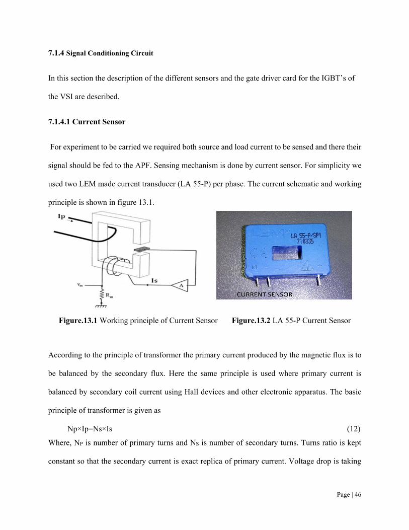
7.1.4.1 Current Sensor
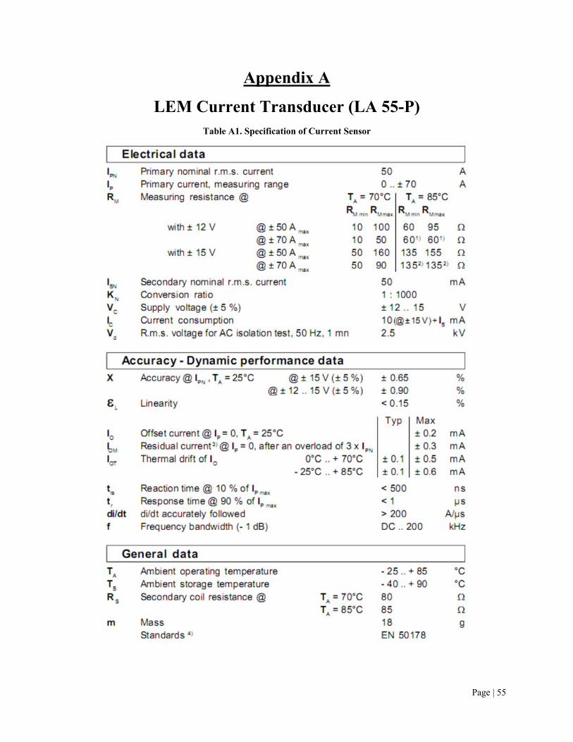
For experiment to be carried we required both source and load current to be sensed and there their
signal should be fed to the APF. Sensing mechanism is done by current sensor. For simplicity we
used two LEM made current transducer (LA 55-P) per phase. The current schematic and working
principle is shown in figure 13.1.
Figure.13.1 Working principle of Current Sensor Figure.13.2 LA 55-P Current Sensor
According to the principle of transformer the primary current produced by the magnetic flux is to
be balanced by the secondary flux. Here the same principle is used where primary current is
balanced by secondary coil current using Hall devices and other electronic apparatus. The basic
principle of transformer is given as
Np×Ip=Ns×Is (12)
Where, NP is number of primary turns and NS is number of secondary turns. Turns ratio is kept
constant so that the secondary current is exact replica of primary current. Voltage drop is taking

Page | 47
place due to the resistance RM (100 Ω) on the secondary side, and this voltage drop due to
secondary current act as an output signal of the current sensor. But we have to limit the output
voltage to the data acquisition card within analog limit of ±10 volt, for that a non-inverting
configuration opamp is used with two resistance RF and RI to select the proper gain of operation.
Both the opamp and current sensor require ± 15 volt supply for operation.
Two current sensor cards per phase are required for sensing
1. Source current
2. Load current
Current sensor card for measuring source current
Source current is limited to 10 A r.m.s, and thus current sensor card is designed keeping in mind
the maximum limit of current output of the source current. It is calibrated such that for 1 A of
source current output signal will be 2V. Using MATLAB or some other method curve fitting
formula for current sensor card measuring the source current can be computed as
2.189 0.1207 …………. (13)
Current sensor card for measuring load current
Similarly load current is limited to a maximum value of 40 A r.m.s and for measuring this the
current sensor is calibrated as 2 A of load current gives 1 V of output voltage. Using MATLAB or
some other method curve fitting formula for current sensor card measuring the source current can
be computed as
2.192 0.1081 …………. (14)
Page | 48
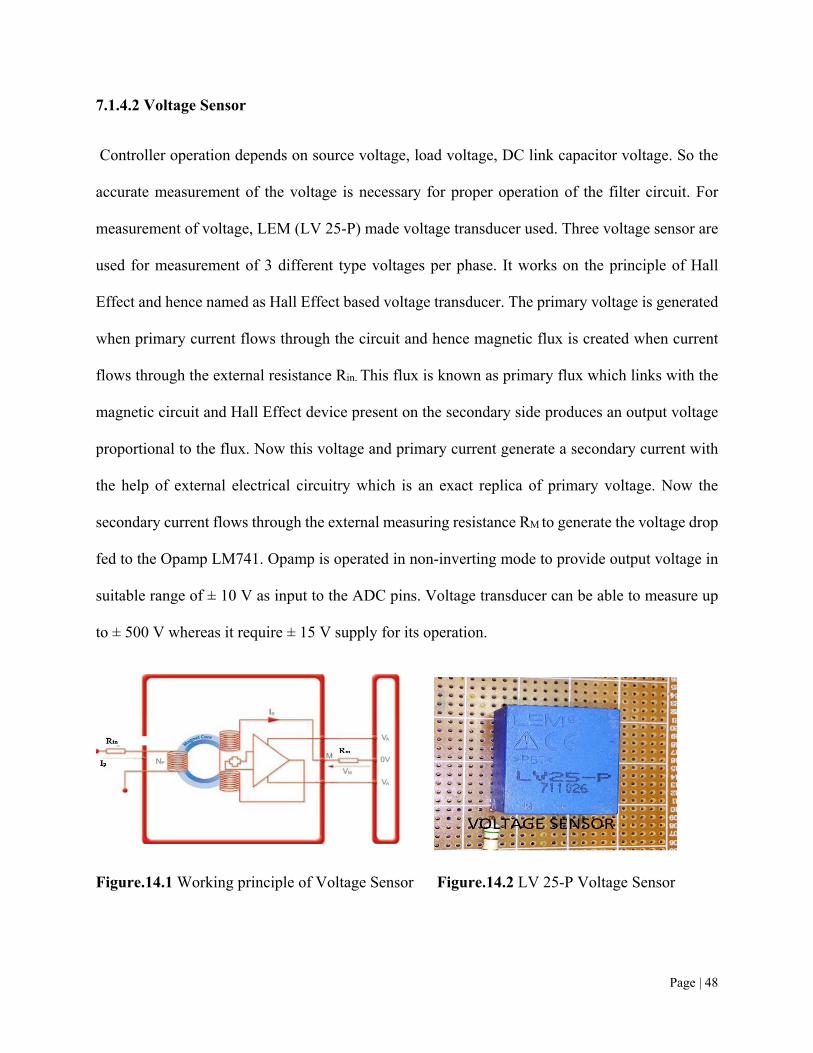
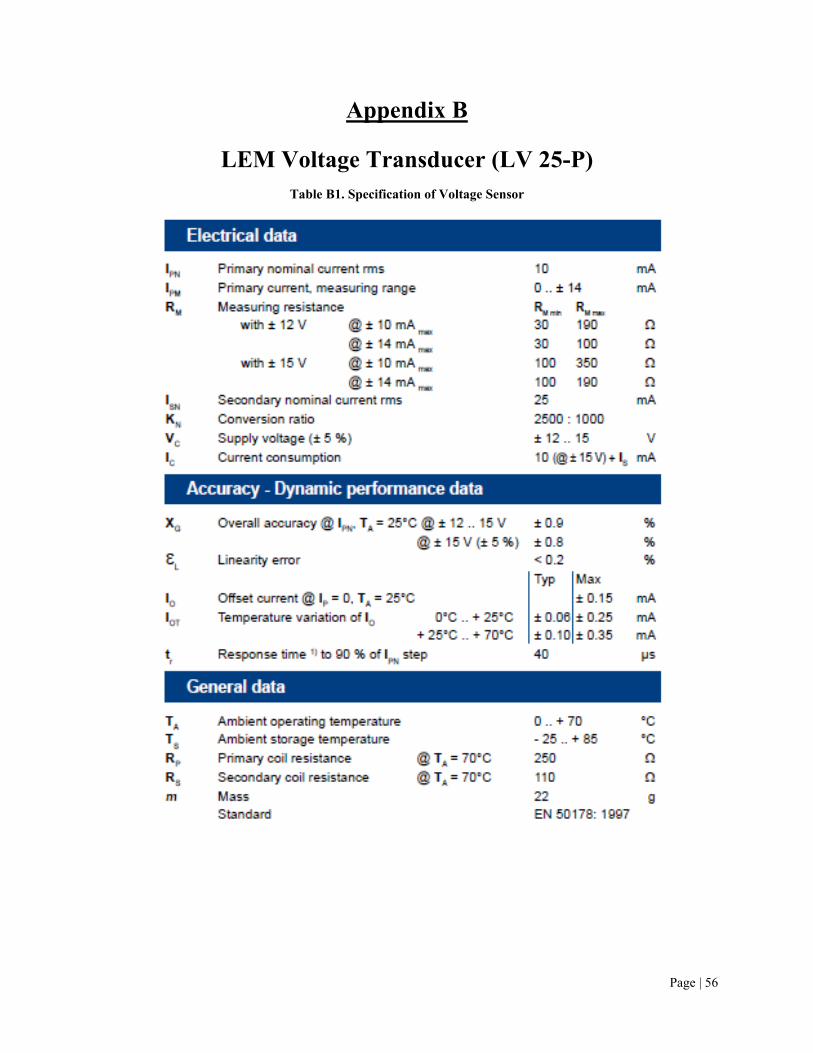
7.1.4.2 Voltage Sensor
Controller operation depends on source voltage, load voltage, DC link capacitor voltage. So the
accurate measurement of the voltage is necessary for proper operation of the filter circuit. For
measurement of voltage, LEM (LV 25-P) made voltage transducer used. Three voltage sensor are
used for measurement of 3 different type voltages per phase. It works on the principle of Hall
Effect and hence named as Hall Effect based voltage transducer. The primary voltage is generated
when primary current flows through the circuit and hence magnetic flux is created when current
flows through the external resistance Rin. This flux is known as primary flux which links with the
magnetic circuit and Hall Effect device present on the secondary side produces an output voltage
proportional to the flux. Now this voltage and primary current generate a secondary current with
the help of external electrical circuitry which is an exact replica of primary voltage. Now the
secondary current flows through the external measuring resistance RM to generate the voltage drop
fed to the Opamp LM741. Opamp is operated in non-inverting mode to provide output voltage in
suitable range of ± 10 V as input to the ADC pins. Voltage transducer can be able to measure up
to ± 500 V whereas it require ± 15 V supply for its operation.
Figure.14.1 Working principle of Voltage Sensor Figure.14.2 LV 25-P Voltage Sensor
Page | 49
Three voltage sensor cards are used for measurement of:
1. Source voltage
2. Load voltage
3. DC link capacitor voltage
All the voltage sensors are designed to measure a maximum voltage of 500V (470 V r.m.s). The
input resistance used for measurement of primary voltage of the transducer considering maximum
accuracy at optimal primary current of 10mA, was 50KΩ/5W. At the output side for measurement
of voltage a resistance of 65KΩ/5W was placed. The sensor is calibrated in such a manner that 10
V change in input voltage results in 1V change of output voltage. . Using MATLAB or some other
method curve fitting formula for Voltage sensor card are computed as:
For source voltage sensor, 0.0923 0.2380 …………...... (14)
For load voltage sensor, 0.0904 0.2541 ……………….. (15)
For DC link voltage sensor, 0.0941 _ 0.3541 …………… (16)
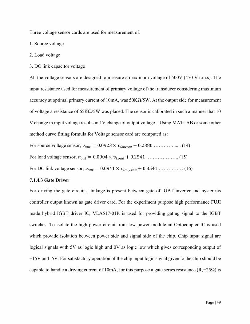
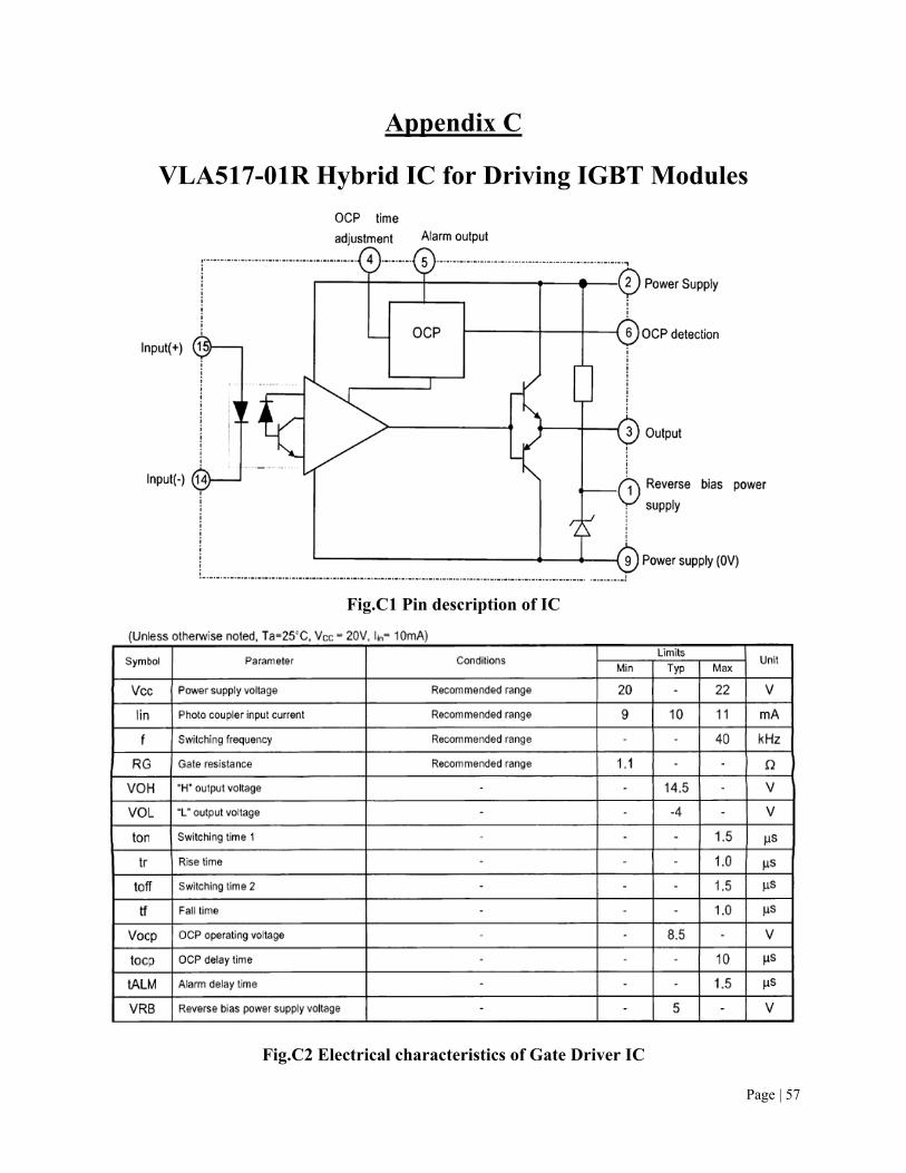
7.1.4.3 Gate Driver
For driving the gate circuit a linkage is present between gate of IGBT inverter and hysteresis
controller output known as gate driver card. For the experiment purpose high performance FUJI
made hybrid IGBT driver IC, VLA517-01R is used for providing gating signal to the IGBT
switches. To isolate the high power circuit from low power module an Optocoupler IC is used
which provide isolation between power side and signal side of the chip. Chip input signal are
logical signals with 5V as logic high and 0V as logic low which gives corresponding output of
+15V and -5V. For satisfactory operation of the chip input logic signal given to the chip should be
capable to handle a driving current of 10mA, for this purpose a gate series resistance (Rg=25Ω) is
Page | 50
used across gate emitter terminals of the corresponding IGBT. The circuit schematic diagram for
the IGBT driver is shown in Fig.15.1.
.
Figure.15.1 Working principle of gate driver circuit Figure.15.2 Gate Driver Circuit
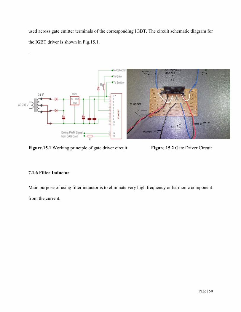
7.1.6 Filter Inductor
Main purpose of using filter inductor is to eliminate very high frequency or harmonic component
from the current.
Page | 51
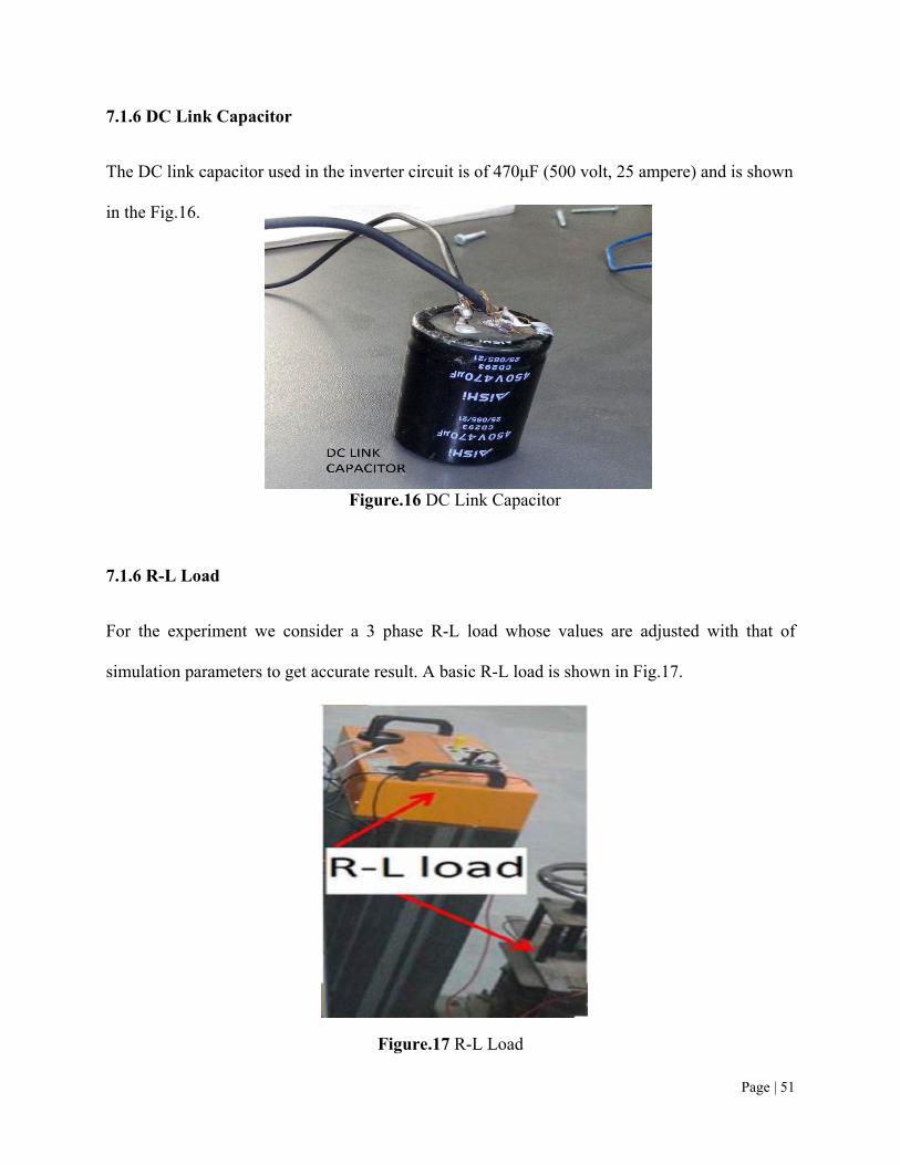
7.1.6 DC Link Capacitor
The DC link capacitor used in the inverter circuit is of 470μF (500 volt, 25 ampere) and is shown
in the Fig.16.
Figure.16 DC Link Capacitor
7.1.6 R-L Load
For the experiment we consider a 3 phase R-L load whose values are adjusted with that of
simulation parameters to get accurate result. A basic R-L load is shown in Fig.17.
Figure.17 R-L Load

Page | 52
CHAPTER-8
CONCLUSION
Page | 53
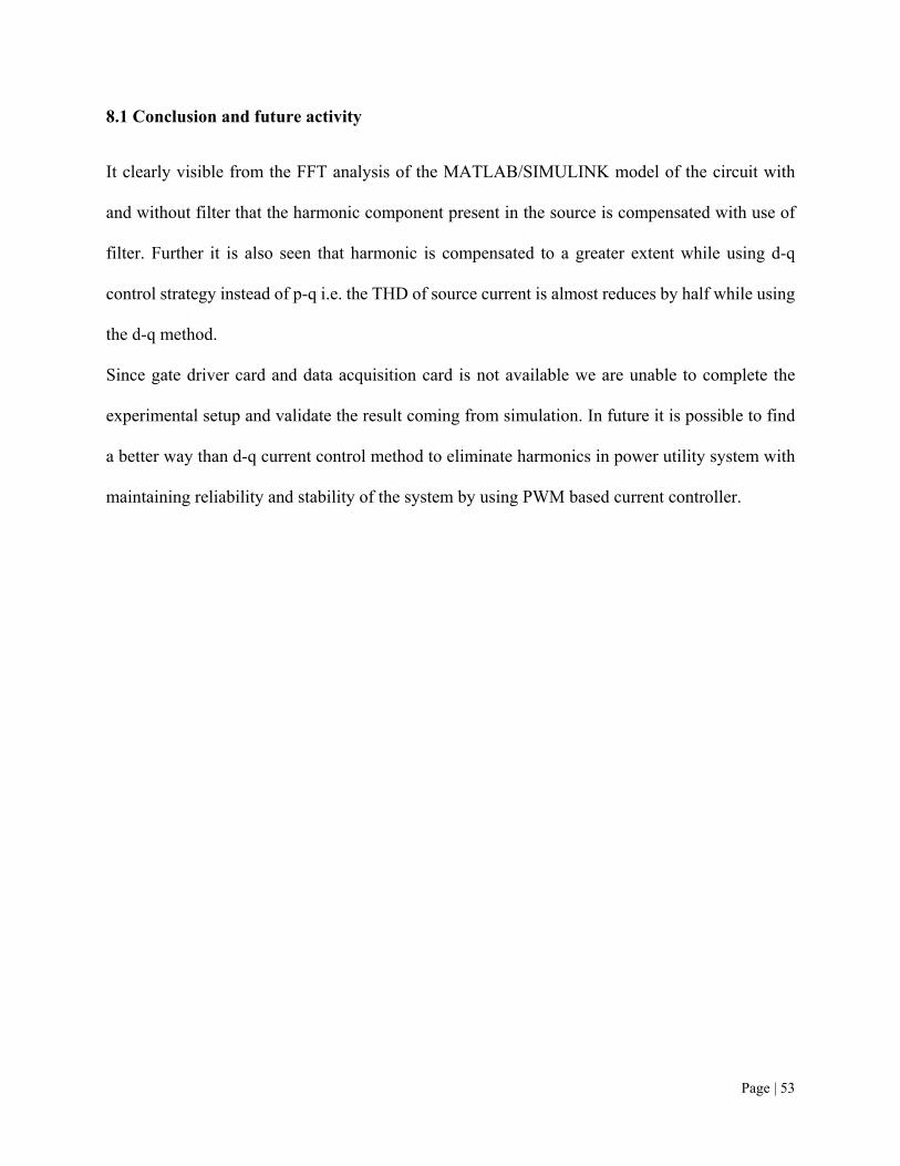
8.1 Conclusion and future activity
It clearly visible from the FFT analysis of the MATLAB/SIMULINK model of the circuit with
and without filter that the harmonic component present in the source is compensated with use of
filter. Further it is also seen that harmonic is compensated to a greater extent while using d-q
control strategy instead of p-q i.e. the THD of source current is almost reduces by half while using
the d-q method.
Since gate driver card and data acquisition card is not available we are unable to complete the
experimental setup and validate the result coming from simulation. In future it is possible to find
a better way than d-q current control method to eliminate harmonics in power utility system with
maintaining reliability and stability of the system by using PWM based current controller.
Page | 54
REFERENCES
[1] Grady, W. Mack, and Surya Santoso. "Understanding power system harmonics." IEEE Power Engineering
Review 21.11 (2001): 8-11.
[2] Morán, Luis A., et al. "Using active power filters to improve power quality." 5th Brazilian Power Electronics
Conference. 1999.
[3] Jou, H-L. "Performance comparison of the three-phase active-power-filter algorithms." IEE Proceedings-
generation, Transmission and Distribution 142.6 (1995): 646-652.
[4] Chin Lin Chen; Chen E. Lin; Huang, C.L.; , "An active filter for unbalanced three-phase system using
synchronous detection method," Power Electronics Specialists Conference, PESC '94 Record., 25th Annual
IEEE , vol., no., pp.1451-1455 vol.2, 20-25 Jun 1994
[5] B Singh, Ambrish Chandra, Kamal Al-Haddad, Bhim. "Computer-aided modeling and simulation of active power
filters." Electric Machines &Power Systems27.11 (1999): 1227-1241
[6] Akagi. H, 1996. “New Trends in Active Filters for Power Conditioning”, IEEE Transaction on Industrial
Applications, vol. 32, No.6, Dec., pp 1312-1322
[7] Akagi. H, 2006. “Modern active filter and traditional passive filters”, Bulletin of the polish academy of sciences
technical sciences vol.54.No.3.
[8] M. Suresh , S.S.Patnaik, Y. Suresh, Prof. A.K. Panda, “Comparison of Two Compensation Control Strategies for
Shunt Active Power Filter in Three-Phase Four-Wire System”, Innovative Smart Grid Technology, IEEE PES,
17-19 Jan. 2011, pp. 1 - 6.
Page | 55
Appendix A
LEM Current Transducer (LA 55-P) Table A1. Specification of Current Sensor
Page | 56
Appendix B
LEM Voltage Transducer (LV 25-P) Table B1. Specification of Voltage Sensor
Page | 57
Appendix C
VLA517-01R Hybrid IC for Driving IGBT Modules
Fig.C1 Pin description of IC
Fig.C2 Electrical characteristics of Gate Driver IC
Page | 58
Appendix D
1) abc to d-q transformation via α-β transformation
2
3
11
2
1
2
0√3
2
√3
2
cos ∅ sin∅sin∅ cos ∅
2
3
cos ∅ cos ∅ cos ∅sin∅ sin ∅ sin ∅
2) d-q to abc transformation via α-β transformation
=cos ∅ sin∅sin∅ cos ∅
1 01
2
√3
21
2
√3
2
cos ∅ sin ∅cos sincos sin
2
3
∅ Angle between d-q and αβ reference frames