power mosfet technology gate current needs in a ... 2012 doc id 023526 rev 1 1/20 an4150 application...
TRANSCRIPT

October 2012 Doc ID 023526 Rev 1 1/20
AN4150Application note
Power MOSFET technology gate current needs in a synchronousbuck converter
IntroductionHigh frequency converters and applications require the best driver-MOSFET trade-off in terms of dynamic parameters to optimize the turn-on and turn-off transients. Power MOSFET technology also plays an important role in minimizing dynamic losses and improving system efficiency.
In this document, the full characterization of Power MOSFET gate current is realized by bench tests and OrCAD® simulation results, focusing on the impact of Power MOSFET technology on gate current behavior.
Ever increasing system switching frequency pushes designers and converter engineers to optimize semiconductor technology, improving device switching behavior and system efficiency. In fact, the higher the switching frequency, the larger the switching and dynamic losses; in these conditions, the best trade-off between the driver and Power MOSFET is mandatory to enhance the overall converter performance.
Power MOSFET gate current behavior during switching transients plays an important role in establishing a good trade-off between Power MOSFET and driver performance.
In this document, Power MOSFET gate current characterization is performed through bench tests and simulations (by Cadence® OrCAD Capture) on a single-phase synchronous buck converter, allowing a full understanding of the impact of the silicon technology on device gate current.
www.st.com
Contents AN4150
2/20 Doc ID 023526 Rev 1
Contents
1 Synchronous buck converter description . . . . . . . . . . . . . . . . . . . . . . . 4
1.1 Topology and theory of operation . . . . . . . . . . . . . . . . . . . . . . . . . . . . . . . . 4
1.2 Low-side switching transients analysis . . . . . . . . . . . . . . . . . . . . . . . . . . . . 5
2 Synchronous buck converter testing demonstration board . . . . . . . . . 8
2.1 Power MOSFET selection for comparative tests . . . . . . . . . . . . . . . . . . . . 9
3 Bench tests and simulation results overview . . . . . . . . . . . . . . . . . . . . 12
4 Conclusion . . . . . . . . . . . . . . . . . . . . . . . . . . . . . . . . . . . . . . . . . . . . . . . . 16
5 References . . . . . . . . . . . . . . . . . . . . . . . . . . . . . . . . . . . . . . . . . . . . . . . . 17
6 Revision history . . . . . . . . . . . . . . . . . . . . . . . . . . . . . . . . . . . . . . . . . . . 18

AN4150 List of figures
Doc ID 023526 Rev 1 3/20
List of figures
Figure 1. Single phase synchronous buck converter topology . . . . . . . . . . . . . . . . . . . . . . . . . . . . . . 4Figure 2. HS/LS waveforms during LS turn-off . . . . . . . . . . . . . . . . . . . . . . . . . . . . . . . . . . . . . . . . . . 5Figure 3. Shoot-through event caused by dv/dt . . . . . . . . . . . . . . . . . . . . . . . . . . . . . . . . . . . . . . . . . . 7Figure 4. HS/LS waveforms during LS turn-on . . . . . . . . . . . . . . . . . . . . . . . . . . . . . . . . . . . . . . . . . . 7Figure 5. Testing demonstration board schematic. . . . . . . . . . . . . . . . . . . . . . . . . . . . . . . . . . . . . . . . 8Figure 6. Rogowski coil package for Igate measurement . . . . . . . . . . . . . . . . . . . . . . . . . . . . . . . . . . . 9Figure 7. Device A (left) and device B (right) cross sections . . . . . . . . . . . . . . . . . . . . . . . . . . . . . . . 10Figure 8. Device A (left) and device B (right) cross sections with geometrical details . . . . . . . . . . . . 10Figure 9. Gate charge comparison . . . . . . . . . . . . . . . . . . . . . . . . . . . . . . . . . . . . . . . . . . . . . . . . . . 11Figure 10. Device A gate waveforms . . . . . . . . . . . . . . . . . . . . . . . . . . . . . . . . . . . . . . . . . . . . . . . . . . 12Figure 11. Device B gate waveforms . . . . . . . . . . . . . . . . . . . . . . . . . . . . . . . . . . . . . . . . . . . . . . . . . . 12Figure 12. Device A vs. device B (experimental results) . . . . . . . . . . . . . . . . . . . . . . . . . . . . . . . . . . . 13Figure 13. Device A gate waveforms @ LS turn-off (simulated) . . . . . . . . . . . . . . . . . . . . . . . . . . . . . 14Figure 14. Device A gate waveforms @ LS turn-on (simulated) . . . . . . . . . . . . . . . . . . . . . . . . . . . . . 14Figure 15. Device B gate waveforms @ LS turn-off (simulated) . . . . . . . . . . . . . . . . . . . . . . . . . . . . . 14Figure 16. Device B gate waveforms @ LS turn-on (simulated) . . . . . . . . . . . . . . . . . . . . . . . . . . . . . 14Figure 17. Device A vs. device B (simulation results) . . . . . . . . . . . . . . . . . . . . . . . . . . . . . . . . . . . . . 15
Synchronous buck converter description AN4150
4/20 Doc ID 023526 Rev 1
1 Synchronous buck converter description
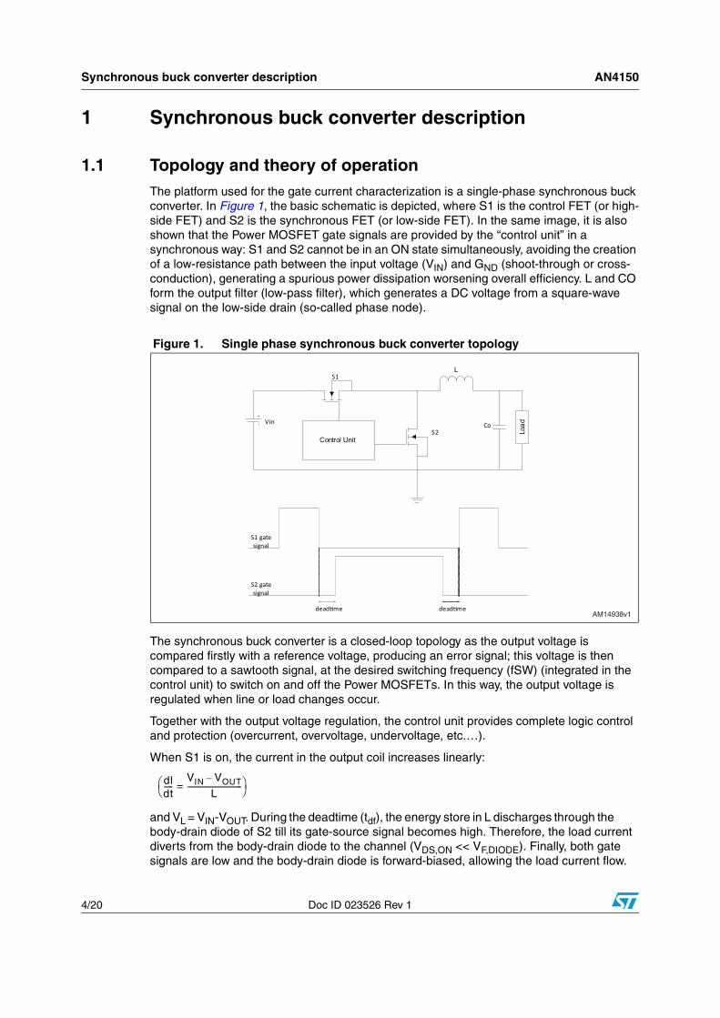
1.1 Topology and theory of operation The platform used for the gate current characterization is a single-phase synchronous buck converter. In Figure 1, the basic schematic is depicted, where S1 is the control FET (or high-side FET) and S2 is the synchronous FET (or low-side FET). In the same image, it is also shown that the Power MOSFET gate signals are provided by the “control unit” in a synchronous way: S1 and S2 cannot be in an ON state simultaneously, avoiding the creation of a low-resistance path between the input voltage (VIN) and GND (shoot-through or cross-conduction), generating a spurious power dissipation worsening overall efficiency. L and CO form the output filter (low-pass filter), which generates a DC voltage from a square-wave signal on the low-side drain (so-called phase node).
The synchronous buck converter is a closed-loop topology as the output voltage is compared firstly with a reference voltage, producing an error signal; this voltage is then compared to a sawtooth signal, at the desired switching frequency (fSW) (integrated in the control unit) to switch on and off the Power MOSFETs. In this way, the output voltage is regulated when line or load changes occur.
Together with the output voltage regulation, the control unit provides complete logic control and protection (overcurrent, overvoltage, undervoltage, etc.…).
When S1 is on, the current in the output coil increases linearly:
and VL = VIN-VOUT. During the deadtime (tdf), the energy store in L discharges through the body-drain diode of S2 till its gate-source signal becomes high. Therefore, the load current diverts from the body-drain diode to the channel (VDS,ON << VF,DIODE). Finally, both gate signals are low and the body-drain diode is forward-biased, allowing the load current flow.
Figure 1. Single phase synchronous buck converter topology
Control UnitS2
S1L
CoVin
Load
dead�me dead�me
S1 gate signal
S2 gate signal
AM14938v1
dldt-----
VIN VOUT–
L------------------------------=⎝ ⎠
⎛ ⎞
AN4150 Synchronous buck converter description
Doc ID 023526 Rev 1 5/20
During the deadtime and before the HS turn-on, the LS device must remove the charge stored in the LS body-drain diode (reverse recovery charge process) before sustaining drain-source voltage. Therefore, the body-drain characteristics, in terms of reverse recovery current and charge, seriously impact the Power MOSFET switching behavior and converter power losses, especially when the converter switching frequency rises up.
In a synchronous buck converter, the low-side drain is subjected to fast positive/negative slopes and high voltage spikes, which can exceed the low-side absolute maximum voltage, degrading the Power MOSFET reliability up unto its failure. Therefore, the right Power MOSFET choice and system configuration, device placement on the board, and the optimization of the stray inductances and parasitic, allow an important phase node spike reduction, improving the converter performance.
If tON is the HS conduction time and TS the switching period, the converter duty cycle is defined as:
Equation 1
So, the input-output relationship of a buck converter is given by:
Equation 2
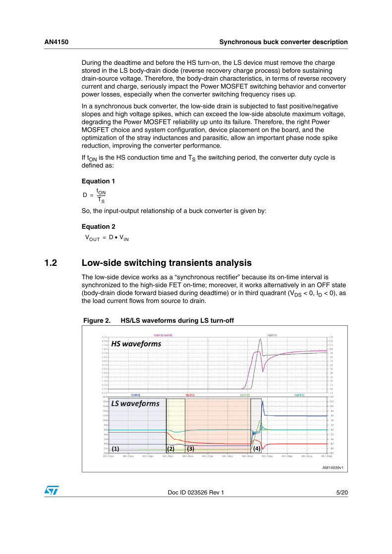
1.2 Low-side switching transients analysisThe low-side device works as a “synchronous rectifier” because its on-time interval is synchronized to the high-side FET on-time; moreover, it works alternatively in an OFF state (body-drain diode forward biased during deadtime) or in third quadrant (VDS < 0, ID < 0), as the load current flows from source to drain.
DtON
TS---------=
VOUT D VIN•=
Figure 2. HS/LS waveforms during LS turn-off
HS waveforms
LS waveforLS wavefe off r
(1) (2) (3) (4)
AM14939v1

Synchronous buck converter description AN4150
6/20 Doc ID 023526 Rev 1
In these conditions, it is interesting to analyze the switching transients.
In Figure 2, the HS and LS waveforms during LS turn-off are reported. The top half of the image shows HS VGS (purple trace) and ID (grey trace), while the bottom half shows LS VGS (red trace), VDS (blue trace), IG (light blue trace) and ID (light green trace).
The main LS turn-on steps are analyzed in detail, as follows:
1. Low-side FET is in an ON state (in this case, VGG = 5 V), with load current flowing from source to drain (green trace). At the end of (1), the driver begins to turn off the FET.
2. VGS goes down from VGG to Vth and the gate current becomes negative and starts to remove the charge stored in the device intrinsic capacitances. At the end of (2), the gate-source voltage becomes equal to the threshold voltage (VGS = Vth): so, the gate current is dropped to low values (intrinsic caps are discharged) and the load current diverts from the Power MOSFET channel to the body-drain diode.
3. During deadtime, the LS FET is in an OFF state (VGS = 0), VDS becomes negative (VDS = -VF,DIODE) and the load current flows through the body-drain diode. As a consequence, minority excess charge in both diode regions is created.
4. The LS current decreases linearly, while the HS current increases linearly in direct proportion to the fall of the LS FET current. To completely turn off the LS device, the excess stored charge in its body diode must be removed: so, the reverse recovery process generates an extra-current (IRR), which adds to the HS current. The maximum HS current peak is, therefore, given by: ID,HS = ILOAD + IRRThe spurious bouncing on the LS gate signal is caused by the voltage drop across package parasitic inductances (especially, source inductance), related to negative dl/dt (the current is falling to zero). Obviously, the bigger the parasitic inductance (package, wire bonding and layout) the higher the bouncing amplitude. At the same time, the low-side VDS is fixed by the parasitic inductance and dlD,LS/dt.
During device turn-off, the gate current is negative, because of the Power MOSFET intrinsic capacitances discharge process. The current is sunk by the driver, with a speed linked to the gate voltage level and overall gate resistance (RG,TOT = RG,INT + RDR,SINK).
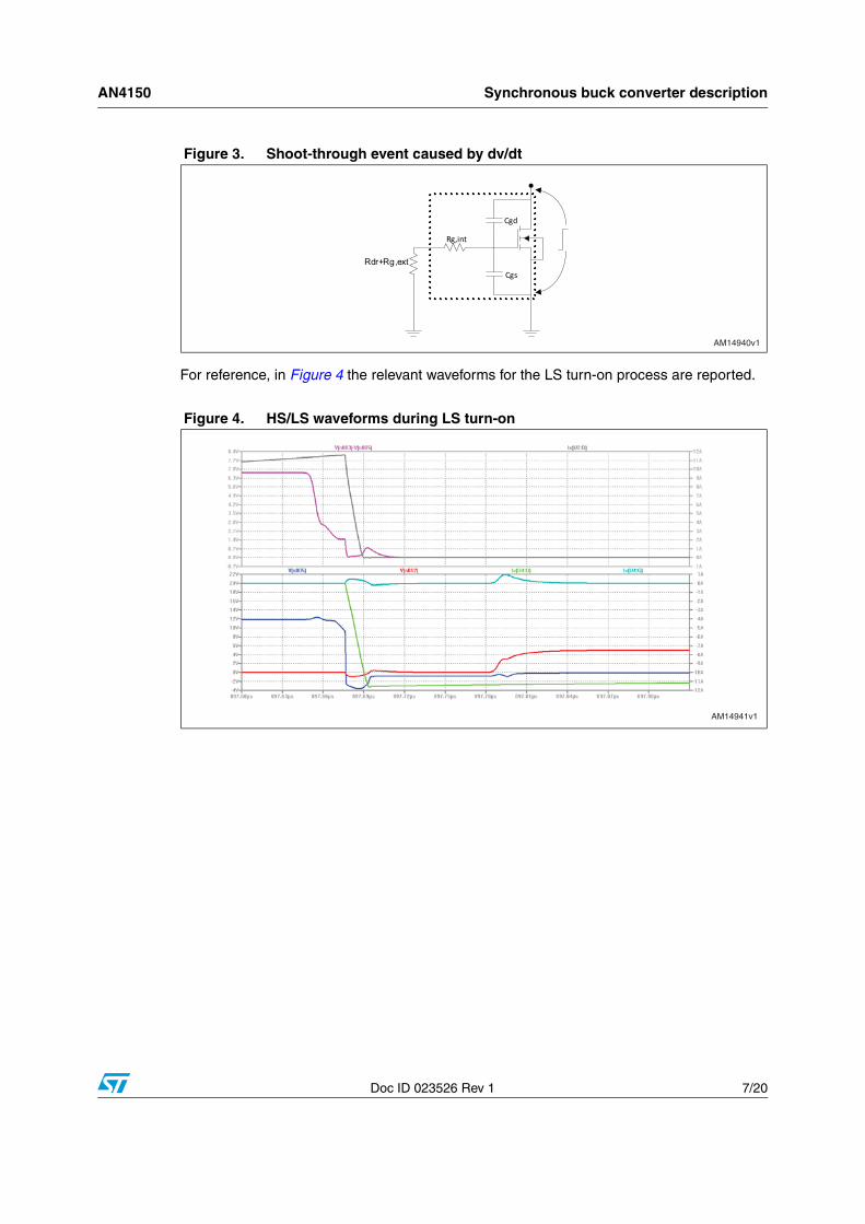
It is important to underline that, at LS turn-off, the driver, external and intrinsic FET gate resistance should be as low as possible in order to minimize the device shoot-through risks, caused by high dv/dt across drain-source, coupled to the gate signals through Miller capacitance in Figure 3.
AN4150 Synchronous buck converter description
Doc ID 023526 Rev 1 7/20
For reference, in Figure 4 the relevant waveforms for the LS turn-on process are reported.
Figure 3. Shoot-through event caused by dv/dt
Figure 4. HS/LS waveforms during LS turn-on
Cgd
Cgs
Rg,int
Rdr+Rg,ext
AM14940v1
AM14941v1

Synchronous buck converter testing demonstration board AN4150
8/20 Doc ID 023526 Rev 1
2 Synchronous buck converter testing demonstration board
The test vehicle is a synchronous buck converter, which lowers the input voltage (12 V) in 1.25 V as output; the converter switching frequency is 300 kHz, fixed by an internal oscillator, while the maximum output current is 20 A.
The converter has a single device both for high-side and low-side positions. The Power MOSFET gate drive voltage is 12 V for both devices; HS and LS external gate resistances are 2.2 Ω .
The Power MOSFETs are driven by a single-phase PWM controller with integrated driver (IHS,SRC = 2 A, RHS,SINK = 2 Ω, ILS,SRC = 3 A, RLS,SINK = 1 Ω). The controller shows very low LS sink resistance value in order to prevent any spurious gate-source bouncing and cross-conduction phenomenon during device turn-off.
The main advantage of this analysis is the availability of both the physical board and the full Cadence OrCAD Capture model of the converter (including driver and Power MOSFETs). Based on the same schematic, with identical passive and semiconductor devices, it is possible to use the converter Cadence OrCAD Capture model for testing various operating conditions, validating and explaining the experimental results. Moreover, the simulation data are very helpful to evaluate the Power MOSFET currents (especially drain current), as in the real board they cannot be measured easily by standard current probes, due to SMD packages and high switching frequency.
Figure 5. Testing demonstration board schematic
VCC
VCC BOOT
CDEC
PGOOD
RBSTDBST
CBST
UGATERG,HS
PHASERPH
VIN
CBCHF
RG,LSLGATE
ROC
RSNUB
CSNUB COUT
HS
LS
L
GNDVSEN
LOAD
RFBROS
COMP
CP
CF
RF
FB
RFBROS
RGD
VOUT
CTR+
DRV
AM14942v1

AN4150 Synchronous buck converter testing demonstration board
Doc ID 023526 Rev 1 9/20
To overcome these difficulties, in the real board, the Power MOSFET gate current measurement is made by using a “Rogowski coil” current probe (CWT ultra mini), properly connected to the Power MOSFET gate pin. The features of this device are interesting, because it is flexible and open-ended and can be wrapped around a conductor without disturbing it. Moreover, it is able to respond correctly to fast-changing currents and it is highly linear even at very high current levels.
In Figure 6, the Rogowski coil probe end placing on a Power MOSFET DPAK gate pin is shown.
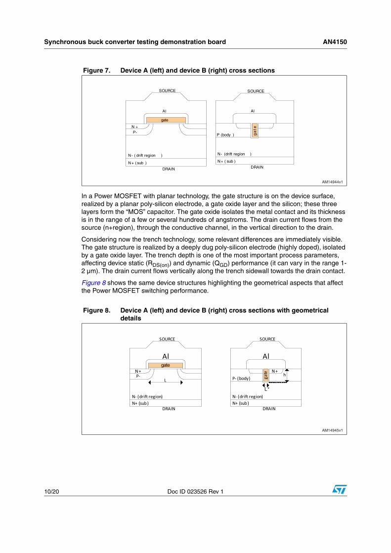
2.1 Power MOSFET selection for comparative testsThe aim of this document is to evaluate and explain the MOSFET technology gate current relationship; the analysis starts by choosing two different low-side devices, with the same die size, to be tested on the board:
a) Device A - “planar” technology
b) Device B - “trench” technology
All the devices are 30 V logic level FETs (1 V < Vth < 2.5 V). In the following table, the main Power MOSFET dynamic parameters (intrinsic capacitances and resistances) are reported:
Figure 7 gives the cross sections of the two above mentioned devices.
Figure 6. Rogowski coil package for Igate measurement
AM14943v1
Table 1. Power MOSFET electrical parameters
DeviceQG @ 4.5 V
(nC)QGS (nC)
QGD (nC)
Ciss @ 25 V Crss @ 25 V Coss @ 25 VRG (Ω)
A 14 6.8 4.7 1850 58 380 1.2
B 20 8.2 7.5 2200 280 400 1.1
Synchronous buck converter testing demonstration board AN4150
10/20 Doc ID 023526 Rev 1
In a Power MOSFET with planar technology, the gate structure is on the device surface, realized by a planar poly-silicon electrode, a gate oxide layer and the silicon; these three layers form the “MOS” capacitor. The gate oxide isolates the metal contact and its thickness is in the range of a few or several hundreds of angstroms. The drain current flows from the source (n+region), through the conductive channel, in the vertical direction to the drain.
Considering now the trench technology, some relevant differences are immediately visible. The gate structure is realized by a deeply dug poly-silicon electrode (highly doped), isolated by a gate oxide layer. The trench depth is one of the most important process parameters, affecting device static (RDS(on)) and dynamic (QGD) performance (it can vary in the range 1-2 µm). The drain current flows vertically along the trench sidewall towards the drain contact.
Figure 8 shows the same device structures highlighting the geometrical aspects that affect the Power MOSFET switching performance.
Figure 7. Device A (left) and device B (right) cross sections
Figure 8. Device A (left) and device B (right) cross sections with geometrical details
gate
Al
SOURCE
N +P-
N - ( drift region )
N + ( sub )
DRAIN
Al
SOURCE
N- (drift region )
N+ ( sub )
DRAIN
ga
te
P (body )
AM14944v1
gateAl
SOURCE
N+P-
N- (dri� region)N+ (sub)
DRAIN
L
Al
SOURCE
N- (dri� region)N+ (sub)
DRAIN
gate N+
h
L*
P- (body)
AM14945v1

AN4150 Synchronous buck converter testing demonstration board
Doc ID 023526 Rev 1 11/20
For a planar structure, L is the gate electrode width while the pitch is the cell-to-cell distance. In a trench device, L* is the trench width and h is the trench depth. Qg/A (gate charge per area) links the Power MOSFET dynamic performance to the device geometry, providing a good tool for a technology comparison:
Equation 3
Equation 4
Equation 3 is valid for a planar device, while 4 is valid for trench. For modern silicon technology, the following considerations are valid:
Equation 5
L*<< 2 h
Equation 6
L < 2 h
So, merging Equation 3, 4, 5 and 6 and considering that (pitch)A > (pitch)B:
Equation 7
Equation 8
In other words, the intrinsic capacitive contribution of planar technology is lower than that of trench. This is of basic importance when the system/application requires switching performance improvement.
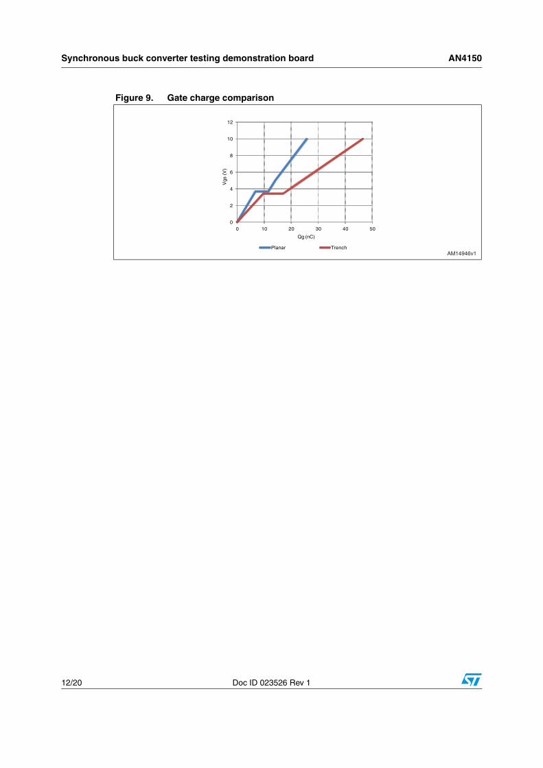
The specific capacitance difference between devices A and B shown in Figure 8 is reflected into dissimilar gate charge curves: all the components of the gate charge are much larger for dev.B (red curve).
Qg
A------- ∝ L
pitch( )A----------------------
Qg
A------- ∝ L 2h+
pitch( )A----------------------*
Qg
A-------⎝ ⎠
⎛ ⎞planar
Qg
A-------⎝ ⎠
⎛ ⎞trench
<
Cxx
A---------⎝ ⎠
⎛ ⎞planar
Cxx
A---------⎝ ⎠
⎛ ⎞trench
<
Synchronous buck converter testing demonstration board AN4150
12/20 Doc ID 023526 Rev 1
Figure 9. Gate charge comparison
0
2
4
6
8
10
12
0 10 20 30 40 50V
gs (
V)
Qg (nC)
Planar TrenchAM14946v1
AN4150 Bench tests and simulation results overview
Doc ID 023526 Rev 1 13/20
3 Bench tests and simulation results overview
By an external DC electronic load, the converter output current is fixed at IOUT = 15 A. Low-side turn-on and turn-off transients are captured. For a complete comparison in terms of gate current performance, the following parameters are measured for both devices:
– Igate,max: maximum peak during turn-on;
– Igate,min: minimum value during turn-off;
– Δt(I>0): time interval duration with Igate > 0;
– Δt(I<0): time interval duration with Igate < 0;
– Igate,avg(ON): average gate current during turn-on;
– Igate,avg(OFF): average gate current during turn-off;
– Imaint: gate current value when the device is fully ON;
– tf: low-side VGS fall time, measured from 90% to 10% of VGS;
– tr: low-side VGS rise time, measured from 10% to 90% of VGS.
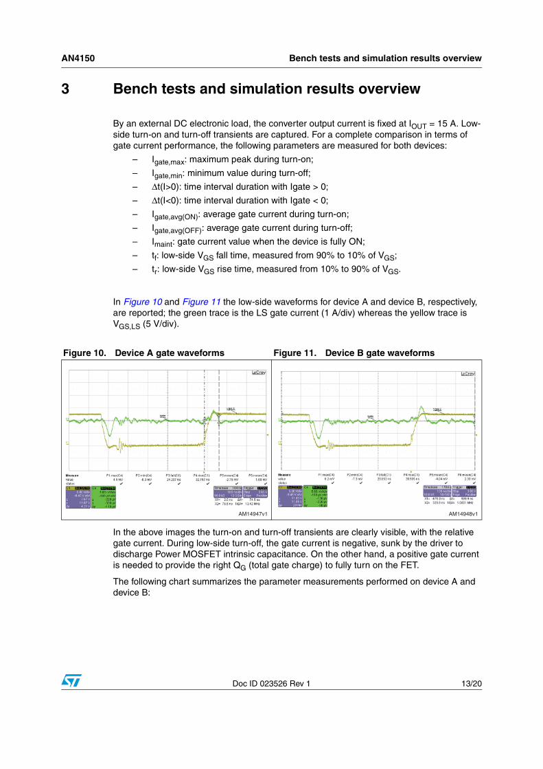
In Figure 10 and Figure 11 the low-side waveforms for device A and device B, respectively, are reported; the green trace is the LS gate current (1 A/div) whereas the yellow trace is VGS,LS (5 V/div).
In the above images the turn-on and turn-off transients are clearly visible, with the relative gate current. During low-side turn-off, the gate current is negative, sunk by the driver to discharge Power MOSFET intrinsic capacitance. On the other hand, a positive gate current is needed to provide the right QG (total gate charge) to fully turn on the FET.
The following chart summarizes the parameter measurements performed on device A and device B:
Figure 10. Device A gate waveforms Figure 11. Device B gate waveforms
AM14947v1 AM14948v1
Bench tests and simulation results overview AN4150
14/20 Doc ID 023526 Rev 1
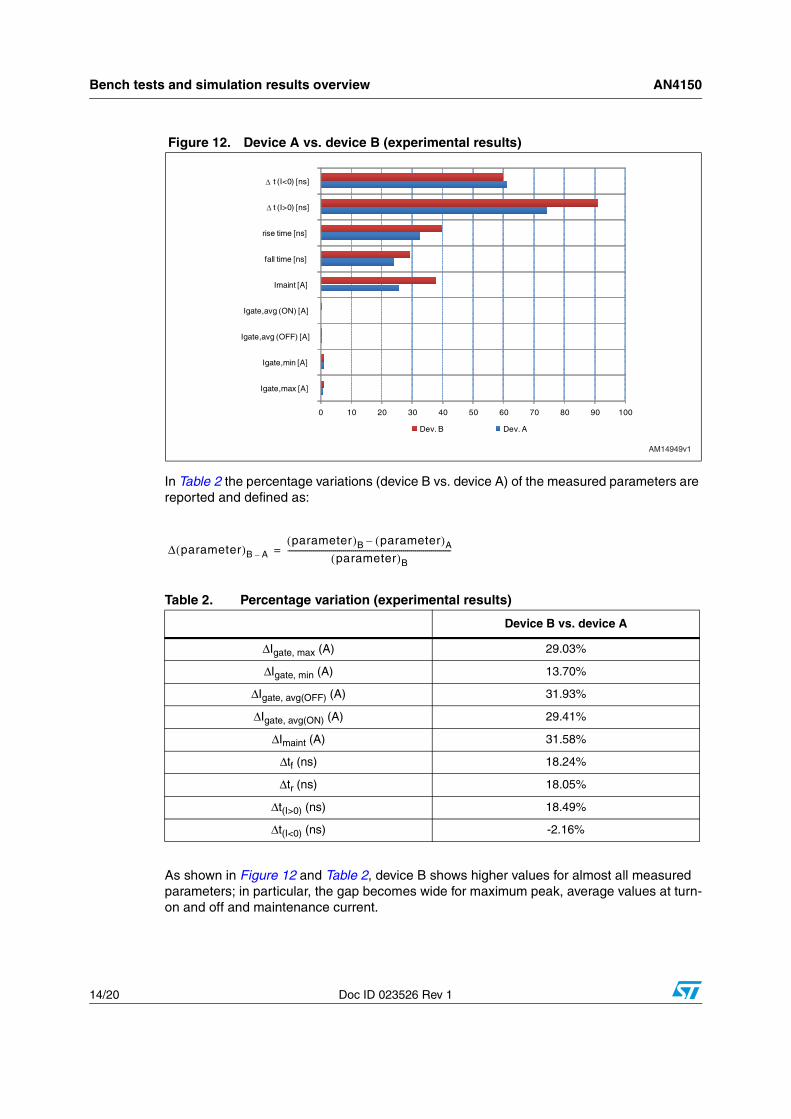
In Table 2 the percentage variations (device B vs. device A) of the measured parameters are reported and defined as:
As shown in Figure 12 and Table 2, device B shows higher values for almost all measured parameters; in particular, the gap becomes wide for maximum peak, average values at turn-on and off and maintenance current.
Figure 12. Device A vs. device B (experimental results)
Table 2. Percentage variation (experimental results)
Device B vs. device A
ΔIgate, max (A) 29.03%
ΔIgate, min (A) 13.70%
ΔIgate, avg(OFF) (A) 31.93%
ΔIgate, avg(ON) (A) 29.41%
ΔImaint (A) 31.58%
Δtf (ns) 18.24%
Δtr (ns) 18.05%
Δt(I>0) (ns) 18.49%
Δt(I<0) (ns) -2.16%
0 10 20 30 40 50 60 70 80 90 100
Igate,max [A]
Igate,min [A]
Igate,avg (OFF) [A]
Igate,avg (ON) [A]
Imaint [A]
fall time [ns]
rise time [ns]
t (I>0) [ns]
t (I<0) [ns]
Dev. B Dev. A
Δ
Δ
AM14949v1
Δ parameter( )B A–
parameter( )B parameter( )A–
parameter( )B----------------------------------------------------------------------------------=
AN4150 Bench tests and simulation results overview
Doc ID 023526 Rev 1 15/20
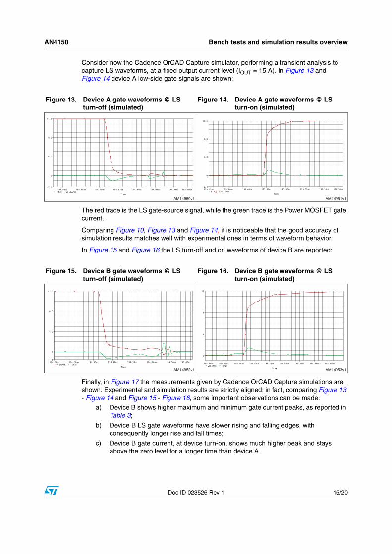
Consider now the Cadence OrCAD Capture simulator, performing a transient analysis to capture LS waveforms, at a fixed output current level (IOUT = 15 A). In Figure 13 and Figure 14 device A low-side gate signals are shown:
The red trace is the LS gate-source signal, while the green trace is the Power MOSFET gate current.
Comparing Figure 10, Figure 13 and Figure 14, it is noticeable that the good accuracy of simulation results matches well with experimental ones in terms of waveform behavior.
In Figure 15 and Figure 16 the LS turn-off and on waveforms of device B are reported:
Finally, in Figure 17 the measurements given by Cadence OrCAD Capture simulations are shown. Experimental and simulation results are strictly aligned; in fact, comparing Figure 13 - Figure 14 and Figure 15 - Figure 16, some important observations can be made:
a) Device B shows higher maximum and minimum gate current peaks, as reported in Table 3;
b) Device B LS gate waveforms have slower rising and falling edges, with consequently longer rise and fall times;
c) Device B gate current, at device turn-on, shows much higher peak and stays above the zero level for a longer time than device A.
Figure 13. Device A gate waveforms @ LS turn-off (simulated)
Figure 14. Device A gate waveforms @ LS turn-on (simulated)
Ti me
194. 86us 194. 88us 194. 90us 194. 92us 194. 94us 194. 96us 194. 98us 195. 00usI ( R2) V( LGATE)
0
4. 0
8. 0
- 2. 4
11. 9
AM14950v1 Ti me
195. 42us 195. 44us 195. 46us 195. 48us 195. 50us 195. 52us 195. 54us 195. 56usI ( R2) V( LGATE)
0
4. 0
8. 0
- 2. 4
11. 8
I ( R2)
AM14951v1
Figure 15. Device B gate waveforms @ LS turn-off (simulated)
Figure 16. Device B gate waveforms @ LS turn-on (simulated)
Ti me
194. 86us 194. 88us 194. 90us 194. 92us 194. 94us 194. 96us 194. 98us 195. 00usV( LGATE) I ( R2)
0
4. 0
8. 0
12. 0
- 1. 6
AM14952v1 Ti me
195. 44us 195. 46us 195. 48us 195. 50us 195. 52us 195. 54us 195. 56us 195. 58us 195. 60usV( LGATE) I ( R2)
0
4
8
12
AM14953v1
Bench tests and simulation results overview AN4150
16/20 Doc ID 023526 Rev 1
Starting from the simulation results, Table 3 reports the switching parameters’ percentage variations:
Table 2 and Table 3 give very good matching between experimental and simulation results, particularly for Igate,max and Igate,min (maximum and minimum gate current) and for VGS fall time. Furthermore, the trend is confirmed also for the other switching values.
Figure 17. Device A vs. device B (simulation results)
Table 3. Percentage variation (simulation results)
Device B vs. device A
ΔIgate, max (A) 30.43%
ΔIgate, min (A) 18.75%
Δtf (ns) 15.38%
Δtr (ns) 28.57%
Δt(I>0) (ns) 57.82%
Δt(I<0) (ns) 7.10%
0 10 20 30 40 50 60 70 80 90 100
Igate,max [A]
Igate,min [A]
Igate,avg(OFF) [A]
Igate,avg(ON) [A]
Imaint [A]
� [ns]
tr [ns]
Δt(I>0) [ns]
Δt(I<0) [ns]
Dev. B Dev. AAM14954v1
AN4150 Conclusion
Doc ID 023526 Rev 1 17/20
4 Conclusion
Starting from a single-phase synchronous buck converter topology, the impact of silicon technology on low-side Power MOSFET gate current has been thoroughly analyzed, by bench tests and Cadence OrCAD Capture simulations. Trench technologies, which are preferable in high efficiency DC-DC converters due to their very competitive figure of merit (FOM = RDS(on) * QG) values, have higher specific capacitance values (Cxx/A) compared to planar ones; this affects the overall device switching performance. This also means different gate current behavior, with bigger maximum and minimum gate current peaks and longer rise/fall times.
These different device characteristics should be monitored particularly when application features (switching frequency, number of paralleled devices, etc.…) are more critical for switching behavior, making driver-MOSFET matching optimization mandatory.
Two examples can be given to enforce the previous statements. When more FETs are paralleled, to minimize the overall RDS(on) and the conduction losses, the driver must charge and discharge a bigger equivalent capacitance to switch on and off the devices. So, to minimize the gate drive losses, the driver must have special features, in terms of sink/source current and resistance, particularly when driving trench Power MOSFETs.
Similarly, in hard-switching applications, where larger losses occur during switching transients, proper driver choice is needed when higher (Cxx/A) Power MOSFETs must be turned on and off, improving gate current source and sink and reducing the switching losses.
References AN4150
18/20 Doc ID 023526 Rev 1
5 References
● Power Electronics Handbook, M. H. Rashid, 2001
● Fundamentals of Power Electronics, R. W. Erickson, 2000

AN4150 Revision history
Doc ID 023526 Rev 1 19/20
6 Revision history
Table 4. Document revision history
Date Revision Changes
12-Oct-2012 1 Initial release.
AN4150
20/20 Doc ID 023526 Rev 1
Please Read Carefully:
Information in this document is provided solely in connection with ST products. STMicroelectronics NV and its subsidiaries (“ST”) reserve theright to make changes, corrections, modifications or improvements, to this document, and the products and services described herein at anytime, without notice.
All ST products are sold pursuant to ST’s terms and conditions of sale.
Purchasers are solely responsible for the choice, selection and use of the ST products and services described herein, and ST assumes noliability whatsoever relating to the choice, selection or use of the ST products and services described herein.
No license, express or implied, by estoppel or otherwise, to any intellectual property rights is granted under this document. If any part of thisdocument refers to any third party products or services it shall not be deemed a license grant by ST for the use of such third party productsor services, or any intellectual property contained therein or considered as a warranty covering the use in any manner whatsoever of suchthird party products or services or any intellectual property contained therein.
UNLESS OTHERWISE SET FORTH IN ST’S TERMS AND CONDITIONS OF SALE ST DISCLAIMS ANY EXPRESS OR IMPLIEDWARRANTY WITH RESPECT TO THE USE AND/OR SALE OF ST PRODUCTS INCLUDING WITHOUT LIMITATION IMPLIEDWARRANTIES OF MERCHANTABILITY, FITNESS FOR A PARTICULAR PURPOSE (AND THEIR EQUIVALENTS UNDER THE LAWSOF ANY JURISDICTION), OR INFRINGEMENT OF ANY PATENT, COPYRIGHT OR OTHER INTELLECTUAL PROPERTY RIGHT.
UNLESS EXPRESSLY APPROVED IN WRITING BY TWO AUTHORIZED ST REPRESENTATIVES, ST PRODUCTS ARE NOTRECOMMENDED, AUTHORIZED OR WARRANTED FOR USE IN MILITARY, AIR CRAFT, SPACE, LIFE SAVING, OR LIFE SUSTAININGAPPLICATIONS, NOR IN PRODUCTS OR SYSTEMS WHERE FAILURE OR MALFUNCTION MAY RESULT IN PERSONAL INJURY,DEATH, OR SEVERE PROPERTY OR ENVIRONMENTAL DAMAGE. ST PRODUCTS WHICH ARE NOT SPECIFIED AS "AUTOMOTIVEGRADE" MAY ONLY BE USED IN AUTOMOTIVE APPLICATIONS AT USER’S OWN RISK.
Resale of ST products with provisions different from the statements and/or technical features set forth in this document shall immediately voidany warranty granted by ST for the ST product or service described herein and shall not create or extend in any manner whatsoever, anyliability of ST.
ST and the ST logo are trademarks or registered trademarks of ST in various countries.
Information in this document supersedes and replaces all information previously supplied.
The ST logo is a registered trademark of STMicroelectronics. All other names are the property of their respective owners.
© 2012 STMicroelectronics - All rights reserved
STMicroelectronics group of companies
Australia - Belgium - Brazil - Canada - China - Czech Republic - Finland - France - Germany - Hong Kong - India - Israel - Italy - Japan - Malaysia - Malta - Morocco - Philippines - Singapore - Spain - Sweden - Switzerland - United Kingdom - United States of America
www.st.com