plastic solder paste stencil for surface mount technology · chicago, illinois, a supplier of...
TRANSCRIPT

SOLDER PASTE STENCIL FOR SURFACE MOUNT TECHNOLOGY
Christopher K. Wong, Research Assistant! Daniel J. Waldorf, Assistant Professor
Lawrence Rinzel, Instructor
Industrial and Manufacturing Engineering Department California Polytechnic State University
San Luis Obispo, CA, 93407
Biography
Christopher Wong received his B.S. in manufacturing engineering from the California Polytechnic State University at San Luis Obispo in 1999. His coursework included manufacturing process design and development, while utilizing computer aided methods. Progressive coursework lead to emphasis in electronic manufacturing while utilizing prototyping techniques, project planning, and production methods. He has worked as a quality engineer in 1999 at LTD Ceramics in Newark, CA, a hlly integrated supplier of high purity, technical ceramic materials and machined components to the semiconductor, medical, and space industries. Currently he works as a test engineer at KLA- Tencor Corporation in San Jose, CA with the eleclron beam metrology division providing manufacturing support to their critical dimension scanning electron microscope. His interests lie in the design, development, improvement, and management of manufacturing processes within every aspect of the electronics and semiconductor industry.
Dr. Ilaniel Waldorf received his B.S. and M.S. in industrial engineering from the University of Illinois in Urbana-Champaign in 1989 and 1991, respectively. He earned his Ph.D., also from the University of Illinois, in mechanical engineering in 1996. His coursework and research concentrated on manufacturing processes and mechanical models for machining. From 1996 to 1998, he worked as a quality engineer at ATF in
Chicago, Illinois, a supplier of formed and machined components to the automotive industry. Since 1998, Dr. Waldorf has been an Assistant Professor in the Industrial, and Manufacturing Engineering Department at California Polytechnic State University in San Luis Obispo. His teaching and research interests involve design, modeling, and control of manufacturing processes and systems.
Larry Rimel received his, M.S. in Industrial Engineering at California Polytechnic State University in San Luis Obispo and currently teaches electronics nnanufacturing and engineering analysis. His research and coursework concentrated on electronics manufacturing, fuzzy logic and engineering within medical settings. Hc: worked at EMPF in Indianapolis in 1995 building a fuzzy logic database for estimating first article machine settings in an electronics SMT assembly line and at TRW during 1996 to 1997 statistically evaluating circuit board!s for space-fight applications. His interests include electronic design and manufacture, engineering medical setting systems and the use of fuzzy logic within medical databases for identification of inappropriate utilization.
Abstract:
Solder paste masks or stenc.ils are an integral part of the manufacturing process for surface mount circuit boards. This study will examine the feasibility of developing a process for rapidly
' Currently at IUA-Tencor Corporation, San Jose, CA 0-7803-6482-1 /OO/$lO.OO 02000 IEEE
2000 IEEWCPMT Int'l Electronics Manufactluring Technology Symposium
294
Authorized licensed use limited to: Cal Poly State University. Downloaded on May 8, 2009 at 14:41 from IEEE Xplore. Restrictions apply.

a solder paste stencil using a thermoplastic material. CNC laser cutting of the stencil geometry is replacing traditional use of chemical etching on metal sheets to produce the stencils. Laser cutting has been used to improve the speed, accuracy, and cost of the process. This research will attempt to continue to simplify and reduce costs in the stencil making process by proposing as the stencil material a common thermoplastic that can be cut easily and quickly using a low-power rapid-prototyping laser process. The effects of several variables on the success of the process are experimentally tested to determine a feasible solution. Various solder pastes and solder material characteristics are studied for their effect on the new material. Stencil dimensions, including thickness and aperture characteristics, are examined. Several key process factors are also varied in the tests to determine recommendations for settings such as print direction, alignment procedures, squeegee pressure and attack angle, print speed, and stencil release method. Subjective evaluation is also made of important qualities of the paste in reaction to the new material, including paste roll and consistency, paste volume, adherence, and instances of cold slumping. The resulting process will be demonstrated by producing plastic stencils on a rapid prototyping laser housed in the Cal Poly laboratories. Cost, cycle time, and performance characteristics of the plastic stencil will be estimated.
Data: Process Design Parameters
Several aspects of the plastic stencil-making process were selected for investigation. The first decision involved selecting the proper plastic material to be used. Initially a material called Lexan was selected. Lexan, which was developed by GE Plastics [16], is an amorphous thermoplastic that can be transparent or opaque, is resistant to impact, and is dimensionally stable, even at high temperatures. Since there is no record of using solder paste on plastic, the solder paste may have an adverse chemical effect on certain plastics. Therefore, other plastics such as
0-7803-6482-1/00/$10.00 02000 IEEE
polypropylene and polyethylene were also considered for their unique quality to resist many organic solvents. Lastly, acrylic was considered due to its impressive stiffness. Unfortunately, no acrylic plastic sheets less than 1.5 mm thick could be found from commercial vendors [3]. Instead, an ordinary plastic sheet of copier transparency film was chosen. According to the 3M Corporation’s Material Safety Data Sheets [ 11, transparency film is an acrylate copolymer having properties similar to acrylic though thinner in thickness.
The feasibility of using plastic stencils, given solder paste properties and characteristics, must be considered in light of creating quality print results and reliable solder joints. Hwang [20] suggests several performance parameters of solder paste, which this project will analyze, including:
1. Physical appearance. 2. Stability and shelf life 3. Viscosity 4. Cold Slump 5. Dispensability through fine needles 6. Screen or stencil printability 7. Tack time 8. Adhesion 9. Exposure life 10. Quality and consistency
Two types of solder paste samples with varying levels of each property will be used to screen print through plastic stencils. The first, ESP 566 No Clean solder paste donated by Rantec in Los Osos, California [31], has 89.5% metal content, a Type 2 powder size of 45-75 microns, and a viscosity of 750Kcps 50 under the Brookfield test. The Type 2 powder size refers to the paste being used for a pad pitch greater than .025”. The solder alloy content is a mixture of tin, lead, and silver, consisting of 62Sn/36Pb/2Ag. The paste has a tack time greater than 8 hours, meaning that the tackiness will have minimal change under varying humidity exposure for a work shift of 8 hours or more. A long tack time helps maintain consistency and reduce variations
2000 IEEWCPMT Int‘l Electronics Manufacturing Technology Symposium
295
Authorized licensed use limited to: Cal Poly State University. Downloaded on May 8, 2009 at 14:41 from IEEE Xplore. Restrictions apply.

printing as the paste is exposed to the environment. The second sample, donated by Solectron of San Jose, California, is Ultraprint 78 froxri Alpha Metals [2J. Ultraprint 78 is also a No Clean type solder paste comparable to ESP 566. The outstanding feature of the Ultraprint 78 is that it is formulated for standard and fine pitch printing through stencil apertures as small as 0.008” and pads with a pitch of 0.016”. The Ultraprint 78 also possesses a tack time of over 8 hours. It has 89.8% metal content, a viscosity of 2880 poise under the Malcolm test, and a Type 3 powder with 40-49 micron powder size. Type 3 provides that the paste is suitable for pitches over .018”’. The Ultraprint 78 alloy composition differs from the ESP 566 in that it does not have silver, and consists of a 63Sd37Pb alloy. This could be visually noted as the most significant difference between the two pastes, as indicated by the difference in coloration of the two. The Ultraiprint 78 has a consistent light gray tone to it, while the ESP 566 shows signs of silver content by having silver ’ speckles dispersed within a darker gray paste.
Because the use of plastic as a stencil material could have ramifications for the printing (solder paste: application) process, several parameters were selected for experimentation to determine appropriate levels of each. These include print direction, printing speed, printing pressure, and printing attack angle. In addition, since registration and alignment of the stencil could interact with any of these parameters, it was selected as a noise variable in the experiments.
Lastly, once the paste has been applied through a stencil, releasing that stencil from the printed PCB is the most crucial process for attaining a successfbl print. The conventional method to help release solder paste from apertures is called snapoff. Snap-off minimizes solder paste contact with the walls of the aperture by placing the stencil above the PCB a distance of 0.020” to 0.050”. A newer alternative to snap-off is a “conrrolled release” as described by Rowland [26]. This is where the speed of the stencil being pulled away can be controlled. Rowland says,
“slow release will give the solder paste time to break free from the aperture wall.” Another factor, pulling the stencil straight off versus peeling the stencil away slowly will be included in the experimentation.
Experimentation
Experimentation was designed to test the plastic material selected for the stencil, two types of solder paste, several printing process parameters including alignment of stencil to circuit board, and an appropriate stexilcil release method. Observational characteristilcs analyzed include percentage of paste adhesion, visual paste consistency, ease of solder paste roll, paste volume, and instances of cold slumping. These observations qualify the success of each of the experimental factors.
Preliminary Testing for Plastic Material Selection--Several of the plastic types were quickly dismissed as potential candidates for the stencil process. A sample of a Lexan extruded sheet was obtained from Central Coast Plastics [14] measuring 1/32” thick. The sheet was tested by conducting a simple, straight-line laser cut across it using a Helisys rapid prototyping laser originally designed to cut through layers of paper. The outcome showed that this type and thickness of plastic would be difficult to use. It took several passes of the laser to cut through the sheet. During cutting there was noticeable flaming of the sheet due l:o the inability of the laser to cut entirely through. Polypropylene and polyethylene samples fiornl American Acrylics [4 J were dismissed fiom consideration because they were found to have even lower impact strength than acrylic and would prove to be far below the requirements of this project.
Next, the acrylate copolymer copier transparencies were obtained, and three straight lines were cut in a test piece using the Helisys laser. The .0045” thick transparency plastic required only one pass to penetrate the material as opposed to the many passes required to cut the thicker Lexan. Due to CAD/CAM software
0-7803-6482-1/001$10.00 02000 IEEE 2000 IEEWCPMT Int‘l Electronics Manufacturing Technology Symposium
296
Authorized licensed use limited to: Cal Poly State University. Downloaded on May 8, 2009 at 14:41 from IEEE Xplore. Restrictions apply.

a usable CAM file of a typical stencil pattem could not be generated for the Helisys laser. Instead, two transparencies were cut into stencils with surface mount pad apertures using an X-acto blade. One transparency had two sets of surface mount aperture patterns (8 pin Small Outline Integrated Circuit, 0.050” pitch, 0.020” by 0.070”) and a second transparency had one set the same as the first plus two pad apertures for each of following dimensions: 0.100” by 0.100”, 0.060” by O.lOO”, and 0.040” by 0.040”. These dimensions allowed for acceptable aperture aspect ratios (Figure 1. width of aperture opening to stencil thickness) according to guidelines in [25].
Preliminavy Testing of Stencil Release Method-- Preliminary testing of the stencil release method used the industry standard planar lifting method where the entire stencil is lifted straight off the printed board in one movement (as used by the MPM semi-automatic stencil printer in the Cal Poly Stanford Telecom Electronic Manufacturing Laboratory). An alternative method of stencil release developed due to the flexibility in the plastic transparency is a peel away method similar to peeling away a piece of tape. This method will aid in reducing the scooping effect on the printed solder paste from the sidewalls in the apertures of the plastic stencil. Both methods were tested for use with the plastic stencil.
Main Experimental Tests--A total of 64 printing tests were performed using two levels of each as described earlier for solder paste, print direction,
0-7803-6482-1/00/$10.00 02000 IEEE
printing speed, printing pressure, printing attack angle, and stencil alignment to substrate. The first set involved placing the plastic stencil on two substrates (a bare copper board and an etched printed circuit board), and varying print pressure and speed of a polyurethane squeegee blade for each of the two solder pastes. The experimental stencils were cut with a minimum pad pitch of .050” between centers of the pads. For the ESP 566 solder, printing specifications were followed that recommended a paste ‘bead volume of 20 to 30 grams of paste per inch squeegee length, a 3/8” to %” diameter roll of paste, and a paste temperature between 70” to 77”. The recommended squeegee blade is a stainless steel blade due to greater affinity for paste adhesion than polyurethane blades, although a polyurethane blade of durometer at least 80 is also acceptable. The print speed recommended is ?4” to 2” per second to maintain good roll of paste across the stencil. Excessive high or low print speeds may cause sliding. The amount of pressure applied to the stencil should be 1 to 1.5 pounds per inch squeegee length. The recommended print specifications of the Ultraprint 78 paste suggest a metal squeegee but a 90 durometer polyurethane squeegee is acceptable. Pressure should be 1-2.5 pounds per inch of print pattem. The paste volume should induce a roll of 0.4” to 0.6” diameter and add paste when the roll reaches 0.2” diameter. By holding the squeegee in one hand, the squeegee speed and pressure was varied by first, using a slow gradual stroke, while applying great downward pressure with the hand; second, with the same gradual slow stroke, but applying less pressure; third, using a quicker stroke of the squeegee, and a heavy downward pressure; and fourth, using the quick stroke with a light pressure.
The remaining tests were performed by repeating the above experiments for two levels of squeegee attack angle, two levels of print direction, and two levels of stencil alignment. The squeegee attack angle was varied by setting up the alignment of the squeegee square with the stencil and then at forty-five degrees to the stencil. This
2000 IEEUCPMT Int’l Electronics Manufacturing Technology Symposium
297
Authorized licensed use limited to: Cal Poly State University. Downloaded on May 8, 2009 at 14:41 from IEEE Xplore. Restrictions apply.

was setup to determine if the angle of squeegee printing would present better results than the conventional squared printing. Altering the print direction of the squeegee was conducted by printing with the stencil placed in one direction and by rotating the stencil and circuit board 90 degrees. The purpose of alternating the directions is to determine if the width of a pad has any effect on print quality. The registration and alignment of the stencil were varied by offsetting the apertures of the stencil from the pads of the circuit board in each axial direction of the pads. The purpose of varying this factor was to determine if misalignment would have any effect on the tack and adhesion properties of solder paste to the non-copper portions of the fiberglass substrate. The first level entailed 50% misalignment in the horizontal or x-axis and the seco:nd with 50% misalignment in the vertical or y-=:is of the pads.
In order to validate the hand cut transparencies to be representative of a laser cut stencil, a final test was conducted with the two solder pastes over a transparency with the three laser cut lines from the llelisys machine. This test would analyze what effects a laser cut stencil might have on print quality.
The major observational factors analyzed through expe:rimentation are: paste consistency, paste roll, the amount of solder paste adhering to the subsirate, the printed paste volume and height, and if any cold slumping or bridging of pads occurred. These were used to determine the best levels for each of the six factors. The amount of paste adhesion is represented by the percentage of paste passing through the stencil and adhering to the substrate. Measurement of the paste volume was by visual inspection to see if there was adequate paste height for chip placement. Cold slumping was also indicated by visual inspection for inadequate print quality and possible pad bridging.
Results and Discussion
Preliminary Test Results--The preliminary tests showed that the acrylate copolymer transparency could be cut with the Helisys rapid prototyping laser and that the peel aw,ay method of stencil release is preferable. The Lexan plastic sheet, despite having qualities and characteristics similar to stainless steel, proved to be difficult to cut with the Helisys laser and thus was not used as a stencil in the subsequent tests. It was also discovered that releasing thie stencil with planar lifting from the substrate must be done carefully and slowly to prevent lifting the sides of the paste that creates the scooping effect. Although this is not a defect due to the solder paste or the printing process, employing the peel away method may reduce this lifting of the paste. In the majority of tests using the slow peel away method, good pad print volume was observed compared to the snap off method. It was also observed that about 1% of solder paste remained in the aperture walls due to the roughness and irregularity of the cuts into the plastic. This, however, proved insignificant because the overall structure of volume within the printed pads was intact well enough to place an 8 pin SOIC chip onto the printed solder paste.
0-78036482-1/001$10.00 02000 IEEE 2000 IEEWCPMT Int'l Electronics Manufacturing Technology Symposium
298
Authorized licensed use limited to: Cal Poly State University. Downloaded on May 8, 2009 at 14:41 from IEEE Xplore. Restrictions apply.
Test Results and Discussion--Comparison of the ESP 566 and Ultraprint 78 solder pastes was difficult as both resulted in similar outcomes. The experiments conducted showed proper paste release in the results of all printing tests, indicating proper aperture aspect ratio. Tests with the Ultraprint 78 showed consistent results, with a smooth and creamy paste that could be seen with a nice rolling bead in front of the squeegee. This is a desirable characteristic in a solder paste and means that it is suitable for this printing application on a plastic stencil. However, though the ESP 566 did show some evidence of paste exposure indicated by low viscosity as the flux began to overcome the adhesiveness of the solder paste, the ESP 566 had a slight overall margin of better paste consistency, viscosity, print roll, tack, and print quality than the Ultraprint 78. No evidence of chemical reaction between either type of solder paste and the plastic copier transparency was apparent.
The appropriate speed and pressure from the use of the ESP 566 solder paste was determined to be the application of a slow squeegee stroke speed in combination with minimal pressure on the squeegee. When higher pressure and faster strokes were used, the solder paste spread underneath the stencil (between circuit board and stencil) and created solder bridges (also known as slumping). Combined high speed and high pressure achieved far less solder paste volume (almost 50% less) and visually not enough paste to secure a chip onto the circuit board. The slower pace and lighter pressure left a layer of paste coating the top surface of the stencil. However, this method proved to be successful because when the plastic stencil was removed, print quality and volume looked very similar to the initial print outcome with a metal stencil. (This is unconventional because with metal stencils the extra paste on top of the stencil is swept clean across and only remaining in the apertures). Since metal stencils tend to be thicker, the thin film of paste over the plastic stencil provided extra volume in the apertures.
0-7803-6482-1/00/$10.00 02000 IEEE
Outcomes using the Ultraprint 78 solder paste yielded similar results. Again, use of a slow squeegee stroke combined with light pressure while leaving a thin film of the paste over the plastic stencil resulted in good pad print definition over other levels of pressure and speed.
Changing the squeegee attack angle in all cases produced poor results in pad quality. The pad definition and paste volume for printing at 45 degrees to the stencil pad apertures were too thin to be acceptable for placing components onto the substrate. Moreover this printing technique produced smearing and bridging of the pad prints, which is highly undesirable. However, some improvement in paste roll was achieved by making a slight angle between the squeegee and stencil in the direction of travel (blade is typically perpendicular to print direction). This technique also led to better pad definitions and better print quality.
Printing in the direction of the stencil where the squeegee meets the majority of smallest aperture widths yielded best results overall when using low pressure and slow squeegee speed. However, less satisfactory results were achieved using quick stroke speeds with both high and low amounts of pressure perpendicular to the above print direction, where the squeegee meets the majority of wide widths. High speed combined with high amounts of pressure literally wiped away the solder paste. This was due in part to the aperture of the pad in this case being much wider thus allowing the blade to deform into the aperture and wiping or pulling the solder paste away. Using less pressure and a quick squeegee stroke faired worse. This was due to the speed of the blade moving by so quickly that it did not allow the paste to adhere to the board before the squeegee could shear the paste. This effect of print direction is not typically seen with metal stencils.
Alignment of the stencil apertures to the circuit board pads was tested for volume of paste adhesion. As it turned out, misalignment of the stencil to the circuit board did not affect any print
2000 IEEWCPMT Int'l Electronics Manufacturing Technology Symposium
299
Authorized licensed use limited to: Cal Poly State University. Downloaded on May 8, 2009 at 14:41 from IEEE Xplore. Restrictions apply.

~
or the adhesion of the paste to the circuit board. The four combinations of speed and pressure yielded similar trends as before in print quality and solder paste adhesion characteristics. In the 50% aperture-to-pad misalignment testing, visual inspection revealed that distinct solder volume adhered to both the substrate (FR-4) and the copper pads for all misaligned axes.
The validation test on the laser cut stencil was also observed for print quality. Initially, due to heat from the laser cutting through the transparency and melting back the walls, it was thought that the inner walls of the apertures were too jagged and rough and would lead to the lift- off of the solder paste after printing. After smearing the solder paste over the stencil with the various print methods and combinations of pressure and stroke speed introduced above, it was discovered that there were no adverse effects to print quality due to the structure of the aperture walls from the laser cutting. Using visual inspection, relatively little (less than 1%) of the paste remained adhered to the aperture sidewalls.
Experimental Limitations--Though the ESP 566 had a slight margin of better print quality as compared to the Ultraprint 78, the different outcomes between the two pastes may have been a result of different ambient conditions during experimentation. Due to the continuous operation of other machines in the laboratory, the environmental temperature was relatively warmer than room temperature. Despite providing reasonable print outcomes, the ESP 566 solder paste may have resulted in questionable results due t:o a low printing temperature since the entire jar was allowed to sit in environmental conditions for two hours prior to printing. In contrast, only a scoop of the Ultraprint 78 paste was allowed to sit in the environment of the laboratory. Therefore, the better printing results of the Ultraprint 78 may have come from a colder paste temperature and a consequently higher viscosity.
Though it did not seem to affect results, it was discovered that the ESP 566 solder paste used
0-7803-6482- 1 /OO/$lO.OO 02000 I EE E 300
had expired past its six month shelf life date by a couple of months. Accordj.ng to ESP [ 131, solder paste will likely last well beiyond this time frame, but the company will not guarantee or warrant it for replacement. They iurge that, “customers wishing to use ‘expired’ paste should re-qualify the material before using. This may be as simple as running test boards through the entire production process to confirm good solder results.”
Introduction:
The standard process for surface mount electronic manufacturing [lo, 17, 20, 261 requires that a solder paste stencil be created for each printed circuit board design. The stencil plays an integral part in assembly and manufacture because it is the medium by which solder paste is applied to the board. The typicad process used to manufacture the stencil [23] is by chemical etching of a stainless steel sheet laminated with a photoresist on both sides. An image, consisting of various cut-outs or apertures corresponding to the areas of solder paste application, is exposed onto both sides of the photoresist using a phototool created from the circuit board layout. This is followed by simultaneous developing and etching from both sides of the metal sheet with a chemical etchant. Once the: stencil is completed it is aligned on top of the circuit board, and then solder paste is smeared across the surface, filling in the apertures and applying paste to the connection areas of the board. Components are then attached to the board viia the areas of printed adhesive solder paste and the whole assembly is heated to create a strong bond.
The process of fabricating ihe stencil itself adds time and cost to the board fabrication process, and as with the growth olf the semiconductor industry, stencil technology continues to advance with emphasis on the reduciion of cost and time. Besides chemical etch, other methods developed to produce stencils include e:lectroforming, where the stencil is gradually built up by deposition of metal onto a film. The most recently developed method is to cut the apertures into the stencil by
2000 IEEWCPMT Int‘l Electronics Manufacturing Technology Symposium
Authorized licensed use limited to: Cal Poly State University. Downloaded on May 8, 2009 at 14:41 from IEEE Xplore. Restrictions apply.
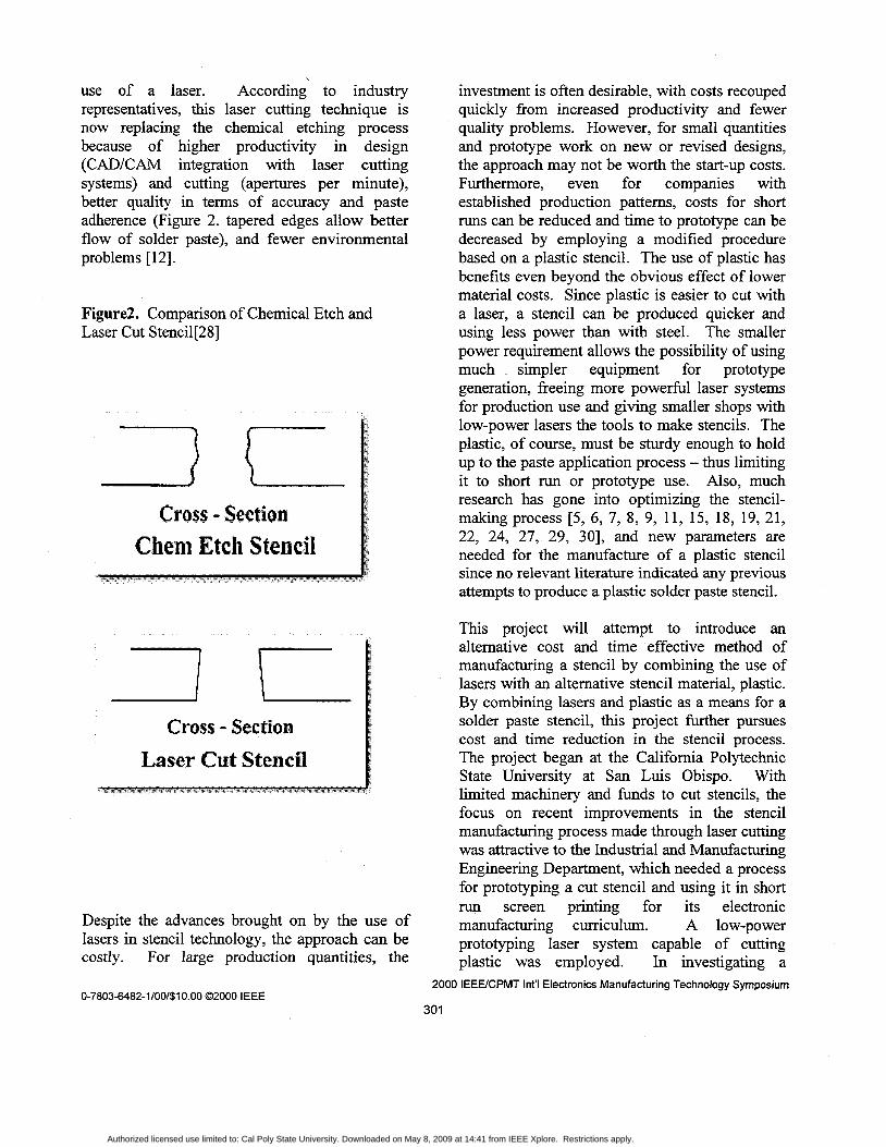
of a laser. According to industry representatives, this laser cutting technique is now replacing the chemical etching process because of higher productivity in design (CAD/CAM integration with laser cutting systems) and cutting (apertures per minute), better quality in terms of accuracy and paste adherence (Figure 2. tapered edges allow better flow of solder paste), and fewer environmental problems [12].
Figure2. Comparison of Chemical Etch and Laser Cut Stencil[28]
Cross I Section Chem Etch Stencil
crass - Section Laser Cut S t e ~ d
Despite the advances brought on by the use of lasers in stencil technology, the approach can be costly. For large production quantities, the
investment is often desirable, with costs recouped quickly from increased productivity and fewer quality problems. However, for small quantities and prototype work on new or revised designs, the approach may not be worth the start-up costs. Furthermore, even for companies with established production patterns, costs for short runs can be reduced and time to prototype can be decreased by employing a modified procedure based on a plastic stencil. The use of plastic has benefits even beyond the obvious effect of lower material costs. Since plastic is easier to cut with a laser, a stencil can be produced quicker and using less power than with steel. The smaller power requirement allows the possibility of using much simpler equipment for prototype generation, freeing more powerfbl laser systems for production use and giving smaller shops with low-power lasers the tools to make stencils. The plastic, of course, must be sturdy enough to hold up to the paste application process -thus limiting it to short run or prototype use. Also, much research has gone into optimizing the stencil- making process [5, 6, 7, 8, 9, 11, 15, 18, 19, 21, 22, 24, 27, 29, 301, and new parameters are needed for the manufacture of a plastic stencil since no relevant literature indicated any previous attempts to produce a plastic solder paste stencil.
This project will attempt to introduce an altemative cost and time effective method of manufacturing a stencil by combining the use of lasers with an altemative stencil material, plastic. By combining lasers and plastic as a means for a solder paste stencil, this project further pursues cost and time reduction in the stencil process. The project began at the California Polytechnic State University at San Luis Obispo. With limited machinery and funds to cut stencils, the focus on recent improvements in the stencil manufacturing process made through laser cutting was attractive to the Industrial and Manufacturing Engineering Department, which needed a process for prototyping a cut stencil and using it in short run screen printing for its electronic manufacturing curriculum. A low-power prototyping laser system capable of cutting plastic was employed. In investigating a
2000 IEEWCPMT Int'l Electronics Manufacturing Technology Symposium
30 1 0-7803-6482-1/001$10.00 02000 IEEE
Authorized licensed use limited to: Cal Poly State University. Downloaded on May 8, 2009 at 14:41 from IEEE Xplore. Restrictions apply.

procedure, this project will select an appropriate sheet of plastic and employ the prototyping laser to experimentally cut apertures into it. In addition, a set of recommendations will be made for process parameters that facilitate defect-free production of a plastic prototype stencil. Investigations will be made to determine proper aperture size for the stencil, the best solder paste characteristics, and the best printing parameters for depositing the solder.
Conclusions and Recommendations:
This project introduces the idea of using plastic as si media for stencils and shows that this material is a viable solution for the advancement of stencil technology for both educational purposes at Cal Poly and for industry. The electronic manufacturing industry can benefit with faster turnaround for PCB prototyping and design revisions, lower material costs yielding decreased costs for short run productions, and lower capital equipment costs and maintenance.
After completion of this project, it can be concluded that:
1. Plastic copier transparency film is a successful alternative material for stencil manufacture.
2. Solder paste technology has advanced greatly and its use on plastic has no adverse effects.
3. The application of a laser cut plastic solder paste stencil is a resourceful process that may used in electronic manufacturing, particularly for rapid prototyping of SMT boards or short run production.
This project has proved the effective use of the Helisys Rapid Prototyping machine as a resource to nnanufacture adequate solder paste stencils fiom. plastic copier transparency sheets compared to thle time involved process of outsourcing and chemical etching. Successful test results were indicated from experimental printing through the
laser cut plastic stencils usjng the ESP 566 solder paste.
Further progress of tihis plastic stencil accomplishment can be Icamed out with two additional projects. Continued experimentation with other plastics and solcler pastes can lead to improvement of this project.
Recommendations for the implementation and use of a plastic solder paste: stencil include:
1. Verify the proper aperture ratio for printability of solder paste through stencil.
2. The orientation of the stencil should be aligned with the squeegee print direction stroking along the axis of the majority of longer pad dimensions and perpendicular to smaller pad widths.
3. To print results, similar to a metal stencil, use a 1ig;ht pressure and slow speed squeegee stroke leaving a thin film of paste over the stencil. Angling the squeegee towards the print direction may also aid in print quality and paste roll.
4. Peel away plastic solder paste stencil rather than lifting straight off to prevent scooping and shifting of printed paste.
5. If printing repetitiously, or for more than one stroke through the stencil, be sure the underside of the stencil is clean fiom solder paste, otherwise bleeding may result.
References: 1. 3M Corporation, “Material Safety Data
Sheets”, St. Paul, MN, http://www.mmm.com/US/WlSDS/msdsSearch..jhtml
2. Alpha Metals, Jersey City, New Jersey, http://www.alphametals.com --
3. American Acrylics, Chicago, IL, “Cyro Industries Acrylite GI? and Acrylite FF Acjrlic Plastic Sheet Products.”
0-7803-6482-1/001$10.00 02000 IEEE 2000 IEEWCPMT Int‘l Electronics Manufacturing Technology Symposium
302
Authorized licensed use limited to: Cal Poly State University. Downloaded on May 8, 2009 at 14:41 from IEEE Xplore. Restrictions apply.

5.
6.
7.
8.
9.
http://www.americanacrylics.com/cyroffgp.ht m - (1 3 April 1999)
American Acrylics, Chicago, IL, “Other Plastic Sheet Materials.” http://www.americanacrylics.com/othsheet. ht - m (1 3 April 1999)
Anjard, Ronald P., Sr., “Quality solder paste systems for use in microelectronic applications.” Solid State Technology v.26, Oct. 1983, p. 183-189
Bauer, Brian, “Solder Paste and Solder Paste Deposition”, Proceedings of the Technical Program; National Electronic Packaging and Production Conference(NEPCON), 27 Feb - 4 Mar 1, 1994, v.3, p.2329-39
Bouchard, R.N., Proceedings, 1996 International Symposium on Microelectronics, “Using process control techniques to reduce cost and improve quality of thick film printing screens,” 8-10 Oct. 1996, p.585-93
Breed, S., Proceedings of the Technical Program; National Electronic Packaging and Production Conference, NEPCON West 1998, “Advantages in Intelligent Stencil Printing,” 1-5 March 1998, v.1, p.253-6
Brown, Craig, Proceedings of the Technical Program; National Electronic Packaging and Production Conference(NEPCON), “Advances in Screen Printing Technology,” 27 Feb - 4 Mar 1, 1994, v.3, p.1856-61
10. Capillo, Carmen, SURFACE MOUNT TECHNOLOGY, McGraw-Hill, Inc., 1990
1 1. Coleman, William E., Ross, John M., “Design of stencils for mixed technology SMT/flip chip & through-hole/SMT,” National Electronic Packaging and Production Conference-Proceedings of the Technical Program, Part 1, Feb 23-27 1997 vl p 192- 199
12. DEK Precision Screens Division, United Kingdom, “A Guide to a Good Stencil Specification” http://www.dek.com/screens/articles/gssg/def ault.asu (15 Julv 1999)
13. ESP, “Solder Paste Handling: Frequently Asked Questions”, EFD Inc., Lincoln, RI,
14. Fissell, Jeremy, Central Coast Plastics, 129 Granada, Suite B, (805)544-0344
15. Fleck, Ian, Proceedings of the Technical Program; National Electronic Packaging and Production Conference(NEPCON), “Laser cut stencils control solder volume for no- clean paste printing,” 27 Feb - 4 Mar 1, 1994, v.3, p. 185 1-5
16. GE Structured Products, “Fact and Data Sheets” httu ://www . structureduroduct s. ge . com/uroduc ts/products americas.html(l5 July 1999)
17. Ginsberg, Gerald L., SURFACE MOUNT AND RELATED TECHNOLOGIES, Marcel Dekker, Inc., New York, 1989
18. Hale, E., Pan Pacific Microelectronics Symposium: Proceedings of the Technical Program, “Process control in solder paste printing,” 28-3 1 Jan. 1997, p.449-52
19. Hui, I. K., Ralph, B., “The effects of exposure time on tackiness and rheology of solder paste,” Journal of Engineering Manufacture, Proceedings of the Institution of Mechanical Engineers, Part B, v212, nB7, p.517-524, 1998
20.Hwang, Jennie S . , SOLDER PASTE IN ELECTRONICS PACKAGING, Van Nostrand Reinhold, New York, 1989
2000 IEEUCPMT Int‘l Electronics Manufacturing Technology Symposium 0-78034482-1/00/$10.00 02000 IEEE
303
Authorized licensed use limited to: Cal Poly State University. Downloaded on May 8, 2009 at 14:41 from IEEE Xplore. Restrictions apply.
1. Lee, T.S., Pan Pacific Microelectronics Symposium: Proceedings of the Technical ]Program, “Development of CAD tools for pad and metal mask design in SMT,” 28-31 Jan. ‘I 997, p.55-61
22. Iideen, Jimmy, Proceedings of the Technical Program; National Electronic Packaging and Production Conference(NEPCON), “Printing techniques for Fine Pitch Screen Printing,” 27 Feb - 4 Mar 1, 1994, v.3, p.1862-76
23. Peck, D. J., “Solder Paste in SMT: A Training Perspective,” Electronics industries forum of New England, IEEE, 1997, p. 149- 162
24. Roos-Kozel, Barbara, “Designing solder paste rnaterials to attach surface mounted devices.” Solid State Technology v.26, Oct. 1983, p. 173-178
25. Rowland, Robert, SURFACE MOUNT TECHNOLOGY Supplement, SMT’s Solution for Today, IV, Printing, 1997 p.15- 17
26. Rowland, Robert, Belangia, Paul, APPLIED SURFACE MOUNT ASSEMBLY, Van Nostrand Reinhold, New York, 1993
27. Seery, William, ELECTRONIC PACKAGING AND PRODUCTION, “Stepping through surface mount assembly.”
0-78034482-1/001$10.00 02000 IEEE
v34 n8 Aug 1994, Calhners Publishing Co., Des Plaines, IL p.40-41
28. Southwest Stencil, Tempe, AZ, “10 Solid Reasons for Laser vs. Clhem-etch” http://www.swstencil.com/laser.htm (29 June 1999)
29. Stalneker, S. G., Jr., Wyant, R.. A., “New stencil screen developments for thick film printing.” Solid State Technology v.26, Oct. 1983, p. 141-146
30. Spits, David, SURFACE MOUNT TECHNOLOGY, Accuracy and Repeatability in Solder-Paste Printing, Nov. 1996, p.76-79
31. Wu, Gregory, Rantec,, 1173 Los Olivos Avenue, Los Osos, CA, (805)528-5858
Acknowledgements
Much research, industry help, material procurement, and experimenting provided support for the success of this project, especially to Martin Koch, a valued instructor of the California Polytechnic State University, San Luis Obispo, CA. And also to the generous donations of Gregory Wu of Rantec, Los Osos, CA, and Jeremy Fissell of Central Coast Plastics, San Luis Obispo, CA, who all have made significant contributions in areas discussed in this paper.
2000 IEEWCPMT Int‘l Electronics Manufacturing Technology Symposium
304
2
Authorized licensed use limited to: Cal Poly State University. Downloaded on May 8, 2009 at 14:41 from IEEE Xplore. Restrictions apply.