piezoelectric aluminium nitride thin films by...
TRANSCRIPT
UNIVERSIDAD DE LA REPÚBLICA ORIENTAL DEL URUGUAY
UNIVERSITÉ DE LIMOGES (FRANCE)
CO-ADVISED THESIS
For the degree
DOCTOR EN INGENIERÍA QUÍMICA
de la Facultad de Ingeniería de MONTEVIDEO
DOCTEUR DE L’UNIVERSITÉ DE LIMOGES
Spécialité: Matériaux Céramiques et Traitements de Surface
Gustavo SÁNCHEZ MATHON
February the 12th 2009, Montevideo, Uruguay
PIEZOELECTRIC ALUMINUM NITRIDE
THIN FILMS BY PECVD
Advisors: Aldo BOLOGNA ALLES / Pascal TRISTANT,
Christelle DUBLANCHE-TIXIER
Jury :
President : Prof. Jean Claude LABBE SPCTS, Limoges (France)
Revisors: Prof. Miriam CASTRO UNMDP, Mar del Plata (Argentina)
Prof. Abdou DJOUADI IMN, Nantes (France)
Members: Prof. Ismael PIEDRA-CUEVA FING, Montevideo (Uruguay)
Prof. Enrique DALCHIELE FING, Montevideo (Uruguay)
Dr. Christelle DUBLANCHE-TIXIER SPCTS, Limoges (France)
Prof. Pascal TRISTANT SPCTS, Limoges (France)
Prof. Aldo BOLOGNA ALLES FING, Montevideo (Uruguay)
- 2 -
Acknowledgments
I want to express my sincere gratitude to my thesis advisors, Dr. Aldo Bologna Alles,
Dr. Pascal Tristant and Dr. Christelle Dublanche-Tixier for their friendship and
guidance throughout the course of this work.
I also gratefully acknowledge Dr. Jean Claude Labbe, Dr. Ismael Piedra-Cueva,
Dr. Abdou Djouadi, Dr. Miriam Castro, and Dr. Enrique Dalchiele for serving on my
committee.
I would also like to thank to several members of the SPCTS laboratory at Limoges
for their support: Daniel Tetard, Thérèse Merle, Valérie Coudert, Phillippe Thomas,
Alexandre Boulle, René Guinebretiere, Bernard Soulestin, Fabrice Rossignol, Daniel
Merle and Cédric Jaoul. I would like to give a special acknowledge in this sense to
Hervé Hidalgo.
I want to acknowledge to Jaume Esteve and Joseph Montserrat from the Instituto
de Microelectrónica de Barcelona for their assistance in the cleanroom fabrication of
SAW devices, as well as to Aurelian Crunteanu from X-LIM (Limoges) for his
assistance in the cleanroom fabrication of BAW devices as well in the device
characterizations.
Furthermore, I would like to thank Florent Tetard (Université Paris XIII) as well as
Bassam Abdallah, Eric Gautron, Vincent Fernandez and Jonathan Ahmon (Institut
des Matériaux de Nantes) by their assistance in other characterizations.
I would like to remember the rest of the PhD students at Limoges for their
friendship and their hospitality: Salman Asad, Christophe Cibert, Sébastien
Menessier, Béatrice Sourd, Hamid Belghazi, Claire Tendero, Aure Arcondeguy,
Cécile Marchand, Olivier Tingaud and Fabrice Goutier.

- 3 -
I want to remember Dr. Jean Desmaison, who was my advisor at the beginning of
this work, and acknowledge his wife, Dr. Martine Desmaison-Brut for her friendship
during my stages at Limoges.
I want to express my gratitude to all the institutions that have support this work in
different ways: the University of Limoges, the University of the Republic (Uruguay)
and the French Embassy in Uruguay. Particularly, I want to thank some persons of
these institutions by their special disposition: Gaëlle Peyrat and Graciela Vigo.
Lastly and most importantly, I would like to thank my family. I thank my wife Isabel
and my son Daniel for their role in helping me attain this goal.
- 4 -
Abstract
Polycrystalline aluminum nitride thin films were produced with a microwave-plasma
enhanced chemical vapor deposition technique. The plasma-injector distance, the
substrate temperature and the RF bias were the main variables which allowed
achieving this objective. At the time, it was possible to control the preferential
orientation as <0001> or <1010>, both interesting for piezoelectric applications. The
growth mechanisms that conducted to film microstructure development under
different process conditions were explained, enriched by the comparison with a
physical vapor deposition sputtering technique. The obtained films were
characterized in their piezoelectric performance, including the construction of surface
acoustic wave devices and bulk acoustic wave devices. Adequate piezoelectric
response and acoustic velocities were obtained for <0001> oriented films, while
<1010> oriented films did not show piezoelectric response under the configurations
essayed. An extensive analysis was done in order to explain these behaviors.
Keywords: aluminum nitride, thin films, PECVD, film microstructure, piezoelectricity,
SAW devices, BAW devices.
- 5 -
Resumen
Películas delgadas policristalinas de nitruro de aluminio fueron producidas
empleando una técnica de deposición química en fase vapor asistida por plasma de
microondas. La distancia plasma - inyector, la temperatura de substrato y la
polarización RF del porta-substrato fueron las principales variables que permitieron
alcanzar ese objetivo. Al mismo tiempo, fue posible controlar la orientación
preferencial como <0001> o <1010>, ambas de interés para aplicaciones
piezoeléctricas. Los mecanismos de crecimiento que condujeron al desarrollo de la
microestructura en las diferentes condiciones fueron explicados. Esta explicación fue
enriquecida por la comparación con una técnica de deposición física en fase vapor
por pulverización catódica. Las películas obtenidas fueron caracterizadas en su
desempeño piezoeléctrico, incluyendo la construcción de dispositivos
electroacústicos de onda de superficie y de onda de volumen. Las películas
orientadas <0001> mostraron respuesta piezoeléctrica y velocidad de onda acústica
adecuadas. Por otro lado, las películas orientadas <1010> no mostraron respuesta
piezoeléctrica para las configuraciones ensayadas. Un análisis extenso fue
efectuado para explicar las posibles razones de estos comportamientos.
Palabras clave: nitruro de aluminio, películas delgadas, PECVD, microestructura de
películas delgadas, piezoelectricidad, dispositivos SAW, dispositivos BAW.
- 6 -
Résumé
Des couches minces polycristallines de nitrure d’aluminium ont été produites en
utilisant une technique de dépôt chimique en phase vapeur assisté par plasma
micro-onde. La distance plasma - injecteur, la température du substrat et la
polarisation RF du porte - substrat ont été les principales variables pour arriver à ce
but. Dans un même temps, il a été possible de contrôler l’orientation préférentielle
comme <0001> ou <1010>, intéressantes pour des applications piézoélectriques.
Les mécanismes de croissance qui ont conduit au développement des
microstructures dans les différentes conditions ont été expliqués, la comparaison
avec une technique de dépôt physique en phase vapeur par pulvérisation cathodique
a permis d’enricher la discussion. Les performances piézoélectriques des couches
obtenues ont été caractérisées par construction des dispositifs électroacoustiques
d’onde de surface et d’onde de volume. Les couches orientées <0001> ont montré
une réponse piézoélectrique et une vitesse acoustique adéquates. Par contre, les
couches orientées <1010> n’ont pas montré de réponse piézoélectrique dans les
configurations testées. Une analyse exhaustive a été conduite pour expliquer les
possibles raisons de ces comportements.
Mots-clés : nitrure d’aluminium, couches minces, PECVD, microstructure,
piézoélectricité, dispositifs SAW, dispositifs BAW.
- 7 -
Contents
INTRODUCTION...................................................................................................... 14
Chapter 1.................................................................................................................. 16
PIEZOELECTRIC ALUMINUM NITRIDE THIN FILMS: FUNDAMENTALS AND
STATE OF THE ART ............................................................................................ 16
1.1 Piezoelectricity ............................................................................................ 16
1.1.1 Applications of the piezoelectric effect .................................................. 19
1.1.2 Bulk acoustic wave devices .................................................................. 21
1.1.3 Surface acoustic wave devices ............................................................. 23
1.1.4 Characteristics of piezoelectric film for electro-acoustic devices........... 24
1.1.5 Piezoelectric materials .......................................................................... 27
1.2 Aluminum Nitride ......................................................................................... 29
1.2.1 AlN films for BAW and SAW electro-acoustic devices .......................... 34
1.3 Thin Film Manufacturing Techniques........................................................... 37
1.3.1 Plasma assisted techniques for thin films deposition............................ 38
1.3.2 Plasma assisted techniques for polycrystalline AlN films...................... 41
1.4 Thin Film Growth Mechanisms .................................................................... 44
1.4.1 Development of preferential orientation in AlN thin films....................... 46
1.4.2 Residual stress in thin films .................................................................. 50
1.5 Objectives.................................................................................................... 52
Chapter 2.................................................................................................................. 53
EXPERIMENTAL PROCEDURE .......................................................................... 53
2.1 The MWPECVD technique ......................................................................... 53
2.1.1 The reactor ........................................................................................... 53
2.1.2 The process .......................................................................................... 55
2.1.3 Experimental design ............................................................................. 56
2.2 Film characterization ................................................................................... 57
2.2.1 Chemical composition........................................................................... 58
2.2.2 Microstructure ....................................................................................... 60
2.2.3 Mechanical properties........................................................................... 63
2.2.4 Piezoelectric Characterization............................................................... 64
- 8 -
2.3 Plasma characterization by Optical Emission Spectroscopy (OES) ............ 68
Chapter 3.................................................................................................................. 69
GROWTH OF POLYCRYSTALLINE ORIENTED AlN FILMS............................... 69
3.1 Plasma-injector distance ............................................................................. 70
3.2 RF-bias........................................................................................................ 73
3.3 Substrate temperature................................................................................. 74
3.4 Chamber total pressure ............................................................................... 76
3.5 Injector-substrate distance .......................................................................... 78
3.6 Process time................................................................................................ 80
3.7 Film Substrates ........................................................................................... 80
3.8 Discussion ................................................................................................... 83
Chapter 4.................................................................................................................. 85
OPTMIZATION OF FILM PROPERTIES .............................................................. 85
4.1 Pressure-temperature combined effect ....................................................... 85
4.1.1 Annealing effect .................................................................................... 89
4.1.2 Intrinsic stresses vs. temperature for <0001> oriented films................. 90
4.1.3 Piezoelectric coefficient vs. temperature and pressure......................... 92
4.2 Evolution of film properties with thickness ................................................... 93
4.2.1 Microstructure evolution in film profile................................................... 96
4.2.2 Piezoelectric coefficient vs. thickness ................................................... 99
4.3 Effect of low RF bias potentials ................................................................... 99
4.3.1 Development of thicker films............................................................... 106
4.4 Effect of the H2 addition to the reaction chamber....................................... 108
4.5 Optimal process conditions ....................................................................... 109
4.5.1 Reproducibility of the MWPECVD technique ...................................... 113
4.6 Effect of process parameters on plasma characteristics ........................... 114
4.6.1 Identification of species present in the plasma ................................... 115
4.6.2 Effect of H2 addition ............................................................................ 115
4.6.3 Characterization of process plasmas in optimal conditions................. 117
Chapter 5................................................................................................................ 121
APPLICATION TO ELECTROACOUSTIC DEVICES ......................................... 121
5.1 SAW devices ............................................................................................. 121
5.1.1 Frequency response ........................................................................... 121
- 9 -
5.1.2 Modeled response .............................................................................. 125
5.2 BAW devices ............................................................................................. 127
5.2.1 Frequency response ........................................................................... 128
5.2.2 Modeled response .............................................................................. 128
5.3 Discussion ................................................................................................. 130
Chapter 6................................................................................................................ 134
COMPARISON WITH A PVD TECHNIQUE........................................................ 134
6.1 PVD sputtering .......................................................................................... 134
6.2 Piezoelectric performance ......................................................................... 136
6.3 Discussion ................................................................................................. 139
CONCLUSIONS ..................................................................................................... 142
Future Work............................................................................................................ 147
References ............................................................................................................. 148
Appendix A ............................................................................................................. 163
BAW AND SAW DEVICES ................................................................................. 163
A.1 BAW devices............................................................................................. 163
A.2 SAW devices............................................................................................. 171
Appendix B ............................................................................................................. 178
PIEZOELECTRIC CHARACTERIZATION OF THIN FILMS ............................... 178
B.1 Quasi-static measurements ...................................................................... 178
B.2 Dynamic measurements ........................................................................... 186
Appendix C............................................................................................................. 187
A MODEL OF THE ELECTRIC FIELD UNDER THE ELECTRODES................. 187
C.1 The problem.............................................................................................. 187
C.2 Fundamental Equations............................................................................ 188
C.3 Finite differences method.......................................................................... 188
C.4 Results...................................................................................................... 190
Resumen ejecutivo ................................................................................................. 193
PELÍCULAS DELGADAS PIEZOELECTRICAS DE NITRURO DE ALUMINIO POR
PECVD................................................................................................................ 193
Résumé étendu ...................................................................................................... 205
COUCHES MINCES PIEZOELECTRIQUES DE NITRURE D’ALUMINIUM PAR
PECVD................................................................................................................ 205
- 10 -
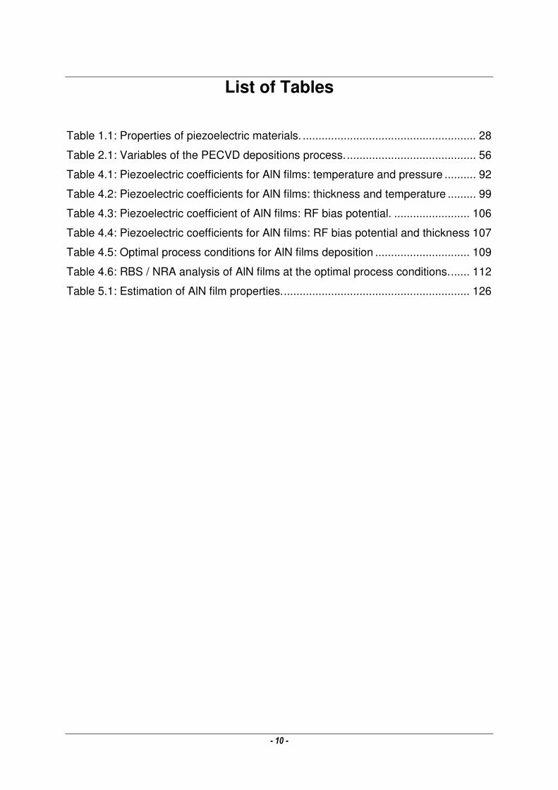
List of Tables
Table 1.1: Properties of piezoelectric materials. ....................................................... 28
Table 2.1: Variables of the PECVD depositions process.......................................... 56
Table 4.1: Piezoelectric coefficients for AlN films: temperature and pressure .......... 92
Table 4.2: Piezoelectric coefficients for AlN films: thickness and temperature ......... 99
Table 4.3: Piezoelectric coefficient of AlN films: RF bias potential. ........................ 106
Table 4.4: Piezoelectric coefficients for AlN films: RF bias potential and thickness 107
Table 4.5: Optimal process conditions for AlN films deposition .............................. 109
Table 4.6: RBS / NRA analysis of AlN films at the optimal process conditions....... 112
Table 5.1: Estimation of AlN film properties............................................................ 126
- 11 -
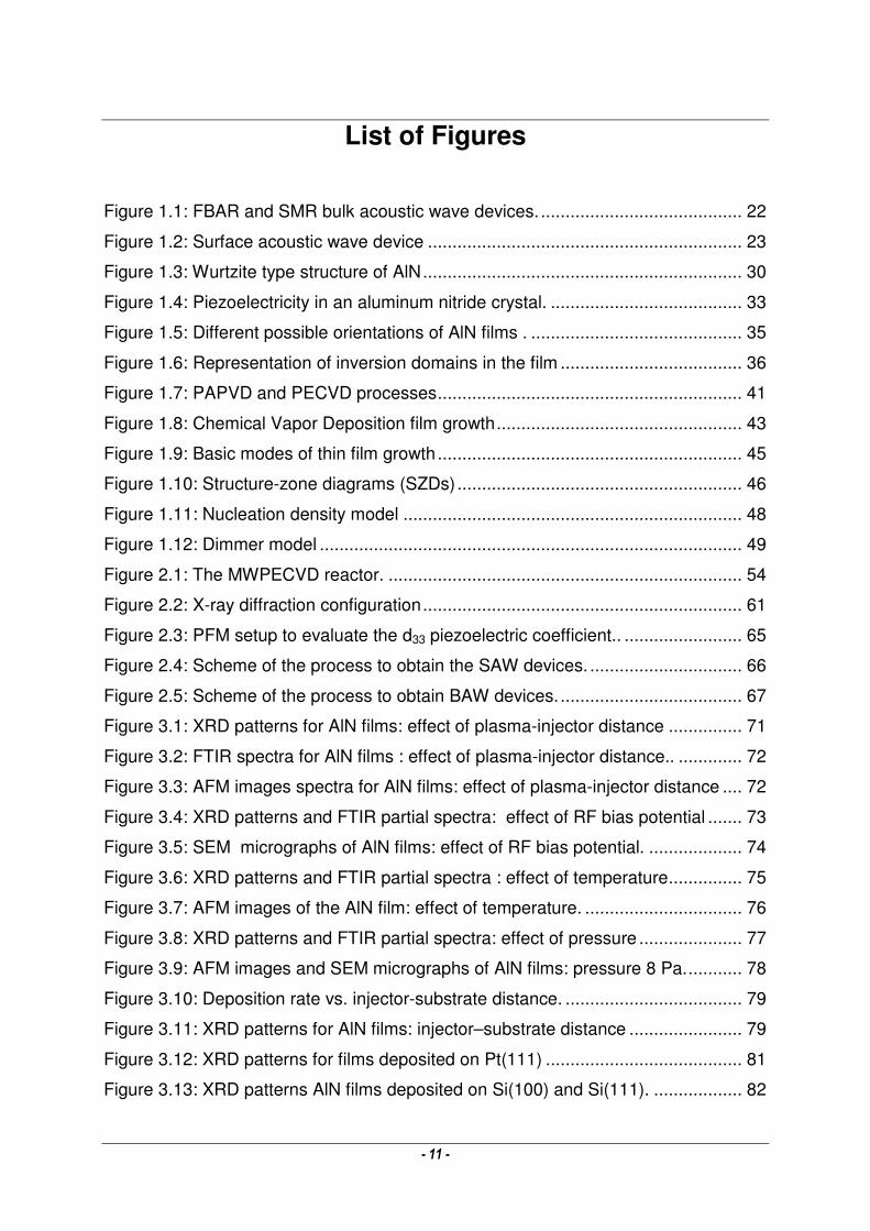
List of Figures
Figure 1.1: FBAR and SMR bulk acoustic wave devices. ......................................... 22
Figure 1.2: Surface acoustic wave device ................................................................ 23
Figure 1.3: Wurtzite type structure of AlN................................................................. 30
Figure 1.4: Piezoelectricity in an aluminum nitride crystal. ....................................... 33
Figure 1.5: Different possible orientations of AlN films . ........................................... 35
Figure 1.6: Representation of inversion domains in the film ..................................... 36
Figure 1.7: PAPVD and PECVD processes.............................................................. 41
Figure 1.8: Chemical Vapor Deposition film growth.................................................. 43
Figure 1.9: Basic modes of thin film growth.............................................................. 45
Figure 1.10: Structure-zone diagrams (SZDs).......................................................... 46
Figure 1.11: Nucleation density model ..................................................................... 48
Figure 1.12: Dimmer model ...................................................................................... 49
Figure 2.1: The MWPECVD reactor. ........................................................................ 54
Figure 2.2: X-ray diffraction configuration................................................................. 61
Figure 2.3: PFM setup to evaluate the d33 piezoelectric coefficient.. ........................ 65
Figure 2.4: Scheme of the process to obtain the SAW devices. ............................... 66
Figure 2.5: Scheme of the process to obtain BAW devices. ..................................... 67
Figure 3.1: XRD patterns for AlN films: effect of plasma-injector distance ............... 71
Figure 3.2: FTIR spectra for AlN films : effect of plasma-injector distance.. ............. 72
Figure 3.3: AFM images spectra for AlN films: effect of plasma-injector distance .... 72
Figure 3.4: XRD patterns and FTIR partial spectra: effect of RF bias potential ....... 73
Figure 3.5: SEM micrographs of AlN films: effect of RF bias potential. ................... 74
Figure 3.6: XRD patterns and FTIR partial spectra : effect of temperature............... 75
Figure 3.7: AFM images of the AlN film: effect of temperature. ................................ 76
Figure 3.8: XRD patterns and FTIR partial spectra: effect of pressure ..................... 77
Figure 3.9: AFM images and SEM micrographs of AlN films: pressure 8 Pa............ 78
Figure 3.10: Deposition rate vs. injector-substrate distance. .................................... 79
Figure 3.11: XRD patterns for AlN films: injector–substrate distance ....................... 79
Figure 3.12: XRD patterns for films deposited on Pt(111) ........................................ 81
Figure 3.13: XRD patterns AlN films deposited on Si(100) and Si(111). .................. 82
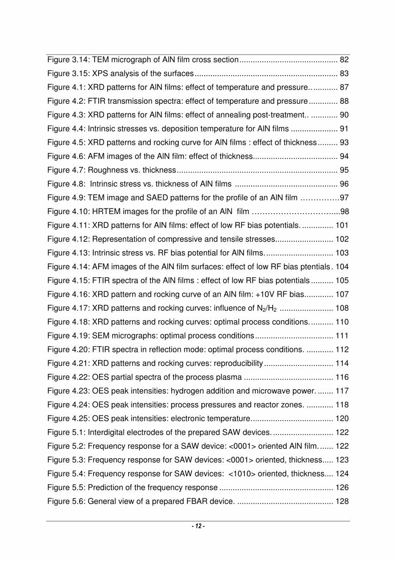
- 12 -
Figure 3.14: TEM micrograph of AlN film cross section............................................ 82
Figure 3.15: XPS analysis of the surfaces................................................................ 83
Figure 4.1: XRD patterns for AlN films: effect of temperature and pressure.. ........... 87
Figure 4.2: FTIR transmission spectra: effect of temperature and pressure............. 88
Figure 4.3: XRD patterns for AlN films: effect of annealing post-treatment.. ............ 90
Figure 4.4: Intrinsic stresses vs. deposition temperature for AlN films ..................... 91
Figure 4.5: XRD patterns and rocking curve for AlN films : effect of thickness......... 93
Figure 4.6: AFM images of the AlN film: effect of thickness...................................... 94
Figure 4.7: Roughness vs. thickness........................................................................ 95
Figure 4.8: Intrinsic stress vs. thickness of AlN films .............................................. 96
Figure 4.9: TEM image and SAED patterns for the profile of an AlN film ……………97
Figure 4.10: HRTEM images for the profile of an AlN film …………………………....98
Figure 4.11: XRD patterns for AlN films: effect of low RF bias potentials. .............. 101
Figure 4.12: Representation of compressive and tensile stresses.......................... 102
Figure 4.13: Intrinsic stress vs. RF bias potential for AlN films. .............................. 103
Figure 4.14: AFM images of the AlN film surfaces: effect of low RF bias ptentials . 104
Figure 4.15: FTIR spectra of the AlN films : effect of low RF bias potentials .......... 105
Figure 4.16: XRD pattern and rocking curve of an AlN film: +10V RF bias............. 107
Figure 4.17: XRD patterns and rocking curves: influence of N2/H2 ........................ 108
Figure 4.18: XRD patterns and rocking curves: optimal process conditions........... 110
Figure 4.19: SEM micrographs: optimal process conditions................................... 111
Figure 4.20: FTIR spectra in reflection mode: optimal process conditions. ............ 112
Figure 4.21: XRD patterns and rocking curves: reproducibility ............................... 114
Figure 4.22: OES partial spectra of the process plasma ........................................ 116
Figure 4.23: OES peak intensities: hydrogen addition and microwave power. ....... 117
Figure 4.24: OES peak intensities: process pressures and reactor zones. ............ 118
Figure 4.25: OES peak intensities: electronic temperature..................................... 120
Figure 5.1: Interdigital electrodes of the prepared SAW devices. ........................... 122
Figure 5.2: Frequency response for a SAW device: <0001> oriented AlN film....... 122
Figure 5.3: Frequency response for SAW devices: <0001> oriented, thickness..... 123
Figure 5.4: Frequency response for SAW devices: <1010> oriented, thickness.... 124
Figure 5.5: Prediction of the frequency response ................................................... 126
Figure 5.6: General view of a prepared FBAR device. ........................................... 128
- 13 -
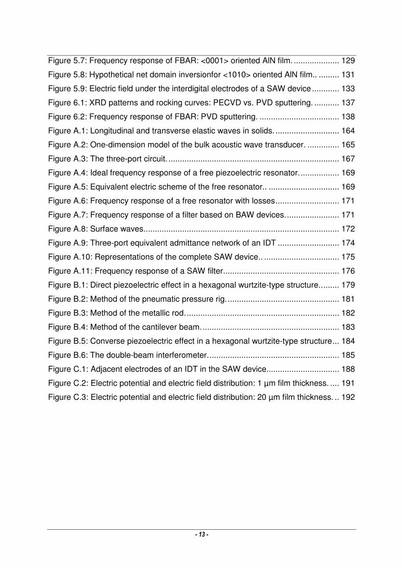
Figure 5.7: Frequency response of FBAR: <0001> oriented AlN film. .................... 129
Figure 5.8: Hypothetical net domain inversionfor <1010> oriented AlN film.. ......... 131
Figure 5.9: Electric field under the interdigital electrodes of a SAW device............ 133
Figure 6.1: XRD patterns and rocking curves: PECVD vs. PVD sputtering. ........... 137
Figure 6.2: Frequency response of FBAR: PVD sputtering. ................................... 138
Figure A.1: Longitudinal and transverse elastic waves in solids. ............................ 164
Figure A.2: One-dimension model of the bulk acoustic wave transducer. .............. 165
Figure A.3: The three-port circuit. ........................................................................... 167
Figure A.4: Ideal frequency response of a free piezoelectric resonator.................. 169
Figure A.5: Equivalent electric scheme of the free resonator.. ............................... 169
Figure A.6: Frequency response of a free resonator with losses............................ 171
Figure A.7: Frequency response of a filter based on BAW devices........................ 171
Figure A.8: Surface waves...................................................................................... 172
Figure A.9: Three-port equivalent admittance network of an IDT ........................... 174
Figure A.10: Representations of the complete SAW device.. ................................. 175
Figure A.11: Frequency response of a SAW filter................................................... 176
Figure B.1: Direct piezoelectric effect in a hexagonal wurtzite-type structure......... 179
Figure B.2: Method of the pneumatic pressure rig.................................................. 181
Figure B.3: Method of the metallic rod.................................................................... 182
Figure B.4: Method of the cantilever beam............................................................. 183
Figure B.5: Converse piezoelectric effect in a hexagonal wurtzite-type structure... 184
Figure B.6: The double-beam interferometer.......................................................... 185
Figure C.1: Adjacent electrodes of an IDT in the SAW device................................ 188
Figure C.2: Electric potential and electric field distribution: 1 µm film thickness. .... 191
Figure C.3: Electric potential and electric field distribution: 20 µm film thickness. .. 192
Piezoelectric Aluminum Nitride Thin Films by PECVD Introduction
- 14 -
INTRODUCTION
At the beginning of the 21st century the world of communications has become
extremely important, and every time the access to information is key to the
development of society. Each day more information is demanded, where the need for
time is a limiting factor in all human activities. An element that has shown a
significant impact on society, in this regard, has been the mobile cell phone, which
has given more independence and security to people everywhere.
The above facts have led to the constant search thereof for higher communication
rates that has derived in the need of higher transmission frequencies. The
transmission and reception of information through electromagnetic waves requires
controlling and filtering frequencies in a precise way. Simultaneously, the use of
portable devices demands the minimization of size as well as energy consumption at
a time that the complexity demand is always on the rise. Then, the integration of the
frequency control technology with Integrated Circuits technology (IC) is a must, since
this combination allows for simpler, more cost effective, manufacturing.
There are a number of ways to attain control over the operating frequency of
communication devices, however frequency control components based on the
piezoelectric effect, and particularly those based on piezoelectric thin films, have
acquire widespread acceptance over the traditional means based on inductive-
capacitive (LC) resonant systems because of their manufacturing compatibility with
IC technology.
BAW (Bulk Acoustic Wave) and SAW (Surface Acoustic Wave) devices based on
piezoelectric thin films have attained crucial importance in this sense. Particularly,
aluminum nitride thin films have been showed as optimal for these applications,
associated mainly with AlN adequate piezoelectric response and high acoustic
velocity. Among the possible techniques to obtain these AlN films, the PECVD
(Plasma Enhanced Chemical Vapor Deposition) shows several advantages to
optimize film microstructure and, simultaneously, it has not been very investigated in
the past for these applications. Consequently, the optimization of a microwave-
Piezoelectric Aluminum Nitride Thin Films by PECVD Introduction
- 15 -
PECVD technique to obtain piezoelectric AlN films for SAW and BAW applications
was conducted in this work.
Therefore, the content of this manuscript is organized as follows:
A general review of the fundamentals and state of the art of piezoelectric
aluminum nitride thin films is presented in chapter 1. Piezoelectricity and
electroacoustic devices are shown in order to establish the film characteristics
desired for these applications, analyze the different possible materials and select the
optimal, i.e. AlN. The general properties of AlN, its piezoelectricity and the specific
needed properties of AlN films for SAW and BAW applications are presented in order
to define precisely the microstructure and additional properties searched. Then, the
different techniques to obtain AlN films are reviewed, and consequently the general
principles of plasma assisted techniques are presented. The advantages of choosing
a microwave - PECVD technique are discussed. Afterward, the general mechanisms
proposed in the past to explain AlN film growth, as well as microstructure and
residual stress development is shown. Finally, based on all the previous information,
the objectives of the work are established.
In chapter 2, the experimental procedure conducted in this work is described,
related with the deposition process and the characterization techniques.
The development of polycrystalline oriented AlN films is shown in chapter 3 and
the optimization of films properties for piezoelectric applications is shown in chapter
4. Different correlations are established between depositions conditions, plasma
characteristics and properties of the obtained films.
The constructions of SAW and BAW devices with the obtained AlN films and the
evaluation of their frequency response are shown in chapter 5.
Finally, a comparison of these films with those obtained with a PVD (Physical
Vapor Deposition) reactive sputtering technique is presented in chapter 6, with a
discussion of the possible growth mechanisms that take place in both cases.
Appendix A, B and C show a general view of the different techniques for a
piezoelectric characterization of thin films, and different models used to analyze the
frequency response of the electroacoustic devices constructed.
Piezoelectric Aluminum Nitride Thin Films by PECVD Fundamentals and State of the Art
- 16 -
Chapter 1
PIEZOELECTRIC ALUMINUM NITRIDE
THIN FILMS: FUNDAMENTALS AND
STATE OF THE ART
1.1 Piezoelectricity
A solid is defined as piezoelectric if it becomes electrically polarized when subjected
to a mechanical stress (direct effect), and becomes mechanically deformed when an
electric field is applied to it (inverse effect). In order to understand this remarkable
phenomenon, the crystal structure of this solid and the symmetry of the crystal lattice
must be taken into account.
The atoms of the crystal lattice share a given electronic density through the bonds
found between them. If the electronic density happens to be spatially non-uniform, a
periodic arrangement of local electric dipoles can be present in the crystal, although
the sum of all the individual dipoles at a given moment should be zero due to their
instantaneous random orientation.
When a mechanical stress is applied to a solid, the elastic strain generated in the
crystal creates changes in the length and/or direction of the bonds between the
individual atoms. This leads to changes either in magnitude and/or in the direction of
the dipoles present in the crystal, and therefore, a net polarization of the lattice may
result. This is the origin of the direct piezoelectric effect, and its presence or absence
in a given crystal is determined by the symmetry of the lattice.
Piezoelectric Aluminum Nitride Thin Films by PECVD Fundamentals and State of the Art
- 17 -
The discovery of the direct piezoelectric effect, by Pierre and Jacques Curie
(1880), followed directly from the established principle that a phenomenon can only
exist in a system having a symmetry that is a sub-group of the characteristic
symmetry of the observed response [1, 2]. Consequently, any asymmetries found in
different phenomena must already exist in the system composed by the crystal
structure plus the stimuli that are causing them to appear.
In the case of the direct piezoelectric effect, an elastic compressive stress applied
to a crystal that gives rise to an electric polarization as a response can only be
observed if the system including the crystal and the compressive stress has an equal
or lower symmetry than the point-group symmetry of the resulting polarization. In
particular, the system comprised of the crystal and the compressive stress cannot
exhibit piezoelectric activity if it contains a center of symmetry. Since applied elastic
stresses are invariably centrosymmetric, therefore, the latter requirement for a
dielectric polarization to be observed as a response must be provided by the crystal
system, thus, centrosymmetric crystals cannot be piezoelectric. This conclusion was
reached by Curie [1], and later confirmed experimentally since 20 of the 21 non-
centrosymmetric classes of crystals are piezoelectric. In particular, for the 432 class,
although it lacks of a symmetry center, the presence of other symmetry elements in
the crystal system precludes the appearance of piezoelectric behavior in this
particular case [1].
Piezoelectricity implies linear coupling between the mechanical and electrical
magnitudes, thus, a set of general equations of state can be derived from basic
thermodynamics in order to describe this phenomenon:
EdTsSE .. += (1.1)
ETdDT .. ε+= (1.2)
where S: strain (m/m), D: electric displacement (C/m2), T: stress (N/m2), E: electric
field (V/m), sE: compliance tensor (m2/N), єT: permittivity tensor (F/m), d:
piezoelectric tensor (m/V).
In order to describe the linear coupling relations between stimuli and responses in
an anisotropic medium, i.e., a crystal [1], tensors must be used to account for all the
Piezoelectric Aluminum Nitride Thin Films by PECVD Fundamentals and State of the Art
- 18 -
different effects, and to express the fact that a certain stimulus applied along one
direction could result in responses in other directions as well.
Vector quantities, as the electric displacement and the electric field, are properly
described by using three components as a first rank tensor with 31 components.
These two quantities must be equated by the dielectric permittivity, a second rank
tensor (32 components) which is a nine component matrix. Since the strain is a
second rank tensor, thus it is related with the electric field by the piezoelectric tensor,
a third rank tensor with, in principle, 27 components. In a similar fashion, the electric
displacement and the stress are equated by a third rank tensor. Furthermore, the
strain and the stress, both second rank tensors are related by a four rank tensor (34
components), the elastic compliance.
Symmetry considerations related to the intrinsic nature of tensor quantities reduce
the number of independent components found in each tensor (Sij=Sji, Tij=Tji, sijkl=sjilk,
dijk=dikj, єij=єji), and this also allows for a simplified matrix notation:
ii
EEdTsS .. αβαβα += (1.3)
j
T
ijii ETdD .. εαα += (1.4)
with i,j = 1, 2, 3 and α, β = 1, 2, …6.
Depending of the variables conveniently chosen to be independent, different types
of fundamental relations can be written, where Eq. 1.1 and Eq. 1.2 are presented in
the so called “d-form” in which the stress T and the electric field E have been chosen
as the independent variables.
Other representation commonly used is the so called “e-form” where the strain S
and the electric field E are selected as the independent variables, both of which are
related by cE the stiffness tensor, and by e the piezoelectric tensor. In the latter, the
piezoelectric e-coefficients are related with the d-coefficients by [3]:
E
ii sed αβαβ .= (1.5)
with i = 1, 2, 3 and α, β = 1,2,…6 where sEαβ are the compliance coefficients in
m2/N, diβ and eiα are the piezoelectric coefficients in m/V and C/m2 respectively.
Piezoelectric Aluminum Nitride Thin Films by PECVD Fundamentals and State of the Art
- 19 -
When the symmetry of a particular crystalline structure is considered, the number
of independent components in each particular case associated with the piezoelectric
tensor is further reduced. Furthermore, it can be shown that in general all crystal
properties represented by odd rank tensors must be absent in centrosymmetric
crystals, i.e., piezoelectricity. In the case of a non piezoelectric material, all the
piezoelectric coefficients are zero giving a null piezoelectric tensor, and
consequently, both equations of state become uncoupled.
The parameter known as electromechanical coupling coefficient (K2) is widely
used as an indicator of the energy conversion efficiency of a piezoelectric transducer,
since it expresses the ratio of the stored energy and the supplied energy in either
form, i.e. electrical or mechanical. This coefficient is defined as follows:
TEds
dK
ε
22
= d-form (1.6)
SEec
eK
ε
22
= e-form (1.7)
where the appropriate values of the piezoelectric, elastic, and dielectric coefficients
corresponding to each tensor are selected depending on the propagation direction of
the phenomenon in the crystal [3-5].
1.1.1 Applications of the piezoelectric effect
The technology world is fairly dominated by the use of mechanical and electrical
energies. Since piezoelectricity is the link through which both systems are coupled,
piezoelectric materials have lead to the development of many devices, and it has
great potential in future applications [6].
Piezoelectric materials have been used in traditional applications as
electromechanical transducers and actuators. Just to mention a few, the direct
piezoelectric effect is employed in microphones to convert longitudinal sound
vibrations in air, i.e., the mechanical driving force, to an electrical signal. Similarly, it
has been used in turn table pick-ups to convert wobbles grooved in vinyl records into
electrical signals, as well as passive sonar array sensors, lighters, etc. make use of
the direct effect.
Piezoelectric Aluminum Nitride Thin Films by PECVD Fundamentals and State of the Art
- 20 -
On the other hand, the reverse piezoelectric effect is used in earphones, as well
as in transducers to launch sound waves into liquid media - like echo-sounders,
active sonar devices, ultrasonic cleaning systems, etc., while agile piezoelectric
actuators are used in variable focus camera lenses, electronic watches, etc.
Traditionally, quartz, PZT (lead zirconate titanate), barium and lead titanate have
been used in most of these cases.
The need to have stabilized oscillators to keep radio stations fine tuned to the
allotted broadcast frequency derived in the development of one important application
of piezoelectric materials. Electric resonant circuits formerly used become unstable
for this demanding task, thus they have been substituted by piezoelectric technology.
A piezoelectric crystal cuboid, inserted between two electrodes forming a capacitor,
is connected into a resonant electric circuit, where the circuit electric resonance
frequency will be locked in by the frequency of the mechanical oscillations of the
piezoelectric crystal. The latter, in turn, is determined by the geometric dimensions of
the crystal and the velocity at which acoustic waves travel through the solid. By
putting the crystal in a constant temperature environment, it is possible to maintain a
strict control of its geometric dimensions, and thus precisely controlling the
broadcasting frequency.
Acoustic wave devices based on piezoelectric materials have been used in a wide
variety of applications such as delay lines, oscillators, resonators, sensors, actuators,
acoustic microscopy as well as in specialized military equipment. Research carried
out in the field of microelectromechanical systems (MEMs) devices that integrate
electrical and mechanical systems on a semiconductor substrate, led to the
development of microsensors, microactuators, electronic control circuits, and other
devices [7].
At the moment by far the largest market for acoustic wave devices is the
telecommunication industry, primary for wireless communications in mobile cell
phones, wireless telephones and base stations [8, 9]. These portable devices
incorporate acoustic wave filters for precise frequency control that are chiefly based
on surface acoustic wave (SAW) and bulk acoustic wave (BAW) resonator
technology. The most commonly used materials in SAW devices have been bulk
single crystal substrates of quartz, lithium tantalite, and lithium niobate. However, the
Piezoelectric Aluminum Nitride Thin Films by PECVD Fundamentals and State of the Art
- 21 -
enormous growth in communication systems has made frequency control in the
low/medium GHz range, i.e. the microwave region, a key issue.
One of the main disadvantages of standard electroacoustic technology in the
microwave region is that it makes use of single crystal piezoelectric materials. The
materials that can be produced in these conditions are rather limited in number, and
in all cases, they are incompatible with Integrated Circuits (IC) technology. Since the
frequency is determined by the device dimensions and the crystal elastic properties,
i.e. the acoustic velocity, for a given material the only available way to increase the
operating frequency, is to reduce the device dimensions. The latter has inherently
associated physical limits as well as a large increase in manufacturing costs.
In the recent years, thin piezoelectric films have been developed to extend the
application range of electromechanical SAW and BAW devices to increasingly higher
frequencies. The manufacturing of SAW devices employing materials with high
acoustic wave velocities, as well as the development of BAW resonators as Thin Film
Bulk Acoustic Resonators (FBAR) show the most promise to extend piezoelectric
technology to the highest frequency bands. In order to obtain these devices,
piezoelectric thin films with high uniformity and controlled properties must be grown
over relatively large substrates. Additionally, the greatest potential of using thin films
is that they open the door to the possibility of integrating the traditionally incompatible
IC with electro-acoustic technologies.
1.1.2 Bulk acoustic wave devices
The core of a BAW device is a BAW resonator that consists of an acoustic cavity-
i.e., a piezoelectric film- that is enclosed on both sides by metal electrodes in a
sandwich configuration. This structure is acoustically insulated from the supporting
substrate either by creating a gap between the bottom electrode and the substrate, a
configuration known as a membrane resonator or Film Bulk Acoustic Resonators
(FBAR), or by incorporating in this position a Bragg reflector known as a Solidly
Mounted Resonator (SMR) (see Fig. 1.1) [10,11].
The aforementioned devices operate under the general principle by which a series
of mechanical resonant frequencies of vibration in the piezoelectric film will be
observed when the film characteristic dimension d is an odd number of half
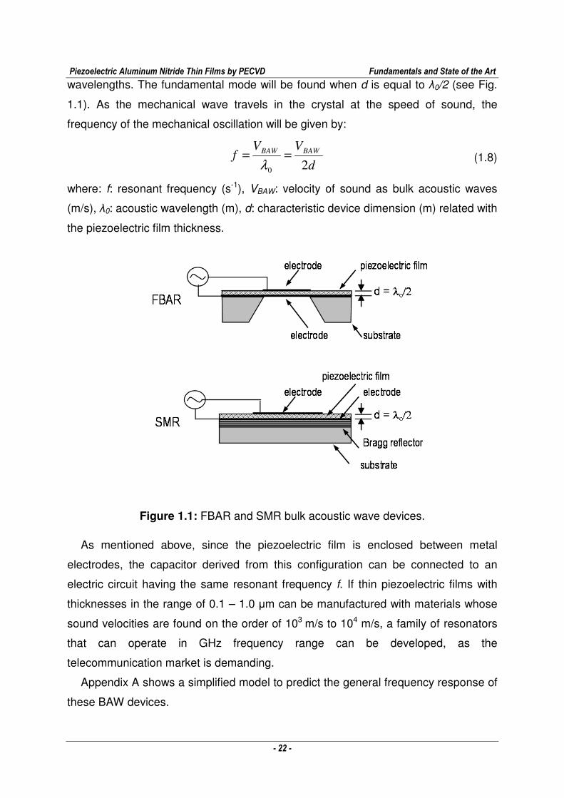
Piezoelectric Aluminum Nitride Thin Films by PECVD Fundamentals and State of the Art
- 22 -
wavelengths. The fundamental mode will be found when d is equal to λ0/2 (see Fig.
1.1). As the mechanical wave travels in the crystal at the speed of sound, the
frequency of the mechanical oscillation will be given by:
d
VVf BAWBAW
20
==λ
(1.8)
where: f: resonant frequency (s-1), VBAW: velocity of sound as bulk acoustic waves
(m/s), λ0: acoustic wavelength (m), d: characteristic device dimension (m) related with
the piezoelectric film thickness.
Figure 1.1: FBAR and SMR bulk acoustic wave devices.
As mentioned above, since the piezoelectric film is enclosed between metal
electrodes, the capacitor derived from this configuration can be connected to an
electric circuit having the same resonant frequency f. If thin piezoelectric films with
thicknesses in the range of 0.1 – 1.0 µm can be manufactured with materials whose
sound velocities are found on the order of 103 m/s to 104 m/s, a family of resonators
that can operate in GHz frequency range can be developed, as the
telecommunication market is demanding.
Appendix A shows a simplified model to predict the general frequency response of
these BAW devices.
Piezoelectric Aluminum Nitride Thin Films by PECVD Fundamentals and State of the Art
- 23 -
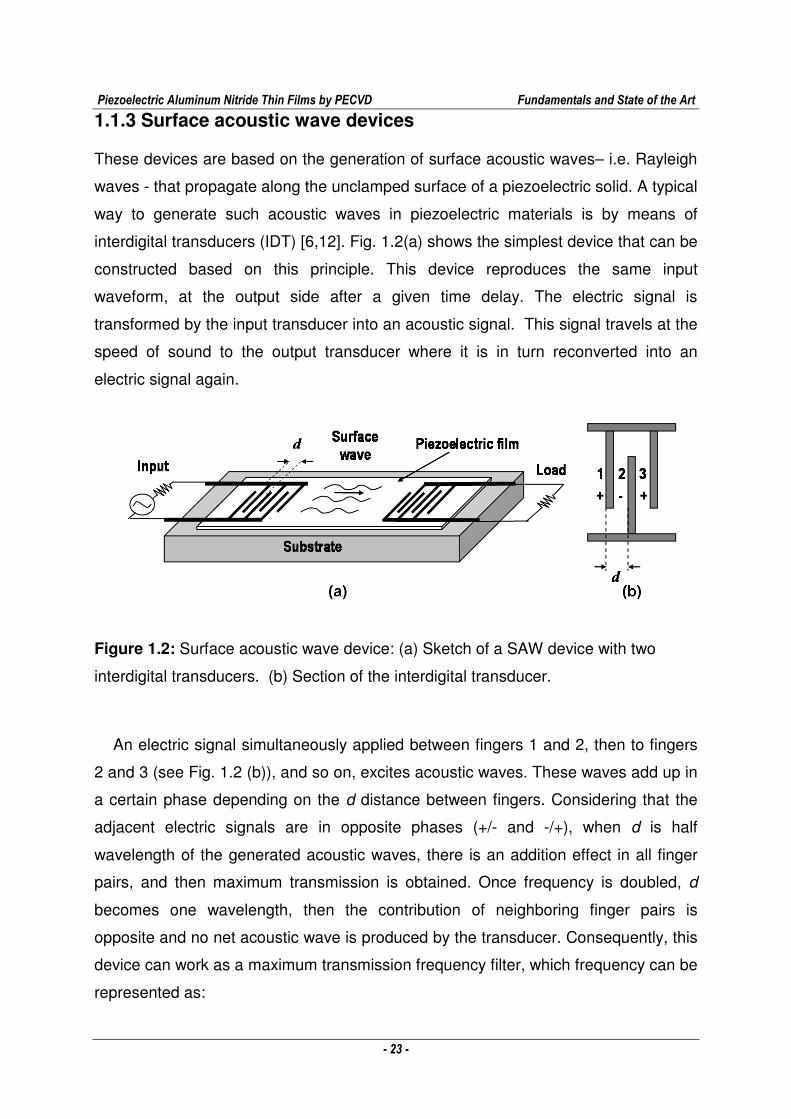
1.1.3 Surface acoustic wave devices
These devices are based on the generation of surface acoustic waves– i.e. Rayleigh
waves - that propagate along the unclamped surface of a piezoelectric solid. A typical
way to generate such acoustic waves in piezoelectric materials is by means of
interdigital transducers (IDT) [6,12]. Fig. 1.2(a) shows the simplest device that can be
constructed based on this principle. This device reproduces the same input
waveform, at the output side after a given time delay. The electric signal is
transformed by the input transducer into an acoustic signal. This signal travels at the
speed of sound to the output transducer where it is in turn reconverted into an
electric signal again.
Figure 1.2: Surface acoustic wave device: (a) Sketch of a SAW device with two
interdigital transducers. (b) Section of the interdigital transducer.
An electric signal simultaneously applied between fingers 1 and 2, then to fingers
2 and 3 (see Fig. 1.2 (b)), and so on, excites acoustic waves. These waves add up in
a certain phase depending on the d distance between fingers. Considering that the
adjacent electric signals are in opposite phases (+/- and -/+), when d is half
wavelength of the generated acoustic waves, there is an addition effect in all finger
pairs, and then maximum transmission is obtained. Once frequency is doubled, d
becomes one wavelength, then the contribution of neighboring finger pairs is
opposite and no net acoustic wave is produced by the transducer. Consequently, this
device can work as a maximum transmission frequency filter, which frequency can be
represented as:
Piezoelectric Aluminum Nitride Thin Films by PECVD Fundamentals and State of the Art
- 24 -
d
VVf SAWSAW
20
==λ
(1.9)
where: f: maximum transmission frequency of the SAW filter (s-1), VSAW: velocity of
sound of surface acoustic waves (m/s), λ0: wavelength (m), d: distance between
adjacent electrodes (see Fig. 1.10(b)) (m).
Many types of SAW devices for different applications have been developed, either
with one or two ports, with or without interdigital reflectors and with different IDT
shape. Among their interesting applications, the described devices have been used
as sensors using the variation of acoustic wave velocity caused by the adsorption of
specific species at the surface between both IDTs.
Since the frequency of SAW devices is determined by the size of IDT fingers,
lately the increase of working frequencies in the microwave domain has led to a
reduction of IDT finger size. By producing IDTs with fingers larger than one
micrometer, traditional lithography processes of microtechnology allow for adequate
productions costs. Smaller sizes need a technological change leading to significant
increases in production costs [13]. Consequently, the acoustic velocity of the
piezoelectric material becomes important in order to attain higher frequencies within
a given finger size.
SAW devices constructed on thin films of piezoelectric materials are employed for
the microwaves domain. And the performance of such devices can be optimized by a
combination of different films with favorable piezoelectric and acoustic
characteristics.
Appendix A shows a simple prediction model of frequency response for a typical
SAW filter.
1.1.4 Characteristics of piezoelectric film for electro-acoustic
devices
Piezoelectric films used in the construction of SAW and BAW devices for
microwave frequencies should have the following characteristics.
Piezoelectric Aluminum Nitride Thin Films by PECVD Fundamentals and State of the Art
- 25 -
a) Piezoelectric coupling
High piezoelectric coupling is required for SAW and BAW applications. Piezoelectric
coupling is expressed by the effective electromechanical coupling coefficient K2
which depends on both the type of material and the propagation direction in the
crystal.
In order to determine the optimal configurations of a given piezoelectric material
for BAW devices, the Christofel equation for the piezoelectric crystal is solved [14].
The results of such equation are represented by the “slowness surfaces” [1, 14],
which show the acoustic wave velocities as function of the propagation directions for
the different wave modes. By comparing scenarios with and without piezoelectric
effect, the directions for which the different modes are piezoelectrically active, i.e.
longitudinal and transverse, are possible to be found out. Thus, the optimal
orientations of the crystal can be chosen by considering the directions of the applied
field. Maximizing the electromechanical coupling coefficient, and avoiding the
development of parasitic modes that could perturb the resonator response can be
reached by this procedure [1, 15].
In the case of SAW devices, the Rayleigh mode guided wave equations and the
corresponding boundary conditions are used for the same purpose as above. These
equations are numerically solved and the evolution of the electromechanical coupling
coefficient and acoustic wave velocity are obtained by progressive rotation of both
the crystal cut and propagation direction [1, 15, 16].
b) High acoustic velocity
Small size devices or high-acoustic velocities are desired in order to allow higher
operation frequencies of devices. Reduction of sizes can imply higher production
costs or lower control of device geometries. Thus, materials with higher acoustic
velocities are desired in order to work at higher frequencies. In a first approach,
acoustic velocity depends on two properties of the material: its mechanical stiffness
constant and its density, according to [1]:
ρ
cV = (1.10)
Piezoelectric Aluminum Nitride Thin Films by PECVD Fundamentals and State of the Art
- 26 -
where: V: acoustic velocity of the excited mode (m/s), c: stiffness constant in the
excited mode (N/m2) when piezoelectrically stiffened (see Appendix 1), ρ : density of
material (kg/m3).
c) Thermal stability of material
The performance of these devices is determined by their ability to remain on the
desired frequency, even under difficult environmental situations [14]. For a BAW
resonator, this frequency depends on the crystal thickness (d) and sound velocity (V)
based on equations 1.8 and 1.10, as follows:
d
c
d
Vfr 2
1
2 ρ== (1.11)
which is valid for the fundamental resonance (first harmonic) of thickness excitation
modes.
All factors in equation 1.11 are temperature-dependent. Therefore, all mutual
dependencies must be taken into account in order determine the optimum crystal cut
and orientation to minimize the effects and reach temperature stability. A derivative
from equation 1.11, is the following:
dT
dd
ddT
d
dT
dc
cdT
df
f
r
r
111
2
11−
−=
ρ
ρ (1.12)
The last term, representing the temperature variation of resonator thickness, is
determined by the material’s linear coefficient of thermal expansion. The middle term,
representing the material’s density temperature variation, generally tends to offset
against the last one. And the first term, represents the variation of stiffness constants
with temperature, which is almost always the largest. Usually, with temperature rise,
stiffness components become softer. Device designers are interested in the
exceptions to this rule, which allow temperature-stable orientations. This is the
reason why quartz is particularly suited for resonators.
d) Low surface roughness
In the case of surface acoustic waves, all energy is concentrated almost within a
wavelength from the surface to the inside (see Appendix 1). Consequently, when
Piezoelectric Aluminum Nitride Thin Films by PECVD Fundamentals and State of the Art
- 27 -
surface roughness is higher than one wavelength, the surface acoustic wave appears
to be unable to pass through. With a rough surface, part of the surface acoustic wave
is converted into a bulk acoustic wave, resulting in large loss for the SAW device [17,
18]. Consequently, surface roughness becomes more critical when the frequency of
the SAW device is higher. Apart from acoustic losses emerging from surface
roughness, there is also the complexity of producing IDTs with appropriate resolution.
e) Mechanical stresses
There should be no excessive internal stress in thin films so as to allow an adequate
geometry and mechanical integrity of the devices.
Other desired characteristics of thin films for piezoelectric devices are: their
adequacy for a deposition process to be feasible, their compatibility with other
microtechnology processes, and chemical stability for their exposure to an
operational environment.
1.1.5 Piezoelectric materials
In general, piezoelectric materials can be classified in two types as follows: polar
piezoelectric materials, with a net dipole moment, and nonpolar piezoelectric
materials, where added dipole moments with different directions result in a null total
moment. Among the 20 non-centrosymmetric piezoelectric classes of crystalline
structures [1, 19] 10 have a permanent net electrical polarization, i.e. they are polar
piezoelectric crystals. Such polar crystals are further classified as ferroelectric and
nonferroelectric.
Many materials have been studied after the discovery of piezoelectric effects in
order to characterize the phenomenon and find applications. Ferroelectric
piezoelectric materials as barium titanate, litium niobiate and litium tantalate, have
shown strong piezoelectric properties. Non ferroelectric piezoelectric materials, such
as quartz have several bulk applications. Quartz is rather popular thanks to its good
temperature stability although its piezoelectric coefficients are not large [20].
Among the ferroelectric piezoelectric thin films, some types have strong
piezoelectric properties. Consequently, they can be applied to
microelectromechanical systems, acoustic wave transducers, sensors and
Piezoelectric Aluminum Nitride Thin Films by PECVD Fundamentals and State of the Art
- 28 -
resonators. The most important are lead titanate zirconate (Pb(ZrxTi1-x)O3), known as
PZT, lead titanate (PbTiO3), usually referred to as PT, and lithium niobate (LiNbO3)
referred to as LN, all of them with a perovskite related structure [19].
In the last decades, the most studied and used non-ferroelectric piezoelectric thin
films have been zinc oxide and aluminum nitride. They are widely used in BAW and
SAW devices, resonators and filters, in spite of their piezoelectric properties weaker
than ferroelectrics [19]. These films have the advantage of low complexity of their
deposition techniques and compatibility with other production processes which
results in their extensive use.
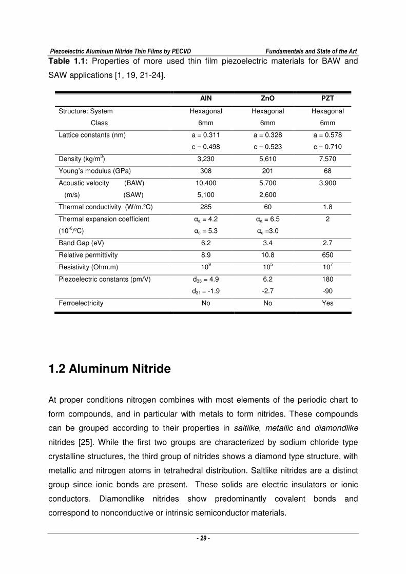
Table 1.1 shows the general properties of AlN, ZnO and PZT, which are the most
widely used materials for SAW and BAW applications.
AlN and ZnO show the lowest piezoelectric coefficients, but enough for these
applications. AlN has the lowest piezoelectric constants, but it shows the highest
propagation velocity of bulk acoustic waves. Also, AIN exhibits the highest surface
acoustic wave velocity, which is enough for manufacturing higher frequency SAW
devices at low cost microtechnology processes. Moreover, AlN shows higher
electrical resistivity, high breakdown voltage, low dielectric loss, high thermal
conductivity and low thermal expansion coefficients. These coefficients imply low
thermal drifts for the devices.
With its higher chemical stability, AlN can be used in humid environments, which is
not possible for the other two materials. At the same time, it can be etched under
standard conditions to allow the production of multiple devices. Finally, AIN does not
introduce contaminants into the CMOS micro-technology process [15], then
becoming completely compatible with CMOS. The last is an additional important
feature of AIN, completely different from the ZnO and PZT.
As a consequence, AlN seems to be the most adequate material for the
applications analyzed here. The following section discusses the general properties
of AlN, its origins and the specific characteristics of AIN films to optimize
performance of piezoelectric devices.
Piezoelectric Aluminum Nitride Thin Films by PECVD Fundamentals and State of the Art
- 29 -
Table 1.1: Properties of more used thin film piezoelectric materials for BAW and
SAW applications [1, 19, 21-24].
AlN ZnO PZT
Structure: System
Class
Hexagonal
6mm
Hexagonal
6mm
Hexagonal
6mm
Lattice constants (nm) a = 0.311
c = 0.498
a = 0.328
c = 0.523
a = 0.578
c = 0.710
Density (kg/m3) 3,230 5,610 7,570
Young’s modulus (GPa) 308 201 68
Acoustic velocity (BAW)
(m/s) (SAW)
10,400
5,100
5,700
2,600
3,900
Thermal conductivity (W/m.ºC) 285 60 1.8
Thermal expansion coefficient
(10-6/ºC)
αa = 4.2
αc = 5.3
αa = 6.5
αc =3.0
2
Band Gap (eV) 6.2 3.4 2.7
Relative permittivity 8.9 10.8 650
Resistivity (Ohm.m) 109 105 107
Piezoelectric constants (pm/V) d33 = 4.9
d31 = -1.9
6.2
-2.7
180
-90
Ferroelectricity No No Yes
1.2 Aluminum Nitride
At proper conditions nitrogen combines with most elements of the periodic chart to
form compounds, and in particular with metals to form nitrides. These compounds
can be grouped according to their properties in saltlike, metallic and diamondlike
nitrides [25]. While the first two groups are characterized by sodium chloride type
crystalline structures, the third group of nitrides shows a diamond type structure, with
metallic and nitrogen atoms in tetrahedral distribution. Saltlike nitrides are a distinct
group since ionic bonds are present. These solids are electric insulators or ionic
conductors. Diamondlike nitrides show predominantly covalent bonds and
correspond to nonconductive or intrinsic semiconductor materials.
Piezoelectric Aluminum Nitride Thin Films by PECVD Fundamentals and State of the Art
- 30 -
The electronic configurations of Al, [Ne]3s23p1, and N, 1s22s22p3, allow the
development of sp3 hybridation of the electronic orbitals to obtain the typical
tetrahedral distribution of the AlN diamondlike structure. The AlN chemical stability
and hardness can be explained by the high energy covalent bonds, in spite of a
certain level of ionic character – i.e. 43% -. Hardness is the reason why AIN is used
for high performance mechanical applications [26].
AIN high acoustic wave velocity is directly related to the high “mechanical stiffness
/ density” rate, which is in turn increased by the high bond energy and low packing
rate of its diamondlike structure - i.e. hexagonal, wurtzite type - (see Figure 1.3 (left)
and Equation 1.10).
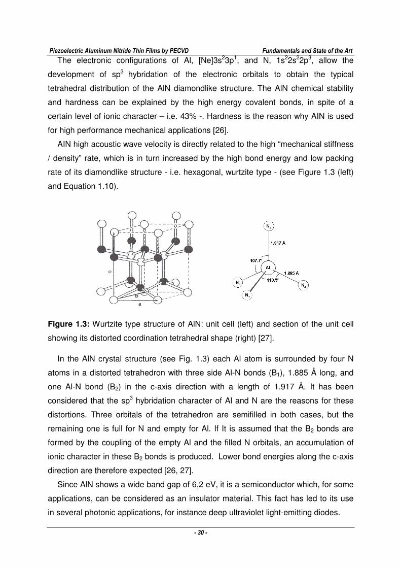
Figure 1.3: Wurtzite type structure of AlN: unit cell (left) and section of the unit cell
showing its distorted coordination tetrahedral shape (right) [27].
In the AlN crystal structure (see Fig. 1.3) each Al atom is surrounded by four N
atoms in a distorted tetrahedron with three side Al-N bonds (B1), 1.885 Å long, and
one Al-N bond (B2) in the c-axis direction with a length of 1.917 Å. It has been
considered that the sp3 hybridation character of Al and N are the reasons for these
distortions. Three orbitals of the tetrahedron are semifilled in both cases, but the
remaining one is full for N and empty for Al. If It is assumed that the B2 bonds are
formed by the coupling of the empty Al and the filled N orbitals, an accumulation of
ionic character in these B2 bonds is produced. Lower bond energies along the c-axis
direction are therefore expected [26, 27].
Since AlN shows a wide band gap of 6,2 eV, it is a semiconductor which, for some
applications, can be considered as an insulator material. This fact has led to its use
in several photonic applications, for instance deep ultraviolet light-emitting diodes.
Piezoelectric Aluminum Nitride Thin Films by PECVD Fundamentals and State of the Art
- 31 -
In the insolent materials thermal conductivity is controlled by phonon transport.
The high “mechanical stiffness / density” rate discussed above contributes to high
thermal conductivity, which is one of the most interesting properties of AlN, which has
led to its use for the support of electronic devices in order to conduct dissipated heat.
With its noncentrosymmetric crystalline structure, wurzite type, AlN is a
piezoelectric material. Apart from being used in BAW and SAW devices associated
with good piezoelectric coupling, high acoustic velocity and thermal stability, other
interesting piezoelectric applications have been developed too. Such is the case of
pressure sensors for combustion engines, where AlN combines the possibility of
maintaining piezoelectric performance at high temperatures (non-ferroelectric), with
chemical and thermal stability [28].
The equations of state corresponding to wurzite-type-structure aluminum nitride
can be expressed in the following full matrix form, based on equations 1.3 and 1.4:
(1.13)
+
=
3
2
1
33
11
11
6
5
4
3
2
1
333131
15
15
3
2
1
.
00
00
00
.
000
00000
00000
E
E
E
T
T
T
T
T
T
ddd
d
d
D
D
D
ε
ε
ε
(1.14)
where there are only three independent piezoelectric coefficients, d33, d31 and d15, for
the piezoelectric tensor.
A simple one-dimensional model, developed to understand the origin of
piezoelectricity and the piezoelectric coefficient in asymmetric ionic crystals, can be
applied to aluminum nitride [1].
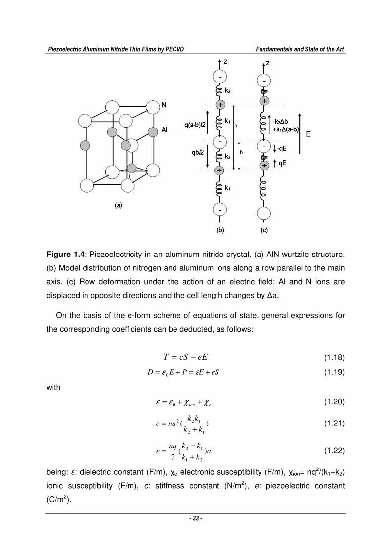
AlN crystal lattice can be envisioned as consisting of successive layers of nitrogen
and aluminum ions (see Fig. 1.4(a)), where ions are repeated along identical rows
+
−
=
3
2
1
15
15
33
31
31
6
5
4
3
2
1
1211
44
44
331313
131112
131211
6
5
4
3
2
1
.
000
00
00
00
00
00
.
)(200000
00000
00000
000
000
000
E
E
E
d
d
d
d
d
T
T
T
T
T
T
ss
s
s
sss
sss
sss
S
S
S
S
S
S
Piezoelectric Aluminum Nitride Thin Films by PECVD Fundamentals and State of the Art
- 32 -
(see Fig 1.4(b)) perpendicularly to the layers. When an external agent, such as a
mechanical stress or electric field is applied perpendicularly to these layers,
considering only one row is sufficient because displacement of all ions in one layer is
the same. Based on the assumption that –q and +q are the effective charges of
nitrogen and aluminum ions linked to each other by springs, and that the closest
neighboring ions are not symmetrically distributed, the springs on either side have
different force constants k1 and k2. The chain is divided into cells, which length is a,
each containing two dipoles with moments q(a-b)/2 and –qb/2, where b is one of the
interatomic distances. The dipole moment of one molecule is then
2
)2.(0
baqp
−= (1.15)
Therefore, the crystal is polar in this case. When at rest, and taking n as the
number of AlN molecules per unit volume, the polarization Po per unit volume is
2
)2.(0
baqnP
−= (1.16)
Under the action of stress, the chain is stretched or compressed, a and b length
changes lead to a polarization change given by
2
)2.(0
baqnPP
∆−∆=∆= (1.17)
This is the direct piezoelectric effect.
In turn, an applied electric field causes the positive and negative ions to be
displaced in opposite directions, so that if (a-b) is increased, then b is reduced (see
Fig 1.4(c)). The different stiffness of each spring results in a deformation. This is the
inverse piezoelectric effect.
Piezoelectric Aluminum Nitride Thin Films by PECVD Fundamentals and State of the Art
- 33 -
Figure 1.4: Piezoelectricity in an aluminum nitride crystal. (a) AlN wurtzite structure.
(b) Model distribution of nitrogen and aluminum ions along a row parallel to the main
axis. (c) Row deformation under the action of an electric field: Al and N ions are
displaced in opposite directions and the cell length changes by ∆a.
On the basis of the e-form scheme of equations of state, general expressions for
the corresponding coefficients can be deducted, as follows:
eEcST −= (1.18)
eSEPED +=+= εε 0 (1.19)
with
eion χχεε ++= 0 (1.20)
)(12
122
kk
kknac
+= (1.21)
akk
kknqe )(
2 21
12
+
−= (1.22)
being: ε: dielectric constant (F/m), χe electronic susceptibility (F/m), χion= nq2/(k1+k2)
ionic susceptibility (F/m), c: stiffness constant (N/m2), e: piezoelectric constant
(C/m2).
Piezoelectric Aluminum Nitride Thin Films by PECVD Fundamentals and State of the Art
- 34 -
Equation 1.22 shows that the existence of piezoelectric effect is exclusively
associated with the asymmetry in the spring constants, since e = 0 when k1 = k2.
Thus, this model explains the origin of piezoelectricity in asymmetric ionic crystals,
and can be applied to aluminum nitride. But in general the piezoelectricity
mechanism is more complex since the piezoelectric effect can also occur in
monoatomic crystals, as tellurium and selenium. In the cases of these crystals, the
electronic polarization is attributed to changes in the electronic distribution.
1.2.1 AlN films for BAW and SAW electro-acoustic devices
The performance of AlN films for piezoelectric application in SAW and BAW electro-
acoustic devices is closely related to the microstructure and compositions of the
films. Although single crystal AlN films would be the ideal option for this application, it
has been demonstrated that preferentially-oriented-polycrystalline films can also
reach adequate performances.
In the case of BAW applications, the electric field is applied perpendicularly to the
substrate in order to produce longitudinal acoustic waves in this direction. As the
piezoelectric effect is maximum in the c-axis direction of the AlN crystal lattice (d33
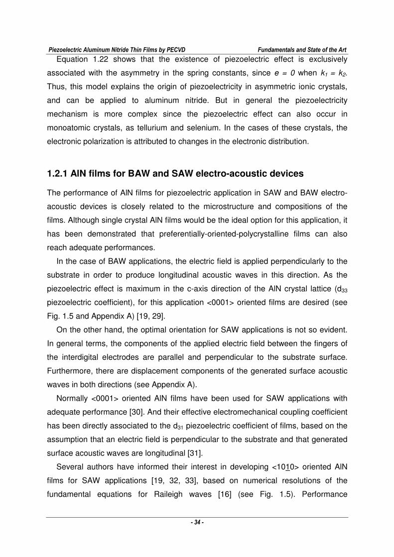
piezoelectric coefficient), for this application <0001> oriented films are desired (see
Fig. 1.5 and Appendix A) [19, 29].
On the other hand, the optimal orientation for SAW applications is not so evident.
In general terms, the components of the applied electric field between the fingers of
the interdigital electrodes are parallel and perpendicular to the substrate surface.
Furthermore, there are displacement components of the generated surface acoustic
waves in both directions (see Appendix A).
Normally <0001> oriented AlN films have been used for SAW applications with
adequate performance [30]. And their effective electromechanical coupling coefficient
has been directly associated to the d31 piezoelectric coefficient of films, based on the
assumption that an electric field is perpendicular to the substrate and that generated
surface acoustic waves are longitudinal [31].
Several authors have informed their interest in developing <1010> oriented AlN
films for SAW applications [19, 32, 33], based on numerical resolutions of the
fundamental equations for Raileigh waves [16] (see Fig. 1.5). Performance
Piezoelectric Aluminum Nitride Thin Films by PECVD Fundamentals and State of the Art
- 35 -
evaluations of SAW devices developed on single-crystal bulk aluminum nitride have
confirmed the advantage of the <1010> orientation [4].
When using the <1010> orientation, the c-axis is parallel to the substrate surface,
then the piezoelectric effect is maximized by the action of the d33 coefficient. In this
simplified consideration these facts have been taken into account: the electric field
component is parallel to the substrate surface and the surface acoustic waves are
longitudinal.
Figure 1.5: Different possible orientations of the AlN film with respect to substrate
surface.
The development of this <1010> orientation has been optimized [32, 34] in some
works, mainly by PVD techniques. However, no evaluation of their performance in
SAW devices has been shown.
Consequently, the orientation grade, or texture, of a polycrystalline AlN film, is an
important parameter associated with the piezoelectric film performance. The
traditional XRD (x-ray diffraction) analysis in the configuration Bragg-Brentano θ/2θ
shows the diffraction response of plans parallel to the substrate surface. Then, the
existence of reflection peaks and their relative intensity are primarily indicative of the
film orientation. For a complete texture evaluation and to quantify the frequency
Piezoelectric Aluminum Nitride Thin Films by PECVD Fundamentals and State of the Art
- 36 -
distribution of orientation within a desired direction range, the “rocking curve”
technique has been developed. The FWHM (full width at half maximum) of the
distribution peak obtained is a direct measurement of dispersion. Many authors have
established a link between the FWHM of the rocking curve and the piezoelectric
performance of <0001> oriented AlN films. They suggest maximal FWHM values for
an acceptable piezoelectric performance, e. g. : 4 - 8º [9, 21, 29, 31].
Moreover, this correlation has been modeled by Lughi [21] by using the AlN
piezoelectric tensor, the transformation of coordinates, and a Gaussian-distributed
analysis. The model results were in accordance with the measurements, mainly for
low FWHM values.
In contrast, recent studies have suggested that it is not possible to exclusively link
the FWHM of the rocking curve with the piezoelectric performance. It has been
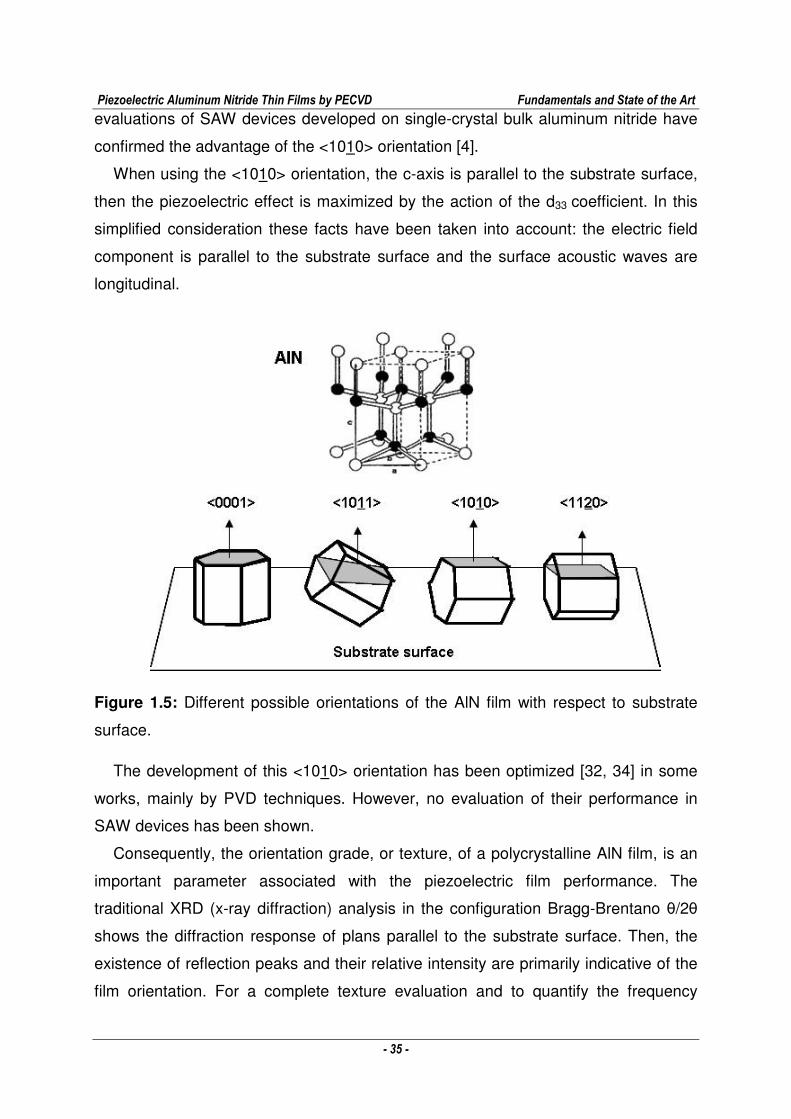
speculated that this absence of correlation is caused by inversion domains or other
unknown microstructure defects [27, 31]. Inversion domains are grains with opposite
crystallographic polarities ([0001] and [0001]), with a resulting negligible net
piezoelectric field (see Figure 1.6). These inversion domains are difficult to identified
but their presence has been shown by some authors [35, 36].
Figure 1.6: Representation of Inversion domains in the film.
Aluminum has high affinity of reaction with oxygen, and this oxygen is usually
present in the deposition process as a consequence of the limited residual vacuum in
the reactor chamber, among other possible reasons. Many works about films
obtained by a Physical Vapor Deposition (PVD) sputtering deposition technique have
been published, in many of them the value of AlN film oxygen impurity is linked to the
FWHM of rocking curves and piezoelectric performance [19, 37, 38]. All of them have
Piezoelectric Aluminum Nitride Thin Films by PECVD Fundamentals and State of the Art
- 37 -
arrived to the conclusion that the increase of oxygen concentration in the film
reduces piezoelectric performance.
The increase of piezoelectric performance has been related to the increase of film
thickness prepared under the same process conditions [39]. However, a favorable
evolution of the crystalline structure going up in the film profile has been observed for
PVD techniques [40].
Acoustic velocities in the range of 10,400 m/s have been determined in BAW
applications. AlN films deposited on Si(100) substrates have shown acoustic
velocities of 5,100 m/s in SAW applications [8, 9, 41-43]. By deposition of AlN on
diamond films [9, 18, 42], it has been possible to attain SAW velocities of
approximately 9,500 m/s, due to the high acoustic velocities of diamond [9, 42].
Surface roughness of the AlN films is particularly critical, as previously discussed,
to reduce the acoustic losses in SAW devices. Values lower than 30 nm have been
informed as adequate for these applications [44].
In summary, in order to optimize the performance of the AlN films for the
piezoelectric applications under study, it is necessary to maximize their crystalline
development and crystallographic texture, in the <0001> or the <1010> directions,
and simultaneously to minimize their roughness, impurity contents and mechanical
residual stress.
The following section analyzes the different possible techniques in order to attain
these objectives. As a result, the most promising option is selected for the research
of this work.
1.3 Thin Film Manufacturing Techniques
Many techniques have been used to obtain AlN films in the past, ranging from MBE
(Molecular Beam Epitaxy) or MOCVD (Metal-organic Chemical Vapor Deposition), to
PVD (Physical Vapor Deposition). Different microstructures have been developed
using these techniques, from single crystal type, to polycrystalline, or eventually
amorphous [19].
Deposition techniques for single crystal films are typically associated with
extremely controlled growth conditions and epitaxy effects on single crystal
Piezoelectric Aluminum Nitride Thin Films by PECVD Fundamentals and State of the Art
- 38 -
substrates. They generally imply very low growth velocities and/or very high
deposition temperatures [45]. Consequently, time consuming operations and
compatibility of other device components with the process temperature are the
reasons why these processes are not practicable for industrial massive applications
in the microelectronic industry.
Then, this research is focused on polycrystalline AlN film techniques, and
particularly in “plasma assisted” techniques, which can be used at lower
temperatures. In the following paragraphs the basis and types of such techniques are
discussed.
1.3.1 Plasma assisted techniques for thin films deposition
A plasma is defined as a quasineutral gas composed of free electrons, ions and
neutral particles exhibiting a collective behavior [46]. In general terms, plasmas can
classified as thermal or cold. In thermal plasmas, all the species are in thermal
equilibrium, being all of them at a common temperature. Conversely, in cold or low
pressure plasmas, free electrons, ions and neutral particles are in independent
thermal equilibriums, with different temperatures for electrons and heavy species.
This particular behavior showed by cold plasmas is explained by the low collision
frequency of species at low pressures and the low energy transfer associated with
the elastic collisions of electrons with heavy species [47, 48].
Cold plasmas are used in film deposition processes with the object of providing the
necessary activation energy for chemical reactions through the inelastic collisions of
free electrons with heavy species. This is possible at a relatively low substrate
temperature, which is related to the heavy species temperature, as a result of the
non-equilibrium condition between electrons and heavy species. An additional effect
of deposition process plasmas is the positive ion bombardment of the treated
surface, before and during the film growth. Such ion bombardment can be used both
for cleaning the substrate surface and controlling the film microstructure.
Appreciable radiations are emitted by this type of plasmas in a wide wavelength
band, including the visible spectrum, by bound-bound, bound-free and free-free
processes of electron energy transitions, as a consequence of the high electronic
temperature. Bound-bound processes correspond to the transition of an electron in
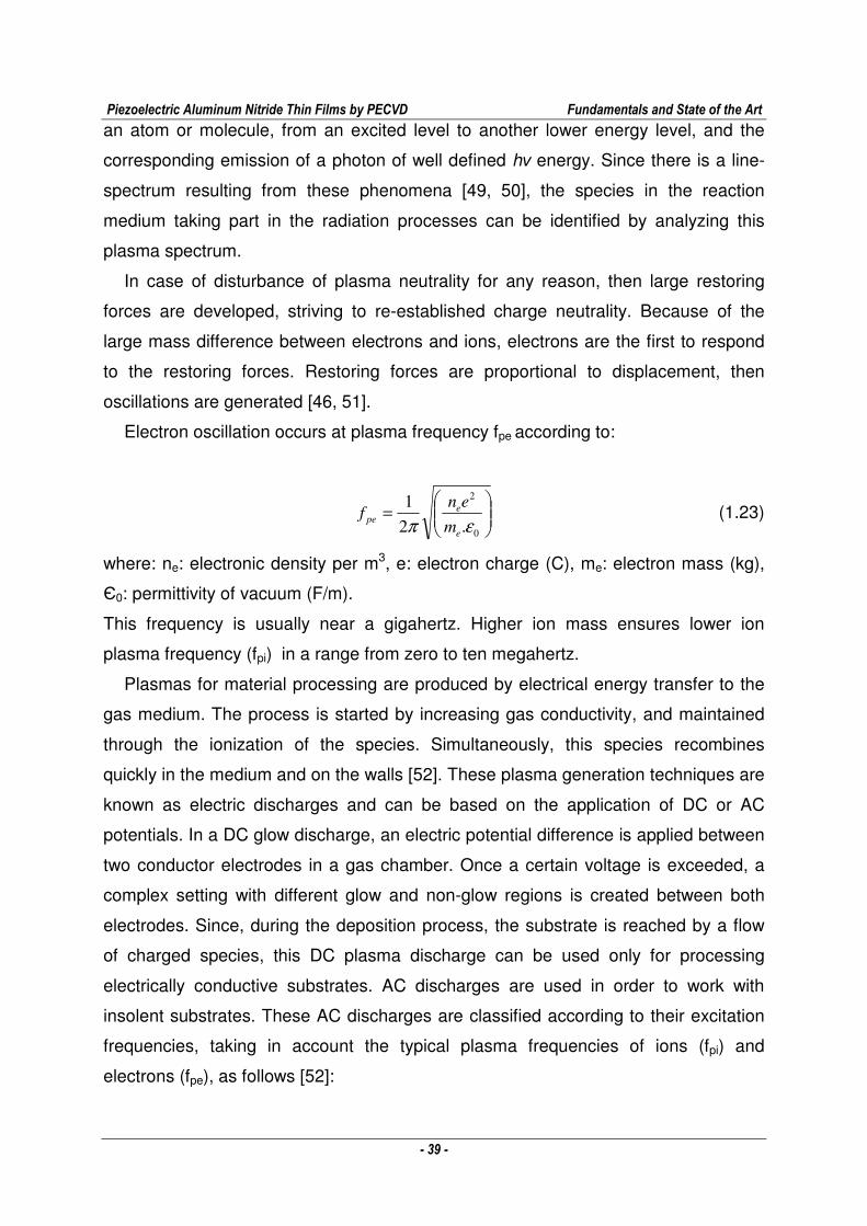
Piezoelectric Aluminum Nitride Thin Films by PECVD Fundamentals and State of the Art
- 39 -
an atom or molecule, from an excited level to another lower energy level, and the
corresponding emission of a photon of well defined hν energy. Since there is a line-
spectrum resulting from these phenomena [49, 50], the species in the reaction
medium taking part in the radiation processes can be identified by analyzing this
plasma spectrum.
In case of disturbance of plasma neutrality for any reason, then large restoring
forces are developed, striving to re-established charge neutrality. Because of the
large mass difference between electrons and ions, electrons are the first to respond
to the restoring forces. Restoring forces are proportional to displacement, then
oscillations are generated [46, 51].
Electron oscillation occurs at plasma frequency fpe according to:
=
0
2
.2
1
επ e
epe
m
enf (1.23)
where: ne: electronic density per m3, e: electron charge (C), me: electron mass (kg),
Є0: permittivity of vacuum (F/m).
This frequency is usually near a gigahertz. Higher ion mass ensures lower ion
plasma frequency (fpi) in a range from zero to ten megahertz.
Plasmas for material processing are produced by electrical energy transfer to the
gas medium. The process is started by increasing gas conductivity, and maintained
through the ionization of the species. Simultaneously, this species recombines
quickly in the medium and on the walls [52]. These plasma generation techniques are
known as electric discharges and can be based on the application of DC or AC
potentials. In a DC glow discharge, an electric potential difference is applied between
two conductor electrodes in a gas chamber. Once a certain voltage is exceeded, a
complex setting with different glow and non-glow regions is created between both
electrodes. Since, during the deposition process, the substrate is reached by a flow
of charged species, this DC plasma discharge can be used only for processing
electrically conductive substrates. AC discharges are used in order to work with
insolent substrates. These AC discharges are classified according to their excitation
frequencies, taking in account the typical plasma frequencies of ions (fpi) and
electrons (fpe), as follows [52]:
Piezoelectric Aluminum Nitride Thin Films by PECVD Fundamentals and State of the Art
- 40 -
a) low frequency (f < fpi < fpe), where the free electrons and ions follow the
oscillations of the electromagnetic field;
b) radiofrequency (fpi < f < fpe), typically 13,56 MHz, where electrons follow the
electromagnetic field oscillations, while ions are sensible to the average temporary
local values of this field;
c) microwave (fpi < fpe ≈ f), where behavior is similar to b), though enhanced.
Radiofrequency discharges are often used in the microelectronic industry. Their
electronic density range is usually 1010 cm-3 and their ions are “frozen” in comparison
with the radiofrequency field. In an oscillation the numbers of lost electrons on the
cathode (substrate holder) and on the anode (chamber walls) are the same, then if
their surfaces are different an auto-polarization voltage (bias) can be generated. This
effect is caused by the different electric impedance of the system for each oscillation
sense and the use of a serie capacitor in the circuit [47]. Thus, the acceleration of
positive ions displacing from plasma to substrate have a specific impact on the film
microstructure.
In the case of microwave discharges, excitation frequency is higher than plasma
frequencies fpi and fpe. As a consequence, electrons and ions are “frozen” in relation
to discharge electromagnetic field. Species distribution in microwave discharges is
not defined by the electronic impact creation processes or by wall recombination lost
processes. Compared with radiofrequency discharges, at equal power density,
average microwave electronic energy is lower, however electronic density is higher
(ne > 1011 cm-3), resulting in dissociation rates above 10%. Consequently, with
microwave discharges, higher thin film deposition rates can be attained using the
higher densities of active species, i.e., electrons and ions [53-55].
Most microwave plasmas for deposition processes are based on “surface wave
technology” [50]. One of the main features of these plasmas is that the maximum
level of electric field is near the dielectric wall of the plasma chamber, and this field’s
minimum level is at the plasma center. The structure known as “surfaguide” is
composed of a dielectric tube (quartz) that keeps the environment and the plasma
chamber apart, and a waveguide around such tube is used to conduct the incident
power from the microwave generator to the plasma. Stable and reproducible plasmas
in large diameter cavities can be generated with this structure. Good
generator/plasma energy transfers and large pressure ranges are possible with this
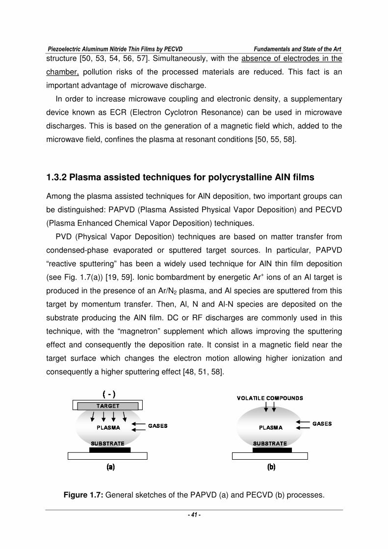
Piezoelectric Aluminum Nitride Thin Films by PECVD Fundamentals and State of the Art
- 41 -
structure [50, 53, 54, 56, 57]. Simultaneously, with the absence of electrodes in the
chamber, pollution risks of the processed materials are reduced. This fact is an
important advantage of microwave discharge.
In order to increase microwave coupling and electronic density, a supplementary
device known as ECR (Electron Cyclotron Resonance) can be used in microwave
discharges. This is based on the generation of a magnetic field which, added to the
microwave field, confines the plasma at resonant conditions [50, 55, 58].
1.3.2 Plasma assisted techniques for polycrystalline AlN films
Among the plasma assisted techniques for AlN deposition, two important groups can
be distinguished: PAPVD (Plasma Assisted Physical Vapor Deposition) and PECVD
(Plasma Enhanced Chemical Vapor Deposition) techniques.
PVD (Physical Vapor Deposition) techniques are based on matter transfer from
condensed-phase evaporated or sputtered target sources. In particular, PAPVD
“reactive sputtering” has been a widely used technique for AlN thin film deposition
(see Fig. 1.7(a)) [19, 59]. Ionic bombardment by energetic Ar+ ions of an Al target is
produced in the presence of an Ar/N2 plasma, and Al species are sputtered from this
target by momentum transfer. Then, Al, N and Al-N species are deposited on the
substrate producing the AlN film. DC or RF discharges are commonly used in this
technique, with the “magnetron” supplement which allows improving the sputtering
effect and consequently the deposition rate. It consist in a magnetic field near the
target surface which changes the electron motion allowing higher ionization and
consequently a higher sputtering effect [48, 51, 58].
Figure 1.7: General sketches of the PAPVD (a) and PECVD (b) processes.
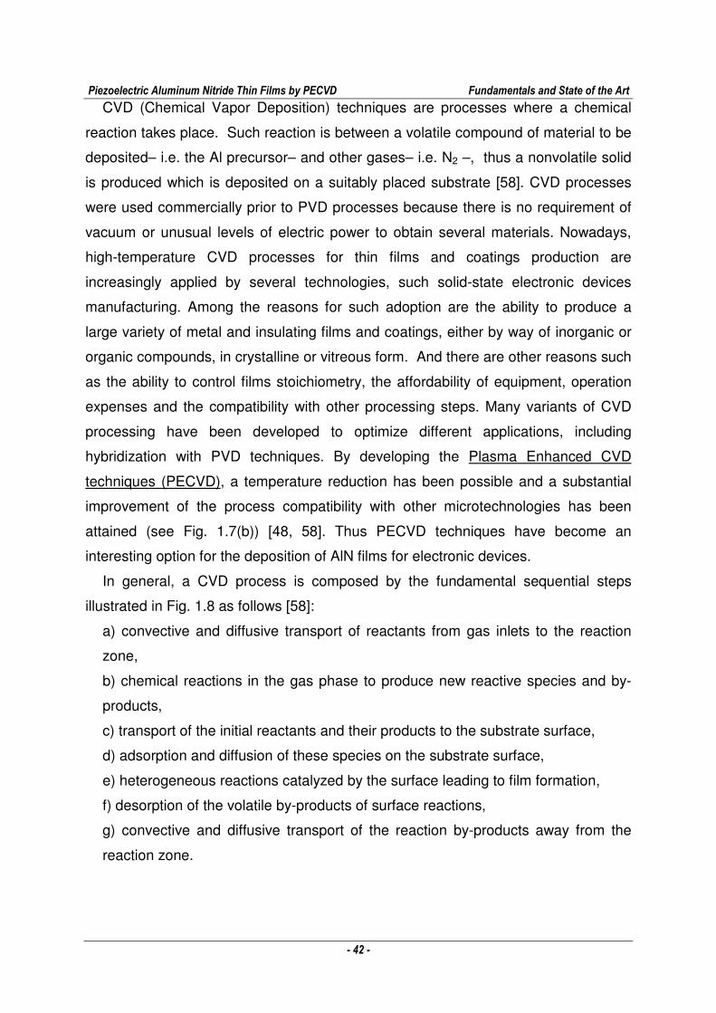
Piezoelectric Aluminum Nitride Thin Films by PECVD Fundamentals and State of the Art
- 42 -
CVD (Chemical Vapor Deposition) techniques are processes where a chemical
reaction takes place. Such reaction is between a volatile compound of material to be
deposited– i.e. the Al precursor– and other gases– i.e. N2 –, thus a nonvolatile solid
is produced which is deposited on a suitably placed substrate [58]. CVD processes
were used commercially prior to PVD processes because there is no requirement of
vacuum or unusual levels of electric power to obtain several materials. Nowadays,
high-temperature CVD processes for thin films and coatings production are
increasingly applied by several technologies, such solid-state electronic devices
manufacturing. Among the reasons for such adoption are the ability to produce a
large variety of metal and insulating films and coatings, either by way of inorganic or
organic compounds, in crystalline or vitreous form. And there are other reasons such
as the ability to control films stoichiometry, the affordability of equipment, operation
expenses and the compatibility with other processing steps. Many variants of CVD
processing have been developed to optimize different applications, including
hybridization with PVD techniques. By developing the Plasma Enhanced CVD
techniques (PECVD), a temperature reduction has been possible and a substantial
improvement of the process compatibility with other microtechnologies has been
attained (see Fig. 1.7(b)) [48, 58]. Thus PECVD techniques have become an
interesting option for the deposition of AlN films for electronic devices.
In general, a CVD process is composed by the fundamental sequential steps
illustrated in Fig. 1.8 as follows [58]:
a) convective and diffusive transport of reactants from gas inlets to the reaction
zone,
b) chemical reactions in the gas phase to produce new reactive species and by-
products,
c) transport of the initial reactants and their products to the substrate surface,
d) adsorption and diffusion of these species on the substrate surface,
e) heterogeneous reactions catalyzed by the surface leading to film formation,
f) desorption of the volatile by-products of surface reactions,
g) convective and diffusive transport of the reaction by-products away from the
reaction zone.
Piezoelectric Aluminum Nitride Thin Films by PECVD Fundamentals and State of the Art
- 43 -
Figure 1.8: Sequence of processes contributing to Chemical Vapor Deposition film
growth [58].
In CVD processes, it is important to point out that mass distribution on substrate
surface is determined mainly by gas flow. Thus, it is possible to easily deal with
special substrate geometries by using a flow distribution adequate design in the
reactor chamber. Conversely, PVD sputtering techniques are highly directional in this
sense, according to the trajectory of the high energy species sputtered from the
target.
In the case of Plasma Enhanced CVD processes, the complex chemistry
associated with the reactive species in the plasma is an additional fact to take into
account. At the same time, the ion bombardment of film surface during the deposition
is an additional parameter that can be controlled in certain configurations, with
important effects on film microstructure. Although some works on the use of PECVD
techniques for AlN films deposition have been published [60-67], very few deal with
the development of piezoelectric characteristics [68].
This concise review of the different possible techniques to obtain AlN films focused
our interest on the growth of piezoelectric AlN films by a Plasma Enhanced Chemical
Vapor Deposition technique; more specifically by using single microwave excitation
to generate the plasma. The reasons for this selection are the following:
- in order to obtain the desired film properties, several parameters can be optimized;
Piezoelectric Aluminum Nitride Thin Films by PECVD Fundamentals and State of the Art
- 44 -
- low directional processes make the deposition on substrates with intricated
geometries possible, such is the case of complex Micro-electromechanical
Systems (MEMs);
- the absence of electrodes in the reactor chamber may reduce film contamination;
- scarce information associated with the characteristics of the AlN films obtained by
this specific technique, and lack of necessary information related to their
piezoelectric performance in electro-acoustic devices;
- comparing films obtained by these techniques with the traditional PVD sputtering
techniques may result in new knowledge on film growth control mechanisms.
The following section contains a review on the general growth mechanisms for thin
films. It is particularly focused on the different theories proposed to explain the
development of preferential crystallographic orientation in AlN films. Finally, some
general theories for the development of residual stresses in thin films are presented.
Such information is taken into account in the following chapters both for the
experimental design and also for the discussion of experimental results obtained.
1.4 Thin Film Growth Mechanisms
Film microstructures are essentially defined by their growth mechanisms. The growth
process consists of a progression of events beginning with condensation of isolated
atomic clusters on a bare substrate, continuing with film thickening due to additional
deposition and resulting in fully developed films. With this process, single-crystal,
polycrystalline or amorphous film microstructures can be developed. Three basic
growth modes have been observed in film developments: island (Volmer - Weber),
layer (Frank - Van der Maerwe), and layer plus island (Stranski - Krastanov), which
are illustrated in Fig. 1.9 [58].
The growth mode for each case is defined by the free surface energies involved:
those associated with film atom bonds or molecule bonds, and those associated with
film species bonds to the substrate. While metal and semiconductor films deposited
on oxide substrates initially form islands, single-crystal epitaxial semiconductor films
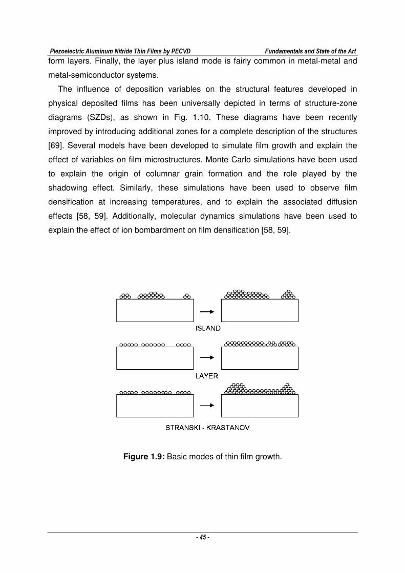
Piezoelectric Aluminum Nitride Thin Films by PECVD Fundamentals and State of the Art
- 45 -
form layers. Finally, the layer plus island mode is fairly common in metal-metal and
metal-semiconductor systems.
The influence of deposition variables on the structural features developed in
physical deposited films has been universally depicted in terms of structure-zone
diagrams (SZDs), as shown in Fig. 1.10. These diagrams have been recently
improved by introducing additional zones for a complete description of the structures
[69]. Several models have been developed to simulate film growth and explain the
effect of variables on film microstructures. Monte Carlo simulations have been used
to explain the origin of columnar grain formation and the role played by the
shadowing effect. Similarly, these simulations have been used to observe film
densification at increasing temperatures, and to explain the associated diffusion
effects [58, 59]. Additionally, molecular dynamics simulations have been used to
explain the effect of ion bombardment on film densification [58, 59].
Figure 1.9: Basic modes of thin film growth.
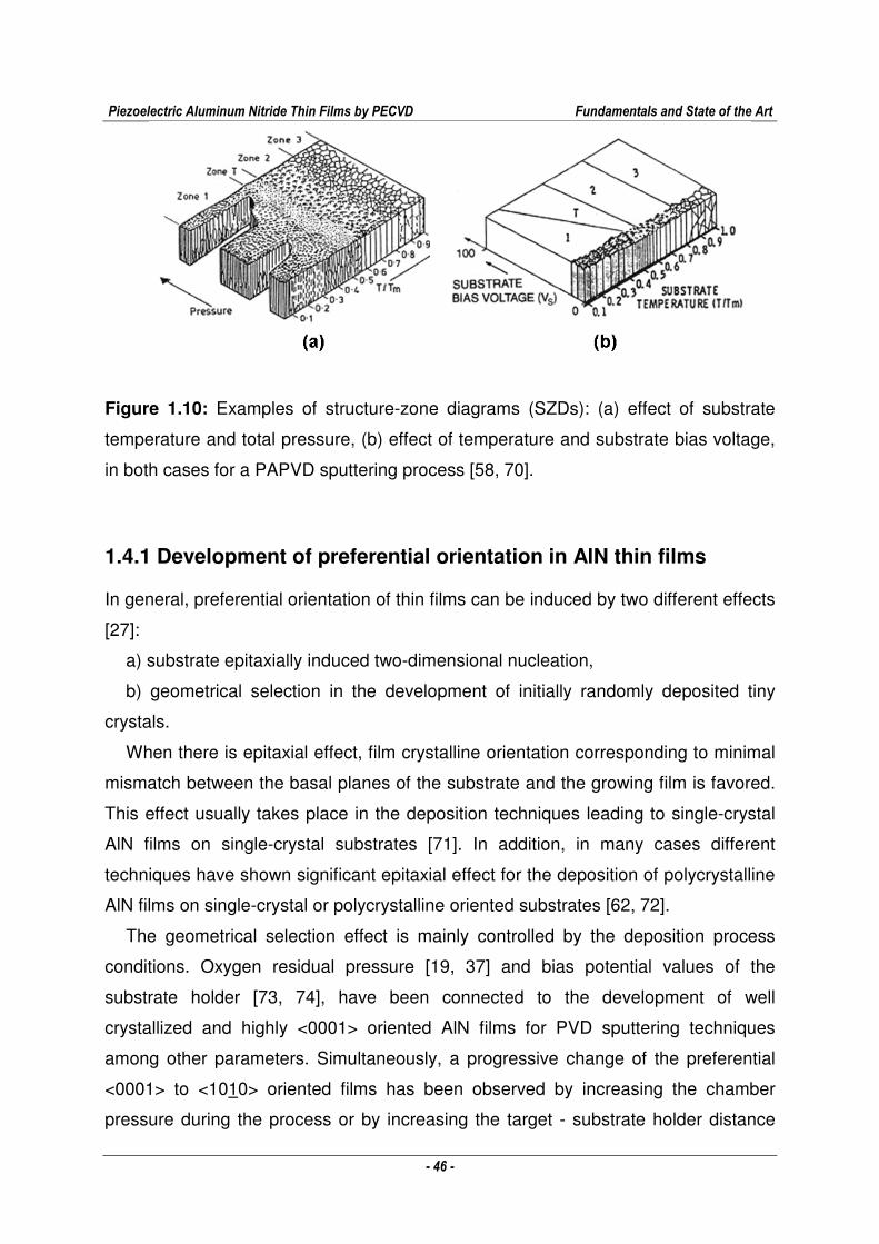
Piezoelectric Aluminum Nitride Thin Films by PECVD Fundamentals and State of the Art
- 46 -
Figure 1.10: Examples of structure-zone diagrams (SZDs): (a) effect of substrate
temperature and total pressure, (b) effect of temperature and substrate bias voltage,
in both cases for a PAPVD sputtering process [58, 70].
1.4.1 Development of preferential orientation in AlN thin films
In general, preferential orientation of thin films can be induced by two different effects
[27]:
a) substrate epitaxially induced two-dimensional nucleation,
b) geometrical selection in the development of initially randomly deposited tiny
crystals.
When there is epitaxial effect, film crystalline orientation corresponding to minimal
mismatch between the basal planes of the substrate and the growing film is favored.
This effect usually takes place in the deposition techniques leading to single-crystal
AlN films on single-crystal substrates [71]. In addition, in many cases different
techniques have shown significant epitaxial effect for the deposition of polycrystalline
AlN films on single-crystal or polycrystalline oriented substrates [62, 72].
The geometrical selection effect is mainly controlled by the deposition process
conditions. Oxygen residual pressure [19, 37] and bias potential values of the
substrate holder [73, 74], have been connected to the development of well
crystallized and highly <0001> oriented AlN films for PVD sputtering techniques
among other parameters. Simultaneously, a progressive change of the preferential
<0001> to <1010> oriented films has been observed by increasing the chamber
pressure during the process or by increasing the target - substrate holder distance
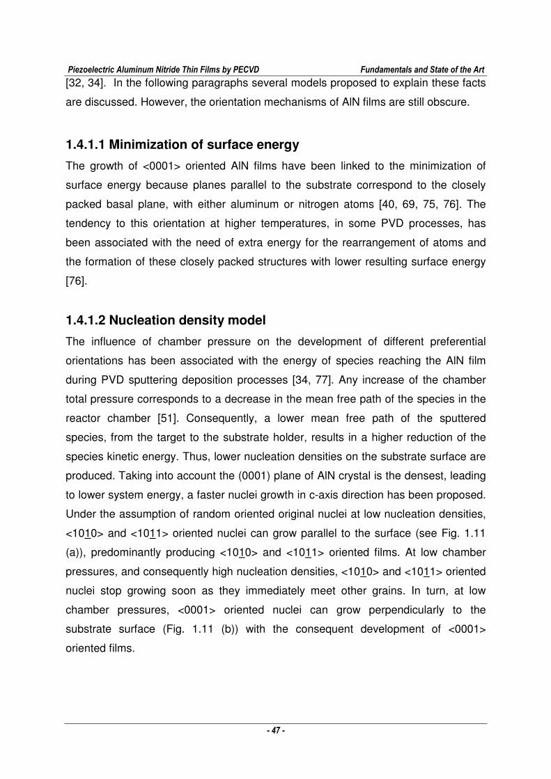
Piezoelectric Aluminum Nitride Thin Films by PECVD Fundamentals and State of the Art
- 47 -
[32, 34]. In the following paragraphs several models proposed to explain these facts
are discussed. However, the orientation mechanisms of AlN films are still obscure.
1.4.1.1 Minimization of surface energy
The growth of <0001> oriented AlN films have been linked to the minimization of
surface energy because planes parallel to the substrate correspond to the closely
packed basal plane, with either aluminum or nitrogen atoms [40, 69, 75, 76]. The
tendency to this orientation at higher temperatures, in some PVD processes, has
been associated with the need of extra energy for the rearrangement of atoms and
the formation of these closely packed structures with lower resulting surface energy
[76].
1.4.1.2 Nucleation density model
The influence of chamber pressure on the development of different preferential
orientations has been associated with the energy of species reaching the AlN film
during PVD sputtering deposition processes [34, 77]. Any increase of the chamber
total pressure corresponds to a decrease in the mean free path of the species in the
reactor chamber [51]. Consequently, a lower mean free path of the sputtered
species, from the target to the substrate holder, results in a higher reduction of the
species kinetic energy. Thus, lower nucleation densities on the substrate surface are
produced. Taking into account the (0001) plane of AlN crystal is the densest, leading
to lower system energy, a faster nuclei growth in c-axis direction has been proposed.
Under the assumption of random oriented original nuclei at low nucleation densities,
<1010> and <1011> oriented nuclei can grow parallel to the surface (see Fig. 1.11
(a)), predominantly producing <1010> and <1011> oriented films. At low chamber
pressures, and consequently high nucleation densities, <1010> and <1011> oriented
nuclei stop growing soon as they immediately meet other grains. In turn, at low
chamber pressures, <0001> oriented nuclei can grow perpendicularly to the
substrate surface (Fig. 1.11 (b)) with the consequent development of <0001>
oriented films.
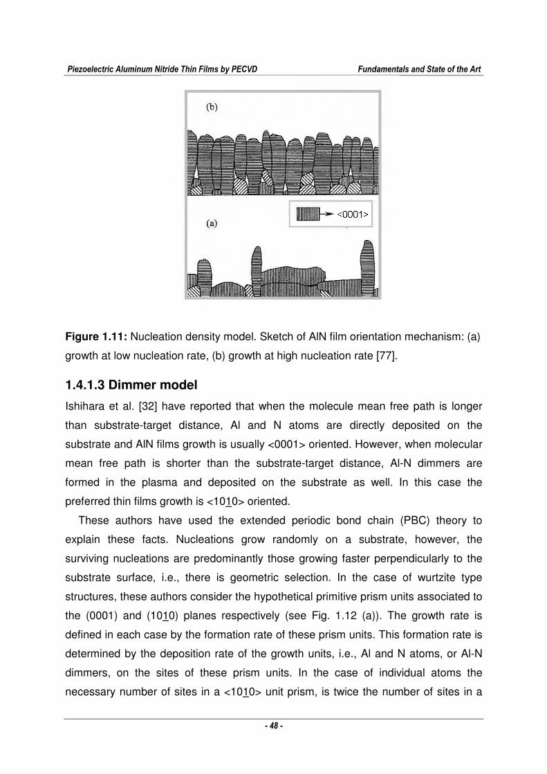
Piezoelectric Aluminum Nitride Thin Films by PECVD Fundamentals and State of the Art
- 48 -
Figure 1.11: Nucleation density model. Sketch of AlN film orientation mechanism: (a)
growth at low nucleation rate, (b) growth at high nucleation rate [77].
1.4.1.3 Dimmer model
Ishihara et al. [32] have reported that when the molecule mean free path is longer
than substrate-target distance, Al and N atoms are directly deposited on the
substrate and AlN films growth is usually <0001> oriented. However, when molecular
mean free path is shorter than the substrate-target distance, Al-N dimmers are
formed in the plasma and deposited on the substrate as well. In this case the
preferred thin films growth is <1010> oriented.
These authors have used the extended periodic bond chain (PBC) theory to
explain these facts. Nucleations grow randomly on a substrate, however, the
surviving nucleations are predominantly those growing faster perpendicularly to the
substrate surface, i.e., there is geometric selection. In the case of wurtzite type
structures, these authors consider the hypothetical primitive prism units associated to
the (0001) and (1010) planes respectively (see Fig. 1.12 (a)). The growth rate is
defined in each case by the formation rate of these prism units. This formation rate is
determined by the deposition rate of the growth units, i.e., Al and N atoms, or Al-N
dimmers, on the sites of these prism units. In the case of individual atoms the
necessary number of sites in a <1010> unit prism, is twice the number of sites in a
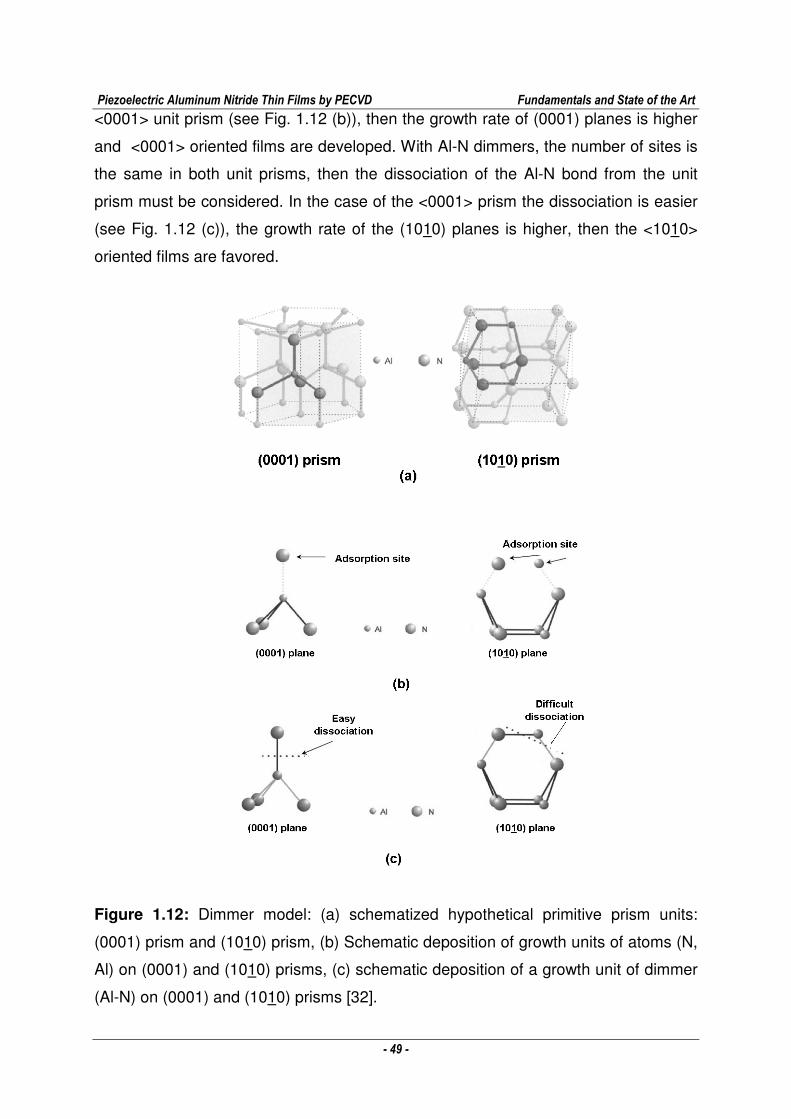
Piezoelectric Aluminum Nitride Thin Films by PECVD Fundamentals and State of the Art
- 49 -
<0001> unit prism (see Fig. 1.12 (b)), then the growth rate of (0001) planes is higher
and <0001> oriented films are developed. With Al-N dimmers, the number of sites is
the same in both unit prisms, then the dissociation of the Al-N bond from the unit
prism must be considered. In the case of the <0001> prism the dissociation is easier
(see Fig. 1.12 (c)), the growth rate of the (1010) planes is higher, then the <1010>
oriented films are favored.
Figure 1.12: Dimmer model: (a) schematized hypothetical primitive prism units:
(0001) prism and (1010) prism, (b) Schematic deposition of growth units of atoms (N,
Al) on (0001) and (1010) prisms, (c) schematic deposition of a growth unit of dimmer
(Al-N) on (0001) and (1010) prisms [32].
Piezoelectric Aluminum Nitride Thin Films by PECVD Fundamentals and State of the Art
- 50 -
Other theories have explained the effect of the mean free path, and established a
connection between the different ionic character of Al-N bonds in the c-axis direction
and the energy of sputtered species reaching the substrate [44].
1.4.2 Residual stress in thin films
When a thin film firmly bonded to a substrate is prepared, any change in length along
the film plane, not exactly matched by an equal change in substrate length, results in
residual stress for such film. Film properties can be affected by the presence of high
stress. Moreover, deformations or catastrophe phenomena, such as fractures or
delaminations, can be produced by excessive residual stresses. As a consequence,
the residual stresses of AlN thin films should be controlled in order to ensure device
integrity and performance.
In overall residual stresses developed in thin films, currently three components can
be distinguished, as follows.
a) Thermal stress, derived from different thermal expansion coefficients of films
and substrates and the difference between deposition temperature and room
temperature.
b) Intrinsic stress, related to the deposition conditions, which may be caused by
incomplete structural-ordering processes during film growth.
c) Extrinsic stress, induced by external factors and resulting from interactions
between deposited material and the environment, e.g. adsorption of water vapor in
porous films.
Many theories have been proposed to explain intrinsic stress development in thin
films, this stress can be either tensile or compressive according to the situation.
The development of tensile stresses in the early stages of polycrystalline film
growth has been explained by Hoffman through the “grain boundary relaxation”
model [58, 78, 79]. This model is based on the idea that crystallites tend to join
together because their individual surface free energies are greater than free energies
when grain boundaries are created by coalescence. As a result, the induced stress is
tensile because the film tries to achieve higher packing. The evolution of stress after
crystallite coalescence during film growth would depend on the availability of
kinetically controlled strain relaxation processes. For high adatom mobility, diffusively
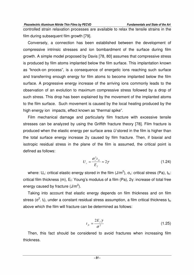
Piezoelectric Aluminum Nitride Thin Films by PECVD Fundamentals and State of the Art
- 51 -
controlled strain relaxation processes are available to relax the tensile strains in the
film during subsequent film growth [79].
Conversely, a connection has been established between the development of
compressive intrinsic stresses and ion bombardment of the surface during film
growth. A simple model proposed by Davis [78, 80] assumes that compressive stress
is produced by film atoms implanted below the film surface. This implantation known
as “knock-on process”, is a consequence of energetic ions reaching such surface
and transferring enough energy for film atoms to become implanted below the film
surface. A progressive energy increase of the arriving ions commonly leads to the
observation of an evolution to maximum compressive stress followed by a drop of
such stress. This drop has been explained by the movement of the implanted atoms
to the film surface. Such movement is caused by the local heating produced by the
high energy ion impacts, effect known as “thermal spike”.
Film mechanical damage and particularly film fracture with excessive tensile
stresses can be analyzed by using the Griffith fracture theory [78]. Film fracture is
produced when the elastic energy per surface area U stored in the film is higher than
the total surface energy increase 2γ caused by film fracture. Then, if biaxial and
isotropic residual stress in the plane of the film is assumed, the critical point is
defined as follows:
γσ
22
≈=f
fcc
cE
tU (1.24)
where: Uc: critical elastic energy stored in the film (J/m2), σc: critical stress (Pa), tfc:
critical film thickness (m), Ef: Young’s modulus of a film (Pa), 2γ: increase of total free
energy caused by fracture (J/m2).
Taking into account that elastic energy depends on film thickness and on film
stress (σ2. tf), under a constant residual stress assumption, a film critical thickness tfc
above which the film will fracture can be determined as follows:
2
2
σ
γf
fc
Et = (1.25)
Then, this fact should be considered to avoid fractures when increasing film
thickness.
Piezoelectric Aluminum Nitride Thin Films by PECVD Fundamentals and State of the Art
- 52 -
1.5 Objectives
As consequence of the information presented in the previous general review, the
objectives of this work are established in the following.
The aim of this work is to produce piezoelectric AlN films with suitable properties
for BAW and SAW electro-acoustic devices using a MWPECVD technique.
Consequently, the object of this work is not only the production of <0001> oriented
AlN films, which are traditionally used for these applications, but also the research of
<1010> oriented films for SAW applications.
The piezoelectric performances of the prepared films are measured by several
techniques, including the construction of electro-acoustic devices.
Film microstructure and compositions are also determined in this work in order to
establish their effect on piezoelectric performance.
Characterizing the process plasma results in additional information for critical
discussion of mechanisms and possibilities provided by the PECVD technique.
Finally, a comparison of the technique discussed in this work with the traditional
PVD sputtering deposition technique for thin films is included.
There is scarce information about the use of this MWPECVD technique for the
development of polycrystalline oriented AlN films and there is no research about
controlling <0001> or <1010> oriented development. Simultaneously, only isolated
information has been published on performance evaluations of electro-acoustic
devices based on <0001> oriented films obtained by this technique.
Last but not least, although interest in developing the <1010> orientation for SAW
devices has been shown in the past, there is no information published about
measuring AlN film device performance for this orientation, regardless of the
deposition technique.
Piezoelectric Aluminum Nitride Thin Films by PECVD Experimental Procedure
- 53 -
Chapter 2
EXPERIMENTAL PROCEDURE
Once the objectives of the work were defined in the previous chapter, based on an
overview of the fundamentals and the state of the art, the experimental procedure
used to conduct the work is presented in the following. The MWPECVD deposition
technique, a general description of the chosen experimental design and the different
methods used to characterize the resulting AlN films are described.
2.1 The MWPECVD technique
2.1.1 The reactor
The reactor consists in a cylindrical chamber- 255 mm diameter and 200 mm height-
constructed in stainless steel, with a quartz glass of the same diameter on top (see
Fig. 2.1). This quartz tube is surrounded by a microwave applicator (280 mm
diameter) opened to the air, which was optimized to obtain the coupling between
microwaves and the plasma through the quartz tube. As the diameter of the quartz is
twice the wavelength of the exciting microwaves- frequency 2,45 GHz, wavelength
127,5 mm-, this arrangement is known as a microwave system with large size
plasma. The microwave energy is produced by a SAIREM 2,000 W generator, and is
propagated through a standard rectangular guide- WR 34, TE10 mode-, to the
cylindrical applicator. Homogeneous plasma is created due to the production of
several modes in the quartz chamber [50]. According stubs placed in the wave guide
are used in order to minimize the reflected power.
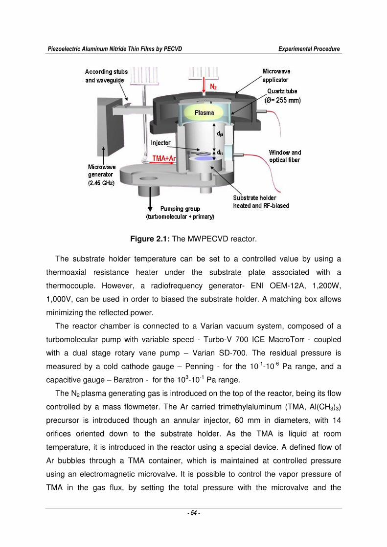
Piezoelectric Aluminum Nitride Thin Films by PECVD Experimental Procedure
- 54 -
Figure 2.1: The MWPECVD reactor.
The substrate holder temperature can be set to a controlled value by using a
thermoaxial resistance heater under the substrate plate associated with a
thermocouple. However, a radiofrequency generator- ENI OEM-12A, 1,200W,
1,000V, can be used in order to biased the substrate holder. A matching box allows
minimizing the reflected power.
The reactor chamber is connected to a Varian vacuum system, composed of a
turbomolecular pump with variable speed - Turbo-V 700 ICE MacroTorr - coupled
with a dual stage rotary vane pump – Varian SD-700. The residual pressure is
measured by a cold cathode gauge – Penning - for the 10-1-10-6 Pa range, and a
capacitive gauge – Baratron - for the 103-10-1 Pa range.
The N2 plasma generating gas is introduced on the top of the reactor, being its flow
controlled by a mass flowmeter. The Ar carried trimethylaluminum (TMA, Al(CH3)3)
precursor is introduced though an annular injector, 60 mm in diameters, with 14
orifices oriented down to the substrate holder. As the TMA is liquid at room
temperature, it is introduced in the reactor using a special device. A defined flow of
Ar bubbles through a TMA container, which is maintained at controlled pressure
using an electromagnetic microvalve. It is possible to control the vapor pressure of
TMA in the gas flux, by setting the total pressure with the microvalve and the
Piezoelectric Aluminum Nitride Thin Films by PECVD Experimental Procedure
- 55 -
temperature of the container fixed by a temperature-controlled water bath. Then, with
the value of the TMA vapor pressure at the selected temperature obtained from the
bibliography, the TMA flow can be calculated as follows [54, 81]:
Ar
v
vTMA F
PP
PF .
−= (2.1)
where: FTMA: TMA flow rate (sccm), FAr: Ar flow rate (sccm), P: total pressure (Pa),
Pv: TMA vapor pressure (Pa).
The distance between the injector and the substrate holder (dis) can be changed.
A modification to the original design of the reactor was introduced in this work in
order to have the possibility of changing the distance between the plasma and the
injector (dpi).
The microwave generator and several reactor parts are cooled by a water circuit in
order to dissipate the produced heat. On the other side the TMA line must be heated
to avoid its condensation before arriving to the reactor chamber.
2.1.2 The process
Substrate wafers of 30 mm x 10 mm were employed as substrates for film deposition.
The wafers were ultrasonically cleaned in ethanol and acetone before placing them in
the reactor chamber. Once closed, the vacuum system of the reactor was switched
on in order to obtain a residual pressure lower than 5 x 10⁻³ Pa in the chamber.
Before the deposition took place, the substrate surface was cleaned in situ using
argon plasma, as will be specified. After pre-heating the substrate holder to the set
temperature at 50°C/min and stabilizing during 15min, AlN films were deposited
using nitrogen plasma in which the trimethylaluminum (TMA) was injected with argon
as carrier gas. Once finished the deposition time, the substrate holder was cooled at
10°/min under vacuum. Finally the chamber was opened to extract the sample once
the temperature of the substrate holder was less than 50°C. Table 2.1 shows the
significant variables of substrate pre-treatment, and AlN film deposition. Variables
selected for optimizing film properties in the experimental design are shown.
The substrate temperatures indicated in the following correspond to the set
temperatures for the substrate holder. As the thermocouple is placed under the
holder plate, certain difference must be expected between the set temperature and
the real substrate temperature. So as to know this difference, an experiment was
Piezoelectric Aluminum Nitride Thin Films by PECVD Experimental Procedure
- 56 -
conducted by putting another thermocouple directly in contact with a substrate
sample simultaneously. The observed results indicated that the real substrate
temperature during the process was approximately 100ºC under the set temperature
in all the used range. Nevertheless, the set temperature is informed in the following,
which corresponds to that effectively measure in the experimental runs. When
theoretical calculations are made, the estimated real temperature is employed.
Table 2.1: Variables of the PECVD deposition process indicating which were chosen
for optimization (*).
Variable Pre-treatment *
AlN film growth
Microwave power (kW) 1.0 1.6 Argon flow rate (sccm(#)) 100 50 Nitrogen flow rate (sccm) 0 125 RF bias potential (V) - 100 - 200 – 0 * Chamber pressure (Pa) 0.8 0.5 – 8 * Processing time (min) 15 0 – 45 * TMA flow rate (sccm) 1 Plasma-injector distance dpi(cm) 3 – 11 * Substrate temperature (°C) 400 – 800 * Injector-substrate distance dis (cm) 4 – 10 * Substrate Si(100), Pt(111), Si (111)*
2.1.3 Experimental design
The experimental work can be divided in three principal stages as follows:
a) Growth of polycrystalline oriented AlN films
Seven different variables were taken into account to produce and optimize the film
properties, i.e. RF bias, the plasma-injector distance, the substrate temperature, the
chamber total pressure, the injector-substrate distance, the process time, and three
different substrates were used. A full fledged experimental design to map out all the
variables and their interactions was excessive to be practical, thus, preliminary work
was carried out to scout the influence of the plasma-injector distance and the RF
bias. After proper values for these two variables were chosen, the rest of the
variables were explored using several levels in each case.
Piezoelectric Aluminum Nitride Thin Films by PECVD Experimental Procedure
- 57 -
b) Optimization of films properties
Additional experimental runs were conducted in order to optimize the performance of
the films in electro-acoustic applications, taking the previous results as reference. A
full fledged experimental design for substrate temperature and total pressure was
done in order to optimize the development of <1010> oriented films. Film thickness
and bias potential were explored separately using several levels in each case in
order to optimize the properties of <0001> oriented films. Finer characterizations of
the microstructure of the films, as well as the measurement of their piezoelectric
performance were introduced at this stage. This was complemented by the process
plasma characterization at different deposition conditions by Optical Emission
Spectroscopy (OES).
c) Application to electro-acoustic devices
SAW electro-acoustic devices with <0001> and <1010> oriented AlN films were
prepared at optimal conditions, as well as BAW electro-acoustic devices for <0001>
oriented films. The frequency response of these devices was measured and models
were used to explain the results obtained in each case.
2.2 Film characterization
The obtained films were characterized in their chemical compositions, microstructure,
mechanical and piezoelectric properties using the following techniques.
Three simple tests were realized immediately after each run in order to have a first
overview of the results:
- Deposited weight: in order to control the deposition rate and its homogeneity on
different positions of the substrate holder.
- Film thickness: part of the sample surface was masked with a resin (“Apiezon”), and
a complete chemical etching of the film using 1 M NaOH solution was made [82].
After eliminating the resin with an adequate solvent the thickness was obtained
through the levels difference measurement with a profilometer.
- Chemical etching: part of the film was etched during 30 seconds at ambient
temperature employing the previous procedure, which allowed obtaining the etch rate
in nm/s.
Piezoelectric Aluminum Nitride Thin Films by PECVD Experimental Procedure
- 58 -
2.2.1 Chemical composition
2.2.1.1 Fourier transform infrared spectroscopy (FTIR)
FTIR spectra were obtained, with a “Perking Elmer Spectrum One” equipment, at the
normal incident angle in transmission mode between 4000 cm-1 and 400 cm-1, with
step 1 cm-1, at 300 K. The substrate spectrum (Si) was used as background. In
addition, spectra were obtained in reflection mode at 30º incident angle. Interference
fringes patterns of FTIR spectra were used to determine the thickness or the
refractive index of the thicker films (> 1 µm) in transmission mode [60].
Because of the transverse character of electromagnetic radiation in conventional
transmission spectroscopy at normal incidence, only AlN transverse optical (TO)
mode vibrations, parallel to the surface, interact with the radiation. In reflection
spectroscopy at 30º, the oblique incidence radiation has components parallel and
perpendicular to the film surface, which can excite both longitudinal optical (LO) and
transverse optical (TO) modes [83].
2.2.1.2 X-ray photoelectron spectroscopy (XPS)
The XPS technique allows obtaining the proportion of elements at a surface, within a
depth of some atoms– i.e. 10 nm. Then, only “the surface” of the films can be directly
analyzed. The XPS measurements of this work were carried out with a Leybold
LHS12 spectrometer (University of Nantes) with MgK radiation (1253.6 eV) as
excitation source. Survey spectra, covering a wide range of energies, have been
taken from -5 to 1,150 eV in binding energy in a constants pass energy mode of 126
eV. Multiregional spectra, for studying narrow energy regions of interest, have been
taken of the predominant photoelectrons peaks at higher resolution using a constant
pass energy mode of 31,5 eV. Multiregional spectra were recorded at 90º take off
angle, i.e. the sample surface was at 90º with respect to the directions of emission of
electrons, detected with a concentric hemispherical energy analyzer. Under these
conditions the Ag 3d5/2 was recorded with 0.93 eV FWHM. The spectrometer was
calibrated using Cu 2p3/2, Au 4f7/2 photoelectrons lines at 832.66 and 84.0 eV,
respectively. The pressure in the analysis chamber was maintained lower than 10-7
Pa. The atomic concentrations were calculated from the photoelectron peak areas
Piezoelectric Aluminum Nitride Thin Films by PECVD Experimental Procedure
- 59 -
using Shirley background subtraction, sensitivity factors provided by the
spectrometer manufacturer and transmission function of this instrument. Recorded
spectra were calibrated in binding energy according to C 1s at 284.7 eV.
2.2.1.3 Rutherford backscattering spectrometry (RBS)
The principle of this technique rests on the study of the elastic scattering between the
cores of an ion incident flux of high energy and the target atoms at rest. Samples
were placed in the analysis chamber under a 2x10⁻⁶ torr vacuum with the zone of
interest aligned with the beam of incident particles. This beam consisted in a 2,0 MeV
He+ ion flux delivered by a Van de Graff electrostatic accelerator, forming an incident
current of 10nA on the target for an analysis surface of some mm². The incident
particles retrodiffused by the cores of the target atoms were detected at 155° from
the initial direction. Thus, a spectrum was obtained, where the particle energy
detected after retro-diffusion was shown in X-coordinate and the number of these
particles seen by the detector was shown in Y-coordinate. This number represented
the detected element concentration at a given depth. Thus, the responses of the
principal components of the sample are normally shown by this type of spectrum, as
steps for massive materials, and as peaks for thin films. While the quantification of
aluminum was possible on these spectra, C, N and O were more delicate to
determine. The superposition of their signals, already weak, with that of the silicon
caused by the substrate was the reason of this fact. Thus, RBS was used to
determine the average proportion of aluminum present in the whole film (ARCANE,
Gradignan, France), and the quantification of C, N, and O was done by the following
technique.
2.2.1.4 Nuclear reaction analysis (NRA)
The principle of the NRA technique consists in creating nuclear reactions between
cores of the atoms in a target and cores of an incident flux of ions with high energy. A
flux of deutons (particles made up of a neutron and a proton) was used (ARCANE,
Gradignan, France), which interacted with the cores of the analyzed atoms (C, N, O)
creating made up cores. Those new cores were disintegrated giving rise to lighter
Piezoelectric Aluminum Nitride Thin Films by PECVD Experimental Procedure
- 60 -
particles which were detected, allowing the quantification of the species initially
present by comparison with reference samples. As these detected light particles had
high energies, they were in a zone of the spectrum where their signal was clearly
distinguished from the background noise. Moreover, a mylar absorbent placed in
front of the detector allowed to stop the incident particles retrodiffused by the
heaviest atoms of the target.
The experimental conditions used for the detection of each element were as follows:
For nitrogen: reaction 14N(d, p)15N with a deutons flow of energy 1.8 MeV, a
current of 50 nA and an integrated charge of 10 µC. A mylar with thickness 20µm
was used as screen. A film of SiN deposited on silicon containing 721 x 1015 at/cm²
of nitrogen was used as standard.
For oxygen: reaction 16O(d, p)17O with a deutons flow of energy 930KeV, a current
of 50 nA and an integrated charge of 20 µC. A mylar with thickness 10µm was used
as screen. A deposit of Al2O3 formed on aluminum containing 912 x 1015 at/cm² of
oxygen was used as standard.
For carbon: reaction 12C(d, p)13C with a deutons flow of energy 1.020 MeV, a
current of 100 nA and an integrated charge of 200 µC. A mylar with thickness 10µm
was used as screen. A silicon substrate implanted with carbon with an amount of
6151 x 1015 at/cm² was used as standard.
2.2.2 Microstructure
2.2.2.1 X-ray diffraction (XRD)
X-ray diffraction (XRD) θ/2θ patterns– i.e. Bragg-Brentano configuration- were
recorded between 15° and 80° (2θ), with a scanning step of 0.05°(2θ), using a D-
5000 diffractometer (Siemens Kristalloflex) equipped with Cu anode and a graphite
back-monochromator. With this arrangement, the incidence and detection angles
relative to the substrate plane were equal during all the measurement (see Fig. 2.2
(a)). Then only information related with the planes parallel to the sample holder was
obtained. Consequently, the crystalline development and a first indication of the
preferential orientation relative to the substrate plane are obtained with this
measurement. The incident angle was offset by 0.5° aiming to reduce the reflections
of the Si (100) substrate between 30° and 40°(2θ). An indication of the average grain
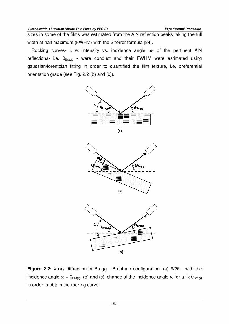
Piezoelectric Aluminum Nitride Thin Films by PECVD Experimental Procedure
- 61 -
sizes in some of the films was estimated from the AlN reflection peaks taking the full
width at half maximum (FWHM) with the Sherrer formula [84].
Rocking curves- i. e. intensity vs. incidence angle ω- of the pertinent AlN
reflections- i.e. θBragg - were conduct and their FWHM were estimated using
gaussian/lorentzian fitting in order to quantified the film texture, i.e. preferential
orientation grade (see Fig. 2.2 (b) and (c)).
Figure 2.2: X-ray diffraction in Bragg - Brentano configuration: (a) θ/2θ - with the
incidence angle ω = θBragg, (b) and (c): change of the incidence angle ω for a fix θBragg
in order to obtain the rocking curve.
Piezoelectric Aluminum Nitride Thin Films by PECVD Experimental Procedure
- 62 -
The textures of some relevant samples were confirmed using a diffractometer with
Debye-Sherrer configuration and automated five - axis substrate holder.
2.2.2.2 Scanning electron microscopy (SEM)
As produced samples and fracture surfaces were observed by scanning electron
microscopy (SEM) using a JEOL JSM-S900LV at 30 kV.
2.2.2.3 Transmission electron microscopy (TEM) – High resolution
TEM (HR TEM) – Selected area electron diffraction (SAED)
Thin specimens for transmission electron microscopy (TEM) were prepared by
cutting, mechanically grinding to ~30-50 µm, dimping (Gatan dimper), and ion-milling
(Gatan PIP) to electron transparency. The observations were made using JEOL TEM
JEM 2010 operating at 200 kV.
The fine structural study of the films was carried out by high resolution
transmission electron microscopy (HRTEM) using a Hitachi HF 2000, and selected
area electron diffraction (SAED) patterns were obtained with an acceleration voltage
of 200 kV (Basam Abdallah, Eric Gautron, University of Nantes).
In the SAED technique, electrons are accelerated by an electrostatic potential in
order to gain the desired energy and wavelength before they interact with the sample
to be studied. The periodic structure of a crystalline solid acts as a diffraction grating,
scattering the electrons in a predictable manner. Working back from the observed
diffraction pattern, the structure of the crystal producing the diffraction pattern can be
deduced [85].
2.2.2.4 Atomic force microscopy (AFM)
Surface morphology of the films was analyzed by atomic force microscopy (AFM)
with a microscope “Molecular Imaging Scanner” operating in tapping mode near 75
kHz under ambient conditions (Valérie Coudert, SPCTS). Silicon tips with a force
constant of 2,8 N/m and a nominal radius of curvature of 20 nm were employed. The
Piezoelectric Aluminum Nitride Thin Films by PECVD Experimental Procedure
- 63 -
Sa roughness coefficient, i.e. the arithmetic mean of the absolute value of the surface
rugosity, was determined by AFM.
2.2.3 Mechanical properties
2.2.3.1 Residual stress
Film residual stresses were estimated by measuring the radius of curvature of 5 mm
x 20 mm x 200 µm Si substrates, after the growth of the AlN films, with a profilometer
and using the Stoney equation [78].
−
−=
12
2 11..
16
1
RRt
tE
film
subs
subs
subsres
υσ (2.2)
where: σres: residual stress ( Pa), Esubs: substrate elastic modulus (Pa), νsubs:
substrate Poisson's ratio, tsubs, tfilm: substrate and film thicknesses (m), R1, R2: initial
and final radius of curvature of the substrate, before and after the deposition (m)
(University of Limoges, Bassam Abdallah- University of Nantes).
2.2.3.2 Nanoindentation: Young’s modulus
Nanoindentation was performed on the films using a Nano Indenter XP™ (MTS Nano
Instruments) with a Berkovich tip in order to determine the Young’s modulus (ENSIL -
SPCTS). The instrument was operated in the continuous stiffness mode allowing
Young’s modulus to be calculated at every data point acquired during the indentation
experiment. This property was evaluated using the Oliver and Pharr's analysis
technique [86, 87]. The indentations were made using a constant nominal strain rate
of 0.05 s−1, a frequency of 45 Hz and harmonic displacement of 2 nm. A Poisson's
ratio of 0.25 was used to calculate the elastic modulus. The average of twenty
indents was taken for each case. The tip correction coefficients were deduced from
indents in fused silica.
2.2.3.3 Intrinsic stress
Thermal stresses of the films were calculated according to [78]:
Piezoelectric Aluminum Nitride Thin Films by PECVD Experimental Procedure
- 64 -
))(()1( adsf
f
f
the TTE
−−−
= ααν
σ (2.3)
where: σthe: thermal stress ( Pa), Ef : Young´s modulus of the film obtained by
nanoindentation (Pa), νf : Poisson´s ratio of the film, αf = 4.1 x 10⁻⁶ K-1 and αs = 2.6 x
10-6 K-1 [88]: thermal expansion coefficients of the film and the substrate, Td and Ta :
deposition and ambient temperatures (K).
By using the previous results (equations 2.2 and 2.3), the intrinsic stresses of the
films (σint) were obtain from:
theres σσσ −=int (2.4)
2.2.4 Piezoelectric Characterization
Film piezoelectric performance was evaluated using three different techniques.
Appendix B shows a general review of commonly applied techniques and
fundamentals of AlN film piezoelectric response.
2.2.4.1 Piezoresponse force microscopy (PFM)
The piezoelectric response of the AlN films was evaluated using an atomic force
microscope adapted to evaluate the piezoelectric coefficient d33 with the inverse
piezoelectric effect (Florent Tetard, University of Paris XIII). Voltage values between
1 and 10 V were applied between the tip and the substrate (see Fig. 2.3), and the
consequent dimensional variations of the piezoelectric film in the vertical directions
were obtained. The equipment was operated in contact mode at 10 kHz, with scan
size of 5 µm, scan rate 1 Hz, and acquisition time of 3 s. The photodiode potential
(mV) was calibrated to nm displacement.
The effective piezoelectric coefficient in the z direction, dzz, was obtained from the
slope of the displacement vs. applied voltage plot. Since the film is clamped to the
substrate, this substrate constrains the in-plane contraction and expansion of the
film. Then, the following equation was applied in order to obtain the piezoelectric
coefficient of the free sample, d33 [29, 89-91]:
EE
E
zzss
sdd
E
Sd
1211
133133
3
3 2+
−== (2.5)
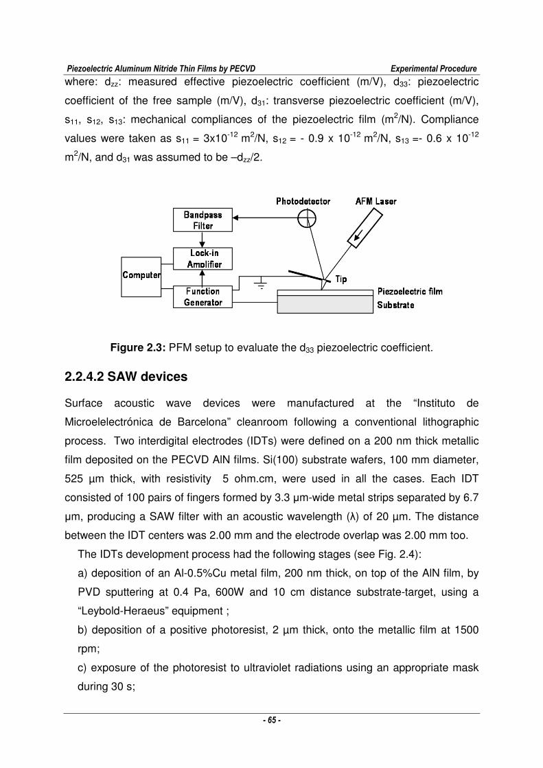
Piezoelectric Aluminum Nitride Thin Films by PECVD Experimental Procedure
- 65 -
where: dzz: measured effective piezoelectric coefficient (m/V), d33: piezoelectric
coefficient of the free sample (m/V), d31: transverse piezoelectric coefficient (m/V),
s11, s12, s13: mechanical compliances of the piezoelectric film (m2/N). Compliance
values were taken as s11 = 3x10-12 m2/N, s12 = - 0.9 x 10⁻¹² m2/N, s13 =- 0.6 x 10⁻¹²
m2/N, and d31 was assumed to be –dzz/2.
Figure 2.3: PFM setup to evaluate the d33 piezoelectric coefficient.
2.2.4.2 SAW devices
Surface acoustic wave devices were manufactured at the “Instituto de
Microelelectrónica de Barcelona” cleanroom following a conventional lithographic
process. Two interdigital electrodes (IDTs) were defined on a 200 nm thick metallic
film deposited on the PECVD AlN films. Si(100) substrate wafers, 100 mm diameter,
525 µm thick, with resistivity 5 ohm.cm, were used in all the cases. Each IDT
consisted of 100 pairs of fingers formed by 3.3 µm-wide metal strips separated by 6.7
µm, producing a SAW filter with an acoustic wavelength (λ) of 20 µm. The distance
between the IDT centers was 2.00 mm and the electrode overlap was 2.00 mm too.
The IDTs development process had the following stages (see Fig. 2.4):
a) deposition of an Al-0.5%Cu metal film, 200 nm thick, on top of the AlN film, by
PVD sputtering at 0.4 Pa, 600W and 10 cm distance substrate-target, using a
“Leybold-Heraeus” equipment ;
b) deposition of a positive photoresist, 2 µm thick, onto the metallic film at 1500
rpm;
c) exposure of the photoresist to ultraviolet radiations using an appropriate mask
during 30 s;
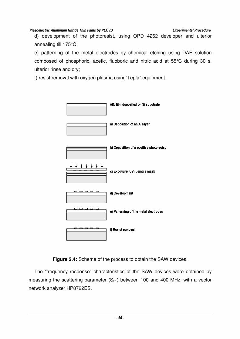
Piezoelectric Aluminum Nitride Thin Films by PECVD Experimental Procedure
- 66 -
d) development of the photoresist, using OPD 4262 developer and ulterior
annealing till 175°C;
e) patterning of the metal electrodes by chemical etching using DAE solution
composed of phosphoric, acetic, fluoboric and nitric acid at 55°C during 30 s,
ulterior rinse and dry;
f) resist removal with oxygen plasma using“Tepla” equipment.
Figure 2.4: Scheme of the process to obtain the SAW devices.
The “frequency response” characteristics of the SAW devices were obtained by
measuring the scattering parameter (S21) between 100 and 400 MHz, with a vector
network analyzer HP8722ES.
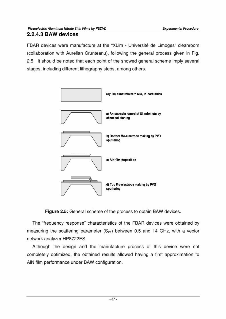
Piezoelectric Aluminum Nitride Thin Films by PECVD Experimental Procedure
- 67 -
2.2.4.3 BAW devices
FBAR devices were manufacture at the “XLim - Université de Limoges” cleanroom
(collaboration with Aurelian Crunteanu), following the general process given in Fig.
2.5. It should be noted that each point of the showed general scheme imply several
stages, including different lithography steps, among others.
Figure 2.5: General scheme of the process to obtain BAW devices.
The “frequency response” characteristics of the FBAR devices were obtained by
measuring the scattering parameter (S21) between 0.5 and 14 GHz, with a vector
network analyzer HP8722ES.
Although the design and the manufacture process of this device were not
completely optimized, the obtained results allowed having a first approximation to
AlN film performance under BAW configuration.
Piezoelectric Aluminum Nitride Thin Films by PECVD Experimental Procedure
- 68 -
2.3 Plasma characterization by Optical Emission Spectroscopy
(OES)
An experimental arrangement composed of the following elements was used:
- A Jobin Yvon THR 1000 monochromator, with 1 m focal distance, equipped with an
holographic lattice with 1200 lines / mm, and resolution power λ / ∆λ = 100 000 at
500 nm,
- A Charge Coupled Device (CCD) detector cooled with liquid nitrogen (-140ºC),
composed of a 1024 x 250 photodiodes matrix to analyzed spectral fractions at each
time,
- An UV - visible optical fiber (190-900 nm) with 0,4 mm opening.
The optical fiber was placed in the holes of the excitation guide at the top of the
reactor chamber to analyze the plasma discharge, or in the window near the bottom
of the reactor to analyze the species present near the substrate holder.
Spectra between 350 and 850 nm were obtained, with 0,36 s acquisition time, 10
repetitions, and opening from 2 to 5. Acquisition time of 10 s was used in order to
evaluate the presence of small peaks for specific intervals.
Piezoelectric Aluminum Nitride Thin Films by PECVD Growth of Polycristalline Oriented AlN Films
- 69 -
Chapter 3
GROWTH OF POLYCRYSTALLINE
ORIENTED AlN FILMS
A preliminary work had been conducted with the employed MWPECVD reactor with
its standard configuration in order to explore the viability of AlN film deposition and
the incidence of different variables on film characteristics [92]. This work had arrived
to visualize, using FTIR characterization, the reduction impurities concentration in the
film with the increase of substrate temperature. But, neither important crystalline
development nor clear preferential orientation had been detected, with XRD patterns
showing very low AlN pick intensities. However, an important development of
pulverulent deposits had been observed, which made necessary frequently reactor
cleaning in order to avoid excessive film contamination.
Consequently, those facts allowed speculating that the absence of significant
crystalline development was related with the presence of impurities in the film, being
associated to the presence of Al precursor by-products. Since the position of the
substrate holder in the reactor standard configuration was far from the plasma, with
almost a post-discharge conception, a modification in the reactor design was
introduced, allowing working with the substrate nearer the plasma. This would place
the injector and the substrate in a more energetic region, allowing a better activation
and reaction of the species [50, 63]. Since the position of the precursor injector was
fixed, a modification in the reactor design was necessary. Then, the injector could be
placed nearer the plasma, reducing the injector-plasma distance, (dip, see Fig. 2.1),
and the plasma - substrate distance (dpi + dis, see Fig. 2.1).
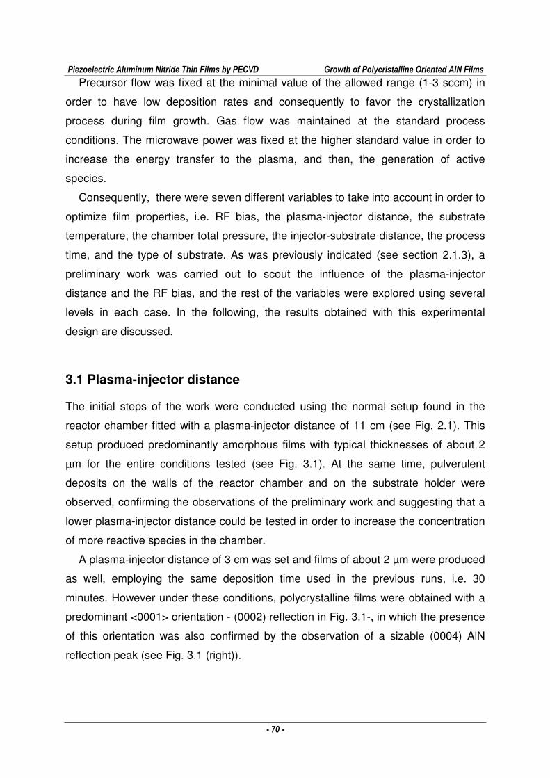
Piezoelectric Aluminum Nitride Thin Films by PECVD Growth of Polycristalline Oriented AlN Films
- 70 -
Precursor flow was fixed at the minimal value of the allowed range (1-3 sccm) in
order to have low deposition rates and consequently to favor the crystallization
process during film growth. Gas flow was maintained at the standard process
conditions. The microwave power was fixed at the higher standard value in order to
increase the energy transfer to the plasma, and then, the generation of active
species.
Consequently, there were seven different variables to take into account in order to
optimize film properties, i.e. RF bias, the plasma-injector distance, the substrate
temperature, the chamber total pressure, the injector-substrate distance, the process
time, and the type of substrate. As was previously indicated (see section 2.1.3), a
preliminary work was carried out to scout the influence of the plasma-injector
distance and the RF bias, and the rest of the variables were explored using several
levels in each case. In the following, the results obtained with this experimental
design are discussed.
3.1 Plasma-injector distance
The initial steps of the work were conducted using the normal setup found in the
reactor chamber fitted with a plasma-injector distance of 11 cm (see Fig. 2.1). This
setup produced predominantly amorphous films with typical thicknesses of about 2
µm for the entire conditions tested (see Fig. 3.1). At the same time, pulverulent
deposits on the walls of the reactor chamber and on the substrate holder were
observed, confirming the observations of the preliminary work and suggesting that a
lower plasma-injector distance could be tested in order to increase the concentration
of more reactive species in the chamber.
A plasma-injector distance of 3 cm was set and films of about 2 µm were produced
as well, employing the same deposition time used in the previous runs, i.e. 30
minutes. However under these conditions, polycrystalline films were obtained with a
predominant <0001> orientation - (0002) reflection in Fig. 3.1-, in which the presence
of this orientation was also confirmed by the observation of a sizable (0004) AlN
reflection peak (see Fig. 3.1 (right)).
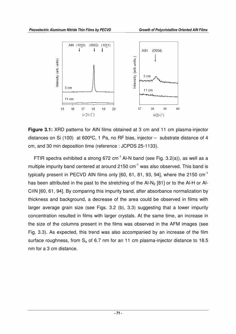
Piezoelectric Aluminum Nitride Thin Films by PECVD Growth of Polycristalline Oriented AlN Films
- 71 -
Figure 3.1: XRD patterns for AlN films obtained at 3 cm and 11 cm plasma-injector
distances on Si (100) at 600ºC, 1 Pa, no RF bias, injector – substrate distance of 4
cm, and 30 min deposition time (reference : JCPDS 25-1133).
FTIR spectra exhibited a strong 672 cm-1 Al-N band (see Fig. 3.2(a)), as well as a
multiple impurity band centered at around 2150 cm-1 was also observed. This band is
typically present in PECVD AlN films only [60, 61, 81, 93, 94], where the 2150 cm-1
has been attributed in the past to the stretching of the Al-N2 [81] or to the Al-H or Al-
C≡N [60, 61, 94]. By comparing this impurity band, after absorbance normalization by
thickness and background, a decrease of the area could be observed in films with
larger average grain size (see Figs. 3.2 (b), 3.3) suggesting that a lower impurity
concentration resulted in films with larger crystals. At the same time, an increase in
the size of the columns present in the films was observed in the AFM images (see
Fig. 3.3). As expected, this trend was also accompanied by an increase of the film
surface roughness, from Sa of 6.7 nm for an 11 cm plasma-injector distance to 18.5
nm for a 3 cm distance.
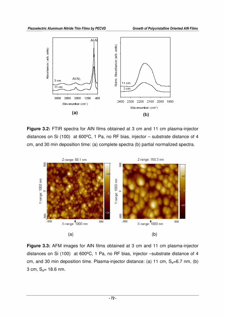
Piezoelectric Aluminum Nitride Thin Films by PECVD Growth of Polycristalline Oriented AlN Films
- 72 -
Figure 3.2: FTIR spectra for AlN films obtained at 3 cm and 11 cm plasma-injector
distances on Si (100) at 600ºC, 1 Pa, no RF bias, injector – substrate distance of 4
cm, and 30 min deposition time: (a) complete spectra (b) partial normalized spectra.
(a) (b)
Figure 3.3: AFM images for AlN films obtained at 3 cm and 11 cm plasma-injector
distances on Si (100) at 600ºC, 1 Pa, no RF bias, injector –substrate distance of 4
cm, and 30 min deposition time. Plasma-injector distance: (a) 11 cm, Sa=6.7 nm, (b)
3 cm, Sa= 18.6 nm.
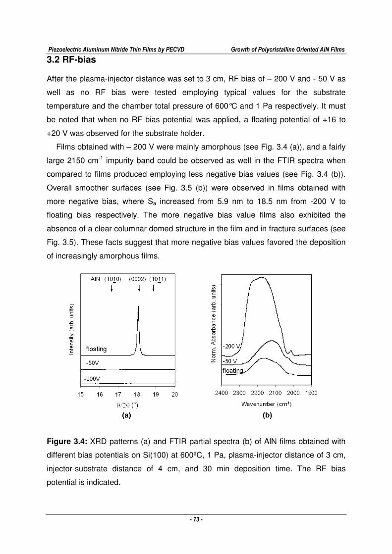
Piezoelectric Aluminum Nitride Thin Films by PECVD Growth of Polycristalline Oriented AlN Films
- 73 -
3.2 RF-bias
After the plasma-injector distance was set to 3 cm, RF bias of – 200 V and - 50 V as
well as no RF bias were tested employing typical values for the substrate
temperature and the chamber total pressure of 600°C and 1 Pa respectively. It must
be noted that when no RF bias potential was applied, a floating potential of +16 to
+20 V was observed for the substrate holder.
Films obtained with – 200 V were mainly amorphous (see Fig. 3.4 (a)), and a fairly
large 2150 cm-1 impurity band could be observed as well in the FTIR spectra when
compared to films produced employing less negative bias values (see Fig. 3.4 (b)).
Overall smoother surfaces (see Fig. 3.5 (b)) were observed in films obtained with
more negative bias, where Sa increased from 5.9 nm to 18.5 nm from -200 V to
floating bias respectively. The more negative bias value films also exhibited the
absence of a clear columnar domed structure in the film and in fracture surfaces (see
Fig. 3.5). These facts suggest that more negative bias values favored the deposition
of increasingly amorphous films.
Figure 3.4: XRD patterns (a) and FTIR partial spectra (b) of AlN films obtained with
different bias potentials on Si(100) at 600ºC, 1 Pa, plasma-injector distance of 3 cm,
injector-substrate distance of 4 cm, and 30 min deposition time. The RF bias
potential is indicated.
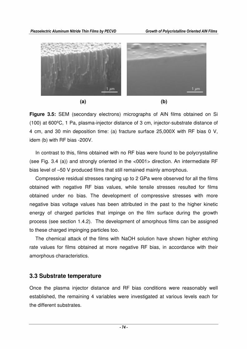
Piezoelectric Aluminum Nitride Thin Films by PECVD Growth of Polycristalline Oriented AlN Films
- 74 -
(a) (b)
Figure 3.5: SEM (secondary electrons) micrographs of AlN films obtained on Si
(100) at 600ºC, 1 Pa, plasma-injector distance of 3 cm, injector-substrate distance of
4 cm, and 30 min deposition time: (a) fracture surface 25,000X with RF bias 0 V,
idem (b) with RF bias -200V.
In contrast to this, films obtained with no RF bias were found to be polycrystalline
(see Fig. 3.4 (a)) and strongly oriented in the <0001> direction. An intermediate RF
bias level of –50 V produced films that still remained mainly amorphous.
Compressive residual stresses ranging up to 2 GPa were observed for all the films
obtained with negative RF bias values, while tensile stresses resulted for films
obtained under no bias. The development of compressive stresses with more
negative bias voltage values has been attributed in the past to the higher kinetic
energy of charged particles that impinge on the film surface during the growth
process (see section 1.4.2). The development of amorphous films can be assigned
to these charged impinging particles too.
The chemical attack of the films with NaOH solution have shown higher etching
rate values for films obtained at more negative RF bias, in accordance with their
amorphous characteristics.
3.3 Substrate temperature
Once the plasma injector distance and RF bias conditions were reasonably well
established, the remaining 4 variables were investigated at various levels each for
the different substrates.
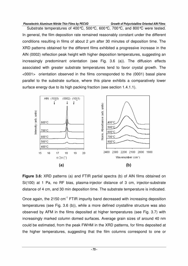
Piezoelectric Aluminum Nitride Thin Films by PECVD Growth of Polycristalline Oriented AlN Films
- 75 -
Substrate temperatures of 400°C, 500°C, 600°C, 700°C, and 800°C were tested.
In general, the film deposition rate remained reasonably constant under the different
conditions resulting in films of about 2 µm after 30 minutes of deposition time. The
XRD patterns obtained for the different films exhibited a progressive increase in the
AlN (0002) reflection peak height with higher deposition temperatures, suggesting an
increasingly predominant orientation (see Fig. 3.6 (a)). The diffusion effects
associated with greater substrate temperatures tend to favor crystal growth. The
<0001> orientation observed in the films corresponded to the (0001) basal plane
parallel to the substrate surface, where this plane exhibits a comparatively lower
surface energy due to its high packing fraction (see section 1.4.1.1).
Figure 3.6: XRD patterns (a) and FTIR partial spectra (b) of AlN films obtained on
Si(100) at 1 Pa, no RF bias, plasma-injector distance of 3 cm, injector-substrate
distance of 4 cm, and 30 min deposition time. The substrate temperature is indicated.
Once again, the 2150 cm-1 FTIR impurity band decreased with increasing deposition
temperatures (see Fig. 3.6 (b)), while a more defined crystalline structure was also
observed by AFM in the films deposited at higher temperatures (see Fig. 3.7) with
increasingly marked column domed surfaces. Average grain sizes of around 40 nm
could be estimated, from the peak FWHM in the XRD patterns, for films deposited at
the higher temperatures, suggesting that the film columns correspond to one or
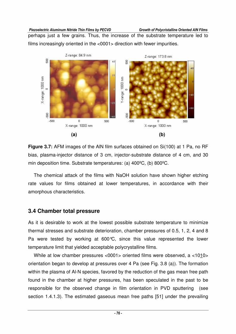
Piezoelectric Aluminum Nitride Thin Films by PECVD Growth of Polycristalline Oriented AlN Films
- 76 -
perhaps just a few grains. Thus, the increase of the substrate temperature led to
films increasingly oriented in the <0001> direction with fewer impurities.
(a) (b)
Figure 3.7: AFM images of the AlN film surfaces obtained on Si(100) at 1 Pa, no RF
bias, plasma-injector distance of 3 cm, injector-substrate distance of 4 cm, and 30
min deposition time. Substrate temperatures: (a) 400ºC, (b) 800ºC.
The chemical attack of the films with NaOH solution have shown higher etching
rate values for films obtained at lower temperatures, in accordance with their
amorphous characteristics.
3.4 Chamber total pressure
As it is desirable to work at the lowest possible substrate temperature to minimize
thermal stresses and substrate deterioration, chamber pressures of 0.5, 1, 2, 4 and 8
Pa were tested by working at 600°C, since this value represented the lower
temperature limit that yielded acceptable polycrystalline films.
While at low chamber pressures <0001> oriented films were observed, a <1010>
orientation began to develop at pressures over 4 Pa (see Fig. 3.8 (a)). The formation
within the plasma of Al-N species, favored by the reduction of the gas mean free path
found in the chamber at higher pressures, has been speculated in the past to be
responsible for the observed change in film orientation in PVD sputtering (see
section 1.4.1.3). The estimated gaseous mean free paths [51] under the prevailing
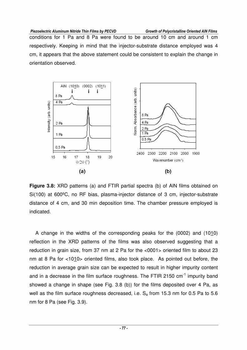
Piezoelectric Aluminum Nitride Thin Films by PECVD Growth of Polycristalline Oriented AlN Films
- 77 -
conditions for 1 Pa and 8 Pa were found to be around 10 cm and around 1 cm
respectively. Keeping in mind that the injector-substrate distance employed was 4
cm, it appears that the above statement could be consistent to explain the change in
orientation observed.
Figure 3.8: XRD patterns (a) and FTIR partial spectra (b) of AlN films obtained on
Si(100) at 600ºC, no RF bias, plasma-injector distance of 3 cm, injector-substrate
distance of 4 cm, and 30 min deposition time. The chamber pressure employed is
indicated.
A change in the widths of the corresponding peaks for the (0002) and (1010)
reflection in the XRD patterns of the films was also observed suggesting that a
reduction in grain size, from 37 nm at 2 Pa for the <0001> oriented film to about 23
nm at 8 Pa for <1010> oriented films, also took place. As pointed out before, the
reduction in average grain size can be expected to result in higher impurity content
and in a decrease in the film surface roughness. The FTIR 2150 cm-1 impurity band
showed a change in shape (see Fig. 3.8 (b)) for the films deposited over 4 Pa, as
well as the film surface roughness decreased, i.e. Sa from 15.3 nm for 0.5 Pa to 5.6
nm for 8 Pa (see Fig. 3.9).
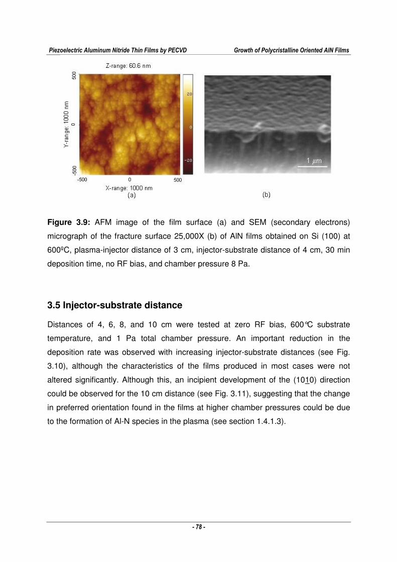
Piezoelectric Aluminum Nitride Thin Films by PECVD Growth of Polycristalline Oriented AlN Films
- 78 -
Figure 3.9: AFM image of the film surface (a) and SEM (secondary electrons)
micrograph of the fracture surface 25,000X (b) of AlN films obtained on Si (100) at
600ºC, plasma-injector distance of 3 cm, injector-substrate distance of 4 cm, 30 min
deposition time, no RF bias, and chamber pressure 8 Pa.
3.5 Injector-substrate distance
Distances of 4, 6, 8, and 10 cm were tested at zero RF bias, 600°C substrate
temperature, and 1 Pa total chamber pressure. An important reduction in the
deposition rate was observed with increasing injector-substrate distances (see Fig.
3.10), although the characteristics of the films produced in most cases were not
altered significantly. Although this, an incipient development of the (1010) direction
could be observed for the 10 cm distance (see Fig. 3.11), suggesting that the change
in preferred orientation found in the films at higher chamber pressures could be due
to the formation of Al-N species in the plasma (see section 1.4.1.3).
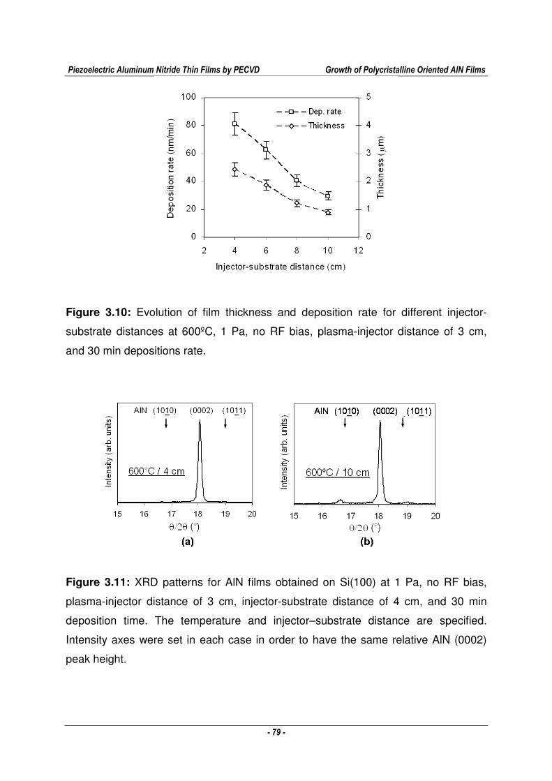
Piezoelectric Aluminum Nitride Thin Films by PECVD Growth of Polycristalline Oriented AlN Films
- 79 -
Figure 3.10: Evolution of film thickness and deposition rate for different injector-
substrate distances at 600ºC, 1 Pa, no RF bias, plasma-injector distance of 3 cm,
and 30 min depositions rate.
Figure 3.11: XRD patterns for AlN films obtained on Si(100) at 1 Pa, no RF bias,
plasma-injector distance of 3 cm, injector-substrate distance of 4 cm, and 30 min
deposition time. The temperature and injector–substrate distance are specified.
Intensity axes were set in each case in order to have the same relative AlN (0002)
peak height.
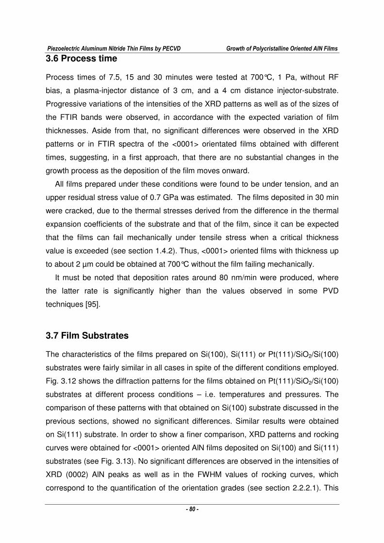
Piezoelectric Aluminum Nitride Thin Films by PECVD Growth of Polycristalline Oriented AlN Films
- 80 -
3.6 Process time
Process times of 7.5, 15 and 30 minutes were tested at 700°C, 1 Pa, without RF
bias, a plasma-injector distance of 3 cm, and a 4 cm distance injector-substrate.
Progressive variations of the intensities of the XRD patterns as well as of the sizes of
the FTIR bands were observed, in accordance with the expected variation of film
thicknesses. Aside from that, no significant differences were observed in the XRD
patterns or in FTIR spectra of the <0001> orientated films obtained with different
times, suggesting, in a first approach, that there are no substantial changes in the
growth process as the deposition of the film moves onward.
All films prepared under these conditions were found to be under tension, and an
upper residual stress value of 0.7 GPa was estimated. The films deposited in 30 min
were cracked, due to the thermal stresses derived from the difference in the thermal
expansion coefficients of the substrate and that of the film, since it can be expected
that the films can fail mechanically under tensile stress when a critical thickness
value is exceeded (see section 1.4.2). Thus, <0001> oriented films with thickness up
to about 2 µm could be obtained at 700°C without the film failing mechanically.
It must be noted that deposition rates around 80 nm/min were produced, where
the latter rate is significantly higher than the values observed in some PVD
techniques [95].
3.7 Film Substrates
The characteristics of the films prepared on Si(100), Si(111) or Pt(111)/SiO2/Si(100)
substrates were fairly similar in all cases in spite of the different conditions employed.
Fig. 3.12 shows the diffraction patterns for the films obtained on Pt(111)/SiO2/Si(100)
substrates at different process conditions – i.e. temperatures and pressures. The
comparison of these patterns with that obtained on Si(100) substrate discussed in the
previous sections, showed no significant differences. Similar results were obtained
on Si(111) substrate. In order to show a finer comparison, XRD patterns and rocking
curves were obtained for <0001> oriented AlN films deposited on Si(100) and Si(111)
substrates (see Fig. 3.13). No significant differences are observed in the intensities of
XRD (0002) AlN peaks as well as in the FWHM values of rocking curves, which
correspond to the quantification of the orientation grades (see section 2.2.2.1). This
Piezoelectric Aluminum Nitride Thin Films by PECVD Growth of Polycristalline Oriented AlN Films
- 81 -
suggests that no major epitaxial effects between the substrates used and the films
took place under the conditions tested. Pt(111) and Si(111) should induce the
<0001> orientations, in accordance with the lower mismatch between the
corresponding crystallographic plans [96]. The Si (100) surface, that could induce the
growth of a <1010> oriented AlN film, exhibited a thin interface material layer,
between the film and the substrate (see Fig. 3.14). Although the markedly low
thickness of the interface material, i.e. about 5 nm, its mere presence may upset the
epitaxial effect discussed.
Figure 3.12: XRD patterns for films deposited on Pt(111)/SiO2/Si(100) substrate with
no RF bias, plasma-injector distance of 3 cm, injector-substrate distance of 4 cm, and
30 min deposition time. The substrate temperature and chamber pressure employed
are indicated.
In order to investigate the origin of observed interface, XPS analyses were
conducted through the different stages previous to AlN film depositions (see Fig.
3.15). The original silicon surface shows the presence of silicon oxide (SiO2),
normally associated with the spontaneous oxidations of the surface. The analysis of
the substrate surface after Ar-plasma pretreatment, have evidenced the
contamination of the surface with substrate holder matter (Fe, Cr, Ni). The etching
effect produced by this treatment could act on the holder surface as well as on the
substrate, causing the ulterior deposition on the sample. Finally, the exposure of the
sample to nitrogen plasma, previous to the deposition process, has made appeared
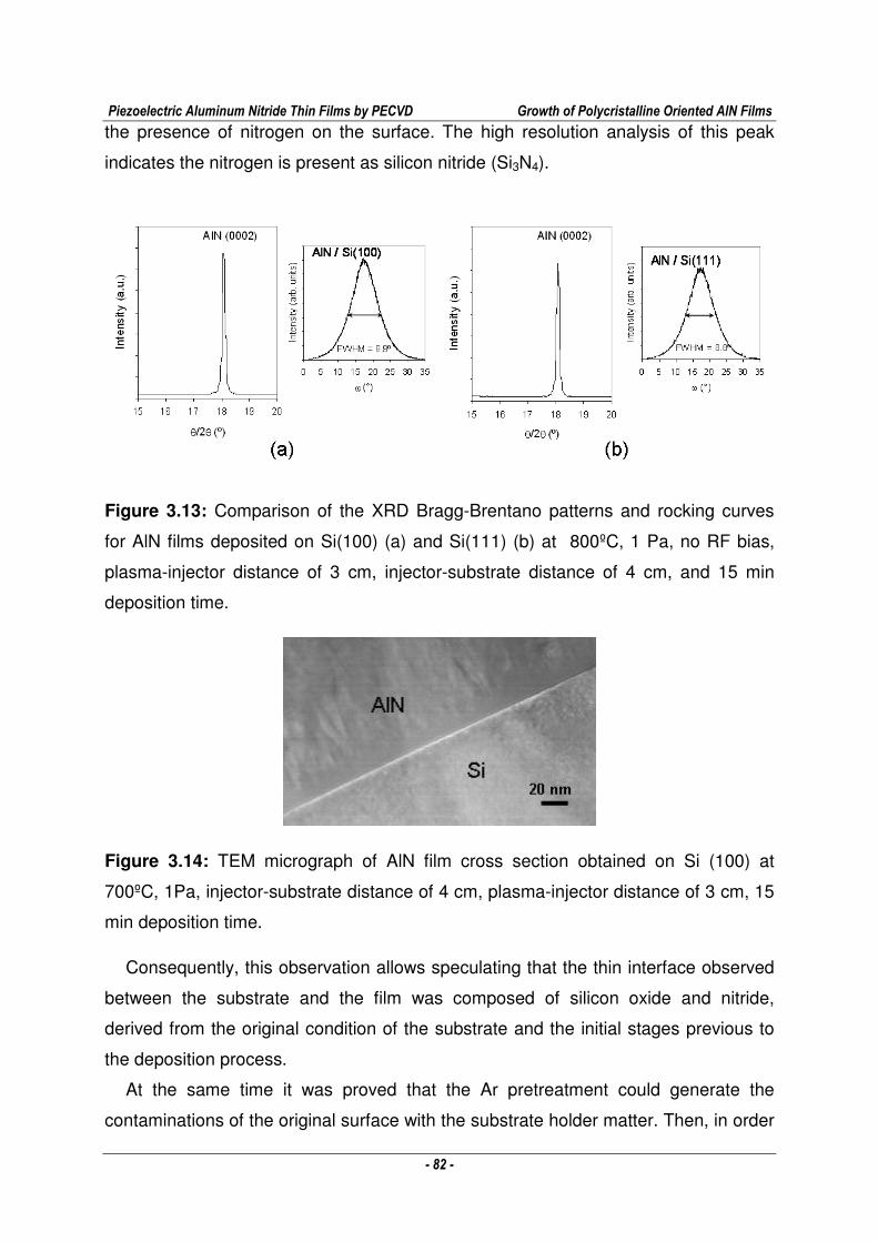
Piezoelectric Aluminum Nitride Thin Films by PECVD Growth of Polycristalline Oriented AlN Films
- 82 -
the presence of nitrogen on the surface. The high resolution analysis of this peak
indicates the nitrogen is present as silicon nitride (Si3N4).
Figure 3.13: Comparison of the XRD Bragg-Brentano patterns and rocking curves
for AlN films deposited on Si(100) (a) and Si(111) (b) at 800ºC, 1 Pa, no RF bias,
plasma-injector distance of 3 cm, injector-substrate distance of 4 cm, and 15 min
deposition time.
Figure 3.14: TEM micrograph of AlN film cross section obtained on Si (100) at
700ºC, 1Pa, injector-substrate distance of 4 cm, plasma-injector distance of 3 cm, 15
min deposition time.
Consequently, this observation allows speculating that the thin interface observed
between the substrate and the film was composed of silicon oxide and nitride,
derived from the original condition of the substrate and the initial stages previous to
the deposition process.
At the same time it was proved that the Ar pretreatment could generate the
contaminations of the original surface with the substrate holder matter. Then, in order
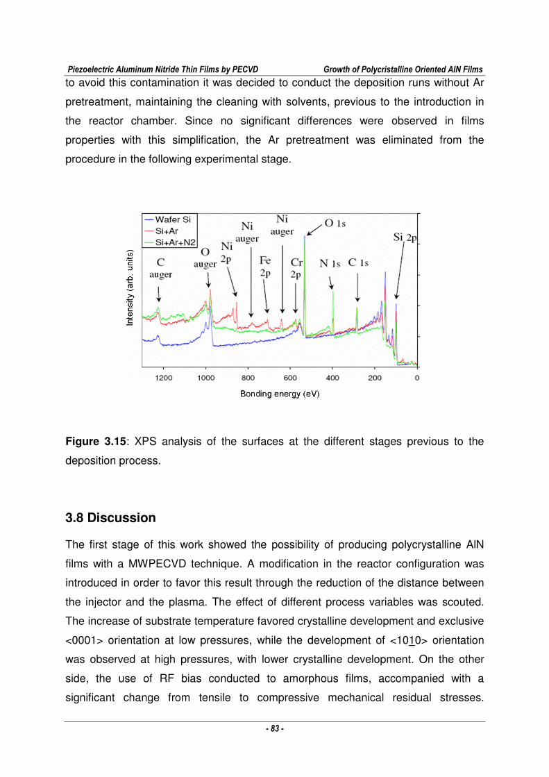
Piezoelectric Aluminum Nitride Thin Films by PECVD Growth of Polycristalline Oriented AlN Films
- 83 -
to avoid this contamination it was decided to conduct the deposition runs without Ar
pretreatment, maintaining the cleaning with solvents, previous to the introduction in
the reactor chamber. Since no significant differences were observed in films
properties with this simplification, the Ar pretreatment was eliminated from the
procedure in the following experimental stage.
Figure 3.15: XPS analysis of the surfaces at the different stages previous to the
deposition process.
3.8 Discussion
The first stage of this work showed the possibility of producing polycrystalline AlN
films with a MWPECVD technique. A modification in the reactor configuration was
introduced in order to favor this result through the reduction of the distance between
the injector and the plasma. The effect of different process variables was scouted.
The increase of substrate temperature favored crystalline development and exclusive
<0001> orientation at low pressures, while the development of <1010> orientation
was observed at high pressures, with lower crystalline development. On the other
side, the use of RF bias conducted to amorphous films, accompanied with a
significant change from tensile to compressive mechanical residual stresses.
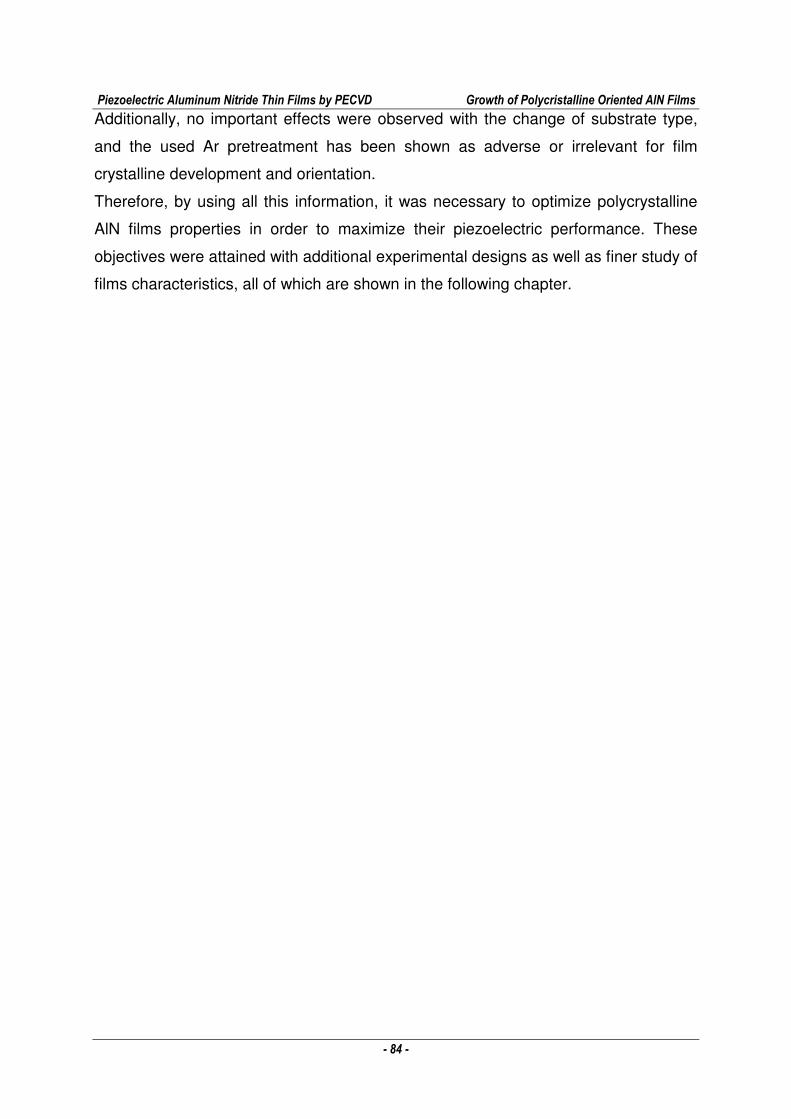
Piezoelectric Aluminum Nitride Thin Films by PECVD Growth of Polycristalline Oriented AlN Films
- 84 -
Additionally, no important effects were observed with the change of substrate type,
and the used Ar pretreatment has been shown as adverse or irrelevant for film
crystalline development and orientation.
Therefore, by using all this information, it was necessary to optimize polycrystalline
AlN films properties in order to maximize their piezoelectric performance. These
objectives were attained with additional experimental designs as well as finer study of
films characteristics, all of which are shown in the following chapter.
Piezoelectric Aluminum Nitride Thin Films by PECVD Optimization of Film Properties
- 85 -
Chapter 4
OPTMIZATION OF FILM PROPERTIES
In the first part of this work it was demonstrated that polycrystalline AlN films are
possible to be produced by MWPECVD technique and the film preferential orientation
is possible to be controlled as <0001> or <1010> by adequate selection of the
deposition conditions. In order to optimize the properties of the AlN films for electro-
acoustic applications, additional experiences were conducted. A full fledged
experimental design for substrate temperature and total pressure in three levels was
done in order to optimize the development of <1010> oriented films. Film thickness
and bias potential were explored separately using several new levels in each case in
order to optimize the properties of <0001> oriented films. A finer characterization of
the microstructure, as well as the measurement of the piezoelectric performance of
the films was introduced in this stage. Plasma diagnostic by OES in optimal process
conditions complete this chapter.
As a consequence of the results obtained in the previous chapter, the runs at this
stage were conducted without Ar pretreatment. Moreover, films were prepared mainly
with thicknesses lower than 1 µm in order to avoid cracking and at the same time to
make a finer analysis of the FTIR transmission spectra.
4.1 Pressure-temperature combined effect
According to previous observations, temperature and pressure are important
variables in order to reach crystalline development and change the preferential
orientation. Then a complete study of the effect of both variables was considered
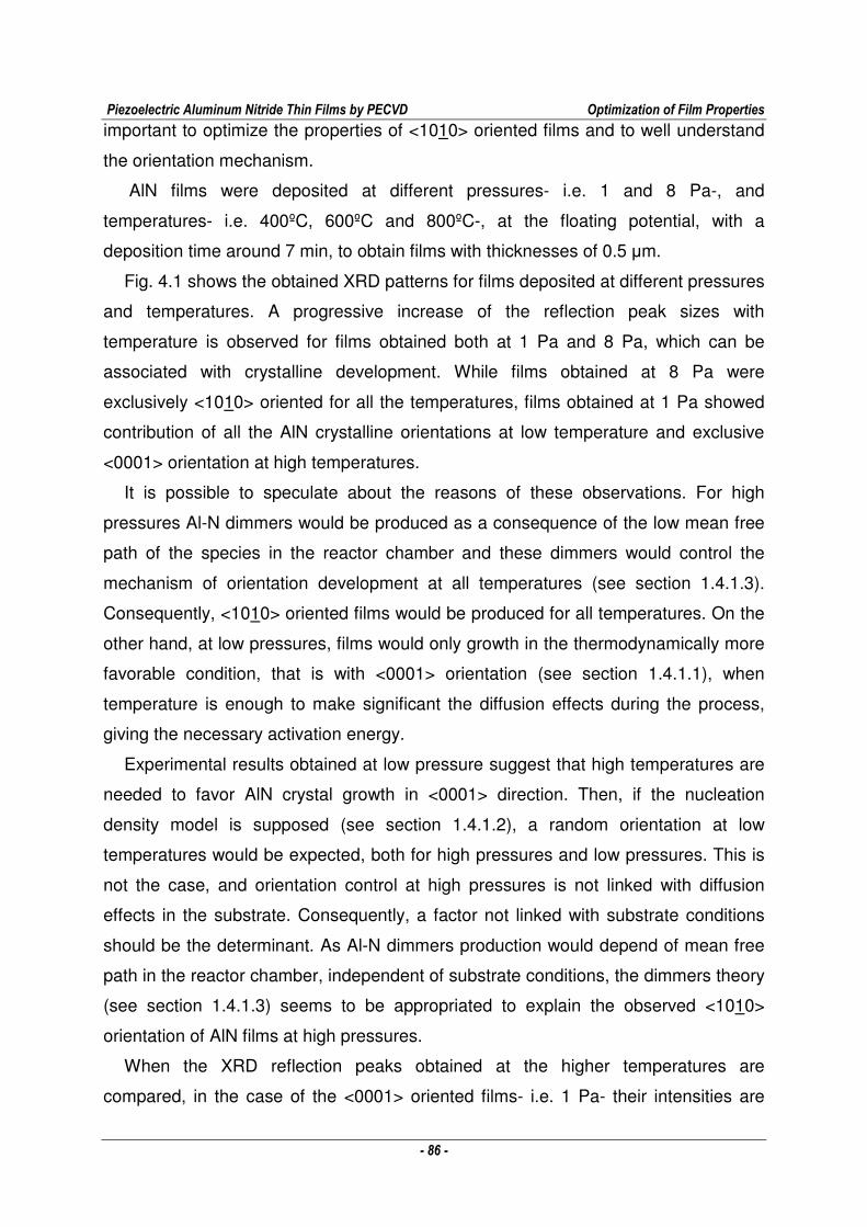
Piezoelectric Aluminum Nitride Thin Films by PECVD Optimization of Film Properties
- 86 -
important to optimize the properties of <1010> oriented films and to well understand
the orientation mechanism.
AlN films were deposited at different pressures- i.e. 1 and 8 Pa-, and
temperatures- i.e. 400ºC, 600ºC and 800ºC-, at the floating potential, with a
deposition time around 7 min, to obtain films with thicknesses of 0.5 µm.
Fig. 4.1 shows the obtained XRD patterns for films deposited at different pressures
and temperatures. A progressive increase of the reflection peak sizes with
temperature is observed for films obtained both at 1 Pa and 8 Pa, which can be
associated with crystalline development. While films obtained at 8 Pa were
exclusively <1010> oriented for all the temperatures, films obtained at 1 Pa showed
contribution of all the AlN crystalline orientations at low temperature and exclusive
<0001> orientation at high temperatures.
It is possible to speculate about the reasons of these observations. For high
pressures Al-N dimmers would be produced as a consequence of the low mean free
path of the species in the reactor chamber and these dimmers would control the
mechanism of orientation development at all temperatures (see section 1.4.1.3).
Consequently, <1010> oriented films would be produced for all temperatures. On the
other hand, at low pressures, films would only growth in the thermodynamically more
favorable condition, that is with <0001> orientation (see section 1.4.1.1), when
temperature is enough to make significant the diffusion effects during the process,
giving the necessary activation energy.
Experimental results obtained at low pressure suggest that high temperatures are
needed to favor AlN crystal growth in <0001> direction. Then, if the nucleation
density model is supposed (see section 1.4.1.2), a random orientation at low
temperatures would be expected, both for high pressures and low pressures. This is
not the case, and orientation control at high pressures is not linked with diffusion
effects in the substrate. Consequently, a factor not linked with substrate conditions
should be the determinant. As Al-N dimmers production would depend of mean free
path in the reactor chamber, independent of substrate conditions, the dimmers theory
(see section 1.4.1.3) seems to be appropriated to explain the observed <1010>
orientation of AlN films at high pressures.
When the XRD reflection peaks obtained at the higher temperatures are
compared, in the case of the <0001> oriented films- i.e. 1 Pa- their intensities are
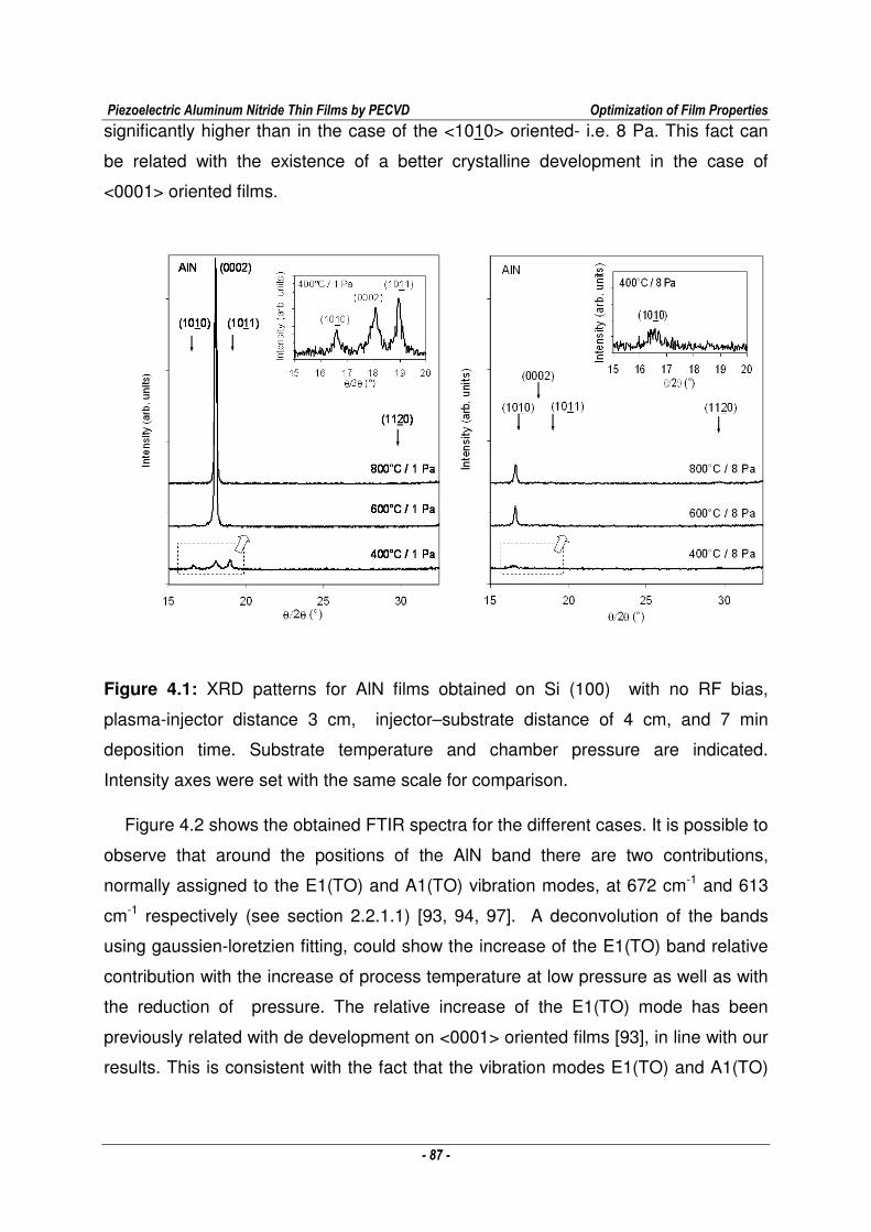
Piezoelectric Aluminum Nitride Thin Films by PECVD Optimization of Film Properties
- 87 -
significantly higher than in the case of the <1010> oriented- i.e. 8 Pa. This fact can
be related with the existence of a better crystalline development in the case of
<0001> oriented films.
Figure 4.1: XRD patterns for AlN films obtained on Si (100) with no RF bias,
plasma-injector distance 3 cm, injector–substrate distance of 4 cm, and 7 min
deposition time. Substrate temperature and chamber pressure are indicated.
Intensity axes were set with the same scale for comparison.
Figure 4.2 shows the obtained FTIR spectra for the different cases. It is possible to
observe that around the positions of the AlN band there are two contributions,
normally assigned to the E1(TO) and A1(TO) vibration modes, at 672 cm-1 and 613
cm-1 respectively (see section 2.2.1.1) [93, 94, 97]. A deconvolution of the bands
using gaussien-loretzien fitting, could show the increase of the E1(TO) band relative
contribution with the increase of process temperature at low pressure as well as with
the reduction of pressure. The relative increase of the E1(TO) mode has been
previously related with de development on <0001> oriented films [93], in line with our
results. This is consistent with the fact that the vibration modes E1(TO) and A1(TO)
Piezoelectric Aluminum Nitride Thin Films by PECVD Optimization of Film Properties
- 88 -
correspond respectively to modes excited by a perpendicular and parallel electric
field to the c-axis of the crystallite [98].
Figure 4.2: Partial FTIR transmission spectra for AlN films obtained on Si (100) with
no RF bias, plasma-injector distance of 3 cm, injector–substrate distance of 4 cm,
and thicknesses of 0.5 µm. Substrate temperature and chamber pressure are
indicated. Absorbance axes of different wavenumber ranges were set with the same
scale for comparison.
Piezoelectric Aluminum Nitride Thin Films by PECVD Optimization of Film Properties
- 89 -
In addition, a significant decrease of the 2150 cm-1 impurity band with temperature
increase has been observed for both pressures (see Fig. 4.2). This 2150 cm-1 band,
has been traditionally assigned to different impurities- e.g. CN, Al-H- as was
previously discussed (section 3.1). Simultaneously, the analysis of the plasma during
the deposition process by Optical Emission Spectroscopy (OES) (see section 4.6)
evidenced the presence of CN species in the reactor chamber. This species could
result from the reaction between nitrogen and the Al-precursor (TMA) and could be
incorporated as impurities in the film structure during its growth [61].
It can be speculated that at low process temperatures the impurities associated to
the decomposition of TMA are incorporated in the film because they arrived to the
surface, but probably they can not diffuse and desorbed from it [27]. Together, the
low surface diffusion of AlN species does not allow a good crystal growth. However,
at higher temperatures, the surface diffusion during the film growth allowed for a
crystalline development.
Therefore, higher temperatures have allowed to improve the film crystalline
development both for <0001> and <1010> oriented films. At the same time, <0001>
oriented films reached a better crystalline development than the <1010> oriented
films.
4.1.1 Annealing effect
In order to better understand temperature effect on the microstructure, AlN films
obtained at 400°C and 1 Pa were post-treated by annealing at 800°C for 2 hours
under vacuum. The comparison between XRD pattern of the samples before and
after annealing (see Fig. 4.3) showed no improvement of film crystallization and
preferential orientation since there were not significant changes in size and relative
contribution of the (0002) reflection peaks. Conversely, XRD pattern of films
obtained at 800ºC had shown marked crystalline development and preferential
orientation (see Fig. 4.3). These differences suggest that thermal effect was
determinant during film growth but had minor contribution after it. According to that
previously discussed, high temperatures during film growth (800ºC) allowed surface
diffusion of the arriving species and desorption of impurities associated with the
precursor decomposition, all favorable for a better crystalline development.
Simultaneously, <0001> orientation was favored by the minimization of surface
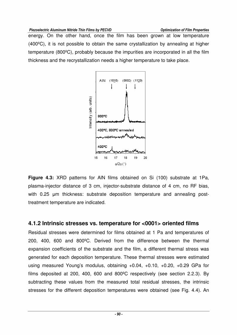
Piezoelectric Aluminum Nitride Thin Films by PECVD Optimization of Film Properties
- 90 -
energy. On the other hand, once the film has been grown at low temperature
(400ºC), it is not possible to obtain the same crystallization by annealing at higher
temperature (800ºC), probably because the impurities are incorporated in all the film
thickness and the recrystallization needs a higher temperature to take place.
Figure 4.3: XRD patterns for AlN films obtained on Si (100) substrate at 1Pa,
plasma-injector distance of 3 cm, injector-substrate distance of 4 cm, no RF bias,
with 0.25 µm thickness: substrate deposition temperature and annealing post-
treatment temperature are indicated.
4.1.2 Intrinsic stresses vs. temperature for <0001> oriented films
Residual stresses were determined for films obtained at 1 Pa and temperatures of
200, 400, 600 and 800ºC. Derived from the difference between the thermal
expansion coefficients of the substrate and the film, a different thermal stress was
generated for each deposition temperature. These thermal stresses were estimated
using measured Young’s modulus, obtaining +0.04, +0.10, +0.20, +0.29 GPa for
films deposited at 200, 400, 600 and 800ºC respectively (see section 2.2.3). By
subtracting these values from the measured total residual stresses, the intrinsic
stresses for the different deposition temperatures were obtained (see Fig. 4.4). An
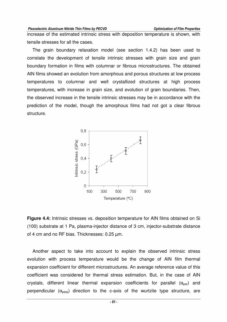
Piezoelectric Aluminum Nitride Thin Films by PECVD Optimization of Film Properties
- 91 -
increase of the estimated intrinsic stress with deposition temperature is shown, with
tensile stresses for all the cases.
The grain boundary relaxation model (see section 1.4.2) has been used to
correlate the development of tensile intrinsic stresses with grain size and grain
boundary formation in films with columnar or fibrous microstructures. The obtained
AlN films showed an evolution from amorphous and porous structures at low process
temperatures to columnar and well crystallized structures at high process
temperatures, with increase in grain size, and evolution of grain boundaries. Then,
the observed increase in the tensile intrinsic stresses may be in accordance with the
prediction of the model, though the amorphous films had not got a clear fibrous
structure.
Figure 4.4: Intrinsic stresses vs. deposition temperature for AlN films obtained on Si
(100) substrate at 1 Pa, plasma-injector distance of 3 cm, injector-substrate distance
of 4 cm and no RF bias. Thicknesses: 0.25 µm.
Another aspect to take into account to explain the observed intrinsic stress
evolution with process temperature would be the change of AlN film thermal
expansion coefficient for different microstructures. An average reference value of this
coefficient was considered for thermal stress estimation. But, in the case of AlN
crystals, different linear thermal expansion coefficients for parallel (αpar) and
perpendicular (αperp) direction to the c-axis of the wurtzite type structure, are
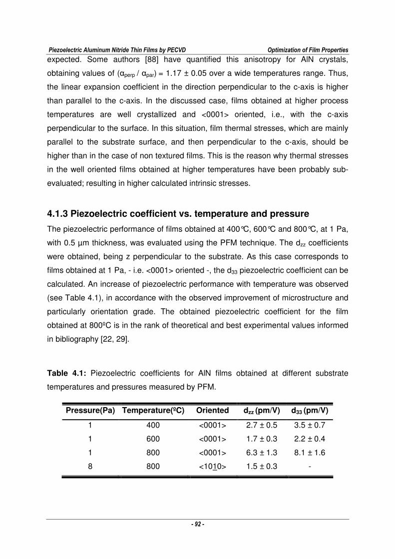
Piezoelectric Aluminum Nitride Thin Films by PECVD Optimization of Film Properties
- 92 -
expected. Some authors [88] have quantified this anisotropy for AlN crystals,
obtaining values of (αperp / αpar) = 1.17 ± 0.05 over a wide temperatures range. Thus,
the linear expansion coefficient in the direction perpendicular to the c-axis is higher
than parallel to the c-axis. In the discussed case, films obtained at higher process
temperatures are well crystallized and <0001> oriented, i.e., with the c-axis
perpendicular to the surface. In this situation, film thermal stresses, which are mainly
parallel to the substrate surface, and then perpendicular to the c-axis, should be
higher than in the case of non textured films. This is the reason why thermal stresses
in the well oriented films obtained at higher temperatures have been probably sub-
evaluated; resulting in higher calculated intrinsic stresses.
4.1.3 Piezoelectric coefficient vs. temperature and pressure
The piezoelectric performance of films obtained at 400°C, 600°C and 800°C, at 1 Pa,
with 0.5 µm thickness, was evaluated using the PFM technique. The dzz coefficients
were obtained, being z perpendicular to the substrate. As this case corresponds to
films obtained at 1 Pa, - i.e. <0001> oriented -, the d33 piezoelectric coefficient can be
calculated. An increase of piezoelectric performance with temperature was observed
(see Table 4.1), in accordance with the observed improvement of microstructure and
particularly orientation grade. The obtained piezoelectric coefficient for the film
obtained at 800ºC is in the rank of theoretical and best experimental values informed
in bibliography [22, 29].
Table 4.1: Piezoelectric coefficients for AlN films obtained at different substrate
temperatures and pressures measured by PFM.
Pressure(Pa) Temperature(ºC) Oriented dzz (pm/V) d33 (pm/V)
1 400 <0001> 2.7 ± 0.5 3.5 ± 0.7
1 600 <0001> 1.7 ± 0.3 2.2 ± 0.4
1 800 <0001> 6.3 ± 1.3 8.1 ± 1.6
8 800 <1010> 1.5 ± 0.3 -
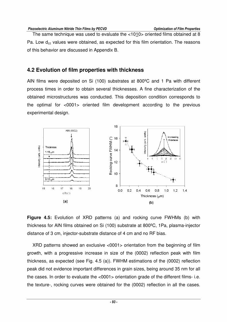
Piezoelectric Aluminum Nitride Thin Films by PECVD Optimization of Film Properties
- 93 -
The same technique was used to evaluate the <1010> oriented films obtained at 8
Pa. Low dzz values were obtained, as expected for this film orientation. The reasons
of this behavior are discussed in Appendix B.
4.2 Evolution of film properties with thickness
AlN films were deposited on Si (100) substrates at 800ºC and 1 Pa with different
process times in order to obtain several thicknesses. A fine characterization of the
obtained microstructures was conducted. This deposition condition corresponds to
the optimal for <0001> oriented film development according to the previous
experimental design.
Figure 4.5: Evolution of XRD patterns (a) and rocking curve FWHMs (b) with
thickness for AlN films obtained on Si (100) substrate at 800ºC, 1Pa, plasma-injector
distance of 3 cm, injector-substrate distance of 4 cm and no RF bias.
XRD patterns showed an exclusive <0001> orientation from the beginning of film
growth, with a progressive increase in size of the (0002) reflection peak with film
thickness, as expected (see Fig. 4.5 (a)). FWHM estimations of the (0002) reflection
peak did not evidence important differences in grain sizes, being around 35 nm for all
the cases. In order to evaluate the <0001> orientation grade of the different films- i.e.
the texture-, rocking curves were obtained for the (0002) reflection in all the cases.
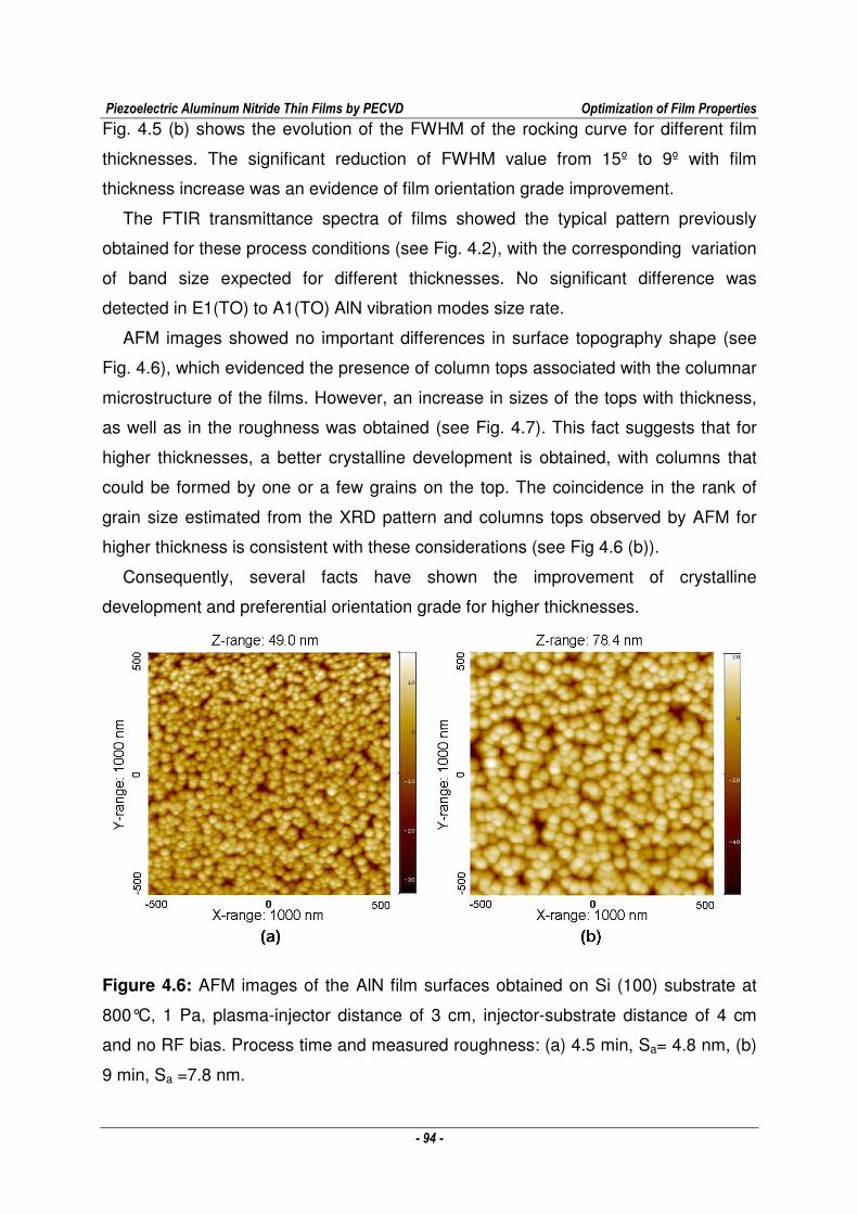
Piezoelectric Aluminum Nitride Thin Films by PECVD Optimization of Film Properties
- 94 -
Fig. 4.5 (b) shows the evolution of the FWHM of the rocking curve for different film
thicknesses. The significant reduction of FWHM value from 15º to 9º with film
thickness increase was an evidence of film orientation grade improvement.
The FTIR transmittance spectra of films showed the typical pattern previously
obtained for these process conditions (see Fig. 4.2), with the corresponding variation
of band size expected for different thicknesses. No significant difference was
detected in E1(TO) to A1(TO) AlN vibration modes size rate.
AFM images showed no important differences in surface topography shape (see
Fig. 4.6), which evidenced the presence of column tops associated with the columnar
microstructure of the films. However, an increase in sizes of the tops with thickness,
as well as in the roughness was obtained (see Fig. 4.7). This fact suggests that for
higher thicknesses, a better crystalline development is obtained, with columns that
could be formed by one or a few grains on the top. The coincidence in the rank of
grain size estimated from the XRD pattern and columns tops observed by AFM for
higher thickness is consistent with these considerations (see Fig 4.6 (b)).
Consequently, several facts have shown the improvement of crystalline
development and preferential orientation grade for higher thicknesses.
Figure 4.6: AFM images of the AlN film surfaces obtained on Si (100) substrate at
800°C, 1 Pa, plasma-injector distance of 3 cm, injector-substrate distance of 4 cm
and no RF bias. Process time and measured roughness: (a) 4.5 min, Sa= 4.8 nm, (b)
9 min, Sa =7.8 nm.
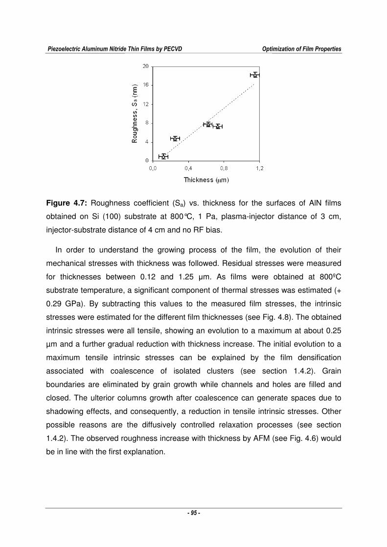
Piezoelectric Aluminum Nitride Thin Films by PECVD Optimization of Film Properties
- 95 -
Figure 4.7: Roughness coefficient (Sa) vs. thickness for the surfaces of AlN films
obtained on Si (100) substrate at 800°C, 1 Pa, plasma-injector distance of 3 cm,
injector-substrate distance of 4 cm and no RF bias.
In order to understand the growing process of the film, the evolution of their
mechanical stresses with thickness was followed. Residual stresses were measured
for thicknesses between 0.12 and 1.25 µm. As films were obtained at 800ºC
substrate temperature, a significant component of thermal stresses was estimated (+
0.29 GPa). By subtracting this values to the measured film stresses, the intrinsic
stresses were estimated for the different film thicknesses (see Fig. 4.8). The obtained
intrinsic stresses were all tensile, showing an evolution to a maximum at about 0.25
µm and a further gradual reduction with thickness increase. The initial evolution to a
maximum tensile intrinsic stresses can be explained by the film densification
associated with coalescence of isolated clusters (see section 1.4.2). Grain
boundaries are eliminated by grain growth while channels and holes are filled and
closed. The ulterior columns growth after coalescence can generate spaces due to
shadowing effects, and consequently, a reduction in tensile intrinsic stresses. Other
possible reasons are the diffusively controlled relaxation processes (see section
1.4.2). The observed roughness increase with thickness by AFM (see Fig. 4.6) would
be in line with the first explanation.
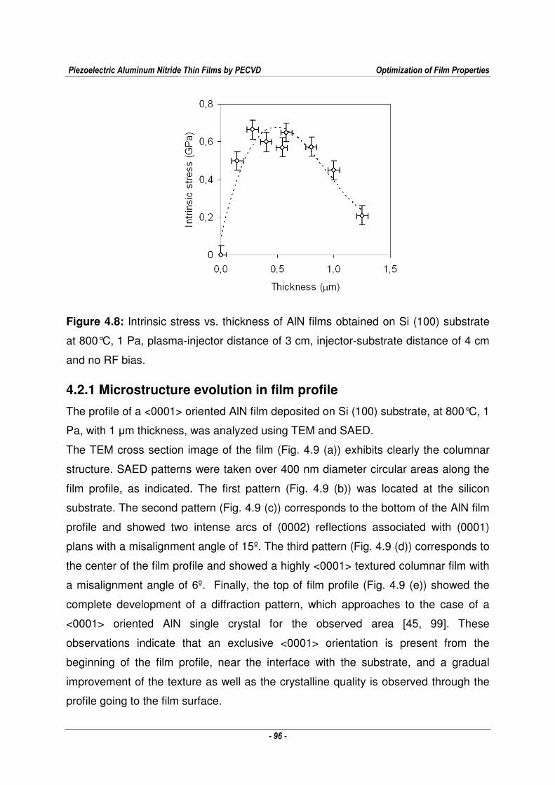
Piezoelectric Aluminum Nitride Thin Films by PECVD Optimization of Film Properties
- 96 -
Figure 4.8: Intrinsic stress vs. thickness of AlN films obtained on Si (100) substrate
at 800°C, 1 Pa, plasma-injector distance of 3 cm, injector-substrate distance of 4 cm
and no RF bias.
4.2.1 Microstructure evolution in film profile
The profile of a <0001> oriented AlN film deposited on Si (100) substrate, at 800°C, 1
Pa, with 1 µm thickness, was analyzed using TEM and SAED.
The TEM cross section image of the film (Fig. 4.9 (a)) exhibits clearly the columnar
structure. SAED patterns were taken over 400 nm diameter circular areas along the
film profile, as indicated. The first pattern (Fig. 4.9 (b)) was located at the silicon
substrate. The second pattern (Fig. 4.9 (c)) corresponds to the bottom of the AlN film
profile and showed two intense arcs of (0002) reflections associated with (0001)
plans with a misalignment angle of 15º. The third pattern (Fig. 4.9 (d)) corresponds to
the center of the film profile and showed a highly <0001> textured columnar film with
a misalignment angle of 6º. Finally, the top of film profile (Fig. 4.9 (e)) showed the
complete development of a diffraction pattern, which approaches to the case of a
<0001> oriented AlN single crystal for the observed area [45, 99]. These
observations indicate that an exclusive <0001> orientation is present from the
beginning of the film profile, near the interface with the substrate, and a gradual
improvement of the texture as well as the crystalline quality is observed through the
profile going to the film surface.
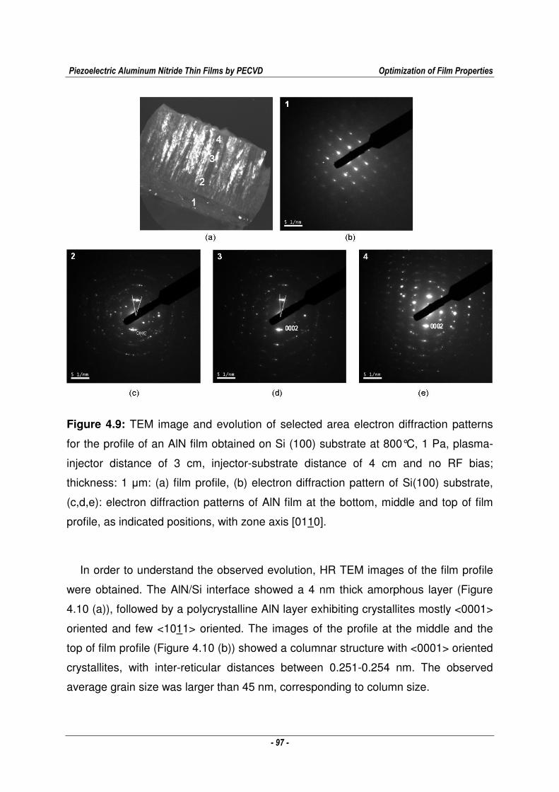
Piezoelectric Aluminum Nitride Thin Films by PECVD Optimization of Film Properties
- 97 -
Figure 4.9: TEM image and evolution of selected area electron diffraction patterns
for the profile of an AlN film obtained on Si (100) substrate at 800°C, 1 Pa, plasma-
injector distance of 3 cm, injector-substrate distance of 4 cm and no RF bias;
thickness: 1 µm: (a) film profile, (b) electron diffraction pattern of Si(100) substrate,
(c,d,e): electron diffraction patterns of AlN film at the bottom, middle and top of film
profile, as indicated positions, with zone axis [0110].
In order to understand the observed evolution, HR TEM images of the film profile
were obtained. The AlN/Si interface showed a 4 nm thick amorphous layer (Figure
4.10 (a)), followed by a polycrystalline AlN layer exhibiting crystallites mostly <0001>
oriented and few <1011> oriented. The images of the profile at the middle and the
top of film profile (Figure 4.10 (b)) showed a columnar structure with <0001> oriented
crystallites, with inter-reticular distances between 0.251-0.254 nm. The observed
average grain size was larger than 45 nm, corresponding to column size.
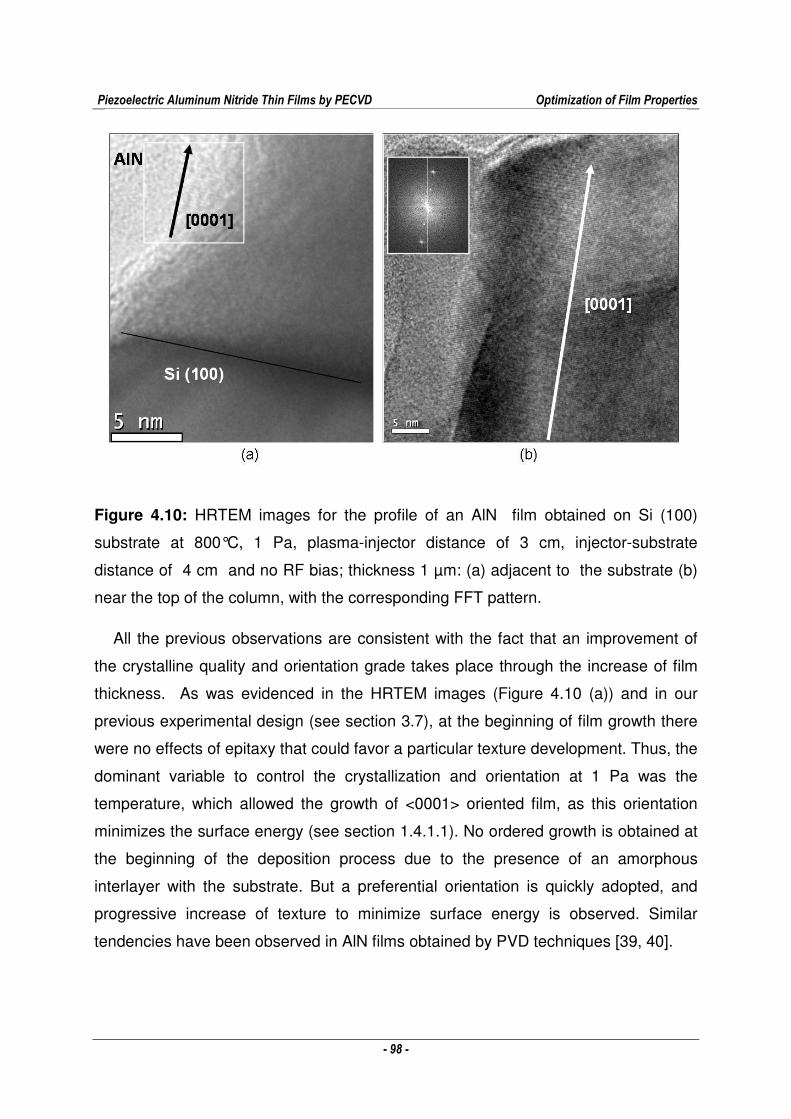
Piezoelectric Aluminum Nitride Thin Films by PECVD Optimization of Film Properties
- 98 -
Figure 4.10: HRTEM images for the profile of an AlN film obtained on Si (100)
substrate at 800°C, 1 Pa, plasma-injector distance of 3 cm, injector-substrate
distance of 4 cm and no RF bias; thickness 1 µm: (a) adjacent to the substrate (b)
near the top of the column, with the corresponding FFT pattern.
All the previous observations are consistent with the fact that an improvement of
the crystalline quality and orientation grade takes place through the increase of film
thickness. As was evidenced in the HRTEM images (Figure 4.10 (a)) and in our
previous experimental design (see section 3.7), at the beginning of film growth there
were no effects of epitaxy that could favor a particular texture development. Thus, the
dominant variable to control the crystallization and orientation at 1 Pa was the
temperature, which allowed the growth of <0001> oriented film, as this orientation
minimizes the surface energy (see section 1.4.1.1). No ordered growth is obtained at
the beginning of the deposition process due to the presence of an amorphous
interlayer with the substrate. But a preferential orientation is quickly adopted, and
progressive increase of texture to minimize surface energy is observed. Similar
tendencies have been observed in AlN films obtained by PVD techniques [39, 40].
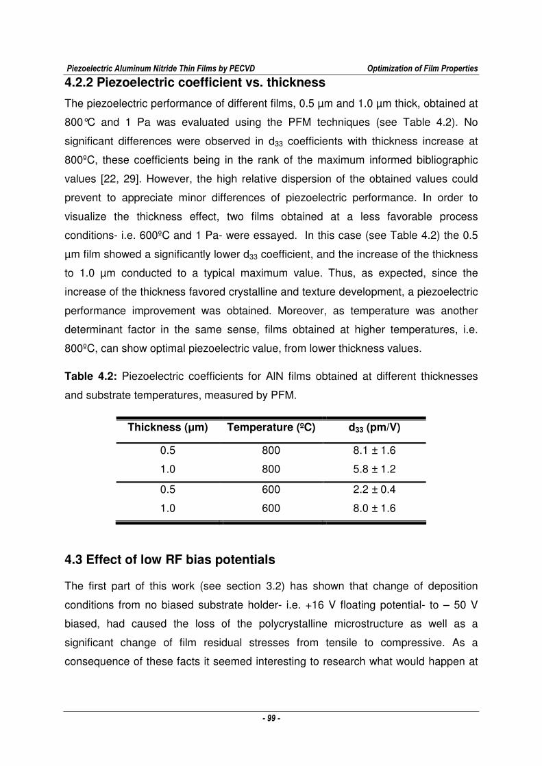
Piezoelectric Aluminum Nitride Thin Films by PECVD Optimization of Film Properties
- 99 -
4.2.2 Piezoelectric coefficient vs. thickness
The piezoelectric performance of different films, 0.5 µm and 1.0 µm thick, obtained at
800°C and 1 Pa was evaluated using the PFM techniques (see Table 4.2). No
significant differences were observed in d33 coefficients with thickness increase at
800ºC, these coefficients being in the rank of the maximum informed bibliographic
values [22, 29]. However, the high relative dispersion of the obtained values could
prevent to appreciate minor differences of piezoelectric performance. In order to
visualize the thickness effect, two films obtained at a less favorable process
conditions- i.e. 600ºC and 1 Pa- were essayed. In this case (see Table 4.2) the 0.5
µm film showed a significantly lower d33 coefficient, and the increase of the thickness
to 1.0 µm conducted to a typical maximum value. Thus, as expected, since the
increase of the thickness favored crystalline and texture development, a piezoelectric
performance improvement was obtained. Moreover, as temperature was another
determinant factor in the same sense, films obtained at higher temperatures, i.e.
800ºC, can show optimal piezoelectric value, from lower thickness values.
Table 4.2: Piezoelectric coefficients for AlN films obtained at different thicknesses
and substrate temperatures, measured by PFM.
Thickness (µm) Temperature (ºC) d33 (pm/V)
0.5 800 8.1 ± 1.6
1.0 800 5.8 ± 1.2
0.5 600 2.2 ± 0.4
1.0 600 8.0 ± 1.6
4.3 Effect of low RF bias potentials
The first part of this work (see section 3.2) has shown that change of deposition
conditions from no biased substrate holder- i.e. +16 V floating potential- to – 50 V
biased, had caused the loss of the polycrystalline microstructure as well as a
significant change of film residual stresses from tensile to compressive. As a
consequence of these facts it seemed interesting to research what would happen at
Piezoelectric Aluminum Nitride Thin Films by PECVD Optimization of Film Properties
- 100 -
intermediate bias values in order to optimize process conditions in the following
direction:
- maximizing crystalline development, whose condition could be obtained at low bias
potential values;
- minimizing film residual stresses by maintaining adequate crystalline development,
as desired for electroacoustic devices;
- maximizing film thickness- without cracks- in order to improve microstructure and
piezoelectric performance. The improvement of films microstructure with thickness
was previously shown working with no bias potentials, but there was a maximum
thickness for which films were possible to be produced without cracks. If residual
tensile stresses are possible to be reduced with low bias potentials probably higher
thickness could be attained without cracks. Then, if the observed tendency in
microstructure evolution with thickness is maintained at low bias potentials, the
microstructure and piezoelectric performance could be improved.
AlN films were deposited at different bias potentials, from the floating potential
(+16V) to -40V, at 800ºC and 1 Pa, with a deposition time of 7 min, which allowed
obtaining film thickness of 0.5 µm.
Figure 4.11 shows the XRD patterns obtained in different cases. An exclusive
<0001> orientation was observed in the case of no biased substrate holder, i.e. at
floating potential, as would be expected according to the previous work. Once the
substrate holder began to be biased, the intensity of the (0002) reflection peak began
to decrease progressively in the direction of negative bias potentials. At the same
time, the FWHM of the reflection peak increased, associated with a grain size
decrease. These facts can be linked with a progressive decrease in film crystalline
development, in accordance with our previous results showing amorphous films for
higher bias potentials (see section 3.2). Simultaneously, a significant displacement in
the position of the (0002) reflection peak from +16V to -20V bias potentials can be
observed. This effect can be assigned to the increase in spacing between (0001)
plans of the lattice due to the change in film residual stresses. If a polycrystalline film,
containing an isotropic biaxial tensile stress distribution in the xy plane (parallel to the
substrate) and no stresses in the z direction (σz = 0), is assumed, the film contracts in
the z direction (perpendicular to the substrate) by an amount given by [58]:
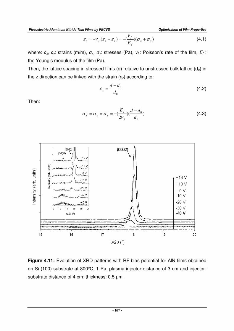
Piezoelectric Aluminum Nitride Thin Films by PECVD Optimization of Film Properties
- 101 -
))(()( yx
f
f
yxfzE
σσν
εενε +−=+−= (4.1)
where: єx, єy: strains (m/m), σx, σy: stresses (Pa), νf : Poisson’s rate of the film, Ef :
the Young’s modulus of the film (Pa).
Then, the lattice spacing in stressed films (d) relative to unstressed bulk lattice (d0) in
the z direction can be linked with the strain (єz) according to:
0
0
d
ddz
−=ε (4.2)
Then:
))(2
(0
0
d
ddE
f
f
yxf
−−===
νσσσ (4.3)
Figure 4.11: Evolution of XRD patterns with RF bias potential for AlN films obtained
on Si (100) substrate at 800ºC, 1 Pa, plasma-injector distance of 3 cm and injector-
substrate distance of 4 cm; thickness: 0.5 µm.
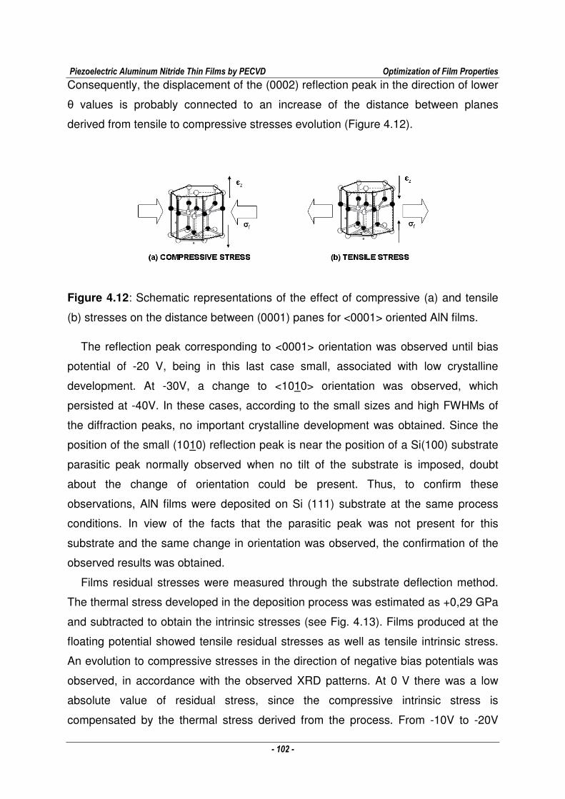
Piezoelectric Aluminum Nitride Thin Films by PECVD Optimization of Film Properties
- 102 -
Consequently, the displacement of the (0002) reflection peak in the direction of lower
θ values is probably connected to an increase of the distance between planes
derived from tensile to compressive stresses evolution (Figure 4.12).
Figure 4.12: Schematic representations of the effect of compressive (a) and tensile
(b) stresses on the distance between (0001) panes for <0001> oriented AlN films.
The reflection peak corresponding to <0001> orientation was observed until bias
potential of -20 V, being in this last case small, associated with low crystalline
development. At -30V, a change to <1010> orientation was observed, which
persisted at -40V. In these cases, according to the small sizes and high FWHMs of
the diffraction peaks, no important crystalline development was obtained. Since the
position of the small (1010) reflection peak is near the position of a Si(100) substrate
parasitic peak normally observed when no tilt of the substrate is imposed, doubt
about the change of orientation could be present. Thus, to confirm these
observations, AlN films were deposited on Si (111) substrate at the same process
conditions. In view of the facts that the parasitic peak was not present for this
substrate and the same change in orientation was observed, the confirmation of the
observed results was obtained.
Films residual stresses were measured through the substrate deflection method.
The thermal stress developed in the deposition process was estimated as +0,29 GPa
and subtracted to obtain the intrinsic stresses (see Fig. 4.13). Films produced at the
floating potential showed tensile residual stresses as well as tensile intrinsic stress.
An evolution to compressive stresses in the direction of negative bias potentials was
observed, in accordance with the observed XRD patterns. At 0 V there was a low
absolute value of residual stress, since the compressive intrinsic stress is
compensated by the thermal stress derived from the process. From -10V to -20V
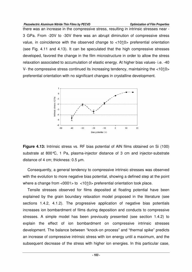
Piezoelectric Aluminum Nitride Thin Films by PECVD Optimization of Film Properties
- 103 -
there was an increase in the compressive stress, resulting in intrinsic stresses near -
3 GPa. From -20V to -30V there was an abrupt diminution of compressive stress
value, in coincidence with the observed change to <1010> preferential orientation
(see Fig. 4.11 and 4.13). It can be speculated that the high compressive stresses
developed, favored the change in the film microstructure in order to allow the stress
relaxation associated to accumulation of elastic energy. At higher bias values- i.e. -40
V- the compressive stress continued its increasing tendency, maintaining the <1010>
preferential orientation with no significant changes in crystalline development.
Figure 4.13: Intrinsic stress vs. RF bias potential of AlN films obtained on Si (100)
substrate at 800°C, 1 Pa, plasma-injector distance of 3 cm and injector-substrate
distance of 4 cm; thickness: 0.5 µm.
Consequently, a general tendency to compressive intrinsic stresses was observed
with the evolution to more negative bias potential, showing a defined step at the point
where a change from <0001> to <1010> preferential orientation took place.
Tensile stresses observed for films deposited at floating potential have been
explained by the grain boundary relaxation model proposed in the literature (see
sections 1.4.2, 4.1.2). The progressive application of negative bias potentials
increases ion bombardment of films during deposition and conducts to compressive
stresses. A simple model has been previously presented (see section 1.4.2) to
explain the effect of ion bombardment on compressive intrinsic stresses
development. The balance between “knock-on process” and “thermal spike” predicts
an increase of compressive intrinsic stress with ion energy until a maximum, and the
subsequent decrease of the stress with higher ion energies. In this particular case,
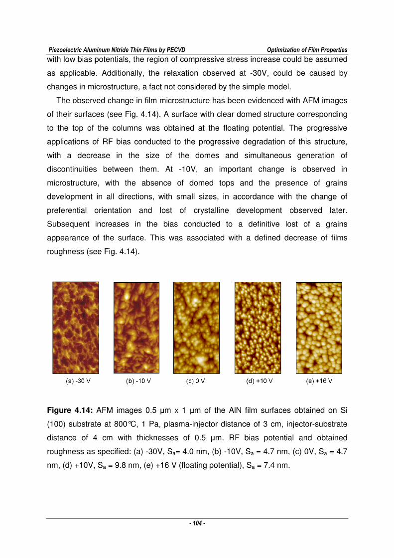
Piezoelectric Aluminum Nitride Thin Films by PECVD Optimization of Film Properties
- 104 -
with low bias potentials, the region of compressive stress increase could be assumed
as applicable. Additionally, the relaxation observed at -30V, could be caused by
changes in microstructure, a fact not considered by the simple model.
The observed change in film microstructure has been evidenced with AFM images
of their surfaces (see Fig. 4.14). A surface with clear domed structure corresponding
to the top of the columns was obtained at the floating potential. The progressive
applications of RF bias conducted to the progressive degradation of this structure,
with a decrease in the size of the domes and simultaneous generation of
discontinuities between them. At -10V, an important change is observed in
microstructure, with the absence of domed tops and the presence of grains
development in all directions, with small sizes, in accordance with the change of
preferential orientation and lost of crystalline development observed later.
Subsequent increases in the bias conducted to a definitive lost of a grains
appearance of the surface. This was associated with a defined decrease of films
roughness (see Fig. 4.14).
Figure 4.14: AFM images 0.5 µm x 1 µm of the AlN film surfaces obtained on Si
(100) substrate at 800°C, 1 Pa, plasma-injector distance of 3 cm, injector-substrate
distance of 4 cm with thicknesses of 0.5 µm. RF bias potential and obtained
roughness as specified: (a) -30V, Sa= 4.0 nm, (b) -10V, Sa = 4.7 nm, (c) 0V, Sa = 4.7
nm, (d) +10V, Sa = 9.8 nm, (e) +16 V (floating potential), Sa = 7.4 nm.
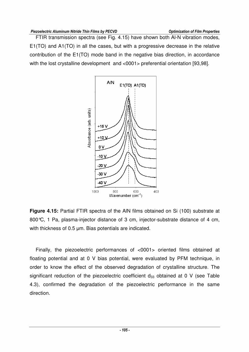
Piezoelectric Aluminum Nitride Thin Films by PECVD Optimization of Film Properties
- 105 -
FTIR transmission spectra (see Fig. 4.15) have shown both Al-N vibration modes,
E1(TO) and A1(TO) in all the cases, but with a progressive decrease in the relative
contribution of the E1(TO) mode band in the negative bias direction, in accordance
with the lost crystalline development and <0001> preferential orientation [93,98].
Figure 4.15: Partial FTIR spectra of the AlN films obtained on Si (100) substrate at
800°C, 1 Pa, plasma-injector distance of 3 cm, injector-substrate distance of 4 cm,
with thickness of 0.5 µm. Bias potentials are indicated.
Finally, the piezoelectric performances of <0001> oriented films obtained at
floating potential and at 0 V bias potential, were evaluated by PFM technique, in
order to know the effect of the observed degradation of crystalline structure. The
significant reduction of the piezoelectric coefficient d33 obtained at 0 V (see Table
4.3), confirmed the degradation of the piezoelectric performance in the same
direction.
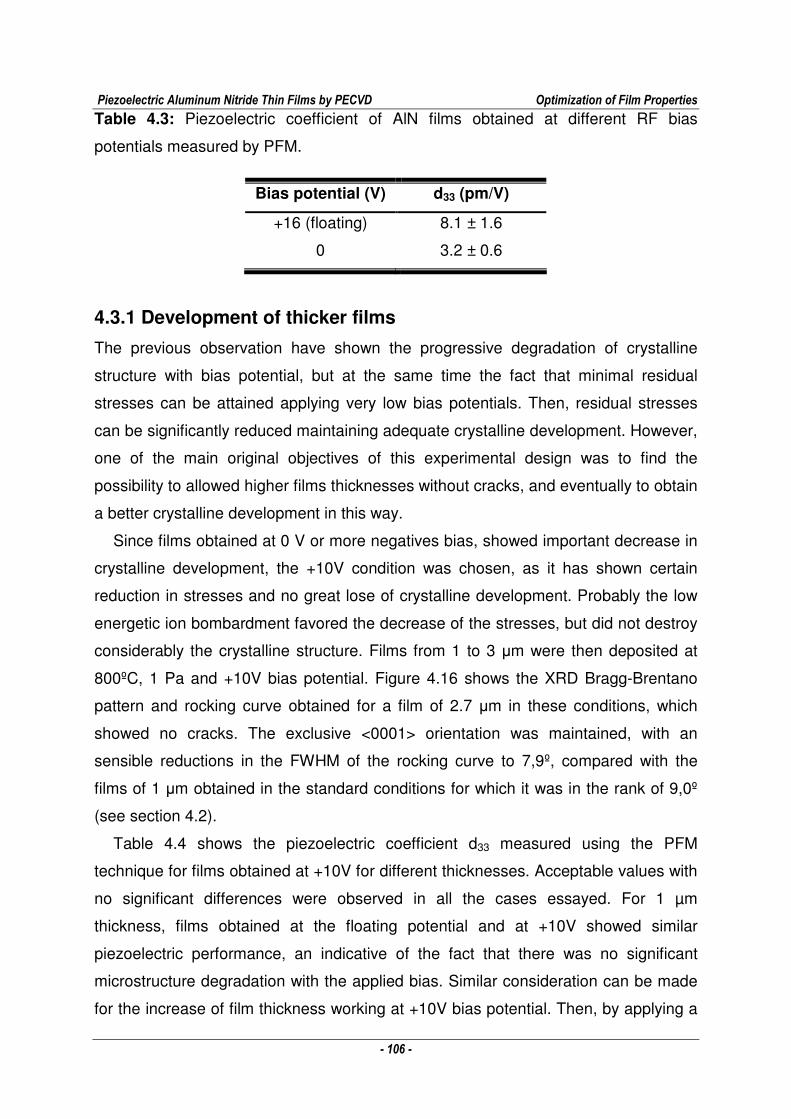
Piezoelectric Aluminum Nitride Thin Films by PECVD Optimization of Film Properties
- 106 -
Table 4.3: Piezoelectric coefficient of AlN films obtained at different RF bias
potentials measured by PFM.
Bias potential (V) d33 (pm/V)
+16 (floating) 8.1 ± 1.6
0 3.2 ± 0.6
4.3.1 Development of thicker films
The previous observation have shown the progressive degradation of crystalline
structure with bias potential, but at the same time the fact that minimal residual
stresses can be attained applying very low bias potentials. Then, residual stresses
can be significantly reduced maintaining adequate crystalline development. However,
one of the main original objectives of this experimental design was to find the
possibility to allowed higher films thicknesses without cracks, and eventually to obtain
a better crystalline development in this way.
Since films obtained at 0 V or more negatives bias, showed important decrease in
crystalline development, the +10V condition was chosen, as it has shown certain
reduction in stresses and no great lose of crystalline development. Probably the low
energetic ion bombardment favored the decrease of the stresses, but did not destroy
considerably the crystalline structure. Films from 1 to 3 µm were then deposited at
800ºC, 1 Pa and +10V bias potential. Figure 4.16 shows the XRD Bragg-Brentano
pattern and rocking curve obtained for a film of 2.7 µm in these conditions, which
showed no cracks. The exclusive <0001> orientation was maintained, with an
sensible reductions in the FWHM of the rocking curve to 7,9º, compared with the
films of 1 µm obtained in the standard conditions for which it was in the rank of 9,0º
(see section 4.2).
Table 4.4 shows the piezoelectric coefficient d33 measured using the PFM
technique for films obtained at +10V for different thicknesses. Acceptable values with
no significant differences were observed in all the cases essayed. For 1 µm
thickness, films obtained at the floating potential and at +10V showed similar
piezoelectric performance, an indicative of the fact that there was no significant
microstructure degradation with the applied bias. Similar consideration can be made
for the increase of film thickness working at +10V bias potential. Then, by applying a
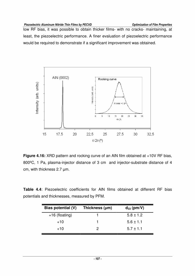
Piezoelectric Aluminum Nitride Thin Films by PECVD Optimization of Film Properties
- 107 -
low RF bias, it was possible to obtain thicker films- with no cracks- maintaining, at
least, the piezoelectric performance. A finer evaluation of piezoelectric performance
would be required to demonstrate if a significant improvement was obtained.
Figure 4.16: XRD pattern and rocking curve of an AlN film obtained at +10V RF bias,
800ºC, 1 Pa, plasma-injector distance of 3 cm and injector-substrate distance of 4
cm, with thickness 2.7 µm.
Table 4.4: Piezoelectric coefficients for AlN films obtained at different RF bias
potentials and thicknesses, measured by PFM.
Bias potential (V) Thickness (µm) d33 (pm/V)
+16 (floating) 1 5.8 ± 1.2
+10 1 5.6 ± 1.1
+10 2 5.7 ± 1.1
Piezoelectric Aluminum Nitride Thin Films by PECVD Optimization of Film Properties
- 108 -
4.4 Effect of the H2 addition to the reaction chamber
The addition of certain proportion of H2 to N2 plasmas has been used in the past to
increase the concentration of energetic species in reactor chambers [100]. Moreover,
it has been speculated about the favorable effect for AlN chemical vapor deposition
processes, because hydrogen can avoid the deposition of impurities with the film [61,
63]. In particular, the deposition of CN species with film would be avoided by the
generation of HCN species [61].
AlN films with thicknesses of 0.5 µm were prepared under the standard process
conditions- i.e. with N2 flow - and working with a N2/H2 flow in order to verify if effects
are observed in this sense. Figure 4.17 shows the XRD patterns obtained in both
cases. No improvement was observed with hydrogen addition, neither in diffraction
peak intensities nor in rocking curve FWHMs. These results were in accordance with
the OES plasma characterization discussed later (see section 4.6.2).
Figure 4.17: XRD patterns and rocking curves of the AlN films obtained at 800ºC, 1
Pa, no RF bias, plasma-injector distance of 3 cm and injector-substrate distance of 4
cm and depositions time 7 min. The plasma generating gas flows are indicated for
each case: N2 (125 sccm) or N2/H2 (112 sccm / 13 sccm).
Piezoelectric Aluminum Nitride Thin Films by PECVD Optimization of Film Properties
- 109 -
4.5 Optimal process conditions
The optimal process conditions to obtain <0001> and <1010> oriented films were
defined in accordance with the previous results (see Table 4.5). Low plasma injector
distance (3 cm), and high temperature (800ºC) were selected to obtain <0001>
oriented films at low pressures (1 Pa) and <1010> oriented films at high pressures (8
Pa). In order to reduce tensile residual stresses in films and/or to obtain thicknesses
higher than 1.5 µm, a low RF bias potential must be applied, changing the typical
values of +16 -+20 V (floating potential), to +10V.
Table 4.5: Optimal process conditions for AlN films deposition
Variable AlN film growth Microwave power (kW) 1.6 Nitrogen flow rate (sccm) 125 Argon flow rate (sccm) 50 TMA flow rate (sccm) 1 Plasma-injector distance dpi(cm) 3 Injector-substrate distance dis (cm) 4 RF bias potential (V) Floating* Substrate temperature (°C) 800 Chamber pressure (Pa) 1 (for <0001>oriented)
8 (for <1010> oriented)
*Until thickness of 1.5 µm, and +10V for thicker films until thickness of 2.5 µm
AlN films were deposited on whole Si(100) wafers under these process conditions
with the purpose of constructing SAW devices. Two thicknesses were obtained, 0.5
µm and 1 µm, in order to evaluate the effect of thickness on devices performance.
Films were finely characterized in microstructure and composition. Attention was
focused on certain characteristics that have been related in the past with the
piezoelectric performance: FWHM of the XRD rocking curve, E1(LO) and A1(LO)
vibration modes of Al-N observed by FTIR in reflection configuration and the
concentration of oxygen impurity in the film.
Fig. 4.18 shows the XRD pattern and rocking curve of the obtained films with
thickness 1 µm. While <0001> AlN films showed well crystalline development with
intense reflections peaks, and rocking curves with FWHM of 9.0º, <1010> AlN films
showed small reflection peaks, indicative of lower crystalline development, and
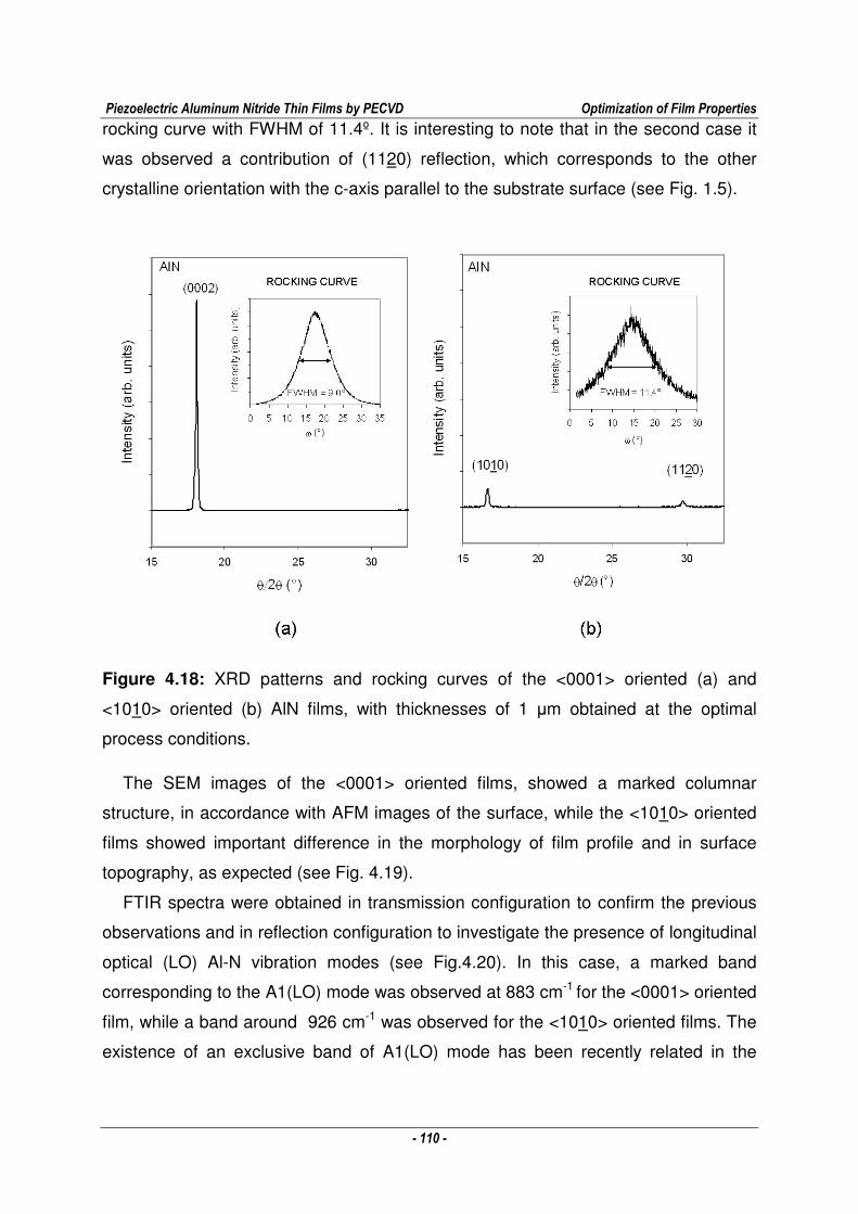
Piezoelectric Aluminum Nitride Thin Films by PECVD Optimization of Film Properties
- 110 -
rocking curve with FWHM of 11.4º. It is interesting to note that in the second case it
was observed a contribution of (1120) reflection, which corresponds to the other
crystalline orientation with the c-axis parallel to the substrate surface (see Fig. 1.5).
Figure 4.18: XRD patterns and rocking curves of the <0001> oriented (a) and
<1010> oriented (b) AlN films, with thicknesses of 1 µm obtained at the optimal
process conditions.
The SEM images of the <0001> oriented films, showed a marked columnar
structure, in accordance with AFM images of the surface, while the <1010> oriented
films showed important difference in the morphology of film profile and in surface
topography, as expected (see Fig. 4.19).
FTIR spectra were obtained in transmission configuration to confirm the previous
observations and in reflection configuration to investigate the presence of longitudinal
optical (LO) Al-N vibration modes (see Fig.4.20). In this case, a marked band
corresponding to the A1(LO) mode was observed at 883 cm-1 for the <0001> oriented
film, while a band around 926 cm-1 was observed for the <1010> oriented films. The
existence of an exclusive band of A1(LO) mode has been recently related in the
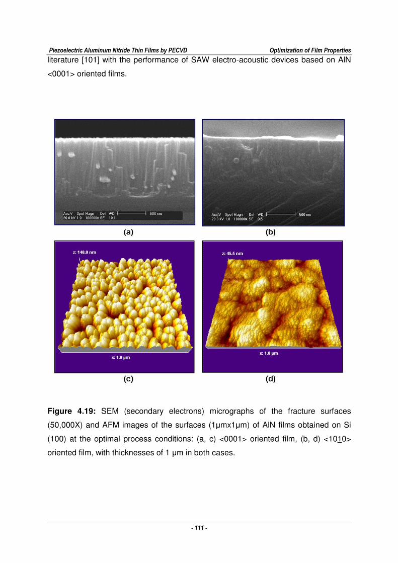
Piezoelectric Aluminum Nitride Thin Films by PECVD Optimization of Film Properties
- 111 -
literature [101] with the performance of SAW electro-acoustic devices based on AlN
<0001> oriented films.
Figure 4.19: SEM (secondary electrons) micrographs of the fracture surfaces
(50,000X) and AFM images of the surfaces (1µmx1µm) of AlN films obtained on Si
(100) at the optimal process conditions: (a, c) <0001> oriented film, (b, d) <1010>
oriented film, with thicknesses of 1 µm in both cases.
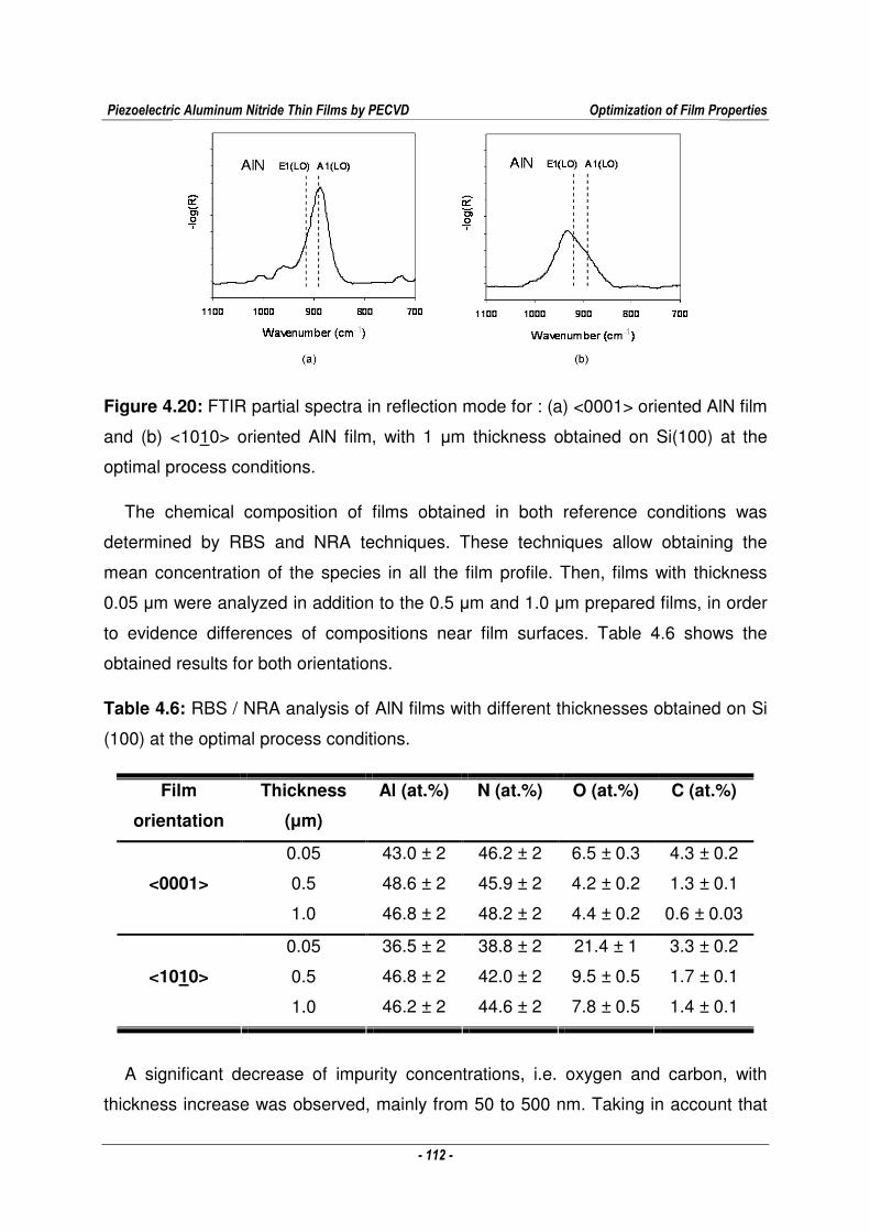
Piezoelectric Aluminum Nitride Thin Films by PECVD Optimization of Film Properties
- 112 -
Figure 4.20: FTIR partial spectra in reflection mode for : (a) <0001> oriented AlN film
and (b) <1010> oriented AlN film, with 1 µm thickness obtained on Si(100) at the
optimal process conditions.
The chemical composition of films obtained in both reference conditions was
determined by RBS and NRA techniques. These techniques allow obtaining the
mean concentration of the species in all the film profile. Then, films with thickness
0.05 µm were analyzed in addition to the 0.5 µm and 1.0 µm prepared films, in order
to evidence differences of compositions near film surfaces. Table 4.6 shows the
obtained results for both orientations.
Table 4.6: RBS / NRA analysis of AlN films with different thicknesses obtained on Si
(100) at the optimal process conditions.
Film
orientation
Thickness
(µm)
Al (at.%) N (at.%) O (at.%) C (at.%)
0.05 43.0 ± 2 46.2 ± 2 6.5 ± 0.3 4.3 ± 0.2
0.5 48.6 ± 2 45.9 ± 2 4.2 ± 0.2 1.3 ± 0.1
<0001>
1.0 46.8 ± 2 48.2 ± 2 4.4 ± 0.2 0.6 ± 0.03
0.05 36.5 ± 2 38.8 ± 2 21.4 ± 1 3.3 ± 0.2
0.5 46.8 ± 2 42.0 ± 2 9.5 ± 0.5 1.7 ± 0.1
<1010>
1.0 46.2 ± 2 44.6 ± 2 7.8 ± 0.5 1.4 ± 0.1
A significant decrease of impurity concentrations, i.e. oxygen and carbon, with
thickness increase was observed, mainly from 50 to 500 nm. Taking in account that
Piezoelectric Aluminum Nitride Thin Films by PECVD Optimization of Film Properties
- 113 -
these values correspond to mean concentrations in film profiles, the observed
evolutions can be associated with a region near film surfaces with higher impurity
values. In the case of oxygen this fact can be related with the spontaneous oxidation
of the AlN film surface after the deposition process under atmospheric conditions
[102, 60]. However, in the case of carbon, it is possible to speculate about two
possible reasons: first the adsorption of carbonated gases on the film surface in
contact with the environment and second the injection of residual quantities of TMA
(precursor) during the lines cleaning after the deposition process. XPS analysis
conducted on film surfaces, which corresponded approximately to 10 nm depths,
confirmed the elevated levels of aluminum oxide and carbon present in these cases.
Furthermore, the <1010> oriented films have shown oxygen concentration values
significantly higher than the <0001> oriented films (see Table 4.6). These differences
are consistent with the lower crystalline development evidenced by the XRD patterns
for <1010> oriented films. It can be speculated that higher process pressures allowed
higher concentrations of residual oxygen in the reactor chamber, which reacted with
aluminum instead of nitrogen and was incorporated to the film structure as aluminum
oxide.
Piezoelectric performance of the prepared films with 0.5 and 1 µm was evaluated
by PFM for both orientations. Optimal piezoelectric d33 values were obtained for
<0001> oriented films, as previously discussed (see section 4.2) and low or absence
of piezoelectric response was obtained for <1010> oriented films, as expected for
this configuration (see Appendix B).
4.5.1 Reproducibility of the MWPECVD technique
Three independent runs were conducted at both optimal process conditions in order
to know the reproducibility of the technique for development of film microstructures.
The obtained films for each process conditions have shown the same exclusive
orientation as well as similar levels of crystalline development in all the runs (see Fig.
4.21(a)). Furthermore, the quantifications of the orientation grade for the different
cases through the rocking curves have shown low dispersion (see Fig. 4.21(b)).
This high reproducibility of the technique had been observed in general for the
different process conditions tested.
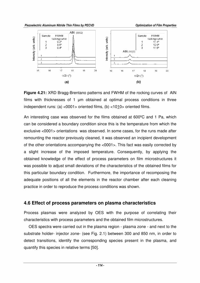
Piezoelectric Aluminum Nitride Thin Films by PECVD Optimization of Film Properties
- 114 -
Figure 4.21: XRD Bragg-Brentano patterns and FWHM of the rocking curves of AlN
films with thicknesses of 1 µm obtained at optimal process conditions in three
independent runs: (a) <0001> oriented films, (b) <1010> oriented films.
An interesting case was observed for the films obtained at 600ºC and 1 Pa, which
can be considered a boundary condition since this is the temperature from which the
exclusive <0001> orientations was observed. In some cases, for the runs made after
remounting the reactor previously cleaned, it was observed an incipient development
of the other orientations accompanying the <0001>. This fact was easily corrected by
a slight increase of the imposed temperature. Consequently, by applying the
obtained knowledge of the effect of process parameters on film microstructures it
was possible to adjust small deviations of the characteristics of the obtained films for
this particular boundary condition. Furthermore, the importance of recomposing the
adequate positions of all the elements in the reactor chamber after each cleaning
practice in order to reproduce the process conditions was shown.
4.6 Effect of process parameters on plasma characteristics
Process plasmas were analyzed by OES with the purpose of correlating their
characteristics with process parameters and the obtained film microstructures.
OES spectra were carried out in the plasma region - plasma zone - and next to the
substrate holder- injector zone- (see Fig. 2.1) between 300 and 850 nm, in order to
detect transitions, identify the corresponding species present in the plasma, and
quantify this species in relative terms [50].
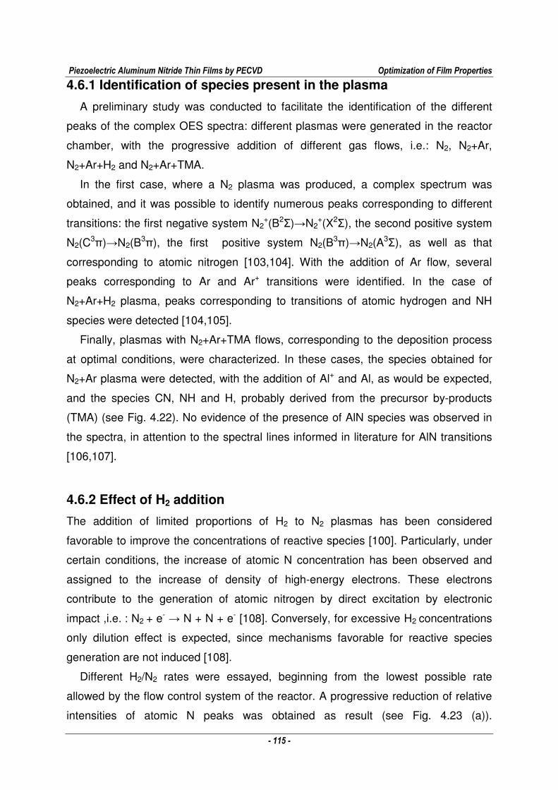
Piezoelectric Aluminum Nitride Thin Films by PECVD Optimization of Film Properties
- 115 -
4.6.1 Identification of species present in the plasma
A preliminary study was conducted to facilitate the identification of the different
peaks of the complex OES spectra: different plasmas were generated in the reactor
chamber, with the progressive addition of different gas flows, i.e.: N2, N2+Ar,
N2+Ar+H2 and N2+Ar+TMA.
In the first case, where a N2 plasma was produced, a complex spectrum was
obtained, and it was possible to identify numerous peaks corresponding to different
transitions: the first negative system N2+(B2Σ)→N2
+(X2Σ), the second positive system
N2(C3π)→N2(B
3π), the first positive system N2(B3π)→N2(A
3Σ), as well as that
corresponding to atomic nitrogen [103,104]. With the addition of Ar flow, several
peaks corresponding to Ar and Ar+ transitions were identified. In the case of
N2+Ar+H2 plasma, peaks corresponding to transitions of atomic hydrogen and NH
species were detected [104,105].
Finally, plasmas with N2+Ar+TMA flows, corresponding to the deposition process
at optimal conditions, were characterized. In these cases, the species obtained for
N2+Ar plasma were detected, with the addition of Al+ and Al, as would be expected,
and the species CN, NH and H, probably derived from the precursor by-products
(TMA) (see Fig. 4.22). No evidence of the presence of AlN species was observed in
the spectra, in attention to the spectral lines informed in literature for AlN transitions
[106,107].
4.6.2 Effect of H2 addition
The addition of limited proportions of H2 to N2 plasmas has been considered
favorable to improve the concentrations of reactive species [100]. Particularly, under
certain conditions, the increase of atomic N concentration has been observed and
assigned to the increase of density of high-energy electrons. These electrons
contribute to the generation of atomic nitrogen by direct excitation by electronic
impact ,i.e. : N2 + e- → N + N + e- [108]. Conversely, for excessive H2 concentrations
only dilution effect is expected, since mechanisms favorable for reactive species
generation are not induced [108].
Different H2/N2 rates were essayed, beginning from the lowest possible rate
allowed by the flow control system of the reactor. A progressive reduction of relative
intensities of atomic N peaks was obtained as result (see Fig. 4.23 (a)).
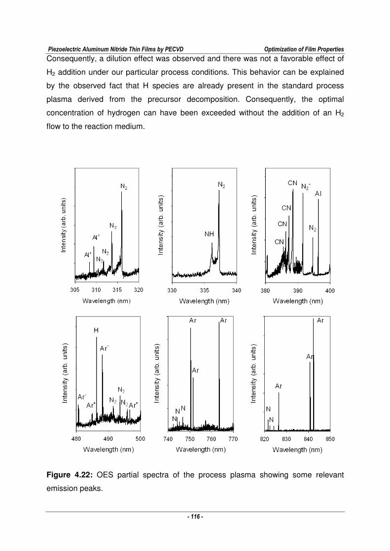
Piezoelectric Aluminum Nitride Thin Films by PECVD Optimization of Film Properties
- 116 -
Consequently, a dilution effect was observed and there was not a favorable effect of
H2 addition under our particular process conditions. This behavior can be explained
by the observed fact that H species are already present in the standard process
plasma derived from the precursor decomposition. Consequently, the optimal
concentration of hydrogen can have been exceeded without the addition of an H2
flow to the reaction medium.
Figure 4.22: OES partial spectra of the process plasma showing some relevant
emission peaks.
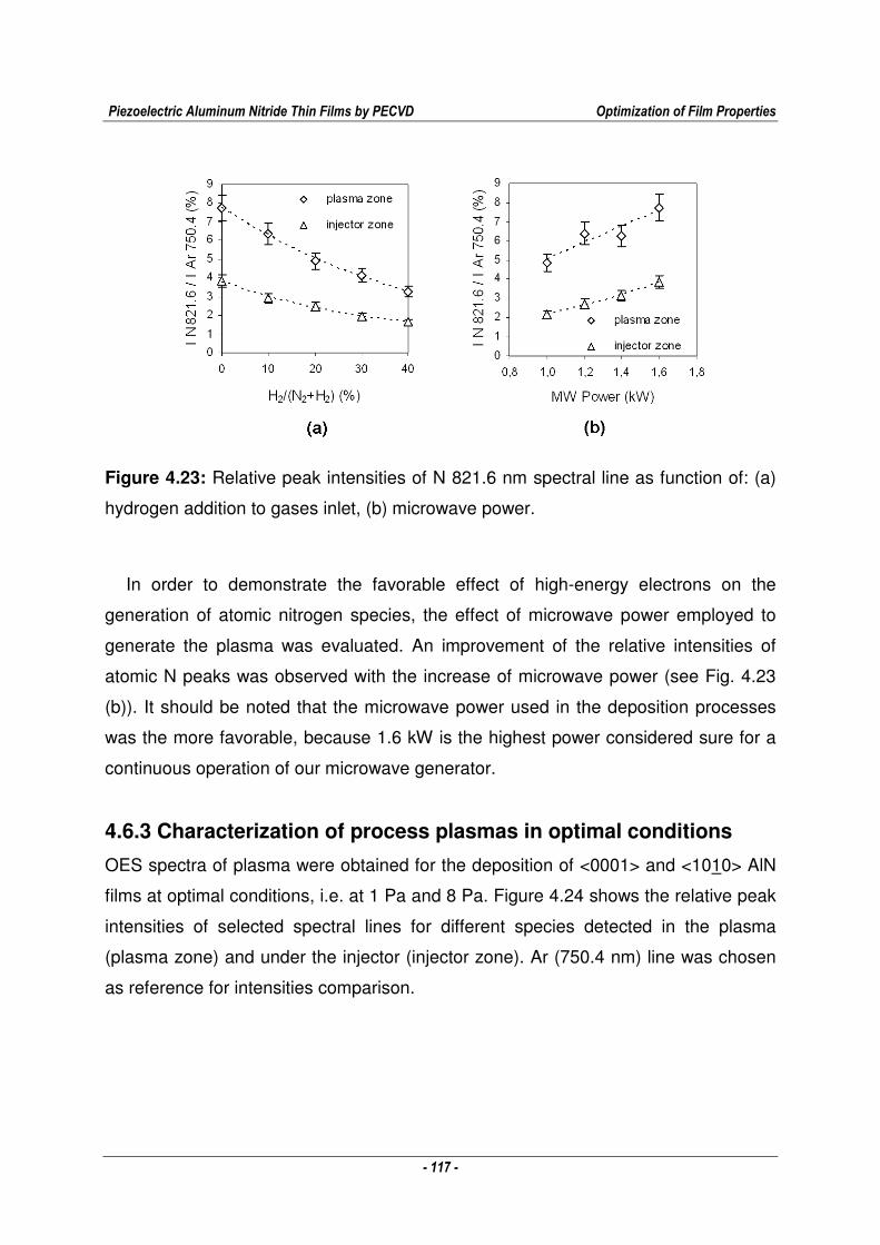
Piezoelectric Aluminum Nitride Thin Films by PECVD Optimization of Film Properties
- 117 -
Figure 4.23: Relative peak intensities of N 821.6 nm spectral line as function of: (a)
hydrogen addition to gases inlet, (b) microwave power.
In order to demonstrate the favorable effect of high-energy electrons on the
generation of atomic nitrogen species, the effect of microwave power employed to
generate the plasma was evaluated. An improvement of the relative intensities of
atomic N peaks was observed with the increase of microwave power (see Fig. 4.23
(b)). It should be noted that the microwave power used in the deposition processes
was the more favorable, because 1.6 kW is the highest power considered sure for a
continuous operation of our microwave generator.
4.6.3 Characterization of process plasmas in optimal conditions
OES spectra of plasma were obtained for the deposition of <0001> and <1010> AlN
films at optimal conditions, i.e. at 1 Pa and 8 Pa. Figure 4.24 shows the relative peak
intensities of selected spectral lines for different species detected in the plasma
(plasma zone) and under the injector (injector zone). Ar (750.4 nm) line was chosen
as reference for intensities comparison.
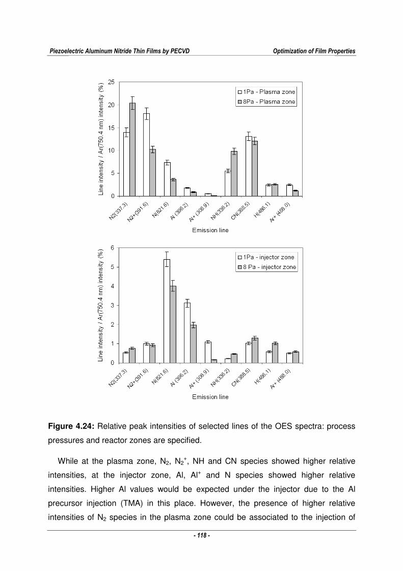
Piezoelectric Aluminum Nitride Thin Films by PECVD Optimization of Film Properties
- 118 -
Figure 4.24: Relative peak intensities of selected lines of the OES spectra: process
pressures and reactor zones are specified.
While at the plasma zone, N2, N2+, NH and CN species showed higher relative
intensities, at the injector zone, Al, Al+ and N species showed higher relative
intensities. Higher Al values would be expected under the injector due to the Al
precursor injection (TMA) in this place. However, the presence of higher relative
intensities of N2 species in the plasma zone could be associated to the injection of
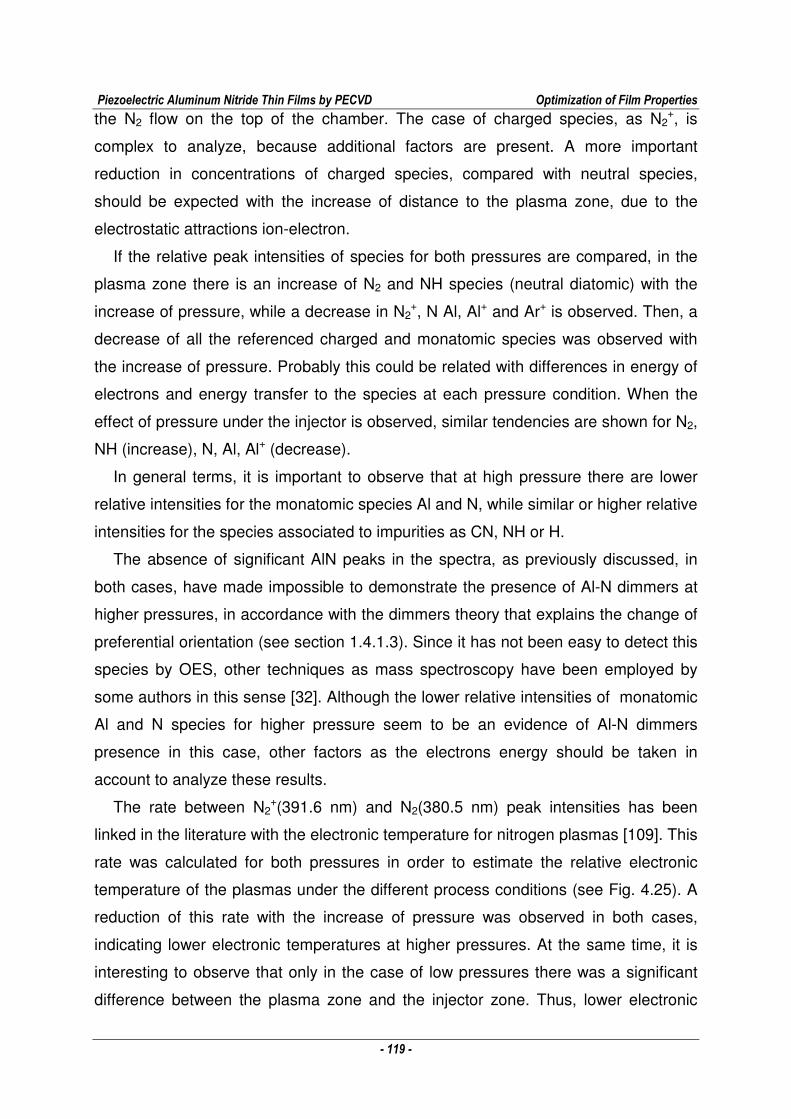
Piezoelectric Aluminum Nitride Thin Films by PECVD Optimization of Film Properties
- 119 -
the N2 flow on the top of the chamber. The case of charged species, as N2+, is
complex to analyze, because additional factors are present. A more important
reduction in concentrations of charged species, compared with neutral species,
should be expected with the increase of distance to the plasma zone, due to the
electrostatic attractions ion-electron.
If the relative peak intensities of species for both pressures are compared, in the
plasma zone there is an increase of N2 and NH species (neutral diatomic) with the
increase of pressure, while a decrease in N2+, N Al, Al+ and Ar+ is observed. Then, a
decrease of all the referenced charged and monatomic species was observed with
the increase of pressure. Probably this could be related with differences in energy of
electrons and energy transfer to the species at each pressure condition. When the
effect of pressure under the injector is observed, similar tendencies are shown for N2,
NH (increase), N, Al, Al+ (decrease).
In general terms, it is important to observe that at high pressure there are lower
relative intensities for the monatomic species Al and N, while similar or higher relative
intensities for the species associated to impurities as CN, NH or H.
The absence of significant AlN peaks in the spectra, as previously discussed, in
both cases, have made impossible to demonstrate the presence of Al-N dimmers at
higher pressures, in accordance with the dimmers theory that explains the change of
preferential orientation (see section 1.4.1.3). Since it has not been easy to detect this
species by OES, other techniques as mass spectroscopy have been employed by
some authors in this sense [32]. Although the lower relative intensities of monatomic
Al and N species for higher pressure seem to be an evidence of Al-N dimmers
presence in this case, other factors as the electrons energy should be taken in
account to analyze these results.
The rate between N2+(391.6 nm) and N2(380.5 nm) peak intensities has been
linked in the literature with the electronic temperature for nitrogen plasmas [109]. This
rate was calculated for both pressures in order to estimate the relative electronic
temperature of the plasmas under the different process conditions (see Fig. 4.25). A
reduction of this rate with the increase of pressure was observed in both cases,
indicating lower electronic temperatures at higher pressures. At the same time, it is
interesting to observe that only in the case of low pressures there was a significant
difference between the plasma zone and the injector zone. Thus, lower electronic
Piezoelectric Aluminum Nitride Thin Films by PECVD Optimization of Film Properties
- 120 -
temperatures for higher pressures could be associated to lower generation of atomic
species as N. This is in accordance with the lower peak intensities of atomic N and Al
species observed in this plasma at higher pressure. Consequently, the difference in
electronic temperatures could be related with the differences in the concentrations of
atomic Al and N species in the plasmas. Thus, it was not possible to evidence the
presence of Al-N dimmers at higher pressures, based on the lower concentrations of
the atomic species in the plasma.
Figure 4.25: Intensities rate between N2+(391.6nm) and N2(380.5nm) lines for the
OES spectra obtained at different process pressures and reactor zones.
The chemical analysis of the films (section 4.5) showed the presence of oxygen
impurity in their composition, with significant differences between both pressure
conditions. Therefore, it seemed relevant to look for evidences of oxygen species,
optically active, in the reaction media. No significant peaks were observed for the
typical spectral lines normally observed in oxygen plasmas, as atomic oxygen - e.g.:
777.2 nm - and O2+ first negative system - e.g.: 563.2 nm -, as well as oxygenated
species - AlO at 484 nm, OH at 310 nm - [53, 54]. Then, there was no evidence
about the presence of significant concentrations of oxygen in the reactor chamber
that could favor the contamination of the AlN film with oxygen during the deposition
process, at both pressures.
Piezoelectric Aluminum Nitride Thin Films by PECVD Application to Electroacoustic Devices
- 121 -
Chapter 5
APPLICATION TO ELECTROACOUSTIC
DEVICES
The optimization of properties of AlN films obtained by a microwave PECVD
technique in order to developed piezoelectric characteristics has been described in
the previous chapter. The construction of devices with AlN films obtained at optimal
conditions is shown in this chapter in order to determinate film performance in SAW
and BAW applications.
5.1 SAW devices
AlN films, with 0.5 µm and 1 µm thickness, were deposited on Si (100) wafers,- 100
mm diameters, 525 µm thickness, 5 Ohm.cm resistivity -, at optimal process
conditions (see section 4.5). After deposition, aluminum interdigital electrodes were
constructed on AlN films by a typical lithography process, in order to obtain SAW
devices with defined geometrical characteristics (see section 2.2.4.2). Figure 5.1
shows the obtained devices with typical wavelength of 20 µm. Therefore, the devices
were cut, mounted, and adequately connected to measure the frequency response
with a vector network analyzer HP8722ES.
5.1.1 Frequency response
The obtained whole frequency response of a SAW device based on a <0001>
oriented AlN film is shown in Fig. 5.2. The responses for S21 and S11 parameters are
specified, and the peaks associated to the piezoelectric response are clearly
identified.
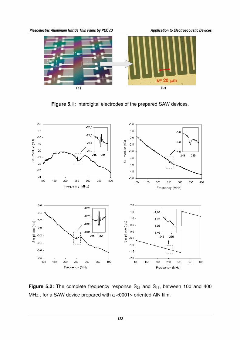
Piezoelectric Aluminum Nitride Thin Films by PECVD Application to Electroacoustic Devices
- 122 -
Figure 5.1: Interdigital electrodes of the prepared SAW devices.
Figure 5.2: The complete frequency response S21 and S11, between 100 and 400
MHz , for a SAW device prepared with a <0001> oriented AlN film.
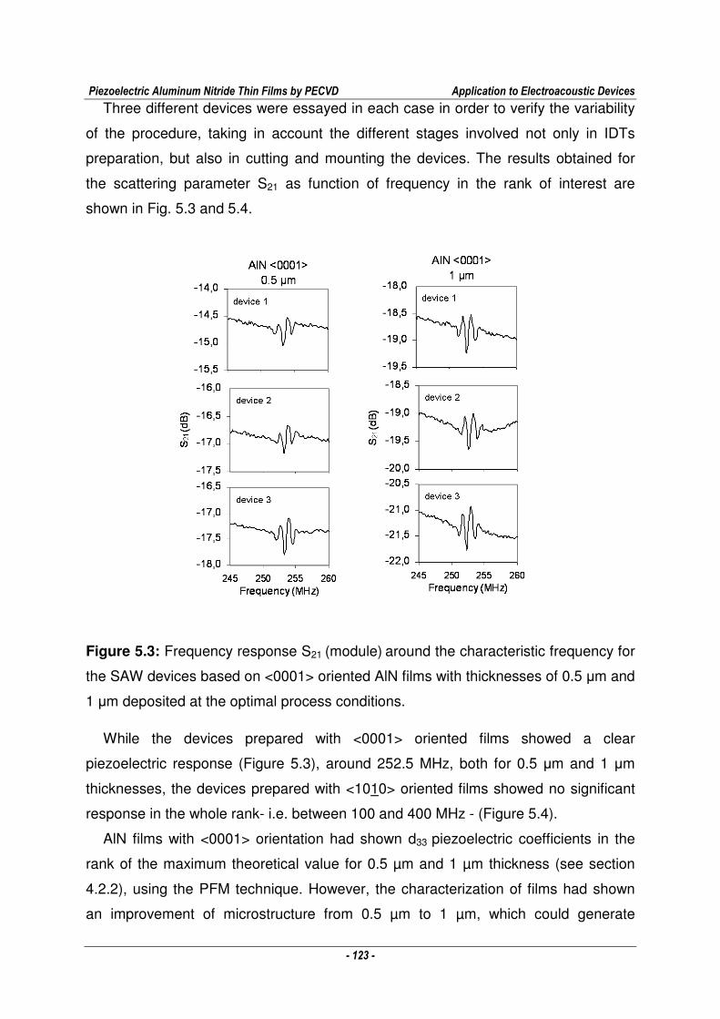
Piezoelectric Aluminum Nitride Thin Films by PECVD Application to Electroacoustic Devices
- 123 -
Three different devices were essayed in each case in order to verify the variability
of the procedure, taking in account the different stages involved not only in IDTs
preparation, but also in cutting and mounting the devices. The results obtained for
the scattering parameter S21 as function of frequency in the rank of interest are
shown in Fig. 5.3 and 5.4.
Figure 5.3: Frequency response S21 (module) around the characteristic frequency for
the SAW devices based on <0001> oriented AlN films with thicknesses of 0.5 µm and
1 µm deposited at the optimal process conditions.
While the devices prepared with <0001> oriented films showed a clear
piezoelectric response (Figure 5.3), around 252.5 MHz, both for 0.5 µm and 1 µm
thicknesses, the devices prepared with <1010> oriented films showed no significant
response in the whole rank- i.e. between 100 and 400 MHz - (Figure 5.4).
AlN films with <0001> orientation had shown d33 piezoelectric coefficients in the
rank of the maximum theoretical value for 0.5 µm and 1 µm thickness (see section
4.2.2), using the PFM technique. However, the characterization of films had shown
an improvement of microstructure from 0.5 µm to 1 µm, which could generate
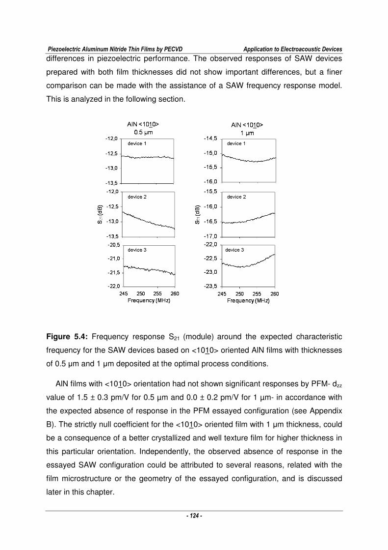
Piezoelectric Aluminum Nitride Thin Films by PECVD Application to Electroacoustic Devices
- 124 -
differences in piezoelectric performance. The observed responses of SAW devices
prepared with both film thicknesses did not show important differences, but a finer
comparison can be made with the assistance of a SAW frequency response model.
This is analyzed in the following section.
Figure 5.4: Frequency response S21 (module) around the expected characteristic
frequency for the SAW devices based on <1010> oriented AlN films with thicknesses
of 0.5 µm and 1 µm deposited at the optimal process conditions.
AlN films with <1010> orientation had not shown significant responses by PFM- dzz
value of 1.5 ± 0.3 pm/V for 0.5 µm and 0.0 ± 0.2 pm/V for 1 µm- in accordance with
the expected absence of response in the PFM essayed configuration (see Appendix
B). The strictly null coefficient for the <1010> oriented film with 1 µm thickness, could
be a consequence of a better crystallized and well texture film for higher thickness in
this particular orientation. Independently, the observed absence of response in the
essayed SAW configuration could be attributed to several reasons, related with the
film microstructure or the geometry of the essayed configuration, and is discussed
later in this chapter.
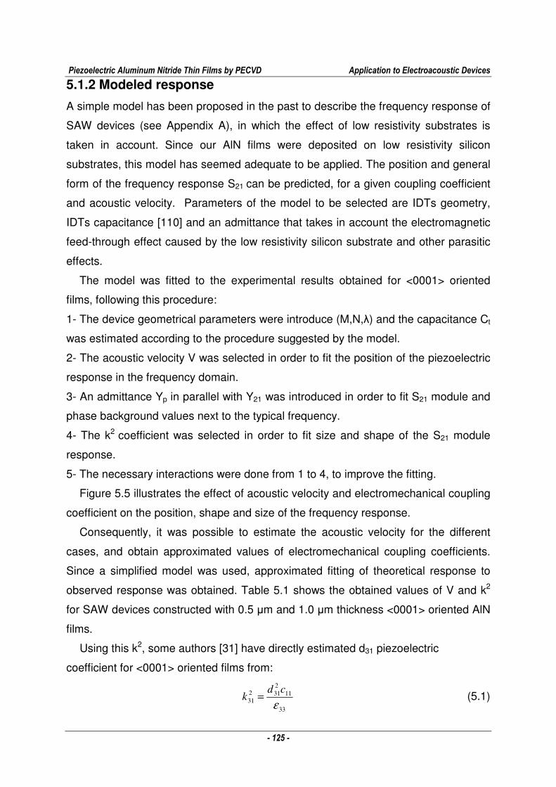
Piezoelectric Aluminum Nitride Thin Films by PECVD Application to Electroacoustic Devices
- 125 -
5.1.2 Modeled response
A simple model has been proposed in the past to describe the frequency response of
SAW devices (see Appendix A), in which the effect of low resistivity substrates is
taken in account. Since our AlN films were deposited on low resistivity silicon
substrates, this model has seemed adequate to be applied. The position and general
form of the frequency response S21 can be predicted, for a given coupling coefficient
and acoustic velocity. Parameters of the model to be selected are IDTs geometry,
IDTs capacitance [110] and an admittance that takes in account the electromagnetic
feed-through effect caused by the low resistivity silicon substrate and other parasitic
effects.
The model was fitted to the experimental results obtained for <0001> oriented
films, following this procedure:
1- The device geometrical parameters were introduce (M,N,λ) and the capacitance Ct
was estimated according to the procedure suggested by the model.
2- The acoustic velocity V was selected in order to fit the position of the piezoelectric
response in the frequency domain.
3- An admittance Yp in parallel with Y21 was introduced in order to fit S21 module and
phase background values next to the typical frequency.
4- The k2 coefficient was selected in order to fit size and shape of the S21 module
response.
5- The necessary interactions were done from 1 to 4, to improve the fitting.
Figure 5.5 illustrates the effect of acoustic velocity and electromechanical coupling
coefficient on the position, shape and size of the frequency response.
Consequently, it was possible to estimate the acoustic velocity for the different
cases, and obtain approximated values of electromechanical coupling coefficients.
Since a simplified model was used, approximated fitting of theoretical response to
observed response was obtained. Table 5.1 shows the obtained values of V and k2
for SAW devices constructed with 0.5 µm and 1.0 µm thickness <0001> oriented AlN
films.
Using this k2, some authors [31] have directly estimated d31 piezoelectric
coefficient for <0001> oriented films from:
33
112312
31ε
cdk = (5.1)
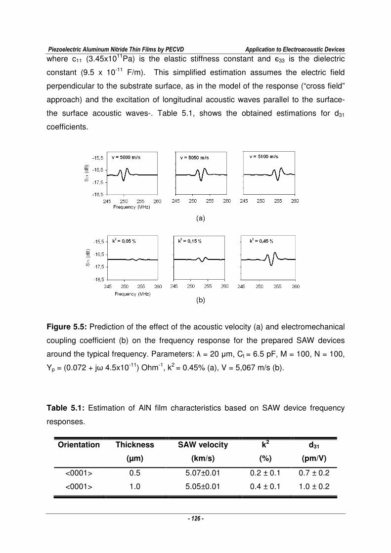
Piezoelectric Aluminum Nitride Thin Films by PECVD Application to Electroacoustic Devices
- 126 -
where c11 (3.45x10¹¹Pa) is the elastic stiffness constant and є33 is the dielectric
constant (9.5 x 10⁻¹¹ F/m). This simplified estimation assumes the electric field
perpendicular to the substrate surface, as in the model of the response (“cross field”
approach) and the excitation of longitudinal acoustic waves parallel to the surface-
the surface acoustic waves-. Table 5.1, shows the obtained estimations for d31
coefficients.
Figure 5.5: Prediction of the effect of the acoustic velocity (a) and electromechanical
coupling coefficient (b) on the frequency response for the prepared SAW devices
around the typical frequency. Parameters: λ = 20 µm, Ct = 6.5 pF, M = 100, N = 100,
Yp = (0.072 + jω 4.5x10⁻¹¹) Ohm-1, k2 = 0.45% (a), V = 5,067 m/s (b).
Table 5.1: Estimation of AlN film characteristics based on SAW device frequency
responses.
Orientation Thickness
(µm)
SAW velocity
(km/s)
k2
(%)
d31
(pm/V)
<0001> 0.5 5.07±0.01 0.2 ± 0.1 0.7 ± 0.2
<0001> 1.0 5.05±0.01 0.4 ± 0.1 1.0 ± 0.2
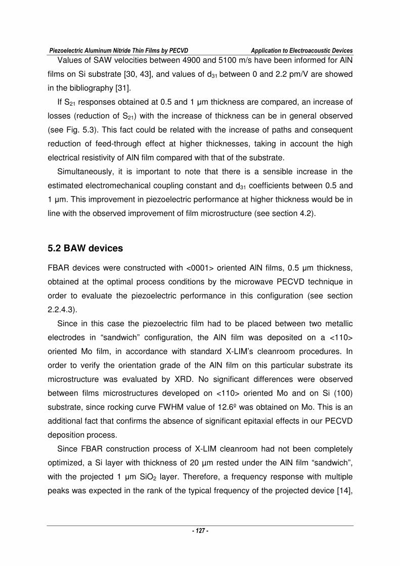
Piezoelectric Aluminum Nitride Thin Films by PECVD Application to Electroacoustic Devices
- 127 -
Values of SAW velocities between 4900 and 5100 m/s have been informed for AlN
films on Si substrate [30, 43], and values of d31 between 0 and 2.2 pm/V are showed
in the bibliography [31].
If S21 responses obtained at 0.5 and 1 µm thickness are compared, an increase of
losses (reduction of S21) with the increase of thickness can be in general observed
(see Fig. 5.3). This fact could be related with the increase of paths and consequent
reduction of feed-through effect at higher thicknesses, taking in account the high
electrical resistivity of AlN film compared with that of the substrate.
Simultaneously, it is important to note that there is a sensible increase in the
estimated electromechanical coupling constant and d31 coefficients between 0.5 and
1 µm. This improvement in piezoelectric performance at higher thickness would be in
line with the observed improvement of film microstructure (see section 4.2).
5.2 BAW devices
FBAR devices were constructed with <0001> oriented AlN films, 0.5 µm thickness,
obtained at the optimal process conditions by the microwave PECVD technique in
order to evaluate the piezoelectric performance in this configuration (see section
2.2.4.3).
Since in this case the piezoelectric film had to be placed between two metallic
electrodes in “sandwich” configuration, the AlN film was deposited on a <110>
oriented Mo film, in accordance with standard X-LIM’s cleanroom procedures. In
order to verify the orientation grade of the AlN film on this particular substrate its
microstructure was evaluated by XRD. No significant differences were observed
between films microstructures developed on <110> oriented Mo and on Si (100)
substrate, since rocking curve FWHM value of 12.6º was obtained on Mo. This is an
additional fact that confirms the absence of significant epitaxial effects in our PECVD
deposition process.
Since FBAR construction process of X-LIM cleanroom had not been completely
optimized, a Si layer with thickness of 20 µm rested under the AlN film “sandwich”,
with the projected 1 µm SiO2 layer. Therefore, a frequency response with multiple
peaks was expected in the rank of the typical frequency of the projected device [14],
Piezoelectric Aluminum Nitride Thin Films by PECVD Application to Electroacoustic Devices
- 128 -
in place of the single response obtained in standard FBAR resonators (see Appendix
A). Figure 5.6 shows a general view and dimensions of the prepared devices.
Figure 5.6: General view of a prepared FBAR device.
5.2.1 Frequency response
Figure 5.7 (a) shows the frequency response of the device between 0.5 and 8.5
GHz, where several peaks in the rank of 3 GHz are observed, corresponding to the
resonance frequency of the first harmonic- i.e. λ/2-. A second resonance mode was
observed around 9 GHz (see Fig. 5.7 (b)) which confirms the piezoelectric response
of the film. As only the odd modes are excited in this type of devices, this second
mode corresponds to 3λ/2 [15].
5.2.2 Modeled response
The one-dimensional model developed for BAW free resonators in Appendix 1 shows
only an approximated frequency response of FBAR configurations. FBAR devices for
high frequencies must be strictly modeled considering not only the piezoelectric film
but also the whole geometry of the device, including the electrodes and other layers,
since their thicknesses are significant [11, 15]. Since the thickness of the metallic Mo
electrodes were 400 nm, the AlN film 500nm, and the SiO2 layer 300 nm, the half
wavelength associated to the total thickness would correspond to approximately 1.6
µm, in a first approach. If the acoustic velocity of bulk acoustic waves in AlN from
bibliography is supposed- i.e. 10,400 m/s-, the resonance frequency associated to
the first harmonic should be in the rank of 3 GHz. This corresponds to the observed
value in the measured device’s frequency response.
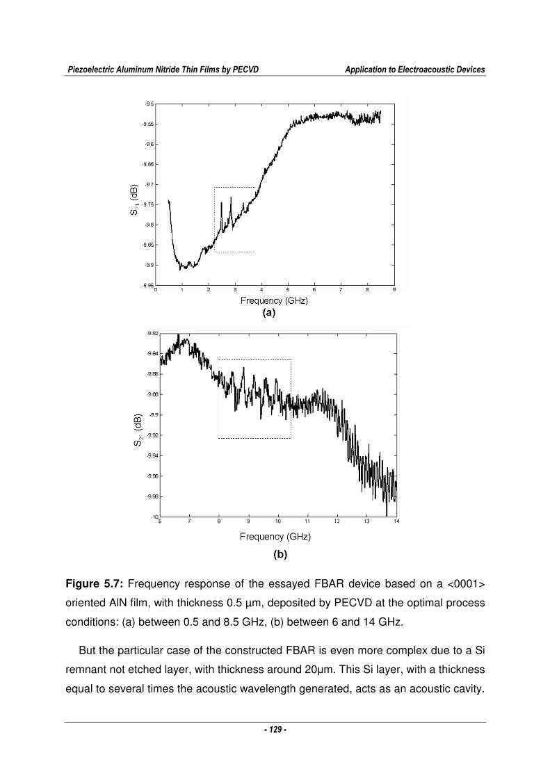
Piezoelectric Aluminum Nitride Thin Films by PECVD Application to Electroacoustic Devices
- 129 -
Figure 5.7: Frequency response of the essayed FBAR device based on a <0001>
oriented AlN film, with thickness 0.5 µm, deposited by PECVD at the optimal process
conditions: (a) between 0.5 and 8.5 GHz, (b) between 6 and 14 GHz.
But the particular case of the constructed FBAR is even more complex due to a Si
remnant not etched layer, with thickness around 20µm. This Si layer, with a thickness
equal to several times the acoustic wavelength generated, acts as an acoustic cavity.
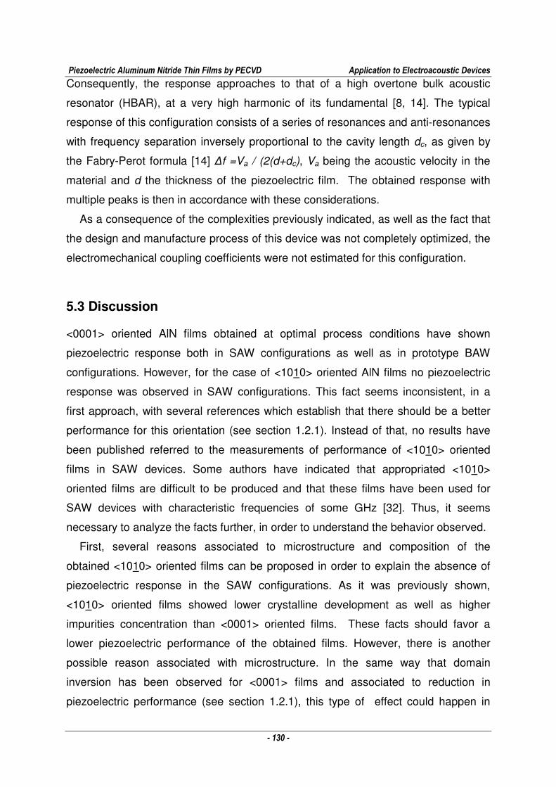
Piezoelectric Aluminum Nitride Thin Films by PECVD Application to Electroacoustic Devices
- 130 -
Consequently, the response approaches to that of a high overtone bulk acoustic
resonator (HBAR), at a very high harmonic of its fundamental [8, 14]. The typical
response of this configuration consists of a series of resonances and anti-resonances
with frequency separation inversely proportional to the cavity length dc, as given by
the Fabry-Perot formula [14] ∆f =Va / (2(d+dc), Va being the acoustic velocity in the
material and d the thickness of the piezoelectric film. The obtained response with
multiple peaks is then in accordance with these considerations.
As a consequence of the complexities previously indicated, as well as the fact that
the design and manufacture process of this device was not completely optimized, the
electromechanical coupling coefficients were not estimated for this configuration.
5.3 Discussion
<0001> oriented AlN films obtained at optimal process conditions have shown
piezoelectric response both in SAW configurations as well as in prototype BAW
configurations. However, for the case of <1010> oriented AlN films no piezoelectric
response was observed in SAW configurations. This fact seems inconsistent, in a
first approach, with several references which establish that there should be a better
performance for this orientation (see section 1.2.1). Instead of that, no results have
been published referred to the measurements of performance of <1010> oriented
films in SAW devices. Some authors have indicated that appropriated <1010>
oriented films are difficult to be produced and that these films have been used for
SAW devices with characteristic frequencies of some GHz [32]. Thus, it seems
necessary to analyze the facts further, in order to understand the behavior observed.
First, several reasons associated to microstructure and composition of the
obtained <1010> oriented films can be proposed in order to explain the absence of
piezoelectric response in the SAW configurations. As it was previously shown,
<1010> oriented films showed lower crystalline development as well as higher
impurities concentration than <0001> oriented films. These facts should favor a
lower piezoelectric performance of the obtained films. However, there is another
possible reason associated with microstructure. In the same way that domain
inversion has been observed for <0001> films and associated to reduction in
piezoelectric performance (see section 1.2.1), this type of effect could happen in
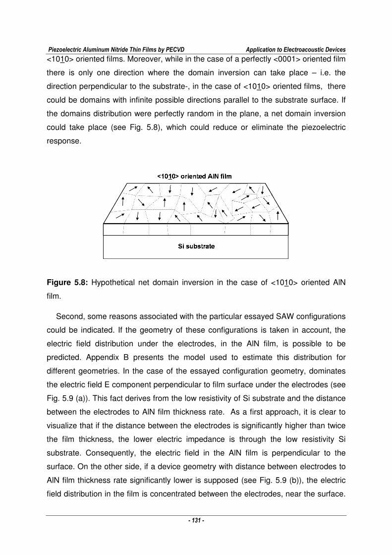
Piezoelectric Aluminum Nitride Thin Films by PECVD Application to Electroacoustic Devices
- 131 -
<1010> oriented films. Moreover, while in the case of a perfectly <0001> oriented film
there is only one direction where the domain inversion can take place – i.e. the
direction perpendicular to the substrate-, in the case of <1010> oriented films, there
could be domains with infinite possible directions parallel to the substrate surface. If
the domains distribution were perfectly random in the plane, a net domain inversion
could take place (see Fig. 5.8), which could reduce or eliminate the piezoelectric
response.
Figure 5.8: Hypothetical net domain inversion in the case of <1010> oriented AlN
film.
Second, some reasons associated with the particular essayed SAW configurations
could be indicated. If the geometry of these configurations is taken in account, the
electric field distribution under the electrodes, in the AlN film, is possible to be
predicted. Appendix B presents the model used to estimate this distribution for
different geometries. In the case of the essayed configuration geometry, dominates
the electric field E component perpendicular to film surface under the electrodes (see
Fig. 5.9 (a)). This fact derives from the low resistivity of Si substrate and the distance
between the electrodes to AlN film thickness rate. As a first approach, it is clear to
visualize that if the distance between the electrodes is significantly higher than twice
the film thickness, the lower electric impedance is through the low resistivity Si
substrate. Consequently, the electric field in the AlN film is perpendicular to the
surface. On the other side, if a device geometry with distance between electrodes to
AlN film thickness rate significantly lower is supposed (see Fig. 5.9 (b)), the electric
field distribution in the film is concentrated between the electrodes, near the surface.
Piezoelectric Aluminum Nitride Thin Films by PECVD Application to Electroacoustic Devices
- 132 -
Thus, there is a higher contribution of the electric field E component parallel to the
surface. This hypothetical situation corresponds to thicker AlN films with the same
IDTs geometry - and consequently the same typical frequency -, or to smaller IDTs-
and consequently higher typical frequency-, if the film thickness is maintained. It
should be also noted that, if the AlN film is deposited on a non conductive substrate
or non conductive thick film, the second situation is applicable. Obviously, it is
applicable as well, if AlN single crystal substrates instead of films are used.
When the piezoelectric response of an AlN crystal under the presence of an
electric field is analyzed (see Appendix I) higher piezoelectric coupling is obtained
once the E field is applied in the c-axis direction, corresponding to the d33 coefficient.
Thus, in order to generate surface acoustic waves through the piezoelectric effect in
a <1010> oriented AlN film, i.e. with the c-axis parallel to the surface, the presence of
E field component parallel to the surface in the piezoelectric film is relevant to obtain
an adequate response. Consequently, the essayed configuration, that corresponds to
the case shows in Fig. 5.9 (a), does not favor the optimal piezoelectric coupling of the
AlN <1010> oriented films.
Finally, as we have observed for the piezoelectric response of <0001> aluminum
nitride SAW devices, the effect of working with a low resistivity Si substrate produced
an important feedthrough effect, reducing the relative size of the response around the
characteristic frequency (Appendix A). If the response in this case were low,
associated with the previously indicated reasons, it would become probably
undetectable due to this particular effect.
The construction of a SAW device that could eliminate the discussed effects and
show the piezoelectric performance of the deposited <1010> films is out of the
objectives of the present work. Nevertheless, it is interesting to discuss which would
be the different options to conduct the work. First it is possible to think in smaller
IDTs, that means higher frequencies. If film thickness of 1 µm is maintained,
distances between fingers lower than 1 µm should be considered, that means fingers
of around 0.5 µm wide. They are possible to be constructed, but require more
sophisticated processes, being in the limit of the traditional microtechnology. In order
not to reduce so much the electrodes size, the AlN film thickness could be increased.
As was demonstrated for <0001> oriented films, it would be possible to arrive to
appropriated thicker films, - i.e. 3 µm or more-, acting on the RF-bias potential during
Piezoelectric Aluminum Nitride Thin Films by PECVD Application to Electroacoustic Devices
- 133 -
the deposition process if necessary. Last of all, other possibility to favor the
piezoelectric evaluation of <1010> oriented films would be the deposition on a non
conductive substrate.
Figure 5.9: Schematic representation of the electric field under two adjacent fingers
of interdigital electrode of a SAW device, supposing the AlN film deposited on a
substrate with low resistivity: (a) AlN film thickness substantially lower than the
distance between the electrodes, (b) AlN film thickness substantially higher than the
distance between electrodes.
Piezoelectric Aluminum Nitride Thin Films by PECVD Comparison with a PVD Technique
- 134 -
Chapter 6
COMPARISON WITH A PVD
TECHNIQUE
The previous chapters have shown the optimal process conditions to obtain
piezoelectric AlN films using a microwave PECVD technique. Also, the piezoelectric
performance of the obtained films in electro-acoustic applications, as SAW and BAW,
was verified. Since PVD sputtering has been the most investigated technique in the
past, a comparison of the films obtained by this process and the PECVD process has
seemed interesting to be conducted. In order to make this comparison, AlN thin films
prepared at the “Institut des Materiaux de Nantes”, using a PVD reactive sputtering
technique, were chosen.
6.1 PVD sputtering
<0001> oriented films were first obtained using a PVD sputtering reactor equipped
with a magnetron cathode and a DC generator. The standard process conditions
essayed where the following: PN2 / (PAr + PN2) = 0.3, distance substrate-target = 3 cm,
total pressure of 0.4 Pa, temperature < 200°C and deposition rate = 35 nm/min. The
obtained films showed orientation grades quantified by the rocking curve FWHM in
the rank of 7°. The evaluation of microstructure of film profiles by HRTEM and SAED
showed columnar shapes and the improvement of the crystalline quality with film
thickness. After a 5 nm amorphous interface, the microstructure changed from
misalignment angle of 23° to 6° in 1.5 µm thickness for the (0002) reflection. The
measured oxygen concentration in the films was 5.2 % [111].
Piezoelectric Aluminum Nitride Thin Films by PECVD Comparison with a PVD Technique
- 135 -
All these observations indicate that films obtained under these conditions by PVD
sputtering have not shown important differences with PECVD films, in relation with
their properties for piezoelectric applications. Moreover, a stricter comparison of the
evolution of crystalline quality and orientation grade in film profiles by SAED,
indicated a better quality of PECVD films (see section 4.2.1).
When the deposition conditions of both processes are compared, an important
difference of substrate temperatures is observed. While for PECVD process,
substrate temperatures over 600°C - i.e. real temperature over 500°C -, were
employed in order to obtain <0001> oriented AlN films, in the case of PVD process
the films were obtained at temperatures under 200°C. It is possible to speculate that
different factors favor diffusion effects and consequently crystalline development in
each deposition technique: high substrate temperature in the PECVD process and
high kinetic energies of sputtered species reaching the film surface in PVD process
[74, 112]. Consequently, adequate crystalline development would be possible to be
obtained by PVD technique at lower substrate temperatures.
Simultaneously, the change of preferential orientation from <0001> to <1010>, by
increasing the total pressure from 0.4 Pa to 0.8 Pa, was observed for the PVD
depositions technique. This similitude between both techniques confirms the
importance of the effect of the mean free path in the control of film orientations,
independently of the deposition process (see section 3.4).
The use of increasing bias potentials of substrate holder in the PVD process,
going from 0 to -200V have shown a reduction in the film crystalline development,
and at a certain level (-150 V), the change in the preferential orientations to <1010>
[74]. This is another important similitude in the observed behavior of both techniques.
Nevertheless, the bias value for orientation change in the case of the PECVD
technique was significantly lower (-20 V) (see section 4.3).
Since AlN films contamination with oxygen had been previously related with their
microstructures and piezoelectric performances [19, 37], the PVD process previously
described was improved in order to reduce this contamination. With the purpose of
arriving to this objective, two important changes were made: a) the vacuum system
was improved to arrive to lower residual pressures (10-4 Pa), and consequently lower
oxygen concentration in the reactor chamber before the deposition process, b) the
deposition rate was increased by rising the power applied to the target (70 nm/min),
Piezoelectric Aluminum Nitride Thin Films by PECVD Comparison with a PVD Technique
- 136 -
c) the ion to neutral species rate in the reaction medium was increased significantly
as a consequence of the increase of the magnetic field of the magnetron [111].
These changes introduced in the PVD technique allowed obtaining film orientation
grades corresponding to rocking curve FWHM in the rank of 2°, and at the same time
allowed to reduce the oxygen content to 0.4%. The evaluation of film microstructure
by HRTEM showed a dense columnar structure. The SAED confirmed the significant
improvement in the texture showing single crystal patterns in all the film profile [111].
These significant differences, which should be related with an increase in the
piezoelectric performance, were associated to reduction of the oxygen content.
Furthermore, these PVD films showed roughness values (Sa) lower than 1 nm and
compressive residual stresses- e.g.: -1 GPa for 0.5 µm thickness.
6.2 Piezoelectric performance
In order to evaluate the piezoelectric performance of the films obtained by the PVD
technique in electroacoustic devices, and at the same time to compare them with the
films obtained by the PECVD technique, BAW devices were prepared as was
previously described (see section 2.2.4.3). Figure 6.1 shows the XRD patterns of 0.5
µm AlN films deposited on <110> oriented Mo film for the construction of these BAW
devices.
The XRD patterns of both films showed exclusive <0001> orientation, but a higher
intensity of the (0002) reflection peak was observed for the PVD film. This fact could
be related with a higher crystalline development of the PVD films. At the same time
the evaluation of the orientation grade by rocking curve showed a FWHM significantly
lower for the PVD film, in the rank of 4.5°, indicative of a better texture development.
The evaluations of the frequency response of BAW devices prepared with the PVD
film showed a first resonance mode in the rank of 3 GHz, and the second resonance
mode in the rank of 9 GHz (see Fig. 6.2). These were the expected frequencies as a
function of the geometry and properties of the materials, and they were similar to the
case of the PECVD films (see Fig. 5.7). Taking in account the consideration done for
the construction of the BAW devices with PECVD films (see section 5.2), multiple
peaks were expected.
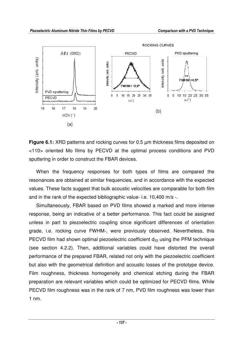
Piezoelectric Aluminum Nitride Thin Films by PECVD Comparison with a PVD Technique
- 137 -
Figure 6.1: XRD patterns and rocking curves for 0.5 µm thickness films deposited on
<110> oriented Mo films by PECVD at the optimal process conditions and PVD
sputtering in order to construct the FBAR devices.
When the frequency responses for both types of films are compared the
resonances are obtained at similar frequencies, and in accordance with the expected
values. These facts suggest that bulk acoustic velocities are comparable for both film
and in the rank of the expected bibliographic value- i.e. 10,400 m/s -.
Simultaneously, FBAR based on PVD films showed a marked and more intense
response, being an indicative of a better performance. This fact could be assigned
unless in part to piezoelectric coupling since significant differences of orientation
grade, i.e. rocking curve FWHM-, were previously observed. Nevertheless, this
PECVD film had shown optimal piezoelectric coefficient d33 using the PFM technique
(see section 4.2.2). Then, additional variables could have distorted the overall
performance of the prepared FBAR, related not only with the piezoelectric coefficient
but also with the geometrical definition and acoustic losses of the prototype device.
Film roughness, thickness homogeneity and chemical etching during the FBAR
preparation are relevant variables which could be optimized for PECVD films. While
PECVD film roughness was in the rank of 7 nm, PVD film roughness was lower than
1 nm.
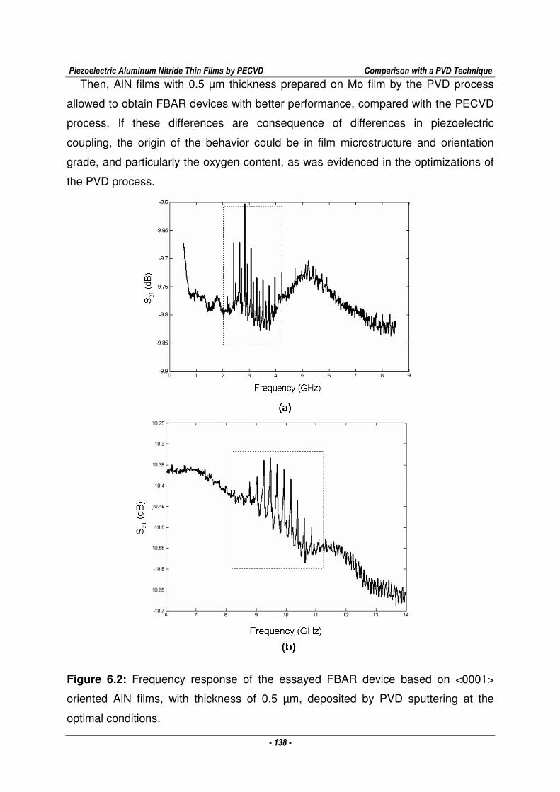
Piezoelectric Aluminum Nitride Thin Films by PECVD Comparison with a PVD Technique
- 138 -
Then, AlN films with 0.5 µm thickness prepared on Mo film by the PVD process
allowed to obtain FBAR devices with better performance, compared with the PECVD
process. If these differences are consequence of differences in piezoelectric
coupling, the origin of the behavior could be in film microstructure and orientation
grade, and particularly the oxygen content, as was evidenced in the optimizations of
the PVD process.
Figure 6.2: Frequency response of the essayed FBAR device based on <0001>
oriented AlN films, with thickness of 0.5 µm, deposited by PVD sputtering at the
optimal conditions.
Piezoelectric Aluminum Nitride Thin Films by PECVD Comparison with a PVD Technique
- 139 -
6.3 Discussion
The PECVD technique has allowed to obtain polycrystalline AlN films, as well as to
control their preferential orientation. The substrate temperature has been a relevant
variable to improve the crystalline development of the films as well as to allow the
development of texture and piezoelectric response, particularly for <0001> oriented
AlN film at low pressures.
The PVD sputtering technique has allowed obtaining similar results in film
microstructure at lower substrate temperatures, under standard conditions. The
optimization of this process conducted to significant improvement of obtained films.
The evaluation of FBAR devices constructed with 0.5µm films obtained using both
techniques have shown BAW velocities in the same rank and a more consistent
piezoelectric response for PVD films. This difference can be related, among other
reasons, with observed differences in the microstructure, evidenced by the XRD
patterns and rocking curves as well as the oxygen content in both cases.
It has been speculated in this work that the high kinetic energy of the sputtered
species in the PVD technique provided the necessary energy to allow the diffusion in
the surface during deposition and the crystallization of the film. Simultaneously, this
kinetic energy could explain the compressive stresses and low roughness observed
in these films, if the effects proposed in Davis theory for ion bombardment (see
section 1.4.2) are applied for neutral species bombardment in this case.
Conversely, in PECVD technique, the increase of substrate temperature was
necessary to favor the diffusional effects, as a consequence of the low kinetic energy
of the species reaching the substrate. Moreover, in the PECVD process an additional
variable is present: the aluminum precursor, and its by-products. Although the high
reactivity of this precursor is favorable, the elimination of the derived by-products is
an additional step to consider. In this case the desorption of these by-products from
the surface of the growing film is needed, and the temperature plays an important
role in this sense, as was evidenced through the experimental work.
It is possible to speculate at this point about the reason why the application of RF
bias potential was not favorable for crystalline development in the PECVD process,
since species with high kinetic energy reach the surface in this condition,
reproducing, in certain way, the dominant effect of the PVD process. The answer to
this question would be not only in the different energies of species but also in the
Piezoelectric Aluminum Nitride Thin Films by PECVD Comparison with a PVD Technique
- 140 -
type of species considered for each case. While in the PVD process Al species
sputtered from an Al target reach the substrate, in the case of the PECVD process
with RF bias, the bombardment of the surface by all the ionic species present in the
plasma is produced- e.g.: Ar+, N2+, Al+. This phenomenon favors the incorporation of
impurities to the film (see section 3.2) at the time it prevents the adequate film
crystallization- e.g.: possible presence of Al-N2 in the film. The lost of crystalline
development with the progressive polarization of the substrate holder in the PVD
process is an additional evidence in this sense. The ionic species derived from the
plasma associated to the polarization of the substrate holder had an adverse effect in
this case process too.
Then, in the PVD process, where the contribution of precursor by-products is not
present, rest as relevant the oxygen contamination. It is well known the fact that
aluminum nitride oxidizes spontaneously in the presence of oxygen, causing the
oxidation of films surface after deposition. Thus, the presence of low levels of oxygen
in the reactor can contribute to the incorporation of this oxygen to the film during the
deposition process, as aluminum oxide.
The optimization of the PVD films microstructure was accompanied by a
substantial reduction of oxygen concentration in the films, with values significantly
lower than that obtained for PECVD films. Then, taking in account the similarities and
differences observed between both techniques, it could be proposed that one way to
improve the microstructure and performance of the PECVD films would be to modify
the process in order to reduce the oxygen contamination. Taking into account this
idea, some observations are discussed in the following.
The concentration levels of oxygen species in the PECVD reactor chamber during
the deposition process were as low as it was not possible to detect the corresponding
emission peaks in the OES characterization of the plasma (see section 4.6.3). Thus,
this fact confirms that a very low concentration of oxygen could conduct to a
significant oxygen contamination of the film.
The increase of pressure in the PECVD reactor chamber, favored less crystallized
films, with change in the preferential orientation and higher oxygen contamination
(see section 4.5). This was attained maintaining the inlet flows, and reducing the
velocity of the turbo-molecular vacuum pump. Thus, it would be possible to speculate
that a higher residual concentration of oxygen or the reduction of the mean free path
Piezoelectric Aluminum Nitride Thin Films by PECVD Comparison with a PVD Technique
- 141 -
of the species are reasons for the obtained result. But the comparison is complex
since additionally, a reduction of the electronic temperature of the plasma was
observed. The electronic temperature of the plasma as well as the concentration of
free electrons, ionized species, and activated species derived from the inelastic
collisions, should be a relevant variable for the crystallization of the film. These
effects were shown with the improvement of crystalline structure of the films at lower
plasma-injector distance, at the beginning of the experimental work.
The increase of the substrate temperature in the PECVD process allowed
reducing the concentration of impurities associated to precursor by-products in the
film, but no evidence was shown for the evolution of oxygen contamination.
Consequently, a possible way to reduce the oxygen contamination in the PECVD
process would be to decrease the residual pressure in the reactor chamber before
the deposition and, in the same line, to make a stricter desorption of gases from the
chamber walls. The experimental work in the PECVD reactor was conducted opening
the reactor chamber before each run in order to introduce the sample. This operation
can favor not only the absorption of oxygen in the walls chamber but also the
oxidation of the deposited aluminum nitride or precursor by-products deposited on
these walls. The residual total pressure was reduced to less than 5 x 10⁻³ Pa each
time before each run, favoring the desorption of the adsorbed gases. However, the
reactor configuration could be improved in order to reduce the oxygen contamination.
The addition of a pre-chamber, in order to introduce the samples and avoid breaking
the vacuum of the reactor chamber each run, could be an option in this sense.
In order to find other origins of oxygen contaminations in the reactor chamber it
could be speculated with the presence of the quartz tube (SiO2) at the top of the
reactor, which allows obtaining the coupling between the microwaves and the
plasma. This fact should not be discarded.
Nevertheless, all the modifications of the reactor configuration that could be
considered to improve its performance should take in account its long term
perspectives.
Piezoelectric Aluminum Nitride Thin Films by PECVD Conclusions
- 142 -
CONCLUSIONS
Polycrystalline and preferentially oriented AlN films have been obtained using a MW-
PECVD technique. By appropriate selection of process parameters, it has been
possible to produce <0001> or <1010> oriented films, both of interest for
piezoelectric applications.
The reduction of the distance between plasma and precursor injector, by changing
the reactor standard configuration, improved film crystalline development.
The increase of substrate temperature was determinant to improve film crystalline
development and to reduce their impurity contents.
While no epitaxial effects were observed working with different substrates, film
profile analysis has evidenced an improvement of crystalline development with
thickness.
Controlling preferential orientations was possible by the selection of working
pressure being <0001> at low pressures and <1010> at high pressures.
When high RF-bias potentials were applied amorphous films with high
compressive residual stresses were produced. While all the films obtained with
floating potential had shown tensile residual stresses, the use of low RF-bias
potentials allowed a reduction of such tensile stresses and higher thickness film
production, while maintaining the desired microstructure.
Then, strong evidence was obtained about the general mechanisms that control
the crystalline development and preferential orientation in this MW-PECVD
technique.
Crystalline development was favored by increasing the concentrations of more
energetic and consequently active species present near the substrate. This increase
was reached by the reduction of the plasma-injector distance.
Increasing the substrate temperature during film growth improved the diffusional
effects of the species after reaching the surface. The desorption of impurities
Piezoelectric Aluminum Nitride Thin Films by PECVD Conclusions
- 143 -
associated to the Al-precursor decomposition was also improved. Furthermore,
<0001> orientation of film at low pressures was privileged by temperature increase
because this orientation is thermodynamically more favorable to minimize surface
energy.
At the beginning of film deposition there was no evidence of substrate epitaxial
effects and growth occurred randomly, then preferential orientation improved
progressively as film thickness also increased. This improvement was evidently
favored at higher temperatures.
Increasing pressure allowed better development of <1010> orientation associated
with the reduction of the mean free path of the reactor chamber species. Al-N
dimmers formation has been considered as the most adequate mechanism to explain
this phenomenon, in relation with kinetic effects of species deposition. Although Al-N
dimmers were not detected by the analysis techniques used, their presence in the
reaction media should not be neglected.
While <0001> exclusive orientation was developed only at low pressures and high
temperatures, <1010> exclusive orientation was developed at high pressure at all
temperatures. This is an evidence of the different types of mechanisms that control
both phenomena. Moreover, the theory of Al-N dimmers formation is reinforced by
the observation that <1010> orientation is reached at all temperatures for high
pressures. This finding discards other earlier proposed mechanisms.
Film residual stresses have been explained by the contribution of thermal stresses
associated with the deposition temperature and intrinsic stresses derived from the
growing process. Some theories proposed in the past for the development of tensile
and compressive stresses have been applied to explain film intrinsic stresses, giving
additional elements about growth mechanism in each case.
The effect of the use of low RF-bias has meant a possibility to control film residual
stresses, and such research has also evidenced another mechanism to control film
preferential orientation. High compressive stress development has favored the
change from <0001> to <1010> orientation, because this change allowed relaxing
the structure. Although this phenomenon occurred in conditions of low crystalline
development –which, in principle, does not apply to this research– it is an option to
be studied further for this or other applications.

Piezoelectric Aluminum Nitride Thin Films by PECVD Conclusions
- 144 -
When the PECVD technique results were compared with those of a PVD
sputtering technique, some coincidences were observed. Coincidences were related
to the general effects of process parameters, such as pressure and bias potential.
These facts showed that there may be some similarities between growth
mechanisms in both techniques. But simultaneously there are some substantial
differences that were evidenced by substrate temperatures needed in both cases. In
PVD sputtering processes there is a substantial contribution of kinetic energy of
species sputtered from the target that reach the substrate and favor the diffusional
effects. This contribution may substitute the temperature needed in PECVD
processes, and allow for lower temperatures in PVD processes. In the case of the
PVD sputtering technique, plasma conditions must be adequately optimized in order
to produce active species. However, in the PECVD process both the high reactivity of
the Al precursor and the excitation from plasma contribute to create active species. In
spite of these facts, a disadvantage of PECVD processes involves precursor by-
products which can be included in the film and consequently need to be desorbed
during film growth. Furthermore, oxygen is an important impurity present in both
processes that must be minimized.
The <0001> oriented films obtained by MW-PECVD in optimal conditions showed
marked columnar structure with grain sizes in the rank of 40 nm, minimal rocking
curve FWHM of 8º, roughness lower than 20 nm and tensile residual stresses lower
than 1 GPa. These films were characterized in their piezoelectric performance by a
method based on the inverse effect – i.e. PFM-, as well as by the construction of
SAW and BAW devices. The results showed significant piezoelectric responses in all
cases, with optimal values of d33 piezoelectric coefficients, – e.g. 5.8 ± 1.2 pm/V -,
evaluated by PFM, and acoustic wave velocities, – e.g. 5.05 ± 0.01 km/s -, for
surface acoustic waves. These observed performances are indicative of the absence
of significant concentrations of inversion domains in the microstructure of these films.
The evaluation of the effect of different parameters on piezoelectric coefficient, as
substrate temperature, film thickness and RF-bias potential confirmed the importance
of crystalline development and orientation grade on film piezoelectric performance.
Through the construction of SAW devices, it was also possible to determine a
correlation between thickness and piezoelectric performance at the optimal process
Piezoelectric Aluminum Nitride Thin Films by PECVD Conclusions
- 145 -
temperature. The minimization of residual stresses with the application of low RF
bias showed the possibility of obtaining higher thicknesses with appropriate
microstructure and optimal piezoelectric coefficients. Microstructure differences,
orientation grade and oxygen impurity were directly related with piezoelectric
performance when films obtained by PECVD and PVD sputtering technique were
compared.
The <1010> oriented films obtained by MW-PECVD in optimal conditions did not
show a marked columnar structure, but the following features: grain sizes in the rank
of 20 nm, minimal rocking curve FWHM of 11º and roughness lower than 10 nm.
These films did not show significant piezoelectric response under the essayed
configurations either. This was the expected result for the PFM method, in
accordance with the piezoelectric tensor of aluminum nitride wurtzite-type crystalline
structure. The absence of response obtained in the essayed standard SAW
configuration, does not discard an adequate performance with other dimensions of
the device. An electric field under the electrodes of the SAW configurations was
modeled in order to demonstrate that this films could show response with another
geometries, more complex but possible to construct. If this were not the case and
these films do not have an adequate piezoelectric performance, the reason should be
found in the lower crystalline development or in the occurrence of inversion domains
in the surface plane. All of these statements may be the reason why there has not
been research works published with evaluations about the performance of <1010>
oriented films on SAW. Nevertheless, this orientation is considered optimal for SAW
by many authors.
Process plasma diagnosis by OES has identified several species present in the
reaction media such as Al, Al+, N2, N2+, N, which are directly related to film growth.
Simultaneously, other species corresponding to precursor by-products as CN, NH, H
have also been identified. These results are consistent with the observed impurity
band in PECVD AlN films by FTIR in the rank of 2150 cm-1, which has been assigned
to CN , Al-H or Al-N2 species, among other possibilities. Additionally, an evaluation of
the favorable effect of microwave power on the generation of active species has
been possible, as well as an explanation of the negative effect of hydrogen addition
Piezoelectric Aluminum Nitride Thin Films by PECVD Conclusions
- 146 -
in this sense. Furthermore, lower electronic temperature and lower concentrations of
atomic active species were estimated at higher pressures, which could be related to
the lower crystalline development observed in <1010> oriented films. At the same
time, a reduction of electronic temperature with the increase of distance to the
plasma was confirmed.
Piezoelectric Aluminum Nitride Thin Films by PECVD Future Work
- 147 -
Future Work
As a result the present work, some open issues are left that concern mainly the
process plasma, the AlN film properties and the PECVD reactor configuration.
Additional evidences of the mechanisms of film growth and preferential orientation
can be obtained through process plasma diagnosis by other techniques, as mass
spectroscopy.
A better knowledge of the <1010> film microstructure in order to evaluate the
possible presence of inversion domains can be attained by other characterization
techniques, as the determination of in-plane orientation by XRD.
A better evaluation of the PECVD AlN films for SAW devices can be done with the
construction of other geometries and substrates, mainly for the case of <1010>
oriented films. A finer evaluation of <0001> oriented films in BAW devices is possible
with the construction of optimized configurations.
The evaluation of the piezoelectric performance of the films would be completed
by the use of a technique based on the direct effect.
Several modifications can be proposed for the configuration of the reactor in order
to improve the quality of the obtained films. The protection of the sample before and
after the deposition process to avoid the surface contamination could be achieved by
the construction of a metal box. Other modifications, associated with the reduction of
the oxygen contamination, would go from the improvement of the vacuum system, to
the construction of a pre-chamber in order to maintain the reactor under vacuum all
the time. The possibility of oxygen contamination coming from the quartz tube could
be evaluated through the effect of microwave power applied.
Piezoelectric Aluminum Nitride Thin Films by PECVD References
- 148 -
References
1. ROYER D., DIEULESAINT E., Elastic waves in solids: I and II. First ed. Berlin:
Springer, 1996, p.69-303 (I), p.5-46 (II).
2. JAFFE B., COOK W. R., JAFFE H., Piezoelectric ceramics. First edition. London:
Academic Press, 1971, p. 1-47, 271-301.
3. IKEDA T., Fundamentals of piezoelectricity. First ed. Oxford: Oxford University
Press, 1996, 263 p., p. 56-82.
4. BU G., CIPLYS D., SHUR M., Electromechanical coupling coefficient for surface
acoustic waves in single-crystal bulk aluminum nitride. Appl. Phys. Lett., 2004, 84, p.
4611-4613.
5. CIPLYS D., RIMEIKA R., Measurements of electromechanical coupling coefficient
for surface acoustic waves in proton-exchanged lithium niobiate. ISSN 1392-2114,
Ultragarsas, 1999, 3(33), p. 14-20.
6. SOLYMAR L., WALSH D., Lectures on the electrical properties of materials.
Fourth editions. New York: Oxford University Press, 1990, p. 262 - 291.
7. POLLA D.L., Integrated ferroelectric microelectromechanical systems, Science
and technology of electroceramic thin films / ed. by O. Auciello, R. Waser, Kluwer.
London: Academics Publishers, 1995, p. 413-426.
8. ENGELMARK F., AlN and high-k thin films for IC and electroacoustic
Appliccations, Thesis: Solid State Electronics : Uppsala : 2002; 757 , 80 p.
Piezoelectric Aluminum Nitride Thin Films by PECVD References
- 149 -
9. FUENTES IRIARTE G.. AlN thin film electroacoustic devices. Thesis: Solid State
Electronics : Uppsala : 2003; 817, 67 p.
10. DUBOIS M.-A., Thin film bulk acoustic wave resonators: a technology overview,
MEMSWAVE-03, Toulouse, France, July, 2003.
11. SOUTHIN J. E. A., WHATMORE R. W., Finite element modeling of
nanostructured piezoelectric resonators. IEEE Transactions on Ultrasonics,
Ferroelectrics, and Frequency Control, 2004, 51, p. 654-662.
12. WHITE R.M., VOLTMER F.W., Direct piezoelectric coupling to surface elastic
waves. Appl. Phys. Lett., 1965, 7, p. 314-316.
13. PALACIOS T., CALLE F., MONROY E., GRAJAL J., EICKHOFF M., AMBACHER
O., PRIETO C., Nanotechnology for SAW devices on AlN epilayers. Mater. Sci. Eng.,
B, 2002, 93, p. 154-158.
14. ROSENBAUM J. F., Bulk acoustic wave theory and devices. First ed. London :
Artech House, 1988, 462 p., p. 435-447.
15. GABORIAUD E., Etude des resonateurs piézoélectriques dans le domaine des
microondes: applications au filtrage, Thesis: Electronic of high frequencies and
optoelectronic : 2004 : Limoges, 181 p. , p. 142-157.
16. TANAKA T., SHIBATA K., TAKEUCHI K., SAKATA M., OKANO H., KUROKI K.,
Surface acoustic wave device, U.S. Patent 5059847, 22 Oct. 1991.
17. MORTET V., NESLADEK M., D’HAEN J., VANHOYLAND G., ELMAZRIA O.,
ASSOUAR M., ALNOT P., D’OLIESLAEGER M., Deposition of aluminium nitride film
by magnetron sputtering for diamond-based surface acoustic wave applications.
Phys. Status Solidi A, 2002, 193, p. 482-488.
Piezoelectric Aluminum Nitride Thin Films by PECVD References
- 150 -
18. MORTET V., ELMAZRIA O., NESLÁDEK M., ELHAKIKI M., VANHOYLAND G.,
D’HAEN J., DÓLIESLAEGER M., ALNOT P., Structural characterizations of
AlN/diamond structures used for surface acoustic wave device applications. Phys.
Status Solidi A, 2003, 199, p. 145-150.
19. CRACIUN F., VERARDI P., DINESCU M., Piezoelectric thin films: processing
and properties, Handbook of thin film materials, Vol. 3: Ferroelectric and dielectric
thin films / edited by H. S. Nalwa. First ed. New York : Academic Press, 2002, p. 231-
307.
20. FELDMANN M., HENAFF J., Traitement du signal par ondes élastiques de
surface. First ed . Paris : Masson, 1986, 399 p., p.307.
21. BOESHORE S. E., Aluminum nitride thin films on titanium: piezoelectric
transductions on metal sustrate, Thesis: Materials: Santa Barbara, California : 2006,
166 p., p. 7-32.
22. KAMIYA T., Calculation of crystal structures, dielectric constants and
piezoelectric properties of wurtzite-type crystals using ab-initio periodic Hartree-Fock
method, Jpn. J. Appl. Phys., 1996, 35, p. 4421-4426.
23. AHN B.-Y., KIM N.- K., Perovskite phase developments and dielectric
characteristics in barium-substituted lead zinc tantalate system. Mater. Res. Bull.,
2000, 35, p. 1677-1687.
24. DUBOIS M.A., MURALT P., Properties of aluminum nitride thin films for
piezoelectric transducers and microwave filter applications. Appl. Phys. Lett., 1999,
74, p. 3032-3034.
25. BENESOVSKY F., KIEFFER R., ETTMAYER P., Nitrides, Kirk - Othmer
Encyclopedia of chemical technology, Vol. 15. / edited by M. Grayson, D. Eckroth.
Third edition. New York: John Wiley & Sons, 1984, p. 871-887.
Piezoelectric Aluminum Nitride Thin Films by PECVD References
- 151 -
26. MARCHANT D.D., NEMECEK T. E., Aluminum nitride: preparation, processing
and properties, Advanced Ceramics: International Symp. on Ceramic Substrates,
Packages, Electron. Applied, American Ceramic Society,1989, 26, p. 19-54.
27. RODRÍGUEZ-CLEMENTE R., ASPAR B., AZEMA N., ARMAS B.,
COMBESCURE C., DURAND J., FIGUERAS A., Morphological properties of
chemical vapour deposited AlN films. J. Cryst. Growth, 1993, 133, p. 59-71.
28. KISHI K., OOISHI Y., NOMA H., USHIJIMA E., UENO N., AKIYAMA M., TABARU
T., Measurement of output voltage of aluminum nitride thin film as a pressure sensor
at high temperature. J. Eur. Ceram. Soc., 2006, 26, p. 3425-3430.
29. TONISCH K., CIMALLA V., FOERSTER CH., ROMANUS H., AMBACHER O.,
DONTSOV D., Piezoelectric properties of polycrystalline AlN thin films for MEMS
applications. Sens. Actuators, A, 2006, 132, p. 658.
30. CLEMENT M., VERGARA L., SANGRADOR J., IBORRA E., SANZ-HERVÁS A.,
SAW characteristics of AlN films sputtered on silicon substrates. Ultrasonics, 2004,
42, p. 403-407.
31. SANZ-HERVÁS A., CLEMENT M., IBORRA E., VERGARA L., OLIVARES J.,
SANGRADOR J., Degradation of the piezoelectric response of sputtered c-axis AlN
thin films with traces of non-(0002) x-ray diffraction peaks. Appl. Phys. Lett., 2006,
88, p.161915.
32. ISHIHARA M., LI S. J., YUMOTO H., AKASHI K., IDE Y., Control of preferential
orientation of AlN films prepared by the reactive sputtering method. Thin Solid Films,
1998, 316, p. 152-157.
33. XU X.-H., WU H.-S., ZHANG C.-J., ZHANG F.-Q., LI Z.-Y., The effect of
experimental parameters on the orientation of AlN nano films. Int. J. Nonlinear Sci.
Numer. Sim., 2002, 3, p. 495-498.
Piezoelectric Aluminum Nitride Thin Films by PECVD References
- 152 -
34. CHEN Y., WANG R., WANG B., XING T., SONG X., ZHU M., YAN H., Effects of
mean free path on the preferentially oriented growth of AlN thin films. J. Cryst.
Growth, 2005, 283, p. 315-319.
35. JASINSKI J., LILIENTAL-WEBER Z. , Inversion domains in AlN grown on (0001)
sapphire. Appl. Phys. Lett., 2003, 83, p. 2811-2813.
36. RUFFNER J. A., CLEM P.G., TUTTLE B. A., DIMOS D., GONZALES D.M., Effect
of substrate composition on the piezoelectric response of reactively sputtered AlN
thin films, Thin Solid Films, 1999, 354, p. 256-261.
37. VERGARA L., CLEMENT M., IBORRA E., SANZ-HERVÁS A., GARCÍA LÓPEZ
J., MORILLA Y., SANGRADOR J., RESPALDIZA M.A., Influence of oxygen and
argon on the crystal quality and piezoelectric response of AlN sputtered thin films.
Diamond Relat. Mater., 2004, 13, p. 839-842.
38. NAIK R.S., REIF R., LUTSKY J.J., SODINI C.G., Low-temperature deposition of
highly textured aluminum nitride by direct current magnetron sputtering for
applications in thin-film resonators. J. Electrochem. Soc., 1999, 146, p. 691-696.
39. MARTIN F., MURALT P., Thickness dependence of the properties of highly c-
axis textured AlN thin films. J. Vac. Sci. Technol. A , 2004, 22, p. 361-365.
40. HWANG B. H., CHEN C. S., LU H. Y., HSU T. C., “Growth mechanism of
reactively sputtered aluminium nitride thin films”, Mater. Sci. Eng., A, 2002, 325, p.
380-388.
41. HICKERNELL F. S., LIAW H. M., The structural and acoustic properties of
sputtered aluminum nitride on silicon, Proceedings of the Ninth IEEE International
Symposium on Applications of Ferroelectrics, 1994, p. 543-546.
Piezoelectric Aluminum Nitride Thin Films by PECVD References
- 153 -
42. BÉNÉDIC F., ASSOUAR M.B., MOHASSEB F., ELMAZRIA O., ALNOT P.,
GICQUEL A., Surface acoustic wave devices based on nanocrystalline diamond and
aluminium nitride. Diamond Relat. Mater., 2004, 13, p. 347-353.
43. ASSOUAR M.B., JIMÉNEZ RIOBÓO R.J., VILA M., ALNOT P., Effect of
deposition temperature on surface acoustic wave velocity of aluminum nitride films
determined by Brillouin spectroscopy. J. Appl. Phys., 2005, 98, p. 096102.
44. XU X.-H., WU H.S., ZHANG C.-J., JIN Z.-H., Morphological properties of AlN
piezoelectric thin films deposited by DC reactive magnetron sputtering, Thin Solid
Films, 2001, 388, p. 62-67.
45. KAISER U., BROWN P.D., KHODOS I., HUMPHREYS C. J., SCHENK H.P.D.,
RICHTER W., The effect of growth condition on the structure of 2H-AlN films
deposited on Si(111) by plasma-assisted molecular beam epitaxy. J. Mater. Res.,
1999, 14, p. 2036-2042.
46. CHEN F., Introduction to plasma physics and controlled fusion, Volume 1:
Plasma physics. Second edition. New York : Plenum Press, 1984, 415 p. , p.3.
47. RODRIGO A., FARENGO R., ALVAREZ F., BRUHL S., CABO A., PASCUAL R.,
IPOHORSKI M., MÍNGOLO N., ORTIZ M., OVIEDO C., FORLERER E., Cuarto curso
latinoamericano de procesamiento de materiales por plasma, Comisión Nacional de
Energía Atómica - Agencia de Cooperación Internacional de Japón, Buenos Aires,
2001, 293 p., p.1-137.
48. ARNAL Y., SILVA F., Traitements de surface par plasma - Introduction à
l’interaction particules –surface, Institut National Polytechnique de Grenoble,
Formation continue, 2003, 31 p.
49. BOND J. W., K. WATSON M., WELCH J. A., Atomic theory of gas dynamics. First
ed., Massachusetts: Addison-Wesley, 1965, . 507 p., p. 68-175.
Piezoelectric Aluminum Nitride Thin Films by PECVD References
- 154 -
50. LIEBERMAN M. A., LICHTENBERG A. J., Principles of plasma discharges and
materials processing. First edition. New York: John Wiley & Sons, 1994, 571 p., p.
412-449, p. 217-264, p. 44-264.
51. CHAPMAN B., Glow discharge processes: sputtering and plasma etching. First
edtion. New York: John Wiley & Sons, 1980, 406 p., p. 77.
52. BECHU S., Production de plasmas froids. CNRS – Université Joseph Fourier,
Grenoble, France – 2003, p.1-30.
53. NAUDIN F., Dépôt chimique en phase vapeur de silice dans une post-décharge
micro-onde de grand diamètre – Paramètre de dépôt, propriétés des films, diagnostic
et modélisation du milieu réactif, Thesis : Ceramic materials and surface treatments :
Limoges : 2000, 192 p.
54. HIDALGO H., Dépôt chimique en phase vapeur de couches minces d’alumine
dans une post-décharge micro-onde, Thesis : Ceramic materials and surface
treatments: Limoges : 2003, 267 p.
55. MUSIL J., Microwave plasma: its characteristics and applications in thin film
technology. Vacuum, 1986, 36, p. 161-169.
56. CHAKER M., MOISAN M., ZAKRZEWSKI Z., Microwave and RF surface wave
sustained discharges as plasma sources for plasma chemistry and plasma
processing. Plasma Chem. Plasma Process., 1986, 6, p. 79-96.
57. MOISAN M., PELLETIER J., Microwave excited plasmas. First edition. New York:
Elsevier Science Publisher, 1992, p. 11-52.
58. OHRING M., Materials science of thin films deposition and structure. Second
edition. New York: Academic Press, 2002, 794 p., p. 145.
Piezoelectric Aluminum Nitride Thin Films by PECVD References
- 155 -
59. RICKERBY D. S., MATTHEWS A., Advanced surface coatings: a handbook of
surface engineering. First ed. New York : Blackie & Sons Ltd., 1991, 365 p., p. 14-
40.
60. AZEMA N., DURAND J., BERJOAN R., DUPUY C., COT L., Oxidation of
aluminium nitride thin films obtained by plasma-enhanced chemical vapour
deposition (PECVD). J. Eur. Ceram. Soc., 1991, 8, p. 291-298.
61. MEIKLE S., NOMURA H., NAKANISHI Y., HATANAKA Y., Reactions of atomic
nitrogen and trimethyl aluminum downstream from a nitrogen microwave plasma. J.
Appl. Phys., 1990, 67, p. 483-485.
62. ZHANG W., VARGAS R., GOTO T., SOMENO Y., HIRAI T., Preparation of
epitaxial AlN films by electron cyclotron resonance plasma-assisted chemical vapor
deposition on Ir- and Pt-coated sapphire substrates. Appl. Phys. Lett., 1994, 64, p.
1359-1361.
63. SOH J., JANG S., JEONG I., LEE W., C-axis orientation of AlN films prepared by
ECR PECVD. Thin Solid Films, 1996, 279, p. 17-22.
64. MENG G., LIU X., XIE S., PENG D., <0001>- oriented growth of AlN films on
Si(111) by microwave plasma CVD with AlBr3-NH3-N2 system. J. Cryst. Growth,
1996, 163, p. 232-237.
65. STAUDEN T., EICHHORN G., CIMALLA V., PEZOLDT J., ECKE G., The
deposition of aluminum nitride on silicon by plasma-enhanced metal-organic
chemical vapour deposition. Diamond Relat. Mater., 1996, 5, p. 1210-1213.
66. BUTCHER K., TANSLEY T., LI X., ZHOU B., Photolytic absorbate removal during
the growth of aluminium nitride by remote microwave plasma chemical vapour
deposition. Solid-State Electron., 1997, 41, p. 305-314.
Piezoelectric Aluminum Nitride Thin Films by PECVD References
- 156 -
67. ECKE G., EICHHORN G., PEZOLDT J., REINHOLD C., STAUDEN T.,
SUPPLIETH F., Deposition of aluminium nitride films by electron cyclotron resonance
plasma-enhanced chemical vapour deposition. Surf. Coat. Technol., 1998, 98, p.
1503-1509.
68. SOH J-W., LEE W-J-, SAW Characteristics of AlN films deposited on various
substrates using ECR plasma enhanced CVD and reactive RF sputtering, IEEE
Ultrasonics Symposium, 1996, p. 299-302.
69. MAHIEU S., CHEKIERE P., DEPLA D., DE GRYSE R., Review: Biaxial alignment
in sputter deposited thin films. Thin Solid Films, 2006, 515, p. 1229-1249.
70. THORNTON J. A., Coating deposition by sputtering, Deposition technologies for
films and coatings: development and applications / ed. by R. F. Bunshah et al. New
Jersey : Noyes Publications, 1982, p.170-243.
71. DOVIDENKO K. , OKTYABRSKY S. NARAYAN J., Aluminum nitride films on
different orientations of sapphire and silicon. J. Appl. Phys., 1996, 79, p. 2439-2444.
72. LEE J. – B., JUNG J.- P, LEE M.- H., PARK J.- S., Effects of bottom electrodes
on the orientation of AlN films and the frequency responses of resonators in AlN-
based FBARs.. Thin Solid Films, 2004, 447-448, p. 610-614.
73. WANG B., ZHAO Y., HE Z., The effects of deposition parameters on the
crystallographic orientation of AlN films prepared by RF reactive sputtering, Vacuum,
1997, 48, p. 427-429.
74. ABDALLAH B., CHALA A., JOUAN P.-Y., BESLAND M.P., DJOUADI M. A.,
Deposition of AlN films by reactive sputtering: Effect of radio frequency substrate
bias. Thin Solid Films, 2007, 515, p. 7105-7108.
Piezoelectric Aluminum Nitride Thin Films by PECVD References
- 157 -
75. FUJIMURA N., NISHIHARA T., GOTO S., XU J., ITO T., Control of preferred
orientation for ZnOx films: control of self-texture. J. Cryst. Growth, 1993, 130, p. 269-
279.
76. LEE J. W., CUOMO J. J., Aluminum nitride thin films on an LTCC substrate. J.
Am. Ceram. Soc., 2005, 88, p. 1977-1980.
77. BO W., MEI W., RUZHI W., ANPING H., HUA Z. , YUNJUAN Z., HUI Y.,
SEIPING W., The growth of AlN films composed of silkworm-shape grains and the
orientation mechasnism. Mater. Lett., 2002, 53, p. 367-370.
78. PAULEAU Y., Residual stresses in physically vapor-deposited thin films.
Handbook of thin film materials, Vol. 1: Deposition and processing of thin films / ed.
by H. S. Nalwa. New York : Academic Press, 2002, p. 455-522.
79. NIX W.D., CLEMENS B.M., Crystallite coalescence: a mechanism for intrinsic
tensile stresses in thin films, J. Mater. Res., 1999, 14, p. 3467-3473.
80. DAVIS C. A., A simple model for the formations of compressive stress in thin
films by ion bombardment. Thin Solid Films, 1993, 226, p. 30-34.
81. ECKE G., EICHHORN G., PEZOLDT J., REINHOLD C., STAUDEN T.,
SUPPLIETH F., Deposition of aluminium nitride films by electron cyclotron resonance
plasma-enhanced chemical vapour deposition. Surf. Coat. Technol., 1998, 98, p.
1503-1509.
82. MILEHAM J.R., PEARTON S. J., ABERNATHY C.R., MACKENZIE J.D., Wet
chemical etching of AlN. Appl. Phys. Lett., 1995, 67, p. 1119-1121.
83. LORETZ J., DESPAX B., MARTI P., MAZE A., Hydrogenated aluminum nitride
thin films prepared by r.f. reactive sputtering. Infrared and structural properties. Thin
Solid Films, 1995, 265, p. 15-21.
Piezoelectric Aluminum Nitride Thin Films by PECVD References
- 158 -
84. DE KEIJSER T. H., MITTEMEIJER E. J., ROZENDAAL H. C., The determination
of crystalline-size and lattice-strain parameters in conjunction with the profile-
refinement method for the determination of crystal structures. J. Appl. Crystallogr.,
1983, 16, p. 309-316.
85. EBERHART J.-P., Méthodes physiques d´étude des minéraux et des matériaux
solides. First edition Paris: Doin éditeurs, 1976, p. 307-376.
86. OLIVER W.C., PHARR G.M., An improved technique for determining hardness
and elastic modulus using load and displacement sensing indentation experiments.
Mater. Res. Soc. Symp. Proc., 1992, 7, p. 1564-1583.
87. OLIVER W.C., PHARR G.M., Measurement of hardness and elastic modulus by
instrumented indentation: advances in understanding and refinements to
methodology. Mater. Res. Soc. Symp. Proc., 2004, 19, p. 3-19.
88. SLACK G. A., BARTRAM S. F., Thermal expansion of some diamond like
crystals. J. Appl. Phys., 1975, 46, p. 89-98.
89. LEFKI K., DORMANS G., Measurement of piezolelectric coefficients of
ferroelectric thin films. J. Appl. Phys., 1994, 76, p. 1764-1767.
90. ZHAO M., WANG Z., MAO S., Piezolelectric characterization of individual zinc
oxide nanaobelt probed by piezoresponse force microscope. Nano Lett., 2004, 4, p.
587-590.
91. XU F., CHU F. TROLIER-MCKINSTRY S., Longitudinal piezoelectric coefficient
measurement for bulk ceramics and thin films using pneumatic pressing rig. J. Appl.
Phys., 1999, 86, p. 588-594.
92. WU A., AlN thin films deposition by RMWPECVD: design of experiment. Faculté
des Sciences et Techniques, Université de Limoges. 2004. Post-doc report , 26 p.
Piezoelectric Aluminum Nitride Thin Films by PECVD References
- 159 -
93. SANZ-HERVÁS A., IBORRA E., CLEMENT M., SANGRADOR J., AGUILAR M.,
Influence of crystal properties on the absorption IR spectra of polycrystalline AlN thin
films. Diamond Relat. Mater., 2003, 12, p. 1186-1189.
94. DAGDAG S., Matériaux et revêtements céramiques multifunctionnels par PECVD
et SPS pour l’intégration de puissance haute température - haute tension, Thesis:
Material science and engineering: Tarbes, France : 2005, 217 p., p. 75-86.
95. AKIYAMA M., XU C., NONAKA K., SHOBU K., WATANABE T., Statistical
approach for optimizing sputtering conditions of highly oriented aluminum nitride thin
films. Thin Solid Films, 1998, 315, p. 62-65.
96. ZHANG J. X., CHENG H., CHEN Y.Z., UDDIN A., YUAN S., GENG S.J., ZHANG
S., Growth of AlN films on Si (100) and Si(111) substrates by reactive magnetron
sputtering. Surf. Coat. Technol., 2005, 198, p. 68-73.
97. CHENG H., SUN Y., ZHANG J., ZHANG Y., YUAN S., HING P., AlN films
deposited under various nitrogen concentrations by RF reactive sputtering. J. Cryst.
Growth, 2003, 254, p. 46-54.
98. PROKOFYEVA T., SEON M., VANBUSKIIRK, J., HOLTZ, M., Vibrational
properties of AlN grown on (111)-oriented silicon. Phys. Rev. B: Condens. Matter
Mater. Phys., 2001, 63, 125313.
99. LEBEDEV V., JINSCHEK J., KRAÜßLICH J., KAISER U., SCHRÖTER B.,
RICHTER W., Hexagonal AlN films grown on nominal and off-axis Si (001)
substrates. J. Cryst. Growth, 2001, 230, p. 426-431.
100. HIROHATA Y., TSUCHIYA N., HINO T., Effect of mixing hydrogen into nitrogen
plasma. Appl. Surf. Sci., 2001, 169-170, p. 612-616.
Piezoelectric Aluminum Nitride Thin Films by PECVD References
- 160 -
101. IBORRA E., CLEMENT M., VERGARA L., SANZ-HERVÁS A., OLIVARES J.,
SANGRADOR J., Dependence of the IR reflectance LO absorption bands on the
crystalline texture of AlN films. Appl. Phys. Lett., 2006, 88, p. 231901.
102. MAHMOOD A., RAKOV N., XIAO M., Influence of deposition conditions on
optical properties of aluminum nitride (AlN) thin films prepared by DC-reactive
magnetron sputtering, Mater. Lett., 2003, 57, p. 1925-1933.
103. LOFTHUS A., KRUPENIE P., The spectrum of molecular nitrogen. J. Phys.
Chem. Ref. Data, 1977, 6, p. 113-307.
104. TIMMERMANS E. A. H., Atomic and molecular excitation processes in
microwave induced plasmas: a spectroscopic study. Thesis: Physics: Eindhoven
University of Technology: 1999, 138 p., p. 42-80.
105. Atomic spectra database, National Institute of Standards and Technology,
Physics Laboratory, U.S.A, Available on: http://www.nist.gov.
106. GOLOMB D., BROWN J.H., Chemiluminescence of trimethyl aluminum in active
oxygen and nitrogen. Combust. Flame, 1976, 27, p. 383-389.
107. ISHIHARA M., YAMAMOTO K., KOKAI F., KOGA Y., Aluminum nitride films
prepared by radical-assisted pulsed laser deposition. Vacuum, 2000, 59, p. 649-656.
108. BELMONTE T., Génie des procédés de traitement de surfaces, Elaborations de
materiaux et genie des procédés, École d´été, Saint-Pierre d’Olécon, France, June
2005.
109. CROLLY G., OECHSNER H., Comparative determinations of the electron
temperature in Ar - and N2 - plasmas with electrostatic probes, optical emission
spectroscopy OES and energy dispersive mass spectrometry EDMS. Eur. Phys. J.
AP, 2001, 15, p. 49-56.
Piezoelectric Aluminum Nitride Thin Films by PECVD References
- 161 -
110. DEN OTTER M. W., Approximate expressions for the capacitance and
electrostatic potential of interdigitated electrodes. Sens. Actuators, A, 2002, 96, p.
140-144.
111. ABDALLAH B., DUQUENE C., SÁNCHEZ G., DJOUADI A., JOUAN P.,
GAUTRON E., TRISTANT P., TIXIER C., BOLOGNA ALLES A., Structure
investigation in AlN films deposited by DC reactive sputtering and microwave plasma
enhanced chemical vapor deposition, Poster, Innovations on Thin Films Processing
and Characterization - Nancy, France , 11/2007.
112. HULTMAN L., MÜNZ W.-D., MUSIL J:, KADLEC S., PETROV I. GREENE J.E.,
Low-energy (≈100 eV) ion irradiation during growth of TiN deposited by reactive
magnetron sputtering: Effects of ion flux on film microstructure. J. Vac. Sci. Technol.,
A, 1991, 9, p. 434-438.
113. DATTA S., Surface acoustic wave devices. First ed. New Jersey: Prentice-Hall,
1986, 252 p., p. 41-69.
114. LÜTH H., Solid surfaces, interfaces and thin films. First edition. New York:
Springer, 2001, p. 230 – 243.
115. CAMPBELL C. K., Surface acoustic wave devices for mobile and wireless
Communications.. First edition. New York : Academic Press, Inc., 1998, 619 p., p.
67-135.
116. IBORRA E., VERGARA L., SANGRADOR J., CLEMENT M., SANZ-HERVÁS A.,
OLIVARES J., Circuital model for the analysis of the piezoelectric response of AlN
films using SAW filters. IEEE Transactions on Ultrasonics, Ferroelectrics and
Frequency Control, 2007, 54, p. 2367-2375.
117. PARK G., CHOI J., RYU J., FAN H., KIM H., Measurement of piezoelectric
coefficients of lead zirconate titianate thin films by strain-monitoring pneumatic
loading methods. Appl. Phys. Lett., 2002, 80, p. 4606-4608.
Piezoelectric Aluminum Nitride Thin Films by PECVD References
- 162 -
118. HO C., SHING T, LI P., Prefered orientation control and characterization of AlN
thin films using reactive sputtering. Tamkang Journal of Science and Engineering,
2004, 7, p. 1-4
119. KHOLKIN A. L., WÜTHRICH C., TAYLOR D.V., SETTER N., Interferometric
measurements of electric field-induced displacements in piezoelectric thin films. Rev.
Sci. Instrum., 1996, 67, p. 1935-1941.
120. MCKELVEY J. P., GROTCH H., Física para ciencias e Ingeniería. First edition.
New York: Harper & Row Latinoamericana, 1981, 1239 p., p. 607-674.
121. CHAPRA S. C., CANALE R. P., Métodos numéricos para ingenieros. Third
edition. New York: McGraw-Hill, 1999, 982 p., p. 84-109, 855-945.
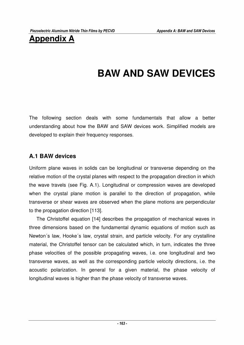
Piezoelectric Aluminum Nitride Thin Films by PECVD Appendix A: BAW and SAW Devices
- 163 -
Appendix A
BAW AND SAW DEVICES
The following section deals with some fundamentals that allow a better
understanding about how the BAW and SAW devices work. Simplified models are
developed to explain their frequency responses.
A.1 BAW devices
Uniform plane waves in solids can be longitudinal or transverse depending on the
relative motion of the crystal planes with respect to the propagation direction in which
the wave travels (see Fig. A.1). Longitudinal or compression waves are developed
when the crystal plane motion is parallel to the direction of propagation, while
transverse or shear waves are observed when the plane motions are perpendicular
to the propagation direction [113].
The Christoffel equation [14] describes the propagation of mechanical waves in
three dimensions based on the fundamental dynamic equations of motion such as
Newton´s law, Hooke´s law, crystal strain, and particle velocity. For any crystalline
material, the Christoffel tensor can be calculated which, in turn, indicates the three
phase velocities of the possible propagating waves, i.e. one longitudinal and two
transverse waves, as well as the corresponding particle velocity directions, i.e. the
acoustic polarization. In general for a given material, the phase velocity of
longitudinal waves is higher than the phase velocity of transverse waves.
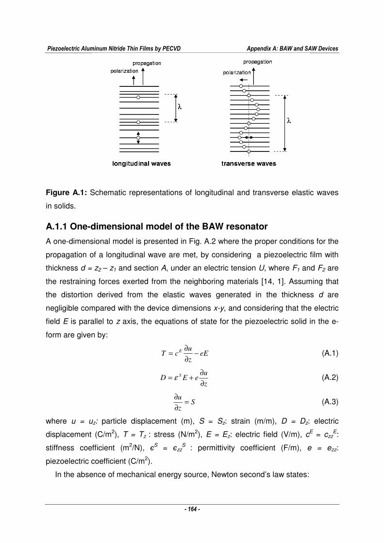
Piezoelectric Aluminum Nitride Thin Films by PECVD Appendix A: BAW and SAW Devices
- 164 -
Figure A.1: Schematic representations of longitudinal and transverse elastic waves
in solids.
A.1.1 One-dimensional model of the BAW resonator
A one-dimensional model is presented in Fig. A.2 where the proper conditions for the
propagation of a longitudinal wave are met, by considering a piezoelectric film with
thickness d = z2 – z1 and section A, under an electric tension U, where F1 and F2 are
the restraining forces exerted from the neighboring materials [14, 1]. Assuming that
the distortion derived from the elastic waves generated in the thickness d are
negligible compared with the device dimensions x-y, and considering that the electric
field E is parallel to z axis, the equations of state for the piezoelectric solid in the e-
form are given by:
eEz
ucT E −
∂
∂= (A.1)
z
ueED S
∂
∂+= ε (A.2)
Sz
u=
∂
∂ (A.3)
where u = uz: particle displacement (m), S = Sz: strain (m/m), D = Dz: electric
displacement (C/m2), T = Tz : stress (N/m2), E = Ez: electric field (V/m), cE = czzE:
stiffness coefficient (m2/N), єS = єzzS : permittivity coefficient (F/m), e = ezz:
piezoelectric coefficient (C/m2).
In the absence of mechanical energy source, Newton second’s law states:
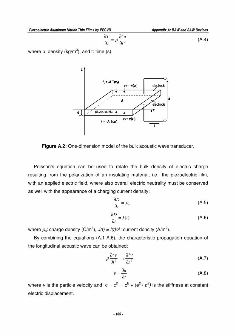
Piezoelectric Aluminum Nitride Thin Films by PECVD Appendix A: BAW and SAW Devices
- 165 -
2
2
t
u
z
T
∂
∂=
∂
∂ρ (A.4)
where ρ: density (kg/m3), and t: time (s).
Figure A.2: One-dimension model of the bulk acoustic wave transducer.
Poisson’s equation can be used to relate the bulk density of electric charge
resulting from the polarization of an insulating material, i.e., the piezoelectric film,
with an applied electric field, where also overall electric neutrality must be conserved
as well with the appearance of a charging current density:
ez
Dρ=
∂
∂ (A.5)
)(tJt
D=
∂
∂ (A.6)
where ρe: charge density (C/m3), J(t) = I(t)/A: current density (A/m2).
By combining the equations (A.1-A.6), the characteristic propagation equation of
the longitudinal acoustic wave can be obtained:
2
2
2
2
zc
t ∂
∂=
∂
∂ ννρ (A.7)
t
u
∂
∂=ν (A.8)
where v is the particle velocity and c = cD = cE + (e2 / єS) is the stiffness at constant
electric displacement.

Piezoelectric Aluminum Nitride Thin Films by PECVD Appendix A: BAW and SAW Devices
- 166 -
The general solution of the propagation equation is the sum of two waves that
travel in opposite directions at a velocity V given by:
ρ
cV = (A.9)
In the harmonic regime the particle velocity is given by,
)(2)(1
)(.)(.kztikzti e
kdtgi
ve
kdtgi
+−
+
= ϖϖν
ν (A.10)
where: ω: angular frequency (radian.s-1), k = ω/V: wavenumber (m-1), v1 = v(z1),
v2 = - v(z2)
By using the stress equations of state:
ϖ
νν
i
hI
kditgkdiZAF ++= )
sin..( 21
1 (A.11)
ϖ
νν
i
hI
tgkdikdiZAF ++= )
.sin.( 21
2 (A.12)
where
Z = ρV = ck/ω: characteristic elastic impedance of the propagation wave (kg.m -2.s),
Z.A: is the elastic impedance (kg/s), h = e/εS : rate between piezoelectric coefficient
(e) and the permittivity (V/m).
The electric tension U applied between the metalized faces can be calculated from
the electric field:
EdzUz
z∫= 2
1 (A.13)
S
D
z
uhE
ε+
∂
∂−= (A.14)
The charging current that flows through the film with section A:
DAiI ϖ= (A.15)
Introducing the particle velocities v1 and v2 and the geometric capacity Co of the
transducer:
)(. 11 zuiϖν = (A.16)
)(. 22 zuiϖν −= (A.17)
d
AC
S
o
ε= (A.18)
Piezoelectric Aluminum Nitride Thin Films by PECVD Appendix A: BAW and SAW Devices
- 167 -
[ ]o
S Ci
Ivv
i
h
Ai
IdzuzuhU
ϖϖϖε++=+−= )()()( 2121 (A.19)
This behavior can be represent by a three-port circuit, with one electrical port –
i.e., applied tension U, and charging injected current I – and two acoustic ports where
the forces F1 and F2 applied on the surface of the film and the input velocities v1 and
v2 mimic the role of tension and current respectively in the electric circuit (see Fig.
A.3).
Figure A.3: The three-port circuit.
If the equations that describe the model are expressed in a matrix form, the
electromechanical impedance matrix is:
−=
IChh
htgkdZAkdZA
hkdZAtgkdZA
i
U
F
F
o
2
1
2
1
/1//
//sin/
/sin//
ν
ν
ϖϖϖ
ϖ
ϖ
(A.20)
Based on the same fundamental considerations equivalent circuit models have
been developed to explain the behavior of the piezoelectric transducer in different
situations [1].
The analysis of the frequency response can be simplified, in a first approach, if the
mechanical effect of the metallic electrodes is discarded because of their
comparatively smaller thickness. However, when the main transducer frequencies
are in the order of the GHz range, the thickness (λ/2) of the film is found to be in the
micrometer range. Under these conditions, the effect of the electrodes must be taken
into account.
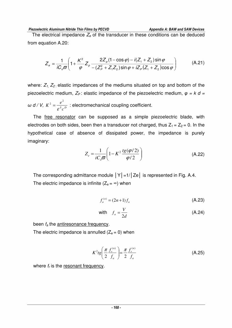
Piezoelectric Aluminum Nitride Thin Films by PECVD Appendix A: BAW and SAW Devices
- 168 -
The electrical impedance Ze of the transducer in these conditions can be deduced
from equation A.20:
( )
+++−
+−−+=
ϕϕ
ϕϕ
ϕϖ cossin)(
sin)()cos1(21
1
21212
212
ZZiZZZZ
ZZiZZ
K
iCZ
PP
p
p
o
e (A.21)
where: Z1, Z2 : elastic impedances of the mediums situated on top and bottom of the
piezoelectric medium, ZP : elastic impedance of the piezoelectric medium, φ = k d =
ω d / V, DS
c
eK
ε
22 = : electromechanical coupling coefficient.
The free resonator can be supposed as a simple piezoelectric blade, with
electrodes on both sides, been then a transducer not charged, thus Z1 = Z2 = 0. In the
hypothetical case of absence of dissipated power, the impedance is purely
imaginary:
−=
2/
)2/(1
1 2
ϕ
ϕ
ϖ
tgK
iCZ
o
e (A.22)
The corresponding admittance module │Y│=1/│Ze│ is represented in Fig. A.4.
The electric impedance is infinite (Ze = ∞) when
a
n
a fnf )12()( += (A.23)
with d
Vf a 2
= (A.24)
been fa the antiresonance frequency.
The electric impedance is annulled (Ze = 0) when
a
n
r
a
n
r
f
f
f
ftgK
)()(2
22
ππ=
(A.25)
where fr is the resonant frequency.
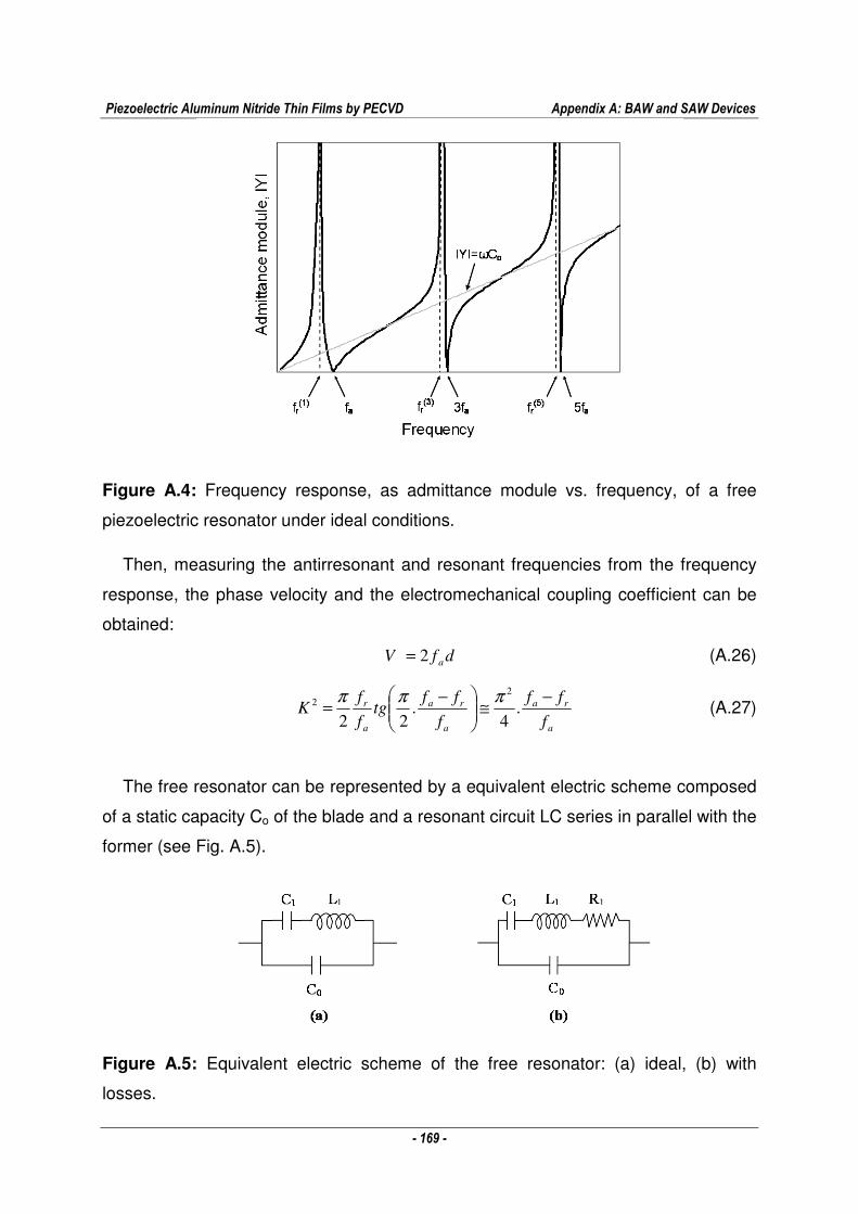
Piezoelectric Aluminum Nitride Thin Films by PECVD Appendix A: BAW and SAW Devices
- 169 -
Figure A.4: Frequency response, as admittance module vs. frequency, of a free
piezoelectric resonator under ideal conditions.
Then, measuring the antirresonant and resonant frequencies from the frequency
response, the phase velocity and the electromechanical coupling coefficient can be
obtained:
dfV a2= (A.26)
a
ra
a
ra
a
r
f
ff
f
fftg
f
fK
−≅
−= .
4.
22
22 πππ
(A.27)
The free resonator can be represented by a equivalent electric scheme composed
of a static capacity Co of the blade and a resonant circuit LC series in parallel with the
former (see Fig. A.5).
Figure A.5: Equivalent electric scheme of the free resonator: (a) ideal, (b) with
losses.
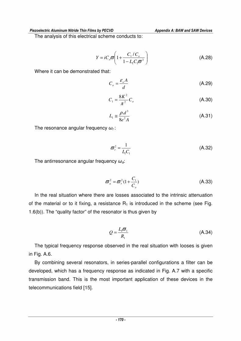
Piezoelectric Aluminum Nitride Thin Films by PECVD Appendix A: BAW and SAW Devices
- 170 -
The analysis of this electrical scheme conducts to:
−+=
211
1
1
/1
ϖϖ
CL
CCiCY o
o (A.28)
Where it can be demonstrated that:
d
AC o
o
ε= (A.29)
oCK
C2
2
1
8
π= (A.30)
Ae
dL
2
3
1 8
.ρ≅ (A.31)
The resonance angular frequency ωr :
11
2 1CL
r =ϖ (A.32)
The antirresonance angular frequency ωa:
)1( 122
o
raC
C+= ϖϖ (A.33)
In the real situation where there are losses associated to the intrinsic attenuation
of the material or to it fixing, a resistance R1 is introduced in the scheme (see Fig.
1.6(b)). The “quality factor” of the resonator is thus given by
1
11
R
LQ
ϖ= (A.34)
The typical frequency response observed in the real situation with looses is given
in Fig. A.6.
By combining several resonators, in series-parallel configurations a filter can be
developed, which has a frequency response as indicated in Fig. A.7 with a specific
transmission band. This is the most important application of these devices in the
telecommunications field [15].
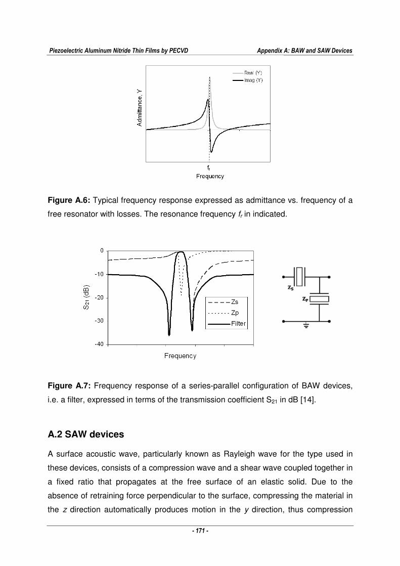
Piezoelectric Aluminum Nitride Thin Films by PECVD Appendix A: BAW and SAW Devices
- 171 -
Figure A.6: Typical frequency response expressed as admittance vs. frequency of a
free resonator with losses. The resonance frequency fr in indicated.
Figure A.7: Frequency response of a series-parallel configuration of BAW devices,
i.e. a filter, expressed in terms of the transmission coefficient S21 in dB [14].
A.2 SAW devices
A surface acoustic wave, particularly known as Rayleigh wave for the type used in
these devices, consists of a compression wave and a shear wave coupled together in
a fixed ratio that propagates at the free surface of an elastic solid. Due to the
absence of retraining force perpendicular to the surface, compressing the material in
the z direction automatically produces motion in the y direction, thus compression
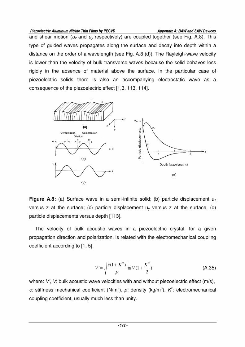
Piezoelectric Aluminum Nitride Thin Films by PECVD Appendix A: BAW and SAW Devices
- 172 -
and shear motion (uz and uy respectively) are coupled together (see Fig. A.8). This
type of guided waves propagates along the surface and decay into depth within a
distance on the order of a wavelength (see Fig. A.8 (d)). The Rayleigh-wave velocity
is lower than the velocity of bulk transverse waves because the solid behaves less
rigidly in the absence of material above the surface. In the particular case of
piezoelectric solids there is also an accompanying electrostatic wave as a
consequence of the piezoelectric effect [1,3, 113, 114].
Figure A.8: (a) Surface wave in a semi-infinite solid; (b) particle displacement uz
versus z at the surface; (c) particle displacement uy versus z at the surface, (d)
particle displacements versus depth [113].
The velocity of bulk acoustic waves in a piezoelectric crystal, for a given
propagation direction and polarization, is related with the electromechanical coupling
coefficient according to [1, 5]:
)2
1()1(
'22
KV
KcV +≅
+=
ρ (A.35)
where: V’, V: bulk acoustic wave velocities with and without piezoelectric effect (m/s),
c: stiffness mechanical coefficient (N/m2), ρ: density (kg/m3), K2: electromechanical
coupling coefficient, usually much less than unity.
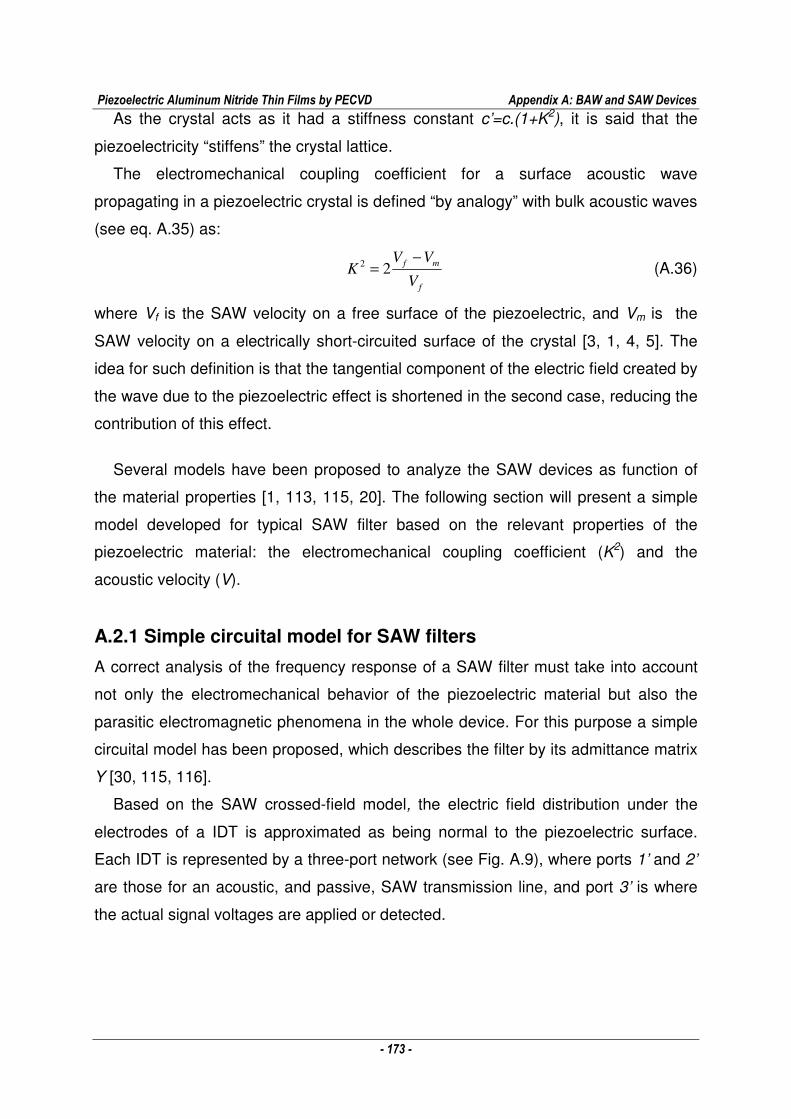
Piezoelectric Aluminum Nitride Thin Films by PECVD Appendix A: BAW and SAW Devices
- 173 -
As the crystal acts as it had a stiffness constant c’=c.(1+K2), it is said that the
piezoelectricity “stiffens” the crystal lattice.
The electromechanical coupling coefficient for a surface acoustic wave
propagating in a piezoelectric crystal is defined “by analogy” with bulk acoustic waves
(see eq. A.35) as:
f
mf
V
VVK
−= 22 (A.36)
where Vf is the SAW velocity on a free surface of the piezoelectric, and Vm is the
SAW velocity on a electrically short-circuited surface of the crystal [3, 1, 4, 5]. The
idea for such definition is that the tangential component of the electric field created by
the wave due to the piezoelectric effect is shortened in the second case, reducing the
contribution of this effect.
Several models have been proposed to analyze the SAW devices as function of
the material properties [1, 113, 115, 20]. The following section will present a simple
model developed for typical SAW filter based on the relevant properties of the
piezoelectric material: the electromechanical coupling coefficient (K2) and the
acoustic velocity (V).
A.2.1 Simple circuital model for SAW filters
A correct analysis of the frequency response of a SAW filter must take into account
not only the electromechanical behavior of the piezoelectric material but also the
parasitic electromagnetic phenomena in the whole device. For this purpose a simple
circuital model has been proposed, which describes the filter by its admittance matrix
Y [30, 115, 116].
Based on the SAW crossed-field model, the electric field distribution under the
electrodes of a IDT is approximated as being normal to the piezoelectric surface.
Each IDT is represented by a three-port network (see Fig. A.9), where ports 1’ and 2’
are those for an acoustic, and passive, SAW transmission line, and port 3’ is where
the actual signal voltages are applied or detected.
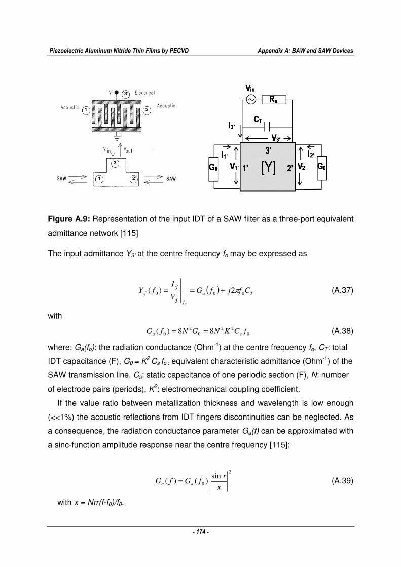
Piezoelectric Aluminum Nitride Thin Films by PECVD Appendix A: BAW and SAW Devices
- 174 -
Figure A.9: Representation of the input IDT of a SAW filter as a three-port equivalent
admittance network [115]
The input admittance Y3’ at the centre frequency fo may be expressed as
( ) Ta
f
CfjfGV
IfY
o
00
3
303
2)('
'
´' π+== (A.37)
with
022
02
0 88)( fCKNGNfG sa == (A.38)
where: Ga(fo): the radiation conductance (Ohm-1) at the centre frequency fo, CT: total
IDT capacitance (F), G0 = K2 Cs fo : equivalent characteristic admittance (Ohm-1) of the
SAW transmission line, Cs: static capacitance of one periodic section (F), N: number
of electrode pairs (periods), K2: electromechanical coupling coefficient.
If the value ratio between metallization thickness and wavelength is low enough
(<<1%) the acoustic reflections from IDT fingers discontinuities can be neglected. As
a consequence, the radiation conductance parameter Ga(f) can be approximated with
a sinc-function amplitude response near the centre frequency [115]:
2
0
sin).()(
x
xfGfG aa = (A.39)
with x = Nπ(f-f0)/f0.
Piezoelectric Aluminum Nitride Thin Films by PECVD Appendix A: BAW and SAW Devices
- 175 -
Then the general expression for the input admittance Y3’:
Ta fCjfGfY π2)()('3+= (A.40)
An expression for the radiation suceptance Ba(f), normally omitted in calculations
because of its magnitude, can be derived from the Ga(f) expression [115]:
−=
20 2
2)2sin().()(
x
xxfGfB aa (A.41)
Based on the same principles, the model can be applied to the output IDT, which
is considered to be excited by a high-impedance current source proportional to the
surface acoustic wave amplitude, and obtain the overall equivalent circuit of the SAW
filter.
In order to obtain the overall SAW filter response, the only concern is with the ratio
of voltages at electrical ports in both input and output IDTs (1 and 2), considered as a
two-port network, as depicted in the block diagram of Fig. A.10. With the aim of
obtaining the admittance parameters, current-voltage relations from standard circuit
theory are used at input and output:
2121111 . VYVYI += (A.42)
2221212 . VYVYI += (A.43)
Figure A.10: Representations of the complete SAW device using three-port electrical
admittances applied to the input and outpout IDTs.
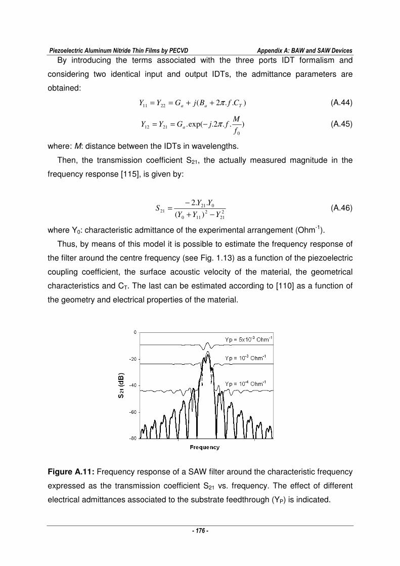
Piezoelectric Aluminum Nitride Thin Films by PECVD Appendix A: BAW and SAW Devices
- 176 -
By introducing the terms associated with the three ports IDT formalism and
considering two identical input and output IDTs, the admittance parameters are
obtained:
)..2(2211 Taa CfBjGYY π++== (A.44)
)..2.exp(.0
2112f
MfjGYY a π−== (A.45)
where: M: distance between the IDTs in wavelengths.
Then, the transmission coefficient S21, the actually measured magnitude in the
frequency response [115], is given by:
221
2110
02121 )(
..2
YYY
YYS
−+
−= (A.46)
where Y0: characteristic admittance of the experimental arrangement (Ohm-1).
Thus, by means of this model it is possible to estimate the frequency response of
the filter around the centre frequency (see Fig. 1.13) as a function of the piezoelectric
coupling coefficient, the surface acoustic velocity of the material, the geometrical
characteristics and CT. The last can be estimated according to [110] as a function of
the geometry and electrical properties of the material.
Figure A.11: Frequency response of a SAW filter around the characteristic frequency
expressed as the transmission coefficient S21 vs. frequency. The effect of different
electrical admittances associated to the substrate feedthrough (YP) is indicated.
Piezoelectric Aluminum Nitride Thin Films by PECVD Appendix A: BAW and SAW Devices
- 177 -
The effects of the electromagnetic feedthrough can be important in the case of
piezoelectric films over low resistivily substrates. In order to take in account this
effect, the addition of a real term YP to the Y12 parameter has been proposed as a
first approximation. This is equivalent to a purely resistive admittance in parallel and
has had good accordance with measurements [115, 116]. Fig A.11 shows the effect
of the electromagnetic feedthrough on the frequency response.
Piezoelectric Aluminum Nitride Thin Films by PECVD Appendix B: Piezoelectric Characterization of Thin Films
- 178 -
Appendix B
PIEZOELECTRIC CHARACTERIZATION
OF THIN FILMS
Piezoelectric properties of thin films can be determined by two main types of
techniques: static or quasi-static measurements and dynamic measurements [19].
While the first group of techniques is typically used for non-resonant applications,
e.g. sensors and actuators, the second group is typical for those applications where
the piezoelectric thin film is used for the generation or detection of high-frequency
bulk acoustic waves (BAW) or surface acoustic waves (SAW).
B.1 Quasi-static measurements
Quasi-static measurements of piezoelectric properties of thin films are based on
either the direct or the converse piezoelectric effect. While in direct measurements
the voltage produced by an applied stress is measured; in the second case the
displacement produced by an applied electric field is obtained through different
methods.
B.1.1 Techniques based on direct piezoelectric effect
If a piezoelectric film of a material with wurtzite-type structure, as AlN, is supposed,
the equation of state 1.14 describes the direct piezoelectric effect.
If stress is applied exclusively in the c-axis direction, without external electric field
(see Fig. B.1(a)), the electric displacement is given by:
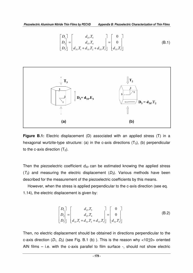
Piezoelectric Aluminum Nitride Thin Films by PECVD Appendix B: Piezoelectric Characterization of Thin Films
- 179 -
(B.1)
Figure B.1: Electric displacement (D) associated with an applied stress (T) in a
hexagonal wurtzite-type structure: (a) in the c-axis directions (T3), (b) perpendicular
to the c-axis direction (T2).
Then the piezoelectric coefficient d33 can be estimated knowing the applied stress
(T3) and measuring the electric displacement (D3). Various methods have been
described for the measurement of the piezoelectric coefficients by this means.
However, when the stress is applied perpendicular to the c-axis direction (see eq.
1.14), the electric displacement is given by:
(B.2)
Then, no electric displacement should be obtained in directions perpendicular to the
c-axis direction (D1, D2) (see Fig. B.1 (b) ). This is the reason why <1010> oriented
AlN films – i.e. with the c-axis parallel to film surface -, should not show electric
=
++
=
333333231131
415
515
3
2
1
.
0
0
...
.
.
TdTdTdTd
Td
Td
D
D
D
=
++
=
231333231131
415
515
3
2
1
.
0
0
...
.
.
TdTdTdTd
Td
Td
D
D
D
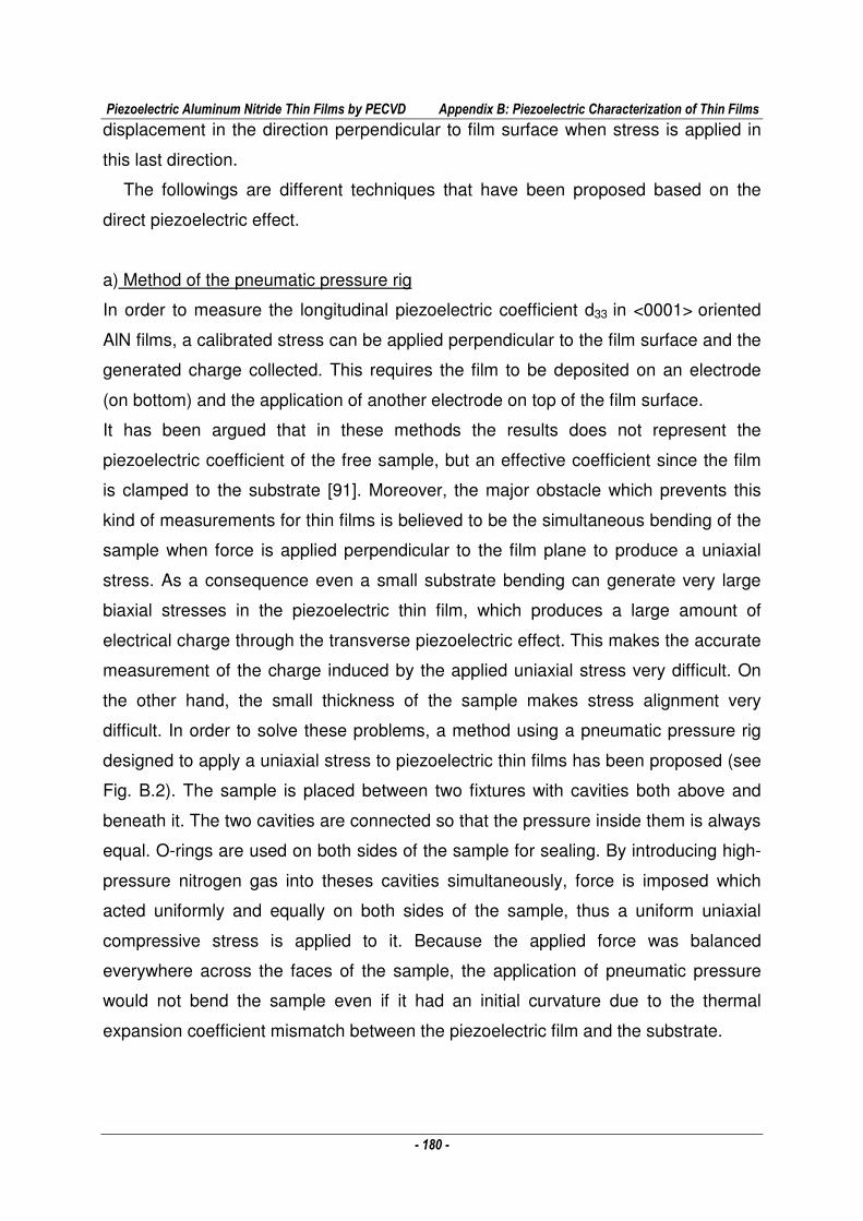
Piezoelectric Aluminum Nitride Thin Films by PECVD Appendix B: Piezoelectric Characterization of Thin Films
- 180 -
displacement in the direction perpendicular to film surface when stress is applied in
this last direction.
The followings are different techniques that have been proposed based on the
direct piezoelectric effect.
a) Method of the pneumatic pressure rig
In order to measure the longitudinal piezoelectric coefficient d33 in <0001> oriented
AlN films, a calibrated stress can be applied perpendicular to the film surface and the
generated charge collected. This requires the film to be deposited on an electrode
(on bottom) and the application of another electrode on top of the film surface.
It has been argued that in these methods the results does not represent the
piezoelectric coefficient of the free sample, but an effective coefficient since the film
is clamped to the substrate [91]. Moreover, the major obstacle which prevents this
kind of measurements for thin films is believed to be the simultaneous bending of the
sample when force is applied perpendicular to the film plane to produce a uniaxial
stress. As a consequence even a small substrate bending can generate very large
biaxial stresses in the piezoelectric thin film, which produces a large amount of
electrical charge through the transverse piezoelectric effect. This makes the accurate
measurement of the charge induced by the applied uniaxial stress very difficult. On
the other hand, the small thickness of the sample makes stress alignment very
difficult. In order to solve these problems, a method using a pneumatic pressure rig
designed to apply a uniaxial stress to piezoelectric thin films has been proposed (see
Fig. B.2). The sample is placed between two fixtures with cavities both above and
beneath it. The two cavities are connected so that the pressure inside them is always
equal. O-rings are used on both sides of the sample for sealing. By introducing high-
pressure nitrogen gas into theses cavities simultaneously, force is imposed which
acted uniformly and equally on both sides of the sample, thus a uniform uniaxial
compressive stress is applied to it. Because the applied force was balanced
everywhere across the faces of the sample, the application of pneumatic pressure
would not bend the sample even if it had an initial curvature due to the thermal
expansion coefficient mismatch between the piezoelectric film and the substrate.
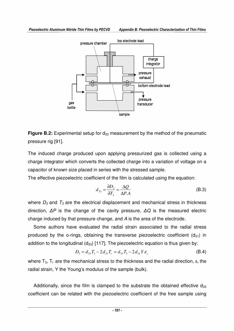
Piezoelectric Aluminum Nitride Thin Films by PECVD Appendix B: Piezoelectric Characterization of Thin Films
- 181 -
Figure B.2: Experimental setup for d33 measurement by the method of the pneumatic
pressure rig [91].
The induced charge produced upon applying pressurized gas is collected using a
charge integrator which converts the collected charge into a variation of voltage on a
capacitor of known size placed in series with the stressed sample.
The effective piezoelectric coefficient of the film is calculated using the equation:
AP
Q
T
Dd
.3
333
∆
∆=
∂
∂= (B.3)
where D3 and T3 are the electrical displacement and mechanical stress in thickness
direction, ∆P is the change of the cavity pressure, ∆Q is the measured electric
charge induced by that pressure change, and A is the area of the electrode.
Some authors have evaluated the radial strain associated to the radial stress
produced by the o-rings, obtaining the transverse piezoelectric coefficient (d31) in
addition to the longitudinal (d33) [117]. The piezoelectric equation is thus given by:
rr YdTdTdTdD ε31333313333 22 −=−= (B.4)
where T3, Tr are the mechanical stress to the thickness and the radial direction, εr the
radial strain, Y the Young’s modulus of the sample (bulk).
Additionally, since the film is clamped to the substrate the obtained effective d33
coefficient can be related with the piezoelectric coefficient of the free sample using
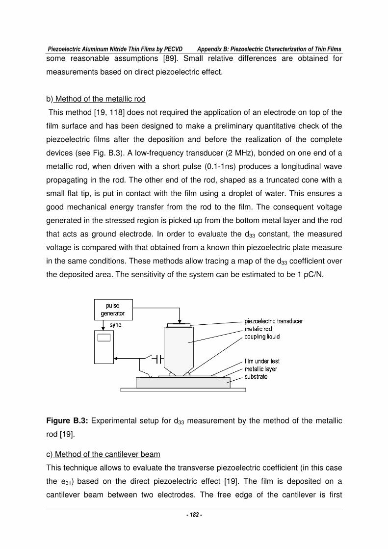
Piezoelectric Aluminum Nitride Thin Films by PECVD Appendix B: Piezoelectric Characterization of Thin Films
- 182 -
some reasonable assumptions [89]. Small relative differences are obtained for
measurements based on direct piezoelectric effect.
b) Method of the metallic rod
This method [19, 118] does not required the application of an electrode on top of the
film surface and has been designed to make a preliminary quantitative check of the
piezoelectric films after the deposition and before the realization of the complete
devices (see Fig. B.3). A low-frequency transducer (2 MHz), bonded on one end of a
metallic rod, when driven with a short pulse (0.1-1ns) produces a longitudinal wave
propagating in the rod. The other end of the rod, shaped as a truncated cone with a
small flat tip, is put in contact with the film using a droplet of water. This ensures a
good mechanical energy transfer from the rod to the film. The consequent voltage
generated in the stressed region is picked up from the bottom metal layer and the rod
that acts as ground electrode. In order to evaluate the d33 constant, the measured
voltage is compared with that obtained from a known thin piezoelectric plate measure
in the same conditions. These methods allow tracing a map of the d33 coefficient over
the deposited area. The sensitivity of the system can be estimated to be 1 pC/N.
Figure B.3: Experimental setup for d33 measurement by the method of the metallic
rod [19].
c) Method of the cantilever beam
This technique allows to evaluate the transverse piezoelectric coefficient (in this case
the e31) based on the direct piezoelectric effect [19]. The film is deposited on a
cantilever beam between two electrodes. The free edge of the cantilever is first
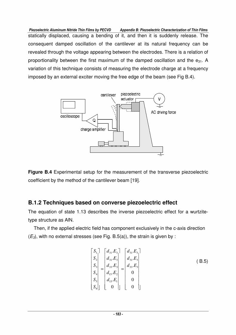
Piezoelectric Aluminum Nitride Thin Films by PECVD Appendix B: Piezoelectric Characterization of Thin Films
- 183 -
statically displaced, causing a bending of it, and then it is suddenly release. The
consequent damped oscillation of the cantilever at its natural frequency can be
revealed through the voltage appearing between the electrodes. There is a relation of
proportionality between the first maximum of the damped oscillation and the e31. A
variation of this technique consists of measuring the electrode charge at a frequency
imposed by an external exciter moving the free edge of the beam (see Fig B.4).
Figure B.4 Experimental setup for the measurement of the transverse piezoelectric
coefficient by the method of the cantilever beam [19].
B.1.2 Techniques based on converse piezoelectric effect
The equation of state 1.13 describes the inverse piezoelectric effect for a wurtzite-
type structure as AlN.
Then, if the applied electric field has component exclusively in the c-axis direction
(E3), with no external stresses (see Fig. B.5(a)), the strain is given by :
( B.5)
=
=
0
0
0
.
.
.
0
.
.
.
.
.
333
331
331
115
215
333
331
331
6
5
4
3
2
1
Ed
Ed
Ed
Ed
Ed
Ed
Ed
Ed
S
S
S
S
S
S
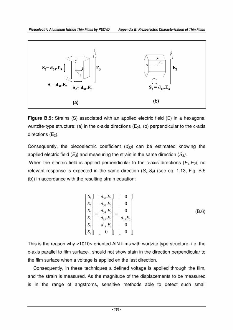
Piezoelectric Aluminum Nitride Thin Films by PECVD Appendix B: Piezoelectric Characterization of Thin Films
- 184 -
Figure B.5: Strains (S) associated with an applied electric field (E) in a hexagonal
wurtzite-type structure: (a) in the c-axis directions (E3), (b) perpendicular to the c-axis
directions (E2).
Consequently, the piezoelectric coefficient (d33) can be estimated knowing the
applied electric field (E3) and measuring the strain in the same direction (S3).
When the electric field is applied perpendicular to the c-axis directions (E1,E2), no
relevant response is expected in the same direction (S1,S2) (see eq. 1.13, Fig. B.5
(b)) in accordance with the resulting strain equation:
(B.6)
This is the reason why <1010> oriented AlN films with wurtzite type structure- i.e. the
c-axis parallel to film surface-, should not show stain in the direction perpendicular to
the film surface when a voltage is applied en the last direction.
Consequently, in these techniques a defined voltage is applied through the film,
and the strain is measured. As the magnitude of the displacements to be measured
is in the range of angstroms, sensitive methods able to detect such small
=
=
0
0
0
0
0
0
.
.
.
.
.
215
115
215
333
331
331
6
5
4
3
2
1
Ed
Ed
Ed
Ed
Ed
Ed
S
S
S
S
S
S
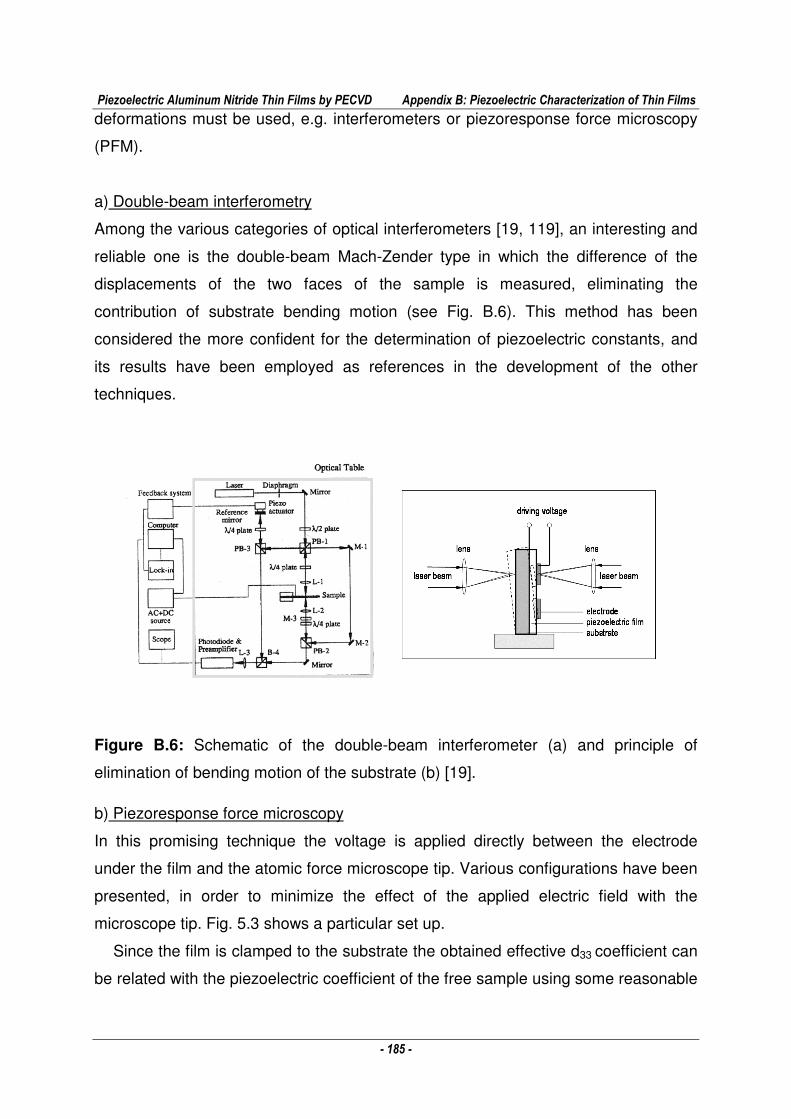
Piezoelectric Aluminum Nitride Thin Films by PECVD Appendix B: Piezoelectric Characterization of Thin Films
- 185 -
deformations must be used, e.g. interferometers or piezoresponse force microscopy
(PFM).
a) Double-beam interferometry
Among the various categories of optical interferometers [19, 119], an interesting and
reliable one is the double-beam Mach-Zender type in which the difference of the
displacements of the two faces of the sample is measured, eliminating the
contribution of substrate bending motion (see Fig. B.6). This method has been
considered the more confident for the determination of piezoelectric constants, and
its results have been employed as references in the development of the other
techniques.
Figure B.6: Schematic of the double-beam interferometer (a) and principle of
elimination of bending motion of the substrate (b) [19].
b) Piezoresponse force microscopy
In this promising technique the voltage is applied directly between the electrode
under the film and the atomic force microscope tip. Various configurations have been
presented, in order to minimize the effect of the applied electric field with the
microscope tip. Fig. 5.3 shows a particular set up.
Since the film is clamped to the substrate the obtained effective d33 coefficient can
be related with the piezoelectric coefficient of the free sample using some reasonable
Piezoelectric Aluminum Nitride Thin Films by PECVD Appendix B: Piezoelectric Characterization of Thin Films
- 186 -
assumptions [89]. Significant relative differences are obtained for measurements
based on inverse piezoelectric effect (see section 5.2.4.1).
B.2 Dynamic measurements
These methods are based on the evaluation of the performance of BAW or SAW
devices constructed with the piezoelectric films. As these applications are of main
interest, they are of great importance.
Typically, the frequency response of the device is measured using a Network
Analyzer. Based on this, the electromechanical coupling coefficient, acoustic velocity
and other parameters can be estimate using the appropriate model for the response
(see Appendix A) [24, 8].
In the particular case of SAW devices, the determination of the characteristic
frequency with the surface between the IDTs metalized and non-moralized, allows for
the estimation of the electromechanical coupling coefficient in accordance with its
definition (see Appendix A) [13, 8]. Additionally, models of the frequency response
can be used to obtain the relevant parameters.
Piezoelectric Aluminum Nitride Thin Films by PECVD Appendix C: The Electric Field Under the Electrodes
- 187 -
Appendix C
A MODEL OF THE ELECTRIC FIELD
UNDER THE ELECTRODES
The electric field distribution under the IDTs of SAW devices was consider relevant in
order to explain the frequency response obtained for devices based on different AlN
films. Therefore, the finite differences method was used to solve the differential
equations that describe this phenomenon, under different configurations of interest.
C.1 The problem
The basic configuration of interdigital electrodes that compose the SAW device are
supposed as shown in Fig. A.18. The rate value electrode size to distance between
electrodes is fixed in accordance with the used geometry. The electrodes are placed
on the surface of a dielectric film with variable thickness, i.e. the AlN film, which is
deposited over an electrical conductive substrate. Adjacent electrodes are
considered with opposite electrical potential in a given moment. Then, the object of
the problem is to find the electric potential distribution and consequent electric field
distribution in the film profile. Since, the length of the electrodes is substantially
higher than the other dimensions – i.e. electrode width, distance between electrodes
or film thickness - , a two dimensional analysis in the x-z plane can be done to solve
the problem. Additionally, the symmetry elements allow restricting the analysis to the
indicated portion of the profile (see Fig. C.1).
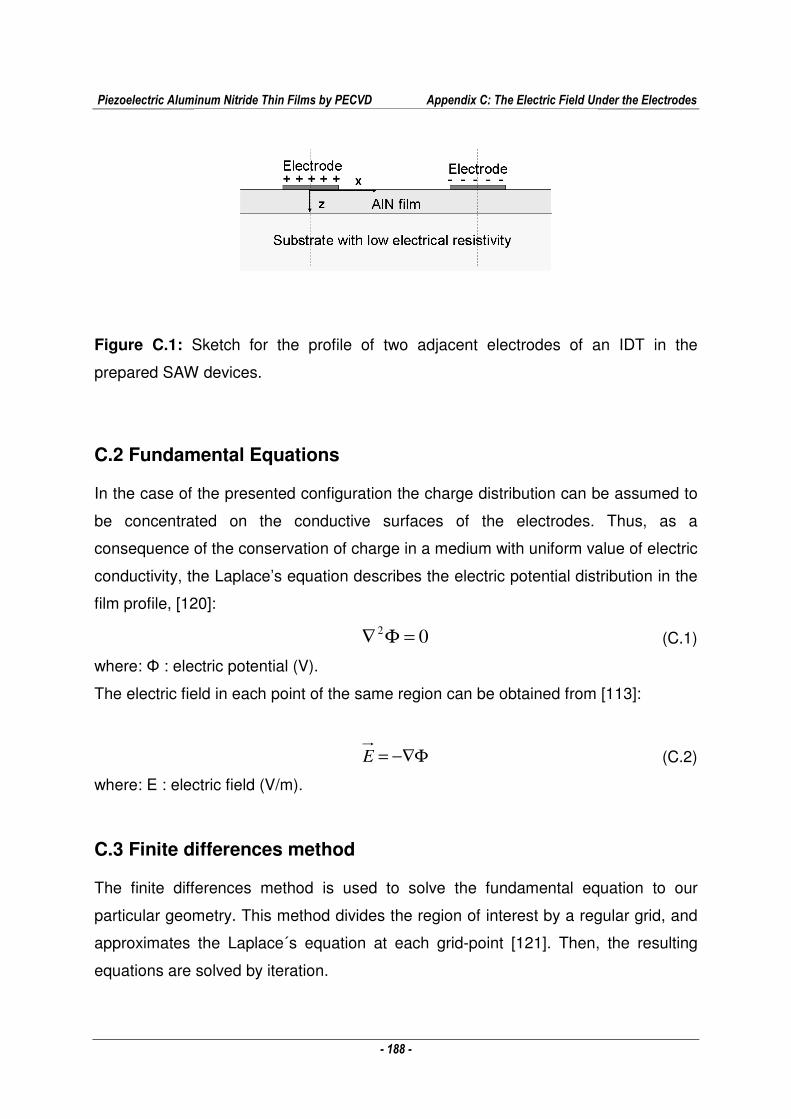
Piezoelectric Aluminum Nitride Thin Films by PECVD Appendix C: The Electric Field Under the Electrodes
- 188 -
Figure C.1: Sketch for the profile of two adjacent electrodes of an IDT in the
prepared SAW devices.
C.2 Fundamental Equations
In the case of the presented configuration the charge distribution can be assumed to
be concentrated on the conductive surfaces of the electrodes. Thus, as a
consequence of the conservation of charge in a medium with uniform value of electric
conductivity, the Laplace’s equation describes the electric potential distribution in the
film profile, [120]:
02 =Φ∇ (C.1)
where: Φ : electric potential (V).
The electric field in each point of the same region can be obtained from [113]:
Φ−∇=E (C.2)
where: E : electric field (V/m).
C.3 Finite differences method
The finite differences method is used to solve the fundamental equation to our
particular geometry. This method divides the region of interest by a regular grid, and
approximates the Laplace´s equation at each grid-point [121]. Then, the resulting
equations are solved by iteration.
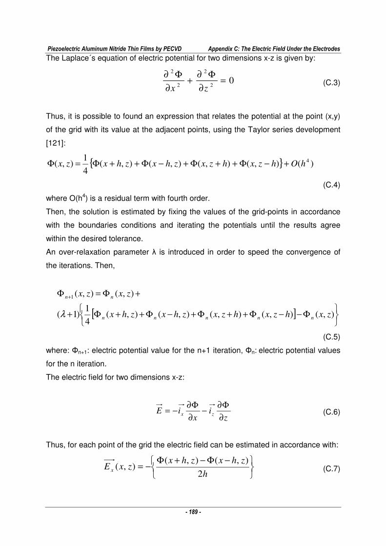
Piezoelectric Aluminum Nitride Thin Films by PECVD Appendix C: The Electric Field Under the Electrodes
- 189 -
The Laplace´s equation of electric potential for two dimensions x-z is given by:
02
2
2
2
=∂
Φ∂+
∂
Φ∂
zx (C.3)
Thus, it is possible to found an expression that relates the potential at the point (x,y)
of the grid with its value at the adjacent points, using the Taylor series development
[121]:
{ } )(),(),(),(),(4
1),( 4hOhzxhzxzhxzhxzx +−Φ++Φ+−Φ++Φ=Φ
(C.4)
where O(h4) is a residual term with fourth order.
Then, the solution is estimated by fixing the values of the grid-points in accordance
with the boundaries conditions and iterating the potentials until the results agree
within the desired tolerance.
An over-relaxation parameter λ is introduced in order to speed the convergence of
the iterations. Then,
[ ]
Φ−−Φ++Φ+−Φ++Φ+
+Φ=Φ +
),(),(),(),(),(4
1)1(
),(),(1
zxhzxhzxzhxzhx
zxzx
nnnnn
nn
λ
(C.5)
where: Φn+1: electric potential value for the n+1 iteration, Φn: electric potential values
for the n iteration.
The electric field for two dimensions x-z:
zi
xiE zx
∂
Φ∂−
∂
Φ∂−= (C.6)
Thus, for each point of the grid the electric field can be estimated in accordance with:
−Φ−+Φ
−=h
zhxzhxzxE x 2
),(),(),( (C.7)
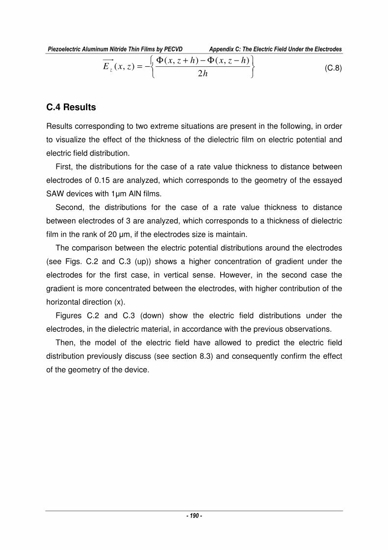
Piezoelectric Aluminum Nitride Thin Films by PECVD Appendix C: The Electric Field Under the Electrodes
- 190 -
−Φ−+Φ
−=h
hzxhzxzxE z 2
),(),(),( (C.8)
C.4 Results
Results corresponding to two extreme situations are present in the following, in order
to visualize the effect of the thickness of the dielectric film on electric potential and
electric field distribution.
First, the distributions for the case of a rate value thickness to distance between
electrodes of 0.15 are analyzed, which corresponds to the geometry of the essayed
SAW devices with 1µm AlN films.
Second, the distributions for the case of a rate value thickness to distance
between electrodes of 3 are analyzed, which corresponds to a thickness of dielectric
film in the rank of 20 µm, if the electrodes size is maintain.
The comparison between the electric potential distributions around the electrodes
(see Figs. C.2 and C.3 (up)) shows a higher concentration of gradient under the
electrodes for the first case, in vertical sense. However, in the second case the
gradient is more concentrated between the electrodes, with higher contribution of the
horizontal direction (x).
Figures C.2 and C.3 (down) show the electric field distributions under the
electrodes, in the dielectric material, in accordance with the previous observations.
Then, the model of the electric field have allowed to predict the electric field
distribution previously discuss (see section 8.3) and consequently confirm the effect
of the geometry of the device.
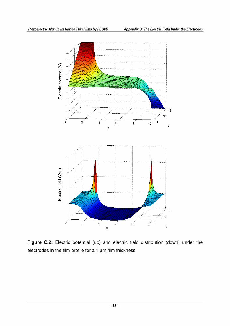
Piezoelectric Aluminum Nitride Thin Films by PECVD Appendix C: The Electric Field Under the Electrodes
- 191 -
Figure C.2: Electric potential (up) and electric field distribution (down) under the
electrodes in the film profile for a 1 µm film thickness.
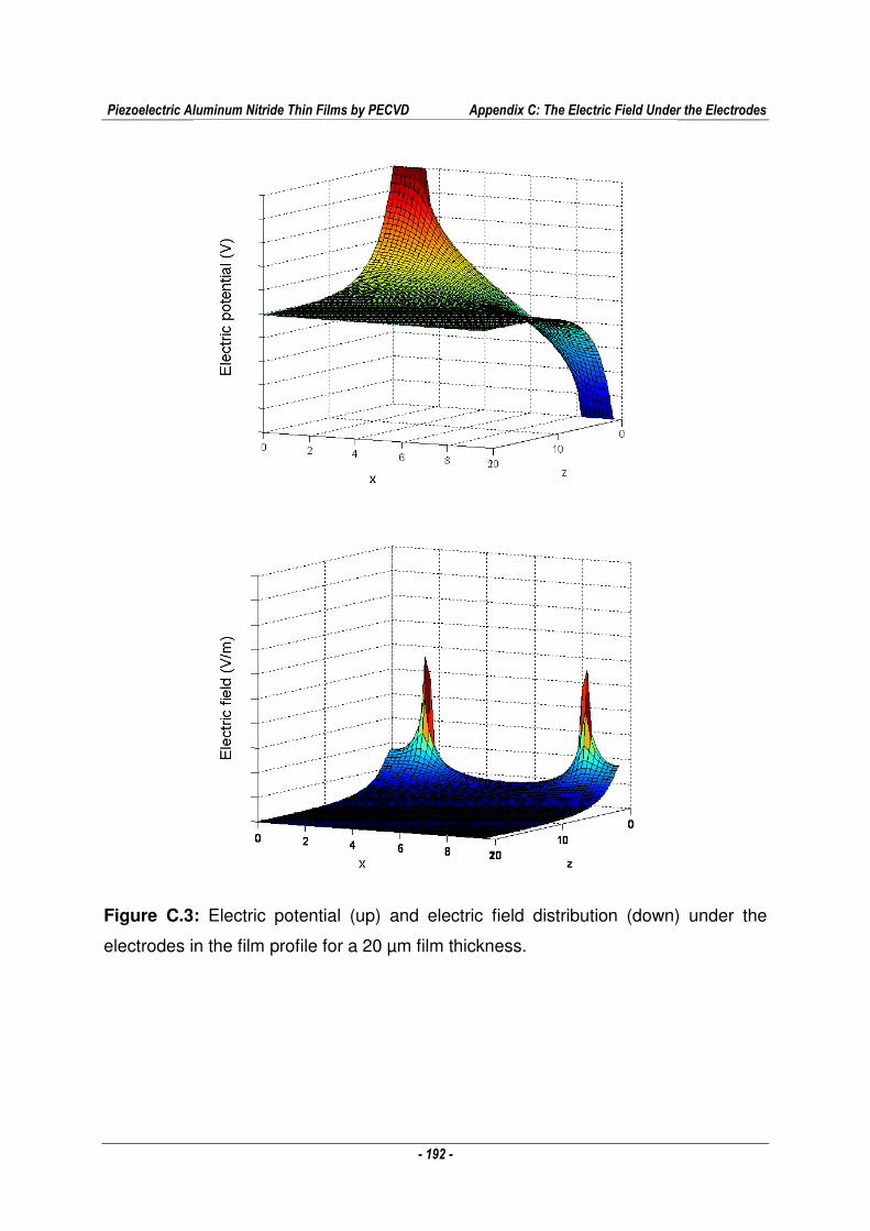
Piezoelectric Aluminum Nitride Thin Films by PECVD Appendix C: The Electric Field Under the Electrodes
- 192 -
Figure C.3: Electric potential (up) and electric field distribution (down) under the
electrodes in the film profile for a 20 µm film thickness.
Piezoelectric Aluminum Nitride Thin Films by PECVD Resumen ejecutivo
- 193 -
Resumen ejecutivo
PELÍCULAS DELGADAS PIEZOELECTRICAS
DE NITRURO DE ALUMINIO POR PECVD
Un sólido es piezoeléctrico si se polariza eléctricamente bajo la acción de una fuerza
mecánica (efecto directo), y se deforma mecánicamente cuando se aplica un campo
eléctrico sobre él (efecto inverso). El origen de este fenómeno está en la estructura
cristalina del sólido, y particularmente en la simetría de la misma. La distribución de
densidad electrónica no uniforme en los enlaces entre los átomos genera un arreglo
periódico de dipolos en la red cristalina. Cuando se aplica una fuerza, la deformación
generada en el cristal crea cambios en los largos y direcciones de los enlaces entre
los átomos de la red. Como consecuencia, se producen cambios en las magnitudes
y direcciones de los dipolos individuales. Este hecho puede conducir a una
polarización neta de la red cristalina, dando lugar al efecto piezoeléctrico. Como
consecuencia, este efecto está presente en 20 de las 21 estructuras cristalinas no-
centro-simétricas. Dado que la piezoelectricidad implica un acoplamiento lineal entre
los sistemas mecánico y eléctrico, las ecuaciones de estado que describen el
fenómeno se pueden representar como:
ii
EEdTsS .. αβαβα += (1)
j
T
ijii ETdD .. εαα += (2)
con i, ,j = 1, 2, 3 y α, β = 1, 2, …6; siendo S : deformación (m/m), D :
desplazamiento eléctrico (C/m2), T : tensión (N/m2), E : campo eléctrico (V/m), sE :
constante elástica (m2/N), єT : constante dieléctrica (F/m) y d : constante
piezoeléctrica (m/V).
Piezoelectric Aluminum Nitride Thin Films by PECVD Resumen ejecutivo
- 194 -
Como consecuencia del empleo generalizado de las energías mecánica y
eléctrica en la vida cotidiana, los materiales piezoeléctricos ofrecen un gran potencial
en el desarrollo de dispositivos para numerosas aplicaciones. Los dispositivos
electroacústicos basados en materiales piezoeléctricos -ampliamente empleados
como osciladores, sensores, y resonadores- presentan actualmente su mayor
demanda en la industria de las telecomunicaciones. En el sector de las
comunicaciones inalámbricas, existe un importante consumo de filtros para el control
de la frecuencia de operación del dispositivo en cuestión, normalmente componentes
del tipo “surface acoustic wave” (SAW) y “bulk acoustic wave” (BAW). La frecuencia
característica de operación de los mismos (f, en s-1) es la dada por la expresión:
d
VVf
20
==λ
(3)
donde: V es la velocidad de onda acústica en el material (m/s), λ0 la longitud de
onda (m) y d la dimensión característica del dispositivo.
El marcado crecimiento de los sistemas de comunicación ha generado la
necesidad de emplear frecuencias cada vez más elevadas hasta, actualmente, el
rango de los GHz, v.g. microondas. El aumento de la frecuencia (f) de operación del
dispositivo se consigue, para un dado material, reduciendo sus dimensiones (d).
Esto se ha logrado a costos razonables mediante el empleo de películas
delgadas piezoeléctricas, para las cuales las técnicas de obtención adecuadas abren
la posibilidad de unificar las tecnologías de circuitos integrados y de dispositivos
electro-acústicos.
Las características buscadas en un material adecuado para la fabricación de
películas delgadas piezoeléctricas para estas aplicaciones son: alto acoplamiento
piezoeléctrico, alta velocidad de onda acústica, estabilidad térmica, y baja rugosidad
superficial.
El nitruro de aluminio es un material piezoeléctrico debido a su estructura
cristalina hexagonal tipo wurtzita, y al mismo tiempo presenta una velocidad de onda
acústica particularmente elevada debido a sus excelente propiedades mecánicas.
Además de poseer una excelente estabilidad térmica, se caracteriza por su alta
conductividad térmica, y un elevado “band gap”, de 6,2 eV siendo un excelente
aislante eléctrico cuando se encuentra puro y el compuesto es estequiométrico.
Piezoelectric Aluminum Nitride Thin Films by PECVD Resumen ejecutivo
- 195 -
El desempeño de las películas delgadas de nitruro de aluminio para aplicaciones
piezoeléctricas está directamente relacionado con la microestructura y composición
de las mismas. Aunque en la situación ideal sería deseable emplear películas
monocristalinas para estas aplicaciones, las películas policristalinas con orientación
preferencial respecto al plano del sustrato tienen un desempeño excelente siendo su
producción mucho más sencilla y económica.
Los dispositivos BAW se basan en la generación de ondas acústicas
longitudinales perpendiculares a la película. Como consecuencia, filmes delgados
orientados en la dirección <0001>, con el eje c perpendicular a la superficie del
sustrato, son los preferidos de manera de optimizar el acoplamiento piezoeléctrico.
Para los dispositivos SAW, basados en ondas acústicas de superficie, se emplean
filmes con la misma orientación, aunque se ha sugerido la conveniencia de utilizar
también la orientación <1010> con el eje c paralelo a la superficie del sustrato.
El grado de orientación de las películas delgadas policristalinas de AlN constituye
un parámetro importante de la microestructura ya que está directamente relacionado
con el desempeño piezoeléctrico del componente fabricado. La configuración Bragg-
Brentano θ/2θ, tradicionalmente empleada en el análisis por difracción de rayos X
(DRX), muestra en el difractograma las reflexiones correspondientes a los planos
paralelos al sustrato, constituyendo así una primera indicación de la orientación
preferencial del la película. Pueden emplearse también otras técnicas para obtener
una medida más fina de la dispersión en la orientación de la película respecto a la
dirección de referencia, para las cuales el ancho a la altura media (FWHM) de la
curva obtenida es una medida directa del la dispersión en la orientación
normalmente empleada como referencia. Aunque en general se ha relacionado este
último parámetro con el desempeño piezoeléctrico, estudios recientes han sugerido
que esa correlación no existe en todos los casos. La razón de esta ausencia de
correlación es asignada a la presencia granos con polaridades cristalográficas
opuestas, denominados dominios de inversión, indistinguibles mediante DRX, y
difíciles de identificar por otros medios.
Varias técnicas han sido empleadas para obtener películas delgadas de AlN,
como MBE (Molecular Beam Epitaxy), MOCVD (Metal-Organic Chemical Vapor
Deposition), o PVD (Physical Vapor Deposition) obteniéndose en cada caso
diferentes tipos de microestructuras, desde monocristalinas a policristalinas e incluso
Piezoelectric Aluminum Nitride Thin Films by PECVD Resumen ejecutivo
- 196 -
amorfas. La obtención de películas monocristalinas implica elevadas temperaturas o
tiempos de deposición incompatibles con los objetivos económicos necesarios para
la fabricación de dispositivos de uso masivo.
Entre las técnicas disponibles para la obtención de filmes policristalinos, las que
emplean un plasma, v.g. las “asistidas por plasma”, son particularmente importantes
ya que permiten reducir la temperatura de procesamiento. Teniendo en cuenta que
un plasma es un gas quasi-neutro compuesto de electrones libres, iones y especies
neutras que exhibe un comportamiento colectivo, los plasmas de baja densidad
poseen la propiedad particular de presentar las diferentes especies en equilibrio
térmico independiente. Como consecuencia, los electrones y las especies pesadas
presetan temperaturas asociadas muy diferentes. Este tipo de plasma proporciona la
energía de activación para las reacciones químicas a través de colisiones inelásticas
de los electrones libres de alta energía con las especies reaccionantes, manteniendo
simultáneamente una temperatura de sustrato relativamente baja. Adicionalmente se
pueden generar efectos sobre la microestructura de las películas controlando el
bombardeo de iones positivos sobre la película antes y durante la deposición.
Dentro de las técnicas asistidas por plasma se encuentran las PVD (Physical
Vapor Deposition) asociadas con la transferencia de material desde un material
blanco (target) por evaporación o “sputtering”, y las CVD (Chemical Vapor
Deposition) que involucran el ingreso de compuestos volátiles químicamente
reactivos a la cámara de reacción. Las técnicas PECVD (Plasma Enhanced
Chemical Vapor Deposition), y en particular las que emplean excitación por
microondas para generar el plasma, ofrecen numerosas ventajas: a) disponibilidad
de diversos parámetros a ajustar para alcanzar la optimización de las propiedades
de las películas, b) posibilidad de minimizar los efectos de contaminación debido a la
ausencia de un electrodo en la cámara de reacción, c) posibilidad de deposición
sobre sustratos con geometrías más complejas, al ser procesos de deposición
menos direccionales que los de “sputtering”.
A pesar de las ventajas enumeradas, la técnica PECVD con excitación por
microondas no ha sido muy empleada, y tampoco se ha informado la capacidad de
controlar la orientación del film, como <0001> o <1010>, cuando esta técnica ha sido
empleada. Como consecuencia, el objetivo del presente trabajo es la determinación
del efecto de las diferentes variables del proceso con el fin de obtener películas
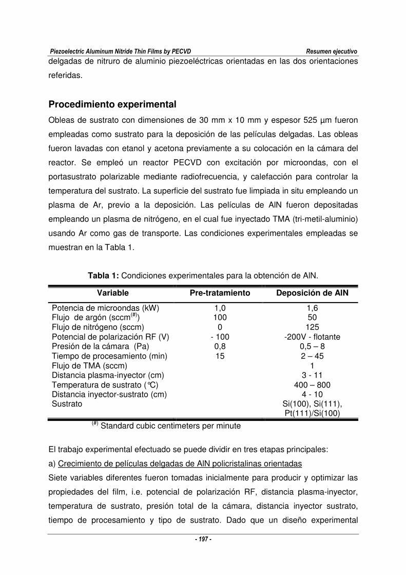
Piezoelectric Aluminum Nitride Thin Films by PECVD Resumen ejecutivo
- 197 -
delgadas de nitruro de aluminio piezoeléctricas orientadas en las dos orientaciones
referidas.
Procedimiento experimental
Obleas de sustrato con dimensiones de 30 mm x 10 mm y espesor 525 µm fueron
empleadas como sustrato para la deposición de las películas delgadas. Las obleas
fueron lavadas con etanol y acetona previamente a su colocación en la cámara del
reactor. Se empleó un reactor PECVD con excitación por microondas, con el
portasustrato polarizable mediante radiofrecuencia, y calefacción para controlar la
temperatura del sustrato. La superficie del sustrato fue limpiada in situ empleando un
plasma de Ar, previo a la deposición. Las películas de AlN fueron depositadas
empleando un plasma de nitrógeno, en el cual fue inyectado TMA (tri-metil-aluminio)
usando Ar como gas de transporte. Las condiciones experimentales empleadas se
muestran en la Tabla 1.
Tabla 1: Condiciones experimentales para la obtención de AlN.
Variable Pre-tratamiento Deposición de AlN
Potencia de microondas (kW) 1,0 1,6 Flujo de argón (sccm(#)) 100 50 Flujo de nitrógeno (sccm) 0 125 Potencial de polarización RF (V) - 100 -200V - flotante Presión de la cámara (Pa) 0,8 0,5 – 8 Tiempo de procesamiento (min) 15 2 – 45 Flujo de TMA (sccm) 1 Distancia plasma-inyector (cm) 3 - 11 Temperatura de sustrato (°C) 400 – 800 Distancia inyector-sustrato (cm) 4 - 10 Sustrato Si(100), Si(111),
Pt(111)/Si(100)
(#) Standard cubic centimeters per minute
El trabajo experimental efectuado se puede dividir en tres etapas principales:
a) Crecimiento de películas delgadas de AlN policristalinas orientadas
Siete variables diferentes fueron tomadas inicialmente para producir y optimizar las
propiedades del film, i.e. potencial de polarización RF, distancia plasma-inyector,
temperatura de sustrato, presión total de la cámara, distancia inyector sustrato,
tiempo de procesamiento y tipo de sustrato. Dado que un diseño experimental
Piezoelectric Aluminum Nitride Thin Films by PECVD Resumen ejecutivo
- 198 -
completo resultaba excesivo para verificar el efecto de todas las variables y sus
interacciones, se efectuó un trabajo preliminar para conocer la influencia de la
distancia plasma-inyector y potencial de polarización RF. Luego que los valores
adecuados de estas dos variables fueron escogidos, el resto de las variables fueron
exploradas usando varios niveles en cada caso.
b) Optimización de las propiedades de las películas
Se efectuaron corridas experimentales adicionales para optimizar el desempeño de
las películas en aplicaciones electroacústicas, tomando los resultados anteriores
como referencia. Se efectuó un diseño experimental completo para temperatura de
sustrato y presión total con el fin de optimizar el desarrollo de las películas
orientadas <1010>. El espesor de las películas y el potencial de polarización fueron
explorados separadamente empleando varios niveles en cada caso con el fin de
optimizar el desarrollo de películas orientadas <0001>. Una caracterización más fina
de la microestructura de las películas, así como la medida de su desempeño
piezoeléctrico, fueron efectuadas en esta etapa. Esto fue complementado por la
caracterización del plasma de proceso en diferentes condiciones de deposición
mediante epectroscopia óptica de emisión (OES).
c) Aplicación dispositivos electroacústicos
Dispositivos electroacústicos tipo SAW fueron preparados empleando películas
delgadas de AlN orientadas <0001> y <1010> en condiciones óptimas, así como
dispositivos electroacústicos tipo BAW con películas orientadas <0001>. La
respuesta de frecuencia de estos dispositivos fue medida y se emplearon modelos
para explicar los resultados obtenidos en cada caso.
Los diagramas Ө/2Ө de difracción de rayos X (DRX) fueron obtenidos entre 15° y
80° (2Ө). Se obtuvieron medidas de la dispersión de las orientaciones para los filmes
mono-orientados, v.g. “rocking curves”, y sus anchos a la altura media (FWHM)
fueron estimados para evaluar el grado de orientación.
Se empleó espectroscopía infrarroja con transformada de Fourier (IRTF), en modo
transmisión entre 4000 cm-1 y 400 cm-1, usando el espectro del sustrato de Si como
referencia y en modo de reflexión.
La morfología superficial de las películas fue analizada por microscopía de fuerza
atómica (AFM). El coeficiente de rugosidad Sa, i.e. la media aritmética del valor
absoluto de la rugosidad superficial, fue determinado por AFM.
Piezoelectric Aluminum Nitride Thin Films by PECVD Resumen ejecutivo
- 199 -
Las muestras producidas y sus superficies de fractura fueron observadas por
microscopía electrónicas de barrido (MEB). Se empleó microscopía electrónica de
transmisión del alta resolución y SAED para un estudio fino de la microestructura del
perfil de las películas.
Se analizó la composición de las películas emplenado la técnica RBS (Rutherford
Backscattering Spectrometry) para determinar el contenido de aluminio, NRA
(Nuclear Reaction Analysis) para determinar los contenidos de carbono, nitrógeno y
oxigeno, así como la técnica XPS (X-ray Photoelectron Spectroscopy) para el análsis
de las superficies.
La respuesta piezoeléctrica de las películas fue evaluada empleando la técnica
PFM (Piezoresponse Force Microscopy), basada en el efecto piezoeléctrico inverso.
En base a esta información se estimó el coeficiente d33 del material.
Se fabricaron dispositivos SAW con las películas obtenidas y longitud de onda
acústica 20 µm, siguiendo un procedimiento de microlitografía convencional.
Asimismo se fabricaron dispositivos BAW experimentales. Se determinó la repuesta
en frecuencia de los mismos, midiendo el parámetro de transmisión S21, con un
analizador de redes vectorial.
El plasma de reacción fue caracterizado por espectroscopia óptica de emisión
(OES) entre 350 nm y 850 nm.
Resultados y discusión
Películas delgadas de nitruro de aluminio policristalinas y con orientación
preferencial fueron obtenidas empleando la técnica de deposición MW-PECVD.
Mediante la adecuada selección de los parámetros de proceso, fue posible producir
películas orientadas <0001> o <1010>, ambas de interés para aplicaciones
piezoeléctricas.
La reducción de la distancia entre el plasma y el inyector de precursor, lograda
mediante una modificación en la configuración estándar del reactor, permitió mejorar
el desarrollo cristalino de las películas.
El incremento de la temperatura de sustrato fue determinante para mejorar el
desarrollo cristalino de las películas y reducir su contenido de impurezas.
Piezoelectric Aluminum Nitride Thin Films by PECVD Resumen ejecutivo
- 200 -
Mientras que no se observó evidencia de efectos epitaxiales trabajando con
diferentes sustratos, el análisis de perfil de las películas mostró una progresiva
mejora del desarrollo cristalino con el aumento de espesor.
La selección de la presión de trabajo permitió controlar la orientación preferencial,
obteniéndose películas orientadas <0001> a bajas presiones y orientadas <1010> a
altas presiones.
Cuando se aplicaron altos potenciales de polarización RF se obtuvieron películas
amorfas con elevadas tensiones residuales compresivas. Mientras que todas las
películas obtenidas con potencial flotante habían mostrado tensiones residuales de
tracción, el empleo de bajos potenciales de polarización RF permitió la reducción de
esa tensión de tracción y la producción de películas con mayores espesores,
manteniendo simultáneamente la microestructura buscada.
Varias evidencias fueron obtenidas relacionadas con los mecanismos generales
que controlan el desarrollo cristalino y la orientación preferencial en esta técnica de
deposición MW-PECVD.
El incremento de las concentraciones de las especies más energéticas y
consecuentemente activas cerca del sustrato, derivada de la reducción de la
distancia plasma-inyector, favoreció el desarrollo cristalino.
El incremento de la temperatura de sustrato durante el crecimiento de film
incrementó los efectos difusionales de las especies que alcanzan la superficie, al
mismo tiempo que favoreció la desorción de impurezas asociadas a la
descomposición del precursor (tri-metil-aluminio). De este modo, el desarrollo
cristalino fue favorecido. Además, el incremento de la temperatura favoreció la
orientación <0001> de las películas a bajas presiones ya que esta es la orientación
termodinámicamente más favorable debido a que permite la minimización de la
energía superficial.
Al comienzo de la deposición de la película no hubo evidencia de efectos
epitaxiales, el crecimiento de la película comenzó en forma aleatoria y
posteriormente la orientación mejoró en forma progresiva con el incremento de
espesor. Esta mejora fue evidentemente favorecida a mayores temperaturas.
El incremento de la presión permitió la obtención de la orientación <1010>
asociada a la reducción del paso libre medio de las especies en la cámara del
Piezoelectric Aluminum Nitride Thin Films by PECVD Resumen ejecutivo
- 201 -
reactor. La formación de dímeros Al-N ha sido encontrada como el mecanismo más
adecuado para explicar este fenómeno, ligado a efectos cinéticos de la deposición
de las especies. Aunque los dímeros no fueron posibles detectar con las técnicas de
análisis empleadas, su presencia en el medio de reacción no pudo ser descartada.
Mientras que la orientación exclusiva <0001> se desarrolló con bajas presiones
solamente altas temperaturas, la orientación exclusiva <1010> se desarrolló con
elevada presiones pero a todas las temperaturas. Esto es una evidencia de los
diferentes tipos de mecanismos que controlan ambos fenómenos. Más aún, la
observación de orientación exclusiva <1010> a todas las temperaturas para altas
presiones favorece la teoría de formación de dímeros Al-N respecto a otros posibles
mecanismos que han sido propuestos para crecimiento de películas.
El efecto de empleo de potenciales de polarización RF ha mostrado la posibilidad
de controlar la tensiones residuales de tracción, pero al mismo tiempo ha puesto en
evidencia otro mecanismo para controlar la orientación preferencia de los filmes. El
desarrollo de elevadas tensiones residuales compresivas ha favorecido el cambio
desde orientación <0001> a <1010>, asociado a la relajación de esas tensiones
compresivas de la estructura. Aunque este fenómeno ocurrió en condiciones de bajo
desarrollo cristalino, no interesante para las aplicaciones en curso en primera
aproximación, es una opción que debería ser estudiada más profundamente para
estas u otras aplicaciones.
Cuando los resultados fueron comparados con los obtenidos con una técnica de
deposición PVD sputtering (Physical Vapor Depsition), algunas coincidencias fueron
observadas relacionadas con los efectos generales de los parámetros de proceso,
como la presión y el potencial de polarización del portasustrato. Estos hechos
muestran que debería haber algunas similitudes entre los mecanismos de
crecimiento en ambas técnicas. Pero simultáneamente hay algunas diferencias
sustanciales que fueron evidenciadas por las temperaturas de sustrato necesarias
en ambos casos. En los procesos PVD hay una contribución sustancial de la energía
cinética de las especies proyectadas desde el blanco que llegan al sustrato, lo cual
favorece los efectos difusionales. Este efecto puede sustituir la contribución de la
temperatura necesaria en los procesos PECVD, y permitir trabajar a menores
temperaturas de sustrato en los procesos PVD.
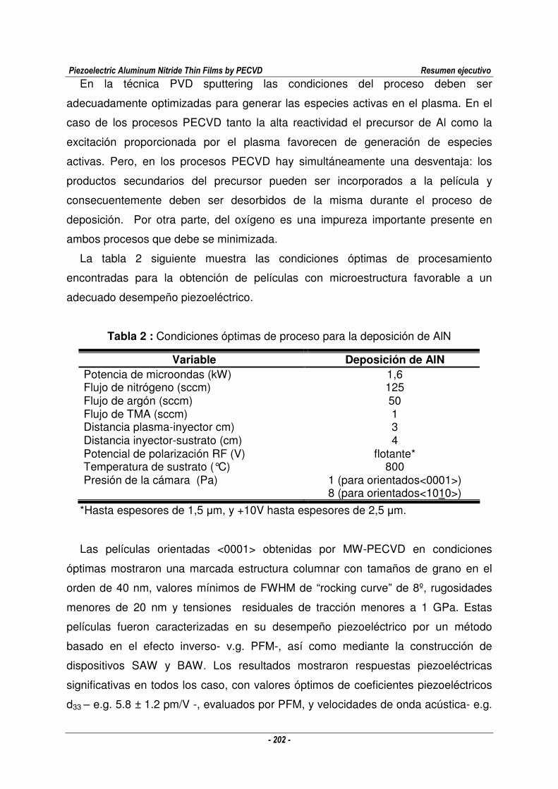
Piezoelectric Aluminum Nitride Thin Films by PECVD Resumen ejecutivo
- 202 -
En la técnica PVD sputtering las condiciones del proceso deben ser
adecuadamente optimizadas para generar las especies activas en el plasma. En el
caso de los procesos PECVD tanto la alta reactividad el precursor de Al como la
excitación proporcionada por el plasma favorecen de generación de especies
activas. Pero, en los procesos PECVD hay simultáneamente una desventaja: los
productos secundarios del precursor pueden ser incorporados a la película y
consecuentemente deben ser desorbidos de la misma durante el proceso de
deposición. Por otra parte, del oxígeno es una impureza importante presente en
ambos procesos que debe se minimizada.
La tabla 2 siguiente muestra las condiciones óptimas de procesamiento
encontradas para la obtención de películas con microestructura favorable a un
adecuado desempeño piezoeléctrico.
Tabla 2 : Condiciones óptimas de proceso para la deposición de AlN
Variable Deposición de AlN Potencia de microondas (kW) 1,6 Flujo de nitrógeno (sccm) 125 Flujo de argón (sccm) 50 Flujo de TMA (sccm) 1 Distancia plasma-inyector cm) 3 Distancia inyector-sustrato (cm) 4 Potencial de polarización RF (V) flotante* Temperatura de sustrato (°C) 800 Presión de la cámara (Pa) 1 (para orientados<0001>)
8 (para orientados<1010>)
*Hasta espesores de 1,5 µm, y +10V hasta espesores de 2,5 µm.
Las películas orientadas <0001> obtenidas por MW-PECVD en condiciones
óptimas mostraron una marcada estructura columnar con tamaños de grano en el
orden de 40 nm, valores mínimos de FWHM de “rocking curve” de 8º, rugosidades
menores de 20 nm y tensiones residuales de tracción menores a 1 GPa. Estas
películas fueron caracterizadas en su desempeño piezoeléctrico por un método
basado en el efecto inverso- v.g. PFM-, así como mediante la construcción de
dispositivos SAW y BAW. Los resultados mostraron respuestas piezoeléctricas
significativas en todos los caso, con valores óptimos de coeficientes piezoeléctricos
d33 – e.g. 5.8 ± 1.2 pm/V -, evaluados por PFM, y velocidades de onda acústica- e.g.
Piezoelectric Aluminum Nitride Thin Films by PECVD Resumen ejecutivo
- 203 -
5.05 ± 0.01 km/s-, para ondas acústicas de superficie. Estos desempeños
observados son indicativos de la ausencia de concentraciones significativas de
dominios de inversión en la microestructura de estas películas.
La evaluación del efecto de diferente parámetros sobre el coeficiente
piezoeléctrico, como la temperatura de sustrato, el espesor de película y el potencial
de polarización del portasustrato RF permitieron confirmar la importancia del
desarrollo cristalino y el grado de orientación en el desempeño piezoeléctrico de las
películas. El efecto del espesor a la temperatura óptima de proceso fue posible de
correlacionar con el desempeño piezoeléctrico a través de la construcción de
dispositivos SAW. La minimización de las tensiones residuales compresivas con la
aplicación de bajos potenciales de polarización RF mostró la posibilidad de obtener
mayores espesores con apropiada micoestructura y coeficientes piezoeléctricos
óptimos. Las diferencias en la microestructura, grado de orientación y tenor de
impurezas de oxígeno fueron directamente relacionados con el desempeño
piezoeléctrico obtenido cuando las técnicas PECVD y PVD sputtering fueron
comparadas.
El diagnóstico de plasma de proceso por OES ha permitido identificar varias
especies presentes en el medio de reacción como as Al, Al+, N2, N2+, N
directamente relacionados con el crecimiento del film. Simultáneamente, otras
especies correspondientes a productos secundarios del precursor como CN, NH, H
fueron identificados. Estos resultados fueron consistentes con la banda de
impurezas FTIR observada en los filmes de AlN obtenidos por PECVD en el entorno
de 2150 cm-1, la cual ha sido asignada a especies CN, Al-H o Al-N2 en la
bibliografía, entre otras posibilidades. Adicionalmente, fue posible evaluar el efecto
favorable de la potencia de microondas en la generación de especies activas así
como explicar el efecto negativo de adicionar hidrógeno en ese sentido. Además,
menor temperatura electrónica y menores concentraciones de especies activas
atómicas fueron estimadas a altas presiones, lo cual podría relacionarse con el
menor desarrollo cristalino observado para los filmes orientados <1010>. Asimismo,
la reducción de la temperatura electrónica con la distancia al plasma fue confirmada.
Las películas orientadas <1010> obtenidas por MW-PECVD en condiciones
óptimas mostraron una estructura no columnar con tamaños de grano en el orden de
Piezoelectric Aluminum Nitride Thin Films by PECVD Resumen ejecutivo
- 204 -
los 20 nm, valores mínimos de FWHM de “rocking curve” de 11º y rugosidades
menores a 10 nm. Estas películas no mostraron respuesta piezoeléctrica significativa
para las configuraciones ensayadas. Este era el resultado esperado para el método
PFM de acuerdo al tensor piezoeléctrico del nitruro de aluminio con estructura
cristalina tipo wurtzita. Por otra parte, la ausencia de respuesta obtenida en la
configuración SAW estándar ensayada no descarta el desempeño adecuado con
otras dimensiones del dispositivo. El campo eléctrico bajo los electrodos de las
configuraciones SAW fue modelado con el fin de mostrar que estas películas podrían
mostrar respuesta con otras geometrías más difíciles, pero posibles de construir. Si
este no fuera el caso y estas películas no tuvieran un adecuado desempeño
piezoeléctrico, la razón debería buscarse en el menor desarrollo cristalino o la
posible inversión de dominios en el plano de la superficie. Todas estas razones han
contribuido posiblemente a la ausencia de trabajos publicados donde sea evaluada
el desempeño de las películas orientadas <1010> en dispositivos SAW a pesar de
ser considerados la orientación óptima por varios autores.
Piezoelectric Aluminum Nitride Thin Films by PECVD Résumé étendu
- 205 -
Résumé étendu
COUCHES MINCES PIEZOELECTRIQUES DE
NITRURE D’ALUMINIUM PAR PECVD
Un solide est piézoélectrique quand il se polarise électriquement sous l’action d’une
force mécanique (effet direct) et est déformé mécaniquement quand un champ
électrique lui est appliqué (effet inverse).
L’origine de ce phénomène provient de la structure cristalline du solide et
particulièrement de sa symétrie. La distribution de densité électronique non uniforme
des liaisons entre les atomes produit un arrangement périodique des dipôles du
réseau cristallin. Quand une force est appliquée, la déformation générée dans le
cristal crée des changements dans les longueurs et directions des liaisons entre les
atomes du réseau. En conséquence, des changements des normes et des directions
des dipôles individuels sont induits. Ce phénomène peut conduire à une polarisation
nette du réseau cristallin, et donner lieu à l’effet piézoélectrique. Cet effet est présent
dans 20 des 21 structures cristallines non–centrosymétriques. Vu que la
piézoélectricité implique un couplage linéaire entre les systèmes mécanique et
électrique, les équations d’état qui décrivent le phénomène peuvent s’écrire comme
suit :
ii
EEdTsS .. αβαβα += (1)
j
T
ijii ETdD .. εαα += (2)
avec i, j = 1, 2, 3 et α, β = 1, 2, …6, S : déformation (m/m), D : déplacement
électrique (C/m2), T : contrainte (N/m2), E : champ électrique (V/m), sE : constante
élastique (m2/N), єT : constante diélectrique (F/m) et d : constante piézoélectrique
(m/V).
Piezoelectric Aluminum Nitride Thin Films by PECVD Résumé étendu
- 206 -
Etant donné l’emploi généralisé des énergies mécaniques et électriques dans la
vie quotidienne, les matériaux piézoélectriques offrent un grand potentiel pour le
développement de dispositifs dans de nombreuses applications électroniques. Les
dispositifs électroacoustiques basés sur des matériaux piézoélectriques, largement
employés comme oscillateurs, capteurs et résonateurs, sont très recherchés dans
l’industrie des télécommunications. Dans le secteur des communications sans fils, il
y a une importante utilisation de filtres, pour le contrôle des fréquences, sous forme
de composants à ondes acoustiques de surface (ou «surface acoustic wave», SAW)
et à ondes acoustique de volume (ou «bulk acoustic wave», BAW). La fréquence
caractéristique de fonctionnement de ces dispositifs (f, en s-1) est donnée par
l’expression :
d
VVf
20
==λ
(3)
où : V est la vitesse d’onde acoustique dans le matériau (m/s), λ0 la longueur d’onde
(m) et d la dimension caractéristique du dispositif.
Le développement important des systèmes de communication a rendu nécessaire
l’utilisation de fréquences de plus en plus élevées, qui se situent actuellement dans
le domaine des GHz, i.e. micro-ondes. L’augmentation de la fréquence (f) de
fonctionnement du dispositif est obtenue, pour un matériau donné, par réduction de
ses dimensions (d).
Ce but a été atteint avec des tailles raisonnables en utilisant des couches minces
piézoélectriques. L’utilisation de techniques de dépôt adéquates ouvre la possibilité
d’unifier les technologies de fabrication de circuits intégrés et de dispositifs
électroacoustiques.
Les caractéristiques recherchées dans un matériau utilisé pour la fabrication de
couches minces piézoélectriques dans ce secteur d’applications sont : un fort
couplage piézoélectrique, une vitesse d’onde acoustique élevée, une bonne stabilité
thermique et une faible rugosité de surface.
Le nitrure d’aluminium est piézoélectrique par sa structure cristalline hexagonale de
type wurtzite, et il présente une vitesse d’onde acoustique particulièrement élevée
grâce à ses excellentes caractéristiques mécaniques. En plus de posséder une
excellente stabilité thermique, il est caractérisé par une conductivité thermique
Piezoelectric Aluminum Nitride Thin Films by PECVD Résumé étendu
- 207 -
élevée et une énergie de bande interdite de 6,2 eV. C’est un excellent isolant
électrique quand il est pur et de composition stœchiométrique.
La performance des couches minces de nitrure d’aluminium pour des applications
piézoélectriques est directement liée à leur microstructure et leur composition.
Bien que, dans le cas idéal, il serait souhaitable d’employer des couches
monocristallines, pour les applications visées, les couches polycristallines avec une
orientation préférentielle par rapport au plan du substrat présentent d’excellentes
performances pour une production beaucoup plus simple et économique.
Les dispositifs BAW sont basés sur la génération d’ondes acoustiques
longitudinales perpendiculaires au film. Par conséquent, des couches minces
orientées selon la direction <0001>, avec l’axe c perpendiculaire à la surface du
substrat sont préférées pour optimiser le couplage piézoélectrique. Pour les
dispositifs SAW basés sur la génération d’ondes acoustiques de surface, la même
orientation est employée, bien qu’il ait été suggéré la possibilité d’utiliser l’orientation
<1010> avec l’axe c parallèle à la surface du substrat.
La qualité d’orientation des couches minces polycristallines d’AlN constitue un
paramètre important de la microstructure puisqu’elle est directement reliée aux
performances piézoélectriques du composant fabriqué. La configuration Bragg-
Brentano θ/2θ, traditionnellement employée pour l’analyse par diffraction des rayons
X (DRX) et dont le diagramme met en évidence les réflexions correspondant aux
plans parallèles au substrat, constitue une première indication de l’orientation
préférentielle de la couche. Une autre technique, dite méthode des « rocking-
curves » peut être employée pour obtenir une mesure plus fine de la dispersion dans
l’orientation de la couche par rapport à la direction de référence : la largeur à mi-
hauteur (FWHM) de la courbe obtenue est une mesure directe du degré de
désorientation du film étudié. Bien que, en général, ce dernier paramètre ait été mis
en rapport avec la performance piézoélectrique, des études récentes ont suggéré
que cette corrélation n’est pas valable dans tous les cas. La raison de cette absence
de corrélation est attribuée à la présence de grains d’orientations cristallographiques
opposées, appelés domaines d’inversion, indiscernables par DRX et difficiles à
identifier par d’autres méthodes.
Piezoelectric Aluminum Nitride Thin Films by PECVD Résumé étendu
- 208 -
Plusieurs techniques ont été employées pour obtenir des couches minces d’AlN
comme la MBE (Molecular Beam Epitaxy), MOCVD (Metal-Organic Chemical Vapor
Deposition), ou PVD (Physical Vapor Deposition) conduisant dans chaque cas à
différents types de microstructures (monocristallines, polycristallines et même
amorphes). L’obtention de couches monocristallines implique des températures
élevées ou des temps de dépôt incompatibles avec les objectifs économiques
imposés par la fabrication en masse de dispositifs.
Parmi les techniques disponibles pour l’obtention de films polycristallins, celles qui
emploient un plasma, i.e. les procédés « assistés par plasma », sont particulièrement
importants puisqu’elles permettent de réduire la température de traitement. En tenant
compte qu’un plasma est un gaz quasi-neutre composé d’électrons libres, d’ions et
d’espèces neutres, caractérisé par un comportement collectif des espèces chargées,
les plasmas de faible densité possèdent la propriété particulière d’être hors équilibre
thermodynamique, c’est-à-dire que les électrons et les espèces lourdes ont des
températures associées très différentes. Cette classe de plasma fournit l’énergie
d’activation nécessaire aux réactions chimiques grâce aux collisions inélastiques
entre les électrons libres d’énergie élevée et les molécules gazeuses, permettant
simultanément d’éviter un échauffement important du substrat. Par ailleurs, la
microstructure des couches peut être modifiée en modulant le bombardement par les
ions positifs de la couche en croissance.
Parmi les techniques assistées par plasma, on trouve les procédés PVD (Physical
Vapor Deposition) qui utilisent un transfert de matière à partir d’un matériau solide
par évaporation ou pulvérisation (« sputtering ») et les procédés CVD (Chemical
Vapor Deposition) qui consistent en l’introduction de précurseurs volatiles dans
l’enceinte de dépôt et qui, par réaction chimique, vont conduire à la formation d’un
film. Les techniques PECVD (Plasma Enhanced Chemical Vapor Deposition), et en
particulier celles qui emploient une excitation par micro-onde pour générer le plasma
offrent plusieurs avantages : a) possibilité d’ajuster plusieurs paramètres de façon à
atteindre l’optimisation des films b) possibilité de minimisation des effets de
contamination du fait de l’absence d’électrodes dans la chambre de dépôt, c)
possibilité de déposer sur substrats de géométries plus complexes, par comparaison
avec des procédés de dépôt plus directionnels comme les procédés PVD de type
pulvérisation cathodique.
Piezoelectric Aluminum Nitride Thin Films by PECVD Résumé étendu
- 209 -
Malgré les avantages énumérés, la technique PECVD avec excitation micro-ondes
n’a pas été très employée pour l’élaboration de films piézoélectriques d’AlN, et, en
aucun cas, la possibilité de contrôler l’orientation de la couche, comme <0001> ou
<1010> n’a été rapportée. Par conséquent, l’objectif du présent travail est la
détermination de l’effet des différentes variables du procédé dans le but d’obtenir des
couches minces de nitrure d’aluminium piézoélectriques orientées selon les deux
orientations indiquées.
Démarche expérimentale
Des substrats de silicium de dimensions de 30 mm x 10 mm et d’épaisseur 525 µm
ont été utilisés pour le dépôt des couches minces. Ces substrats ont été nettoyés
avec de l’éthanol et de l’acétone avant introduction dans le réacteur. Le plasma est
entretenu par une excitation micro-onde, le porte-substrat est polarisable en
radiofréquences et peut être chauffé jusqu’à 800°C. La surface des substrats a été
nettoyée in situ par un plasma d’Ar avant la phase de dépôt. Les couches d‘AlN ont
été déposées à partir d’un plasma d’azote, dans lequel a été injecté du TMA
(triméthylaluminium) acheminé jusqu’au réacteur par un gaz porteur qui était l’Ar. Les
conditions expérimentales sont reportées dans le Tableau 1.
Tableau 1: Conditions expérimentales pour l’obtention d’AlN
Variable Pré-traitement Dépôt d’AlN
Puissance micro-onde (kW) 1,0 1,6 Débit d’argon (sccm(#)) 100 50 Débit d’azote (sccm) 0 125 Tension de polarisation RF (V) - 100 -200V - flottant Pression (Pa) 0,8 0,5 – 8 Temps de process (min) 15 2 – 45 Débit de TMA (sccm) 1 Distance plasma-injecteur (mm) 30 - 110 Température de substrat (°C) 400 – 800 Distance injecteur-substrat (mm) 40 - 100 Substrat Si(100), Si(111),
Pt(111)/Si(100)
(#) Standard cubic centimeters per minute
Piezoelectric Aluminum Nitride Thin Films by PECVD Résumé étendu
- 210 -
Le travail effectué peut être divisé en trois étapes principales :
a) Croissance de couches minces d’AlN polycristallines orientées
L’influence de sept variables a été initialement étudiée pour optimiser les propriétés
des couches : la tension de polarisation RF, la distance plasma-injecteur, la
température du substrat, la pression totale, la distance injecteur-substrat, le temps de
dépôt et la nature du substrat. Comme un plan d’expériences complet aurait été trop
lourd pour vérifier l’effet de toutes les variables et leurs interactions, un travail
préliminaire a été réalisé pour connaître l’influence de la distance plasma-injecteur et
de la tension de polarisation RF appliquée au substrat. Après avoir déterminé les
valeurs adéquates de ces deux variables, les autres ont alors été étudiées en
utilisant plusieurs niveaux pour chacune.
b) Optimisation des propriétés des couches
Des expériences complémentaires ont été effectuées pour optimiser les couches en
vue d’applications électroacoustiques, en prenant les résultats de l’étude préliminaire
comme référence. Une étude paramétrique complète portant sur la température du
substrat et la pression totale a été réalisée dans le but d’optimiser le développement
de couches orientées <1010>. L’épaisseur des films et la tension de polarisation ont
été étudiées séparément en employant plusieurs niveaux pour optimiser le
développement des couches orientées <0001>. Une caractérisation plus fine de la
microstructure des couches ainsi que la mesure de leurs performances
piézoélectriques ont été réalisées à ce stade. Ceci a été complété par la
caractérisation du plasma dans différentes conditions de dépôt par spectroscopie
d’émission optique (OES).
c) Applications aux dispositifs électroacoustiques
Des dispositifs électroacoustiques de type SAW ont été préparés à partir de couches
minces d’AlN orientées <0001> et <1010> réalisées dans les conditions optimales
ainsi que des dispositifs électroacoustiques de type BAW avec des couches
orientées <0001>. Les réponses en fréquence de ces dispositifs ont été mesurées et
des modèles ont permis d’expliquer les résultats obtenus dans chaque cas.
Des diagrammes θ/2θ de diffraction de rayons X (DRX) ont été réalisés entre 15º
et 80º (2θ). La détermination de leur largeur à mi-hauteur (FWHM) des « rocking
curves » sur des couches mono-orientées a permis d’évaluer le degré d’orientation
des films.
Piezoelectric Aluminum Nitride Thin Films by PECVD Résumé étendu
- 211 -
La spectroscopie infrarouge à transformée de Fourier (IRTF) a été employée en
mode transmission entre 4000 cm-1 et 400 cm-1 et en mode réflexion.
La morphologie des couches a été analysée par microscopie à force atomique
(AFM). Le coefficient de rugosité Sa, i.e. la moyenne arithmétique de la valeur
absolue de la rugosité de surface, a été déduite de ces analyses.
L’observation des échantillons a été réalisée par microscopie électronique à
balayage (MEB), en surface et en coupe à partir de fractures. La microscopie
électronique en transmission haute résolution (HRTEM) et la diffraction électronique
(SAED) ont permis une étude fine de la microstructure du profil des couches.
La composition des couches a été analysée par la technique RBS (Rutherford
Backscattering Spectrometry) pour déterminer la teneur en aluminium, NRA (Nuclear
Reaction Analysis) pour déterminer les teneurs en carbone, azote et oxygène et la
technique XPS (X-ray photoelectron spectroscopy) pour analyser les surfaces.
La réponse piézoélectrique des couches a été évaluée par un dispositif AFM
adapté à ce type de mesures (PFM ou Piezoresponse Force Microscopy), basé sur
l’effet piézoélectrique inverse. A partir de ces mesures, le coefficient d33 du matériau
a été estimé.
Des dispositifs SAW avec une longueur d’onde acoustique de 20 µm ont été
fabriqués à partir des couches déposées en suivant un procédé de microlithographie
conventionnel. De même, des dispositifs BAW prototypes ont été fabriqués. Les
réponses en fréquences de ces dispositifs ont été déterminées en mesurant le
paramètre de transmission S21, à l’aide d’un analyseur de réseau vectoriel.
Le plasma utilisé lors de la phase de dépôt a été caractérisé par spectroscopie
d’émission optique (OES) entre 350 et 850 nm.
Résultats et discussion
Des couches minces de nitrure d’aluminium polycristallines présentant une
orientation préférentielle ont été obtenues par la technique MW-PECVD. Le choix
des paramètres de dépôt a permis la réalisation de couches orientées <0001> ou
<1010>, toutes deux intéressantes pour des applications piézoélectriques.
La réduction de la distance entre le plasma et l’injecteur de précurseur après
modification de la configuration standard du réacteur, a permis d’améliorer le
développement cristallin des films.
Piezoelectric Aluminum Nitride Thin Films by PECVD Résumé étendu
- 212 -
L’augmentation de la température de substrat a été déterminante pour améliorer la
cristallinité des couches et réduire leur teneur en impuretés.
Alors qu’il n’a pas été mis en évidence d’effets d’épitaxie en travaillant avec
différents substrats, l’analyse du profil des couches a montré une progressive
amélioration du développement cristallin avec une augmentation de l’épaisseur du
film.
La sélection de la pression de travail a permis de contrôler l’orientation
préférentielle, en obtenant des couches orientées <0001> à basse pression (1 Pa) et
des couches orientées <1010> à plus haute pression (8 Pa).
Pour de fortes valeurs de la polarisation RF, des couches amorphes présentant
des contraintes résiduelles compressives ont été obtenues. Alors que toutes les
couches obtenues au potentiel flottant présentaient des contraintes résiduelles en
tension, l’utilisation de faibles tensions de polarisation RF a permis la réduction de
cette contrainte de tension et par là même, la production de couches plus épaisses,
tout en maintenant la microstructure recherchée.
Plusieurs informations ont été obtenues sur les mécanismes généraux qui
contrôlent le développement cristallin et l’orientation préférentielle dans cette
technique de dépôt MW-PECVD.
L’accroissement des concentrations des espèces plus énergétiques et en
conséquence actives près du substrat, résultant de la réduction de la distance
plasma-injecteur, a favorisé le développement cristallin.
L’accroissement de la température du substrat pendant la phase de dépôt a
augmenté la mobilité des espèces arrivant à la surface et, en même temps, a
favorisé la désorption des impuretés associées à la décomposition du précurseur
(triméthylaluminium). En conséquence, le développement cristallin a été favorisé. En
outre, l’accroissement de la température a favorisé l’orientation <0001> des couches
réalisées à basse pression, qui correspond à l’orientation thermodynamiquement
plus favorable permettant la minimisation de l’énergie de surface.
Aucun effet d’épitaxie correspondant aux premiers instants du dépôt n’a pu être
mis en évidence. La croissance de la couche commençant de manière aléatoire,
l’orientation s’est améliorée progressivement avec l’augmentation d’épaisseur. Cette
amélioration a été fortement favorisée aux plus hautes températures.
Piezoelectric Aluminum Nitride Thin Films by PECVD Résumé étendu
- 213 -
L’augmentation de la pression a entraîné la réduction du libre parcours moyen des
espèces dans l’enceinte du réacteur et permis l’obtention de l’orientation <1010>. La
formation en phase gazeuse des dimères Al-N a été proposée comme le mécanisme
le plus adéquat pour expliquer ce phénomène, en considérant la cinétique liée au
dépôt des espèces. Bien qu’il n’ait pas été possible de détecter ces dimères avec les
techniques d’analyse disponibles, leur présence dans le mécanisme réactionnel ne
peut être écartée.
Tandis que l’orientation exclusive <0001> s’est développée à basse pression et
seulement à haute température, l’orientation exclusive <1010> s’est développée pour
les pressions élevées mais quelles que soient les températures. Il est donc possible
de conclure que des mécanismes différents contrôlent les deux phénomènes. Plus
encore, l’observation de l’orientation exclusive <1010> à toutes les températures aux
hautes pressions tend à orienter vers la théorie de formation de dimères Al-N par
rapport aux autres mécanismes qui ont été proposés pour la croissance des
couches.
Il a été montré que l’application d’une tension de polarisation RF permet le
contrôle des contraintes résiduelles en tension, mais, qu’en même temps, il existe un
autre mécanisme de contrôle de l’orientation préférentielle des films. Le
développement de contraintes résiduelles compressives élevées a favorisé le
changement d’orientation de <0001> à <1010>, associé à une relaxation des
contraintes compressives du film. Bien que ce phénomène se soit produit pour des
films de faible développement cristallin, donc non intéressants pour les applications
visées en première approximation, c’est une voie qui devrait être étudiée plus en
détails pour ces applications ou d’autres.
La comparaison de ces résultats à ceux obtenus par la technique PVD (Physical
Vapor Deposition) a conduit à la mise en évidence de similitudes concernant
l’influence des paramètres des procédés comme la pression et la tension de
polarisation du porte-substrat. Ceci montre donc qu’il devrait y avoir quelques
similitudes entre les mécanismes de croissance des deux techniques. Cependant,
quelques différences substantielles ont été démontrées en considérant les
températures de substrat nécessaires dans chacun des cas. Dans les procédés
PVD, il y a une contribution substantielle de l’énergie cinétique des espèces éjectées
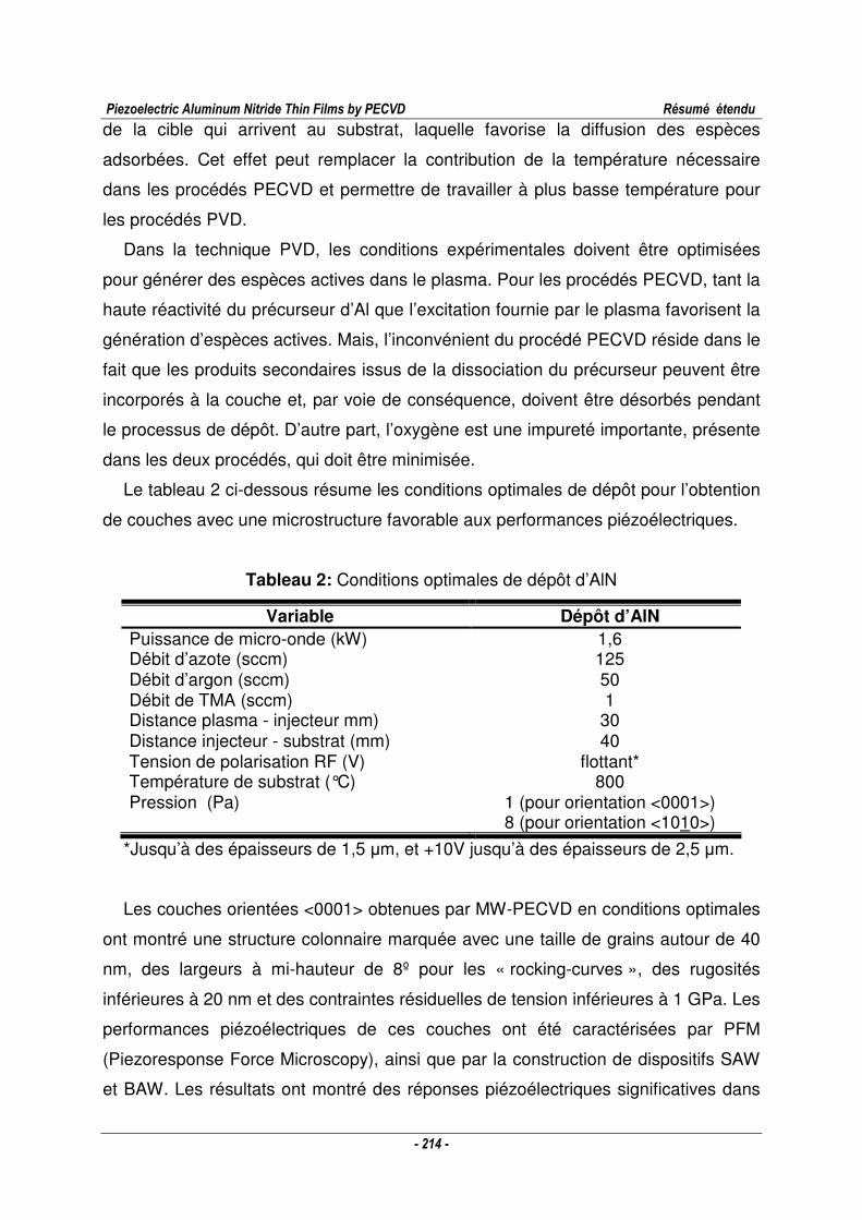
Piezoelectric Aluminum Nitride Thin Films by PECVD Résumé étendu
- 214 -
de la cible qui arrivent au substrat, laquelle favorise la diffusion des espèces
adsorbées. Cet effet peut remplacer la contribution de la température nécessaire
dans les procédés PECVD et permettre de travailler à plus basse température pour
les procédés PVD.
Dans la technique PVD, les conditions expérimentales doivent être optimisées
pour générer des espèces actives dans le plasma. Pour les procédés PECVD, tant la
haute réactivité du précurseur d’Al que l’excitation fournie par le plasma favorisent la
génération d’espèces actives. Mais, l’inconvénient du procédé PECVD réside dans le
fait que les produits secondaires issus de la dissociation du précurseur peuvent être
incorporés à la couche et, par voie de conséquence, doivent être désorbés pendant
le processus de dépôt. D’autre part, l’oxygène est une impureté importante, présente
dans les deux procédés, qui doit être minimisée.
Le tableau 2 ci-dessous résume les conditions optimales de dépôt pour l’obtention
de couches avec une microstructure favorable aux performances piézoélectriques.
Tableau 2: Conditions optimales de dépôt d’AlN
Variable Dépôt d’AlN Puissance de micro-onde (kW) 1,6 Débit d’azote (sccm) 125 Débit d’argon (sccm) 50 Débit de TMA (sccm) 1 Distance plasma - injecteur mm) 30 Distance injecteur - substrat (mm) 40 Tension de polarisation RF (V) flottant* Température de substrat (°C) 800 Pression (Pa) 1 (pour orientation <0001>)
8 (pour orientation <1010>)
*Jusqu’à des épaisseurs de 1,5 µm, et +10V jusqu’à des épaisseurs de 2,5 µm.
Les couches orientées <0001> obtenues par MW-PECVD en conditions optimales
ont montré une structure colonnaire marquée avec une taille de grains autour de 40
nm, des largeurs à mi-hauteur de 8º pour les « rocking-curves », des rugosités
inférieures à 20 nm et des contraintes résiduelles de tension inférieures à 1 GPa. Les
performances piézoélectriques de ces couches ont été caractérisées par PFM
(Piezoresponse Force Microscopy), ainsi que par la construction de dispositifs SAW
et BAW. Les résultats ont montré des réponses piézoélectriques significatives dans
Piezoelectric Aluminum Nitride Thin Films by PECVD Résumé étendu
- 215 -
tous les cas, avec des valeurs optimales de coefficients piézoélectriques d33, i.e. 5.8
± 1.2 pm/V, évaluées par PFM et de vitesses d’onde acoustique, i.e. 5.05 ± 0.01
km/s, pour des ondes acoustiques de surface. Ces valeurs prouvent l’absence de
concentrations significatives de domaines d’inversion dans la microstructure des
couches.
L’évaluation de l’effet des différents paramètres sur le coefficient piézoélectrique,
comme la température du substrat, l’épaisseur du film et la tension de polarisation
RF appliquée au porte-substrat, a permis de confirmer l’importance du
développement cristallin et du degré d’orientation sur les performances
piézoélectriques des couches. L’effet de l’épaisseur pour une température optimale
de dépôt a pu être relié aux propriétés piézoélectriques via la construction de
dispositifs SAW. La minimisation des contraintes résiduelles compressives avec
l’application de faibles tensions de polarisation RF a montré la possibilité d’obtenir de
plus grandes épaisseurs avec une microstructure appropriée et des coefficients
piézoélectriques optimaux. Les différences de microstructure, de degré d’orientation
et de teneur en oxygène ont été directement reliées aux propriétés piézoélectriques
obtenues lors de la comparaison des films réalisés respectivement par PECVD et
PVD.
Le diagnostic du plasma par la méthode OES a permis d’identifier plusieurs
espèces présentes dans le réacteur de dépôt comme Al, Al+, N2, N2+, N, à mettre
directement en rapport avec la croissance de la couche. Simultanément, d’autres
espèces à relier à des sous-produits issus de la décomposition du précurseur
comme CN, NH, H, ont été identifiées. Ces résultats sont en accord avec la bande
d’impuretés observée par FTIR autour de 2150 cm-1 dans les couches d’AlN
obtenues par PECVD, laquelle a été attribuée aux espèces CN, Al-H ou Al-N2 selon
la bibliographie. Par ailleurs, il a été possible d’évaluer l’effet favorable de la
puissance micro-onde dans la génération d’espèces actives ainsi que d’expliquer
l’effet négatif d’un ajout d’hydrogène. En outre, les plus hautes valeurs de pression
ont conduit à des températures électroniques et des concentrations d’espèces
actives atomiques plus faibles a priori, ce qui pourrait être mis en rapport avec le plus
faible développement cristallin observé pour les films orientés <1010>. De même, la
réduction de la température électronique avec la distance substrat-plasma a été
confirmée.
Piezoelectric Aluminum Nitride Thin Films by PECVD Résumé étendu
- 216 -
Les couches orientées <1010> obtenue par MW-PECVD dans les conditions
optimales ont montré une structure non colonnaire avec une taille de grains autour
de 20 nm, des valeurs de largeur à mi-hauteur des « rocking-curves » de 11º et des
rugosités inférieures à 10 nm. Ces couches n’ont pas montré de réponses
piézoélectriques significatives pour les configurations testées. Ce résultat était
attendu pour la méthode PFM, conformément au tenseur piézoélectrique du nitrure
d’aluminium pour une structure cristalline de type wurtzite. D’autre part l’absence de
réponse dans la configuration SAW standard testée n’écarte pas une possible
réponse avec d’autres dimensions du dispositif. Le champ électrique au-dessous des
électrodes des configurations SAW a été modélisé dans le but de montrer que les
couches pourraient donner une réponse pour d’autres géométries, plus complexes
mais réalisables. Si ce n’était pas le cas, la cause devrait être recherchée dans un
développement cristallin plus faible ou une possible inversion de domaines dans le
plan de la surface. Toutes ces raisons peuvent contribuer à l’absence de publications
présentant une évaluation des performances de couches orientées <1010> insérées
dans des dispositifs SAW, bien que cette orientation soit considérée comme optimale
par plusieurs auteurs.