physical modelling of advanced sige transistorselib.suub.uni-bremen.de/diss/docs/00011773.pdf ·...
TRANSCRIPT
Physical Modelling of Advanced SiGe
Transistors
Vytla Rajeev Krishna
University of Bremen 2009
Physical Modelling of Advanced SiGe
Transistors
From the Faculty of Physics/Electrical Engineering
at the University of Bremen, Germany
for the obtainment of the degree of
Doktor-Ingenieur (Dr.-Ing.)
approved thesis
by
MSc. Vytla Rajeev Krishna
from Angara, India
Supervisor: Prof. Dr. phil. nat. D. SilberCo-Supervisor: Prof. Dr. M. Schneider
Date of the oral presentation: October 13th, 2009Submitted on: September 7th, 2009

"The power of God is with you at all times; through the activities of mind,
senses, breathing, and emotions; and is constantly doing all the work using
you as a mere instrument."
— Bhagavad Gita
Acknowledgements
This dissertation would not have been completed without the help of many individuals.Firstly, I would like to thank my supervisor Prof. D. Silber at the University of Bremenfor supervising the thesis. I would like to thank Prof. M. Schneider for agreeing to be mysecond supervisor at the university. At Infineon, I would dedicate special thanks to mypresent supervisor Dr. Klaus Aufinger and Dr. Thomas Meister. This thesis would nothave been possible to complete without their support. Their influence on this work andon me as a person cannot be emphasized enough. Thanks for all the valuable commentsthey gave me, which helped me a lot in conducting my research, and thanks for all theirpatience as they reviewed and corrected my dissertation. I am forever in debt to them. Iam also grateful for all my colleagues for all their help, support, and discussions. Thankyou to all my colleagues in our group: Dzianis Lukashevich, Sabine Boguth, HerbertKnapp, Josef Böck, Herbert Schäfer, and Rudolf Lachner. Their help has solidified myresearch work. I would like to thank our team assistant Naciye Karakoc for her support.Without the support from my loving family, I would not be here today. I owe so muchto my parents, Rama Krishna and Nalini Kumari, for the support and encouragementthey gave. No words can begin to describe my deepest gratitude. I am grateful to myfriends Bhaskar, Muneet, Preethi, Ravikanth, and Naveen for their encouragement andsupport.
i
Abstract
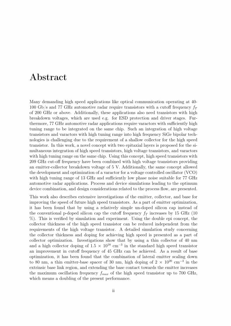
Many demanding high speed applications like optical communication operating at 40-100 Gb/s and 77 GHz automotive radar require transistors with a cutoff frequency fT
of 200 GHz or above. Additionally, these applications also need transistors with highbreakdown voltages, which are used e.g. for ESD protection and driver stages. Fur-thermore, 77 GHz automotive radar applications require varactors with sufficiently hightuning range to be integrated on the same chip. Such an integration of high voltagetransistors and varactors with high tuning range into high frequency SiGe bipolar tech-nologies is challenging due to the requirement of a shallow collector for the high speedtransistor. In this work, a novel concept with two epitaxial layers is proposed for the si-multaneous integration of high speed transistors, high voltage transistors, and varactorswith high tuning range on the same chip. Using this concept, high speed transistors with209 GHz cut-off frequency have been combined with high voltage transistors providingan emitter-collector breakdown voltage of 5 V. Additionally, the same concept allowedthe development and optimization of a varactor for a voltage controlled oscillator (VCO)with high tuning range of 13 GHz and sufficiently low phase noise suitable for 77 GHzautomotive radar applications. Process and device simulations leading to the optimumdevice combination, and design considerations related to the process flow, are presented.
This work also describes extensive investigations of the emitter, collector, and base forimproving the speed of future high speed transistors. As a part of emitter optimization,it has been found that by using a relatively simple un-doped silicon cap instead ofthe conventional p-doped silicon cap the cutoff frequency fT increases by 15 GHz (10%). This is verified by simulation and experiment. Using the double epi concept, thecollector thickness of the high speed transistor can be reduced independent from therequirements of the high voltage transistor. A detailed simulation study concerningthe collector thickness and doping for achieving high speed is presented as a part ofcollector optimization. Investigations show that by using a thin collector of 40 nmand a high collector doping of 1.5 × 1018 cm−3 in the standard high speed transistoran improvement in cutoff frequency of 45 GHz can be achieved. As a result of baseoptimization, it has been found that the combination of lateral emitter scaling downto 80 nm, a thin emitter-base spacer of 30 nm, high doping of 2 × 1020 cm−3 in theextrinsic base link region, and extending the base contact towards the emitter increasesthe maximum oscillation frequency fmax of the high speed transistor up to 700 GHz,which means a doubling of the present performance.
ii
Kurzfassung
Viele anspruchsvolle Hochfrequenzanwendungen, wie optische Nachrichtenübertragungbei 40 - 100 Gb/s und 77 GHz Abstandsradar zur Unfallverhütung im Straßenverkehrerfordern Transistoren mit Grenzfrequenzen fT von 200 GHz oder mehr. Zusätzlichbenötigen diese Anwendungen auch Transistoren mit hohen Durchbruchsspannungen,die z.B. für ESD-Schutz und Treiberschaltungen verwendet werden. Außerdem erfordern77 GHz Radaranwendungen Varaktoren mit ausreichend großem Kapazitätsverhältnis,die auf dem gleichen Chip integriert werden müssen. Solch eine Integration von Transi-storen mit hoher Durchbruchsspannung und von Varaktoren mit hohem Kapazitätsver-hältnis in Hochfrequenz-SiGe-Bipolartechnologien ist eine große Herausforderung wegender Notwendigkeit einer sehr dünnen Kollektorepitaxieschicht für den Hochgeschwindig-keitstransistor. In dieser Arbeit wird ein neues Konzept mit zwei Epitaxieschichten fürdie gleichzeitige Integration der Hochgeschwindigkeitstransistoren, der Transistoren mithoher Durchbruchsspannung und der Varaktoren mit großem Abstimmungsbereich aufdemselben Chip vorgeschlagen. Mit diesem Konzept werden Hochgeschwindigkeitstran-sistoren mit 209 GHz Grenzfrequenz mit "Hochspannungs"-Transistoren kombiniert, dieeine Emitter-Kollektor Durchbruchsspannung von 5 V aufweisen. Zusätzlich erlaubt dasgleiche Konzept die Entwicklung und Optimierung eines Varaktors mit hohem Kapaz-itätsverhältnis, der zur Herstellung eines spannungsgesteuerten Oszillators mit 13 GHzAbstimmbereich und ausreichend geringem Phasenrauschen für 77 GHz Automobil-radaranwendungen verwendet wurde. Die Prozess- und Bauelementsimulationen, diezur optimalen Bauelementkombination führten, werden dargestellt.
Diese Arbeit beschreibt weiterhin auch umfangreiche Untersuchungen aller Bauelement-bereiche (Emitter, Basis und Kollektor), um die Geschwindigkeit zukünftiger Gener-ationen von Hochgeschwindigkeitstransistoren weiter zu erhöhen. Als Teil der Opti-mierung des Emitters wurde durch Simulation gefunden, dass die Transitfrequenz fT
um 15 GHz (10%) erhöht werden kann, indem man die Schicht, in die anschließendder Arsen-Emitter diffundiert wird, zunächst undotiert abscheidet, anstatt, wie beimherkömmlichen Prozess, p-dotiert. Dieses Ergebnis wird durch das Experiment über-prüft und bestätigt. Durch Verwendung des Doppel-Epitaxie-Konzeptes kann die Dickeder Kollektorschicht des Hochgeschwindigkeitstransistors unabhängig vom Transistormit hohen Durchbruchsspannungen reduziert werden. Eine ausführliche Simulations-studie hinsichtlich der optimalen Kollektordotierung und -dicke für das Erzielen vongroßer Bauelementgeschwindigkeit wird vorgestellt. Untersuchungen zeigen, dass durch
iii
iii iv
Verwendung eines 40 nm dünnen Kollektors und einer hohen Kollektordotierung von1.5 × 1018 cm−3 eine Verbesserung der Grenzfrequenz fT um 45 GHz im Vergleich zumheutigen Transistor erzielt werden kann. Als Ergebnis der Optimierung des Basiswider-standes wurden vier Maßnahmen identifiziert, durch deren Kombination die maximaleOszillationsfrequenz fmax bis auf 700 GHz erhöht werden kann. Dies ist zunächst eineVerkleinerung der Emitterweite bis auf 80 nm und eine Reduzierung der Emitter-Basis-Spacer auf 30 nm. Ausserdem ist dazu die Bor-Dotierung im Basisanschlussgebiet auf2 × 1020 cm−3 zu erhöhen. Schließlich muss die silizierte Basisanschlusselektrode inRichtung zum Emitter hin ausgedehnt werden. Diese 700 GHz entsprechen einer Ver-dopplung des heutigen Wertes.
Contents
Acknowledgements i
Abstract ii
Kurzfassung iii
List of Figures xiv
List of Tables xix
1 Introduction 1
1.1 Motivation . . . . . . . . . . . . . . . . . . . . . . . . . . . . . . . . . . . 1
1.2 Outline . . . . . . . . . . . . . . . . . . . . . . . . . . . . . . . . . . . . . 5
2 Silicon Germanium Bipolar Technology 6
2.1 Introduction . . . . . . . . . . . . . . . . . . . . . . . . . . . . . . . . . . 6
2.2 Pseudomorphic Growth of Silicon Germanium . . . . . . . . . . . . . . . 7
2.3 Principle of SiGe HBTs . . . . . . . . . . . . . . . . . . . . . . . . . . . . 10
2.4 Figures-of-Merit . . . . . . . . . . . . . . . . . . . . . . . . . . . . . . . 13
2.4.1 Unity Current Gain Cutoff Frequency . . . . . . . . . . . . . . . . 13
2.4.2 Maximum Oscillation Frequency . . . . . . . . . . . . . . . . . . . 15
2.4.3 Breakdown Voltages . . . . . . . . . . . . . . . . . . . . . . . . . 16
2.5 Infineon’s SiGe Bipolar Technology . . . . . . . . . . . . . . . . . . . . . 17
2.5.1 Process Concept . . . . . . . . . . . . . . . . . . . . . . . . . . . 18
2.5.2 Fabrication Process . . . . . . . . . . . . . . . . . . . . . . . . . . 18
2.5.3 Electrical Characteristics . . . . . . . . . . . . . . . . . . . . . . . 24
v
CONTENTS vi
3 Device Simulation 27
3.1 Introduction . . . . . . . . . . . . . . . . . . . . . . . . . . . . . . . . . . 27
3.2 Semiconductor Equations for HBT’s . . . . . . . . . . . . . . . . . . . . . 33
3.3 Physical Model Selection . . . . . . . . . . . . . . . . . . . . . . . . . . . 36
3.3.1 Physical Models . . . . . . . . . . . . . . . . . . . . . . . . . . . . 37
3.3.2 Mobility Models . . . . . . . . . . . . . . . . . . . . . . . . . . . . 38
3.3.3 Recombination and Carrier Lifetimes . . . . . . . . . . . . . . . . 39
4 Integration of High Speed Transistors, High Voltage Transistors, and
Varactors on the Same Chip 42
4.1 Introduction of Double Epitaxy Concept . . . . . . . . . . . . . . . . . . 42
4.2 Device Structure and Fabrication Process . . . . . . . . . . . . . . . . . . 44
4.3 Device Simulation . . . . . . . . . . . . . . . . . . . . . . . . . . . . . . . 46
4.3.1 HS Transistor . . . . . . . . . . . . . . . . . . . . . . . . . . . . . 46
4.3.2 HV Transistor . . . . . . . . . . . . . . . . . . . . . . . . . . . . . 49
4.4 Electrical Transistor Results . . . . . . . . . . . . . . . . . . . . . . . . . 52
4.5 Varactor . . . . . . . . . . . . . . . . . . . . . . . . . . . . . . . . . . . . 54
4.5.1 Introduction . . . . . . . . . . . . . . . . . . . . . . . . . . . . . . 54
4.5.2 Process and Device Simulations for Varactor Optimization . . . . 56
4.5.3 Electrical Results of Varactor . . . . . . . . . . . . . . . . . . . . 65
4.6 Circuit Results for the Voltage Controlled Oscillator (VCO) . . . . . . . 68
5 Optimization of SiGe HBT for Higher Performance 70
5.1 Introduction . . . . . . . . . . . . . . . . . . . . . . . . . . . . . . . . . . 70
5.2 Emitter Optimization . . . . . . . . . . . . . . . . . . . . . . . . . . . . . 71
5.2.1 Silicon Cap Doping . . . . . . . . . . . . . . . . . . . . . . . . . . 72
5.2.2 Silicon Cap Thickness . . . . . . . . . . . . . . . . . . . . . . . . 75
5.3 Collector Thickness and Doping Optimization . . . . . . . . . . . . . . . 76
5.4 Base Optimization . . . . . . . . . . . . . . . . . . . . . . . . . . . . . . 80
5.4.1 Extrinsic Base Link Region . . . . . . . . . . . . . . . . . . . . . 81
CONTENTS vii
5.4.2 Emitter-Base Spacer . . . . . . . . . . . . . . . . . . . . . . . . . 84
5.4.3 Intrinsic Base Resistance . . . . . . . . . . . . . . . . . . . . . . . 89
5.4.4 Emitter Scaling . . . . . . . . . . . . . . . . . . . . . . . . . . . . 90
5.4.5 Extrinsic Base Contact . . . . . . . . . . . . . . . . . . . . . . . . 93
6 Summary and Outlook 102
6.1 Summary of Results and Conclusions . . . . . . . . . . . . . . . . . . . . 103
6.2 Outlook - Suggestions for Future Work . . . . . . . . . . . . . . . . . . . 105
Bibliography 106
Curriculum Vitae 112
List of Abbreviations
A Areaac Alternating currentADS Advanced Design SystemAlGaAs Aluminium Gallium ArsenideAMS Analog and Mixed SignalAs ArsenicB BoronBC Base-CollectorBJT Bipolar Junction TransistorBGN Bandgap NarrowingBiCMOS Bipolar Complementary Metal Oxide SemiconductorBL Buried LayerBV Breakdown voltageC CapacitanceCE Collector-EmitterCML Current-Mode LogicCMOS Complementary Metal Oxide SemiconductorCS Collector-SubstrateCVD Chemical Vapour DepositiondB Decibeldc Direct currentDE Double EpitaxyDPSA Double-Polysilicon Self-AlignedDOS Density of StatesDT Deep TrenchEB Emitter-BaseEHF Extremely High FrequencyESD Electro Static DischargeFLDMOB Field Dependent MobilityFOM Figure-of-MeritGe GermaniumHBT Heterojunction Bipolar TransistorHEMT High Electron Mobility Transistor
viii
HJ-AAM Heterojunction Advanced Application ModuleHS High SpeedHV High VoltageIC Integrated Circuit1-D One dimension2-D Two dimensionIFX InfineonInGaAs Indium Gallium ArsenideITRS International Technology Roadmap for SemiconductorsMOSFET Metal Oxide Semiconductor Field Effect TransistorNF Noise FigureNSEG Non Selective Epitaxial GrowthPCM Process Control MonitorPHUMOB Philips Unified Mobility ModelPSPICE Personal Computer Simulation Program with Integrated Circuit EmphasisRF Radio frequencyRTA Rapid Thermal AnnealingSEG Selective Epitaxial GrowthSi SiliconSi1−xGex, SiGe Silicon Germanium (x: Ge content)SIMS Secondary Ion Mass SpectroscopySNR Signal to Noise RatioSTI Shallow Trench IsolationSoC System on ChipSoP System-on-PackageTCAD Technology Computer Aided DesignTEM Transmission Electron MicroscopyTR Tuning Ratio
ix
List of Symbols
AE Effective emitter area
As Arsenic
Apoly Area of p+-polysilicon
Avar Active area of the varactor
BVCEO Collector-Emitter breakdown voltage
BVCBO Collector-Base breakdown voltage
β dc current gain
CBC Base-Collector capacitance
CBE Base-Emitter capacitance
Cj Junction capacitance
Cpar,ox Parasitic oxide capacitance
Dn Diffusion coefficient for electrons
Dp Diffusion coefficient for holes
Dox Oxide thickness�E Electric field
ΔEg,app Apparent bandgap narrowing
ΔEg,Ge(x = 0) Ge induced reduction in base bandgap at the EB edge of the neutralbase
ΔEg,Ge(x = wb) Ge induced reduction in base bandgap at the CB edge of the neu-tral base
�En (effective) electric field strength for electrons,�En = −∇Φ− kBT
qni∇ni
�Ep (effective) electric field strength for holes,�Ep = −∇Φ + kBT
qni∇ni
eV Electron volt
EC Conduction band edge
EV Valence band edge
x
x xi
Fn Right hand side of the electron current continuity equation
Fp Right hand side of the hole current continuity equation
fT Transit frequency, Unity current gain cutoff frequency
fmax Maximum oscillation frequency
G Net Carrier generation
Gb Base Gummel number
GII Total generation rate due to impact ionization
GIIn Total generation rate for electron impact ionization
GIIp Total generation rate for hole impact ionization
H Thermal generation
Hn Lattice heating due to electron transport
Hp Lattice heating due to hole transport
h21 Small signal current gain
JC Collector current density
Jmax Maximum current density�Jn Electron current density�Jp Hole current density
L Length of the emitter
ND Donor impurity concentration
N+D Ionized donor impurity concentration
N−
A Ionized acceptor impurity concentration
NA Acceptor impurity concentration
ni Intrinsic carrier concentration
nie Effective intrinsic carrier concentration
nib Intrinsic carrier concentration in the base
pb Majority carrier density in the base
P Phosphorus
Q Quality factor
R Net carrier recombination
Re Emitter resistance
Rb Base resistance
Rc Collector resistance
Rb,int Resistance of the active (inner) base
Rb,link Component of base resistance: Link resistance between the internaland external base including the resistance under the spacer
x xii
Rb,ext Extrinsic base resistance
Rb,tot Total base resistance
RSbi Intrinsic base sheet resistance
Rs Series resistance
Sb Antimony−→Sn Electron energy flow density−→Sp Hole energy flow density
T Lattice temperature
VA Early voltage
VBC Base-collector voltage
VBE Base-emitter voltage
VCE Collector-emitter voltage
Wmask Mask width
weff Effective emitter width
wscr Width of Space charge layer
xmj Location of metallurjical junction
xa Depletion layer edge on the anode side of the junction
xBL Location of maximum of the buried layer
xc Depletion layer edge on the cathode side of the junction
a Crystal lattice constant
c Specific heat of the material
ε Absolute permittivity
εox Permittivity of silicon oxide
ε0 Permittivity constant in vacuum ( = 8.8541878 · 10−12AsV −1m−1)
εr Relative permittivity
φn Electron quasi-Fermi potential
φp Hole quasi-Fermi potential
γ Effective density of states ratio between SiGe and Si
dox Oxide thickness
kB Boltzmann constant, kB = 1.3807 · 10−23J/K
η Minority carrier diffusion ratio between SiGe and Si
μn Electron mobility
μp Hole mobility
n Electron concentration
ni Intrinsic carrier concentration
x xiii
nie Effective intrinsic carrier concentration
p Hole concentration
q Elementary charge ( = 1.6 · 10−19 C)
ρ Mass density
ρs Surface charge density
λ Thermal conductivity of the material
sik Small signal S-parameters
τ Lifetime
τf Forward transit time
τe Emitter transit time
τb Base transit time
τc Collector transit time
τeb Emitter-base depletion layer transit time
τbc Base-collector depletion layer transit time
τn Electron lifetime in p-doped region
τp Hole lifetime in n-doped region
τwn Electron energy relaxation time
τwp Hole energy relaxation time
υsat Saturation velocity
u0 Lattice thermal energy
un Electron thermal energy
up Hole thermal energy
wB Base width
wBC Width of the base-collector space charge region
wC Collector width
wE Emitter width
yik Small signal Y-parameters
Ψ Electrostatic potential
ω Angular frequency (ω = 2πf)
χ Electron affinity
θ Band structure parameter
List of Figures
1.1 Base-collector doping profiles of a bipolar junction transistor. . . . . . . . . . 2
1.2 Excerpt from ITRS 2005, chapter on RF and AMS technologies [ITRS 06]. . . 3
1.3 ITRS fT and fmax targets for SiGe HBTs together with the region showing
best SiGe HBTs available [Schwierz 07]. . . . . . . . . . . . . . . . . . . . . 4
2.1 A comparison of strained and relaxed Si1−xGex on a silicon substrate. . . . . . 8
2.2 Bandgap as a function of germanium content for strained [King 89, Lang 85,
People 85] and unstrained [Braunstein 58] Si1−xGex. . . . . . . . . . . . . . . 9
2.3 Energy band diagram of a Si BJT and a graded-base SiGe HBT, both biased
in forward active mode at low injection [Cressler 03]. . . . . . . . . . . . . . 10
2.4 Schematic representation of bandgap reduction induced by SiGe layer with
increasing Ge content towards the collector [Cressler 03]. . . . . . . . . . . . 11
2.5 Frequency dependence of the small signal current gain |h21|2, the maximum
stable gain MSG, and the unilateral gain U [Böck 04,a]. . . . . . . . . . . . . 16
2.6 The general fT and breakdown voltage relationship for various SiGe HBTs
[Cressler 05]. . . . . . . . . . . . . . . . . . . . . . . . . . . . . . . . . . . 17
2.7 Cross section of SiGe HBT transistor with deep trench / shallow trench tran-
sistor isolation. . . . . . . . . . . . . . . . . . . . . . . . . . . . . . . . . . 19
2.8 Fabrication steps of emitter-base complex (a)-(e). . . . . . . . . . . . . . . . 21
2.9 TEM cross section of the emitter-base complex of a transistor with effective
emitter width of 0.18 μm [Böck 04,b]. . . . . . . . . . . . . . . . . . . . . . 23
2.10 SIMS doping profile of the fabricated transistors [Böck 04,b]. . . . . . . . . . 23
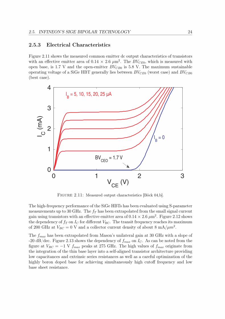
2.11 Measured output characteristics [Böck 04,b]. . . . . . . . . . . . . . . . . . . 24
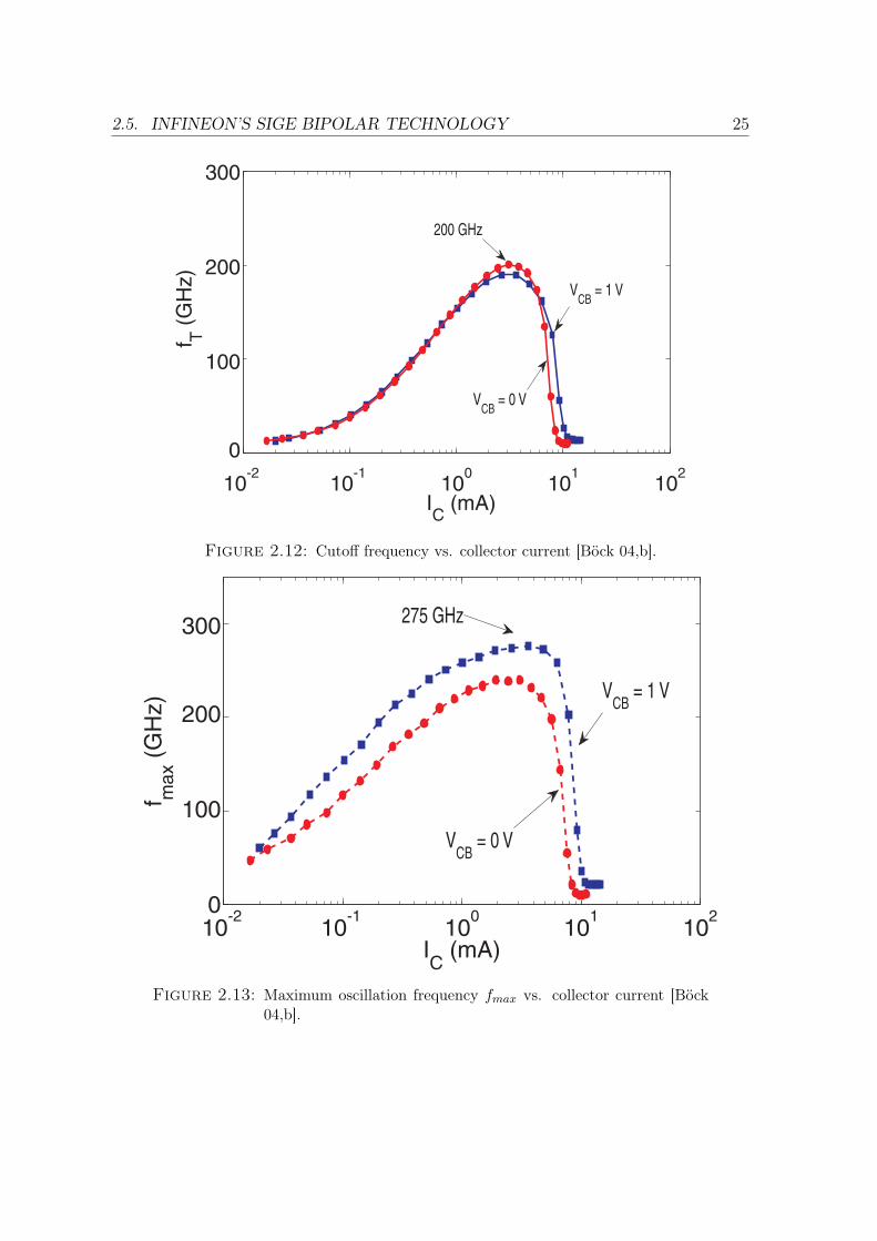
2.12 Cutoff frequency vs. collector current [Böck 04,b]. . . . . . . . . . . . . . . . 25
2.13 Maximum oscillation frequency fmax vs. collector current [Böck 04,b]. . . . . . 25
xiv
LIST OF FIGURES xv
3.1 MEDICI simulation procedure. . . . . . . . . . . . . . . . . . . . . . . . . . 28
3.2 SIMS doping profile of Infineon’s SiGe high speed transistor [Böck 04,b]. . . . 29
3.3 Typical doping profile of a SiGe HBT used for MEDICI simulations. . . . . . 30
3.4 Schematic cross section of the SiGe high speed transistor (for symmetry reasons
only half of the transistor is simulated). . . . . . . . . . . . . . . . . . . . . 30
3.5 2-D meshed SiGe HBT structure. . . . . . . . . . . . . . . . . . . . . . . . 31
3.6 Band diagram with two different materials forming a heterojunction [MEDICI
06]. . . . . . . . . . . . . . . . . . . . . . . . . . . . . . . . . . . . . . . . 35
4.1 Schematic cross section of HS transistor and HV transistor on the same substrate. 43
4.2 Fabrication of the high speed npn, high voltage npn, and varactor on the same
chip (a)-(f) [Vytla 06]. . . . . . . . . . . . . . . . . . . . . . . . . . . . . . 45
4.3 Schematic cross section of the HS transistor with an effective emitter area of
AE = 0.18 × 2.6 μm2. (For symmetry reasons, only half of the structure is
simulated.) . . . . . . . . . . . . . . . . . . . . . . . . . . . . . . . . . . . 47
4.4 Schematic cross section of the HS transistor (full structure). . . . . . . . . . . 48
4.5 Schematic representation of the vertical doping profile of the HS transistor. . 48
4.6 Comparison of experimental and simulated cutoff frequency fT vs. collector
current density JC for the HS transistor at VBC = 0 V (AE = 0.18× 2.6 μm2). 49
4.7 Schematic cross section of the simulated HV transistor (AE = 0.18× 2.6 μm2)
(For symmetry reasons, only half of the structure is simulated). . . . . . . . . 50
4.8 Schematic representation of the vertical doping profile of the HV transistor. . 50
4.9 Comparison of experimental and simulated cutoff frequency fT vs. collector
current density JC for the HV transistor at different VCB from 0 to 2 V (AE =
0.18× 2.6 μm2). . . . . . . . . . . . . . . . . . . . . . . . . . . . . . . . . 51
4.10 Measured output characteristics of high speed npn
(AE= 0.14 × 2.6 μm2). . . . . . . . . . . . . . . . . . . . . . . . . . . . . . 52
4.11 Measured output characteristics of high voltage npn
(AE= 0.14 × 2.6 μm2). . . . . . . . . . . . . . . . . . . . . . . . . . . . . . 53
4.12 Measured maximum oscillation frequency fmax vs. collector current Ic for high
voltage npn (AE= 0.14 × 2.6 μm2). . . . . . . . . . . . . . . . . . . . . . . 54
4.13 Schematic cross section of the HS transistor and varactor integrated using the
double epitaxy concept. . . . . . . . . . . . . . . . . . . . . . . . . . . . . 56
4.14 Schematic representation of a pn-junction in reverse bias. . . . . . . . . . . . 57
LIST OF FIGURES xvi
4.15 Schematic illustration of the process and device simulation for the varactor. . . 59
4.16 Flow chart describing the varactor simulation. . . . . . . . . . . . . . . . . . 60
4.17 Fabrication steps of the varactor (a)-(f). . . . . . . . . . . . . . . . . . . . . 61
4.18 Simulated 1-D vertical doping profiles of the varactor. . . . . . . . . . . . . . 62
4.19 Measured (SIMS) and fitted HV buried layer. . . . . . . . . . . . . . . . . . 63
4.20 Simulated frequency tuning characteristics of the VCO with the new varactor
with two and three implants. . . . . . . . . . . . . . . . . . . . . . . . . . . 64
4.21 Comparison of the capacitance-voltage characteristics of the measured and sim-
ulated varactor with an area of 80× 80 μm2. . . . . . . . . . . . . . . . . . . 65
4.22 Schematic cross section and layout of the varactor active area with p+- poly
overlap over oxide for estimating the oxide parasitics (figure not to scale). . . . 66
4.23 Measured capacitance-voltage characteristics of the varactor
(Avar = 5 × 1 × 10 μm2). . . . . . . . . . . . . . . . . . . . . . . . . . . . 67
4.24 Quality factor of the varactor vs. junction voltage measured at different fre-
quencies (Avar = 5 × 1 × 10 μm2). . . . . . . . . . . . . . . . . . . . . . . 68
4.25 77 GHz VCO realized using the new varactor (Chip size = 0.8 × 1.2 mm2). . . 69
4.26 Measured VCO oscillation frequency and phase noise characteristics. (Solid
line: base-collector diode of the HS transistor for frequency tuning; dashed
line: new varactor (double epitaxy concept) for frequency tuning.) . . . . . . . 69
5.1 Schematic base-emitter doping profiles of the HS transistor with p-doped, n-
doped, and un-doped silicon cap (a)-(c). . . . . . . . . . . . . . . . . . . . . 73
5.2 Simulated fT vs. IC for the HS transistor with p-doped, n-doped, and un-doped
silicon cap layers. . . . . . . . . . . . . . . . . . . . . . . . . . . . . . . . . 74
5.3 Measured fT vs. IC for the HS transistor with p-doped and un-doped silicon
cap (AE = 0.2× 2.6 μm2). . . . . . . . . . . . . . . . . . . . . . . . . . . . 74
5.4 Peak fT vs. silicon cap thickness for the HS transistor with p-doped, n-doped,
and un-doped silicon cap layers. . . . . . . . . . . . . . . . . . . . . . . . . 75
5.5 Simulated fT vs. IC for the HS transistor with an un-doped silicon cap layer
for different silicon cap thicknesses. . . . . . . . . . . . . . . . . . . . . . . . 76
5.6 Schematic base-collector doping profiles of a bipolar transistor. . . . . . . . . 77
5.7 Peak fT (a) and zero-bias base-collector capacitance CBC (b) as a function of
collector thickness and doping. . . . . . . . . . . . . . . . . . . . . . . . . . 78
5.8 PCM measurements of the HS transistor for different collector widths. . . . . 79
LIST OF FIGURES xvii
5.9 Schematic cross section of self-aligned double polysilicon bipolar transistor with
indication of parasitic base resistance contributions. . . . . . . . . . . . . . . 81
5.10 TEM (a) and schematic (b) cross section of emitter-base complex. . . . . . . . 82
5.11 Vertical doping profiles in the extrinsic base region that have been used in the
simulations. . . . . . . . . . . . . . . . . . . . . . . . . . . . . . . . . . . . 83
5.12 Top view comparison of (a) a double polysilicon transistor and (b) the test
structure. . . . . . . . . . . . . . . . . . . . . . . . . . . . . . . . . . . . . 85
5.13 Variation of the base resistance Rb,ts of the test structure with link doping. . . 86
5.14 Schematic cross section of the emitter-base portion of the HS transistor. . . . . 87
5.15 Comparison of the total base resistance Rb,tot for different link doping and
spacer thicknesses (30 nm, 50 nm, and 75 nm) for the HS transistor with a
base sheet resistance RSbi of 2.7 kΩ. . . . . . . . . . . . . . . . . . . . . . . 87
5.16 Comparison of the peak fmax at VCB = 1 V for different link doping and spacer
thicknesses (30 nm, 50 nm, and 75 nm). . . . . . . . . . . . . . . . . . . . . 88
5.17 Comparison of total base resistance Rb,tot for different link doping and spacer
thicknesses (30 nm, 50 nm, and 75 nm) for internal base sheet resistances
of 2.7 kΩ (solid) and 2.2 kΩ (dashed). The comparison is made for a device
length of 1 μm. . . . . . . . . . . . . . . . . . . . . . . . . . . . . . . . . . 89
5.18 Comparison of the peak fmax at VCB = 1 V for different link doping and spacer
thicknesses (30 nm, 50 nm, and 75 nm) for internal base sheet resistances
of 2.7 kΩ (solid) and 2.2 kΩ (dashed). . . . . . . . . . . . . . . . . . . . . . 90
5.19 Emitter-base cross section of DPSA transistor with different effective emitter
widths. . . . . . . . . . . . . . . . . . . . . . . . . . . . . . . . . . . . . . 91
5.20 High frequency performance of the HS transistor for different emitter widths. . 92
5.21 Schematic cross section of the emitter-base complex of the HS transistor (a)
without and (b) with extended base contact towards the emitter. . . . . . . . 93
5.22 Total base resistance Rb,tot vs. link doping for 30 nm spacer thickness and RSbi
of 2.2 kΩ without and with extended base contact. For comparison the case of
RSbi of 2.7 kΩ without extended base contact is also included. . . . . . . . . . 94
5.23 Peak fmax at VCB = 1 V for different link doping, 30 nm spacer thickness, and
RSbi of 2.2 kΩ without and with extended base contact (EBC). For comparison
the case of RSbi of 2.7 kΩ without extended base contact is also included. . . . 95
5.24 Enlarged schematic cross section of the emitter-base complex with base con-
tact/silicide extendeding towards the emitter. . . . . . . . . . . . . . . . . . 95
5.25 Variation of total base resistance Rb,tot and peak fmax as a function of base
contact extension towards the emitter. . . . . . . . . . . . . . . . . . . . . . 96
LIST OF FIGURES xviii
5.26 Process steps for extending the base contact of the HS transistor towards the
emitter (a)-(e). . . . . . . . . . . . . . . . . . . . . . . . . . . . . . . . . . 98
5.27 Schematic cross section of the emitter-base complex of the HS transistor with
different emitter overlaps. . . . . . . . . . . . . . . . . . . . . . . . . . . . 100
5.28 ITRS evolution for fmax and fT vs. year of production [Schwierz 07]. . . . . . 101
List of Tables
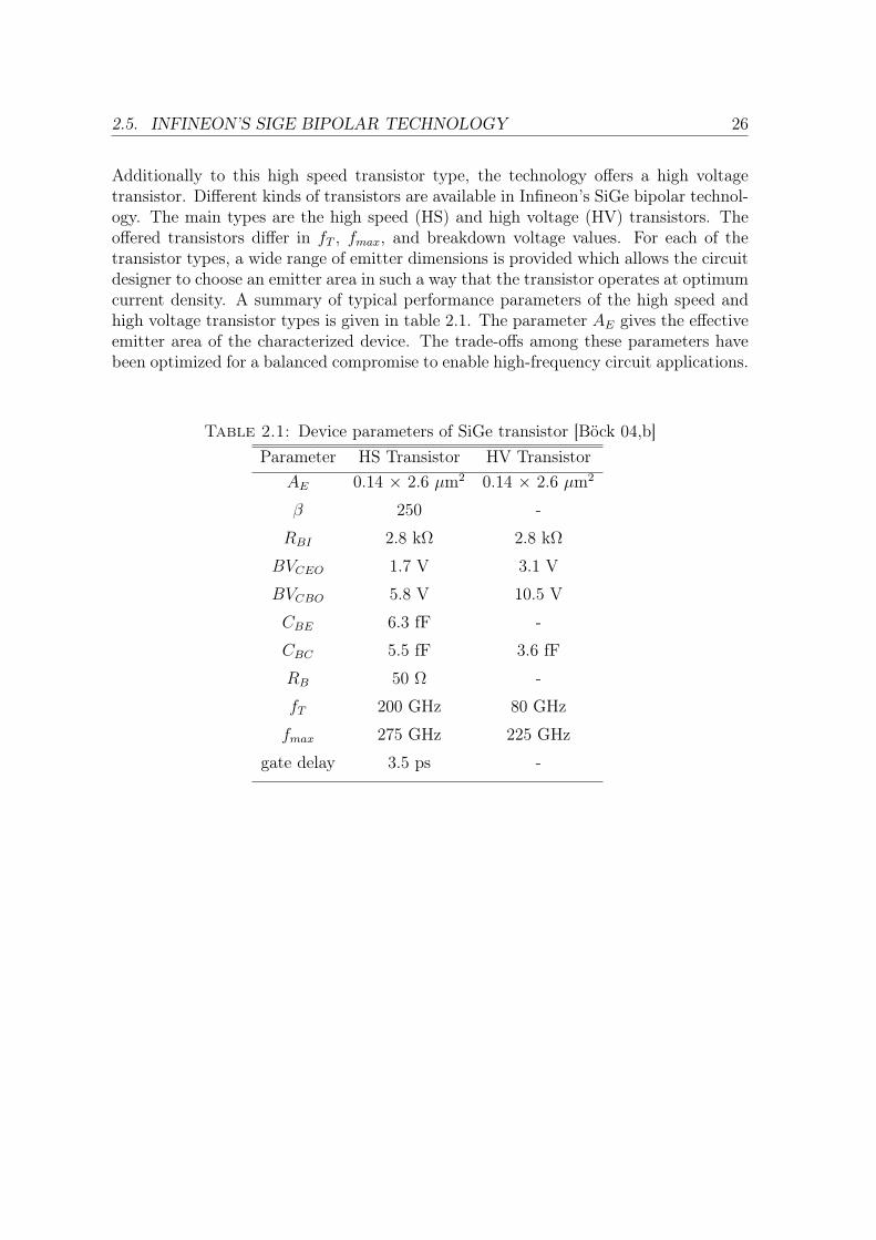
2.1 Device parameters of SiGe transistor [Böck 04,b] . . . . . . . . . . . . . . 26
3.1 MEDICI parameters . . . . . . . . . . . . . . . . . . . . . . . . . . . . . . 40
4.1 Device parameters of the HS and HV transistors [Vytla 06]. . . . . . . . . 53
4.2 Extracted varactor parameters for the varactor profile with two phosphorimplants (1 × 1013 cm−2, 80 keV / 6 × 1012 cm−2, 300 keV). . . . . . . . 63
4.3 Extracted varactor parameters for the varactor profile with three phos-phor implants (0.8 × 1013 cm−2, 80 keV / 6 × 1012 cm−2, 300 keV / 8 ×1012 cm−2, 230 keV). . . . . . . . . . . . . . . . . . . . . . . . . . . . . . 64
5.1 Comparison of zero-bias base-collector capacitance CBC and current den-sity at optimum fT for spacer thicknesses of 75, 50, and 30 nm. . . . . . 88
xix
Chapter 1
Introduction
1.1 Motivation
Future high speed applications like optical communication at 60-100 Gb/s, wirelesscommunication in the 60 GHz range, and automotive radar around 77 GHz require veryhigh speed devices. A suitable candidate for this challenging need is an ultra high speedSiGe heterojunction bipolar transistor (HBT).
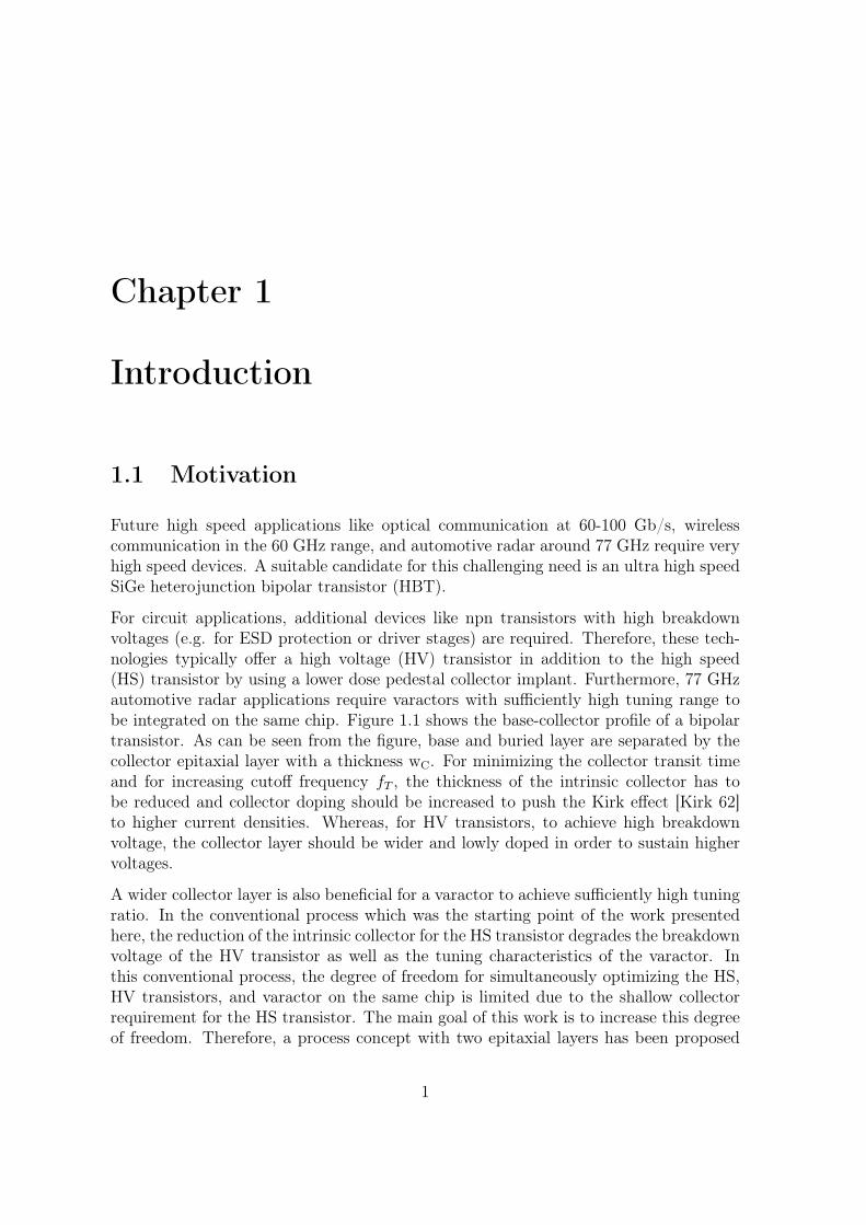
For circuit applications, additional devices like npn transistors with high breakdownvoltages (e.g. for ESD protection or driver stages) are required. Therefore, these tech-nologies typically offer a high voltage (HV) transistor in addition to the high speed(HS) transistor by using a lower dose pedestal collector implant. Furthermore, 77 GHzautomotive radar applications require varactors with sufficiently high tuning range tobe integrated on the same chip. Figure 1.1 shows the base-collector profile of a bipolartransistor. As can be seen from the figure, base and buried layer are separated by thecollector epitaxial layer with a thickness wC. For minimizing the collector transit timeand for increasing cutoff frequency fT , the thickness of the intrinsic collector has tobe reduced and collector doping should be increased to push the Kirk effect [Kirk 62]to higher current densities. Whereas, for HV transistors, to achieve high breakdownvoltage, the collector layer should be wider and lowly doped in order to sustain highervoltages.
A wider collector layer is also beneficial for a varactor to achieve sufficiently high tuningratio. In the conventional process which was the starting point of the work presentedhere, the reduction of the intrinsic collector for the HS transistor degrades the breakdownvoltage of the HV transistor as well as the tuning characteristics of the varactor. Inthis conventional process, the degree of freedom for simultaneously optimizing the HS,HV transistors, and varactor on the same chip is limited due to the shallow collectorrequirement for the HS transistor. The main goal of this work is to increase this degreeof freedom. Therefore, a process concept with two epitaxial layers has been proposed
1
1.1. MOTIVATION 2
and investigated for simultaneous optimization of HS, HV transistors, and varactor onthe same chip.
w
Figure 1.1: Base-collector doping profiles of a bipolar junction transistor.
Using this double epitaxy concept one can decouple the collector thickness of the HStransistor from that of the HV transistor and the varactor. For the HS transistor thisgives even further increased freedom for scaling the vertical collector profile for increasingthe speed performance.
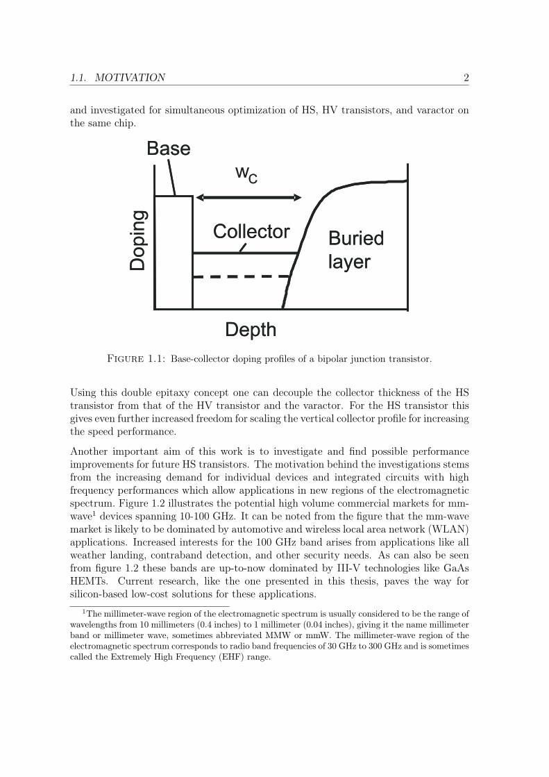
Another important aim of this work is to investigate and find possible performanceimprovements for future HS transistors. The motivation behind the investigations stemsfrom the increasing demand for individual devices and integrated circuits with highfrequency performances which allow applications in new regions of the electromagneticspectrum. Figure 1.2 illustrates the potential high volume commercial markets for mm-wave1 devices spanning 10-100 GHz. It can be noted from the figure that the mm-wavemarket is likely to be dominated by automotive and wireless local area network (WLAN)applications. Increased interests for the 100 GHz band arises from applications like allweather landing, contraband detection, and other security needs. As can also be seenfrom figure 1.2 these bands are up-to-now dominated by III-V technologies like GaAsHEMTs. Current research, like the one presented in this thesis, paves the way forsilicon-based low-cost solutions for these applications.
1The millimeter-wave region of the electromagnetic spectrum is usually considered to be the range ofwavelengths from 10 millimeters (0.4 inches) to 1 millimeter (0.04 inches), giving it the name millimeterband or millimeter wave, sometimes abbreviated MMW or mmW. The millimeter-wave region of theelectromagnetic spectrum corresponds to radio band frequencies of 30 GHz to 300 GHz and is sometimescalled the Extremely High Frequency (EHF) range.
1.1. MOTIVATION 3
Figure 1.2: Excerpt from ITRS 2005, chapter on RF and AMS technologies[ITRS 06].
Current state-of-the-art research and development for SiGe circuits is taking placeprimarily in data communication and radar systems at 24, 60, and 77 GHz [Floyd06,Katayama 07,Hajimiri 05]. For future developments, also higher frequency bands at94 and 140 GHz are of interest. Reasons for the use of higher frequency bands are thefurther miniaturization of e.g. radar systems and the better beam-forming prospectsdue to shorter wavelength.
The main drawbacks in existing designs e.g. for automotive radar, which operate typi-cally at frequencies up to a third of the cutoff frequency (fT /3), are the necessary highbias currents leading to a power dissipation of several watts per radar chip and a limitedachievable noise figure (NF) in each building block. The former disadvantage resultsin additional cooling effort, which implies costly packaging and mounting procedures.The latter directly influences the overall performance, as the total signal-to-noise ratio(SNR) in homodyne2 systems is directly limited by the NF of the (active) mixer. Toachieve low noise figure (NF) there is a need for transistors with higher fT and fmax.This can be used to optimize the future advanced system architectures. Applicationswhich do not require the higher performance of each successive transistor may insteadoperate the transistor at a lower current reducing the power dissipation. Thus, tech-nologies with higher fT can directly lead to improved automotive radar systems withhigher performance at lower power consumption, which increases road safety and lowersenergy budget. The increased HBT speed can also be utilized to improve the perfor-mance of existing applications, where SiGe HBTs are currently operated close to fT /3
2A type of receiver utilizing a local oscillator phase-locked to the incoming signal.
1.1. MOTIVATION 4
leaving only little headroom to compensate for process, voltage, and temperature vari-ations (PVT variations). With an increased fT completely new and highly integratedmicrowave sensor systems are feasible. Radar sensors at e.g. 120/140 GHz would ben-efit from reduced size structures of passives either on-chip or off-chip, especially fromminiaturized antennas.
Today’s state-of-the-art SiGe pre-production technologies have shown cutoff frequen-cies as high as fmax/fT = 350/300 GHz [Rieh 04] and 300/250 GHz [Chevalier 05].Many research and development (R&D) activities [Donkers 07, Kritivasan 06] are fo-cussed on moving SiGe HBTs into the cutoff frequency range close to 0.5 terahertz(THz) (500 GHz) enabling the future development of communication, imaging, or radarintegrated circuits (ICs) working at frequencies up to 160 GHz.
2005 2010 2015 2020100
200
300
400
500
600
700
Year
f T,f m
ax
(GH
z)
fmax
fT
fT
and fmax
of the best
SiGe HBTs (till 2007)
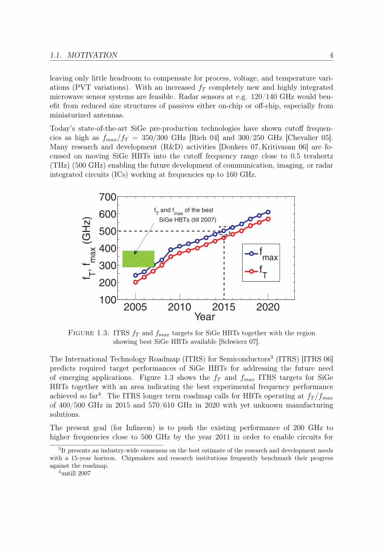
Figure 1.3: ITRS fT and fmax targets for SiGe HBTs together with the regionshowing best SiGe HBTs available [Schwierz 07].
The International Technology Roadmap (ITRS) for Semiconductors3 (ITRS) [ITRS 06]predicts required target performances of SiGe HBTs for addressing the future needof emerging applications. Figure 1.3 shows the fT and fmax ITRS targets for SiGeHBTs together with an area indicating the best experimental frequency performanceachieved so far4. The ITRS longer term roadmap calls for HBTs operating at fT /fmax
of 460/500 GHz in 2015 and 570/610 GHz in 2020 with yet unknown manufacturingsolutions.
The present goal (for Infineon) is to push the existing performance of 200 GHz tohigher frequencies close to 500 GHz by the year 2011 in order to enable circuits for
3It presents an industry-wide consensus on the best estimate of the research and development needswith a 15-year horizon. Chipmakers and research institutions frequently benchmark their progressagainst the roadmap.
4untill 2007
1.2. OUTLINE 5
target applications (e.g. 77 GHz and 140 GHz radar sensors) with much lower powerconsumption, lower noise figure, less temperature sensitivity, higher gain and yield. Thislays the foundation for the later part of this work in which various investigations areperformed for increasing the speed of future SiGe transistors.
1.2 Outline
After presenting the motivation for this thesis chapter 2 gives a short overview of the ba-sic principle of SiGe HBTs and describes Infineon’s current high frequency SiGe bipolartechnology with a cutoff frequency of 200 GHz.
Chapter 3 describes - as far as it is necessary for completely understanding the results -the device simulator (MEDICI) used for simulating the SiGe HBTs in this work. Variousphysical models and parameters for SiGe HBTs that are implemented in the simulatorare explained.
Chapter 4 presents a new process concept with two epitaxial layers (’double epi’) forintegrating high speed transistors, high voltage transistors, and varactors on the samechip. The basic concept of the "double epi" will be described. It also gives a descriptionof the fabrication process of the high speed, high voltage transistor, and varactor usingthe double epi concept. This double epi concept has been evaluated by 2-D devicesimulations and the results are discussed. The fabricated transistors are characterizedand the corresponding electrical results of the high speed and high voltage transistorsare presented. A simulation study optimizing a varactor for 77 GHz automotive radarapplications is presented. This varactor has been fabricated and the measured electricalresults are shown. The chapter concludes with the circuit results of a 77 GHz VCOwhich has been realized using the new double epi varactor.
Chapter 5 gives an overview of the investigations and device simulations performedfor increasing the speed of future high speed transistors. Key figure of merits suchas cutoff frequency and maximum oscillation frequency are discussed. As a part ofthis simulation study, different investigations of the emitter, collector, and base areperformed. In the emitter optimization, the effect of doped and un-doped silicon capregion on performance is studied by means of 1-D device simulations. As a part ofcollector investigation, variation of collector thickness and doping for improving thecutoff frequency are studied by means of 2-D device simulations. Finally, in the baseoptimization, various ways to reduce the parasitic base resistance are investigated bymeans of 2-D device simulations. These investigations include link doping variation, e-bspacer variation (lateral scaling of the spacers), intrinsic base sheet resistance reduction,lateral emitter scaling, and base contact optimizations.
Chapter 6 presents the conclusions of the present work.
Chapter 2
Silicon Germanium Bipolar Technology
This chapter reviews the electronic properties of strained SiGe and relaxed SiGe, andbriefly introduces the SiGe/Si heterostructures. Fundamental material parameters suchas the bandgap of the SiGe layers will be shown. This chapter gives the necessary insightsinto the operating behavior and properties of SiGe heterojunction and Si homojunctionbipolar technologies, both from a dc and ac perspective for an understanding of thefollowing chapters. Important figures-of-merit such as cutoff frequency fT , maximumoscillation frequency fmax, and breakdown voltages are reviewed. The process concept,the fabrication process, and the electrical results of Infineon’s actual high-frequencySiGe bipolar technology will be presented in detail.
2.1 Introduction
The basic idea of SiGe HBTs dates to the invention of BJTs in the 1950s [Shockley 51].The theoretical foundation of modern SiGe bipolar technology was developed by HerbertKrömer, who postulated that the energy bandgap of a SiGe layer could be altered withalloy grading [Krömer 57]. However, one of the most challenging tasks in the earlydevelopment of SiGe HBTs was to fabricate a very thin, high-quality SiGe base layerwhile maintaining good control over the Ge fraction, boron doping, and layer thicknessdue to the 4.1% difference between the lattice constants of Si and Ge. Thus, it has takennearly thirty years till practical techniques for the commercial production of SiGe HBTshave been developed. The first functional SiGe HBT was demonstrated in 1987 [Iyer87]. Since then, SiGe HBT technology has become widely used as a practical circuittechnology. SiGe HBTs with cutoff frequencies up to 350 GHz have been demonstrated[Rieh 02] in the past. Hence, SiGe HBT technology is challenging the superiority of III-VHBT compound semiconductor technology. The property of Si1−xGex that is of interestfor bipolar transistors is the bandgap, which is smaller than that of Si and controllableby varying the Ge content. Bandgap engineering concepts that were previously onlypossible to implement in compound semiconductor technologies, have become viable
6
2.2. PSEUDOMORPHIC GROWTH OF SILICON GERMANIUM 7
in silicon technology. These concepts have introduced a new degree of freedom in thedesign of the base, allowing the base doping to be increased and the base width to bereduced, while at the same time maintaining a reasonable value of gain. In this way,much higher values of fT and fmax have been achieved.
Due to these significant improvements in performance over Si technology and compara-tively lower manufacturing costs than III-V compound semiconductor transistors, SiGeHBTs have become a major challenger to III-V devices, which previously dominated thehigh speed and high-frequency market. Furthermore, the SiGe HBT BiCMOS technol-ogy, which integrates SiGe HBTs with best-of-breed Si CMOS, naturally offers a bettersolution in emerging System-on-Chip (SoC) and System-on-Package1 (SoP) ICs thanIII-V compound transistors.
2.2 Pseudomorphic Growth of Silicon Germanium
Silicon and germanium are completely miscible over the full range of compositions andhence can be combined to form Si1−xGex alloys with the germanium content x rangingfrom 0 to 1 (0-100%). The equilibrium lattice parameters ao for Si and Ge are 5.431and 5.646 Å, respectively [Olesinski 84]. This corresponds to a lattice mismatch to Si of
m = 100a0(Ge)− a0(Si)
a0(Si)
equal to 4.1%. When an alloy of Si and Ge is formed the equilibrium lattice parametercan roughly be linearly interpolated between Si and Ge, though there is a slight negativedeviation from Vegard’s law [Olesinski 84]. Si1−xGex has a diamond-like lattice structureand the lattice constant is given by Vegard’s rule
aSi1−xGex= aSi + x(aGe − aSi) , (2.1)
where x is the germanium fraction and a is the lattice constant. When a Si1−xGex layer isgrown on a silicon substrate, the lattice mismatch at the interface between the Si1−xGex
and the silicon has to be accommodated. This can either be done by compression of theSi1−xGex layer so that it fits to the silicon lattice or by the creation of misfit dislocationsat the interface. These two possibilities are illustrated schematically in figure 2.1. Inthe former case, the Si1−xGex layer adopts the silicon lattice spacing in the plane ofthe growth and hence the normally cubic Si1−xGex crystal is distorted (figure 2.1(b)).When Si1−xGex growth occurs in this way, the Si1−xGex layer is under compressive strainand the layer is described as pseudomorphic. In the latter case, the Si1−xGex layer is
1System-on-Package (SoP) is an emerging microelectronic technology that places an entire systemon a single chip-size package. Where "systems" used to be bulky boxes housing hundreds of compo-nents, SoP saves interconnection time and heat generation by keeping a full system with computing,communications, and consumer functions all in a single chip [Tummala 08].
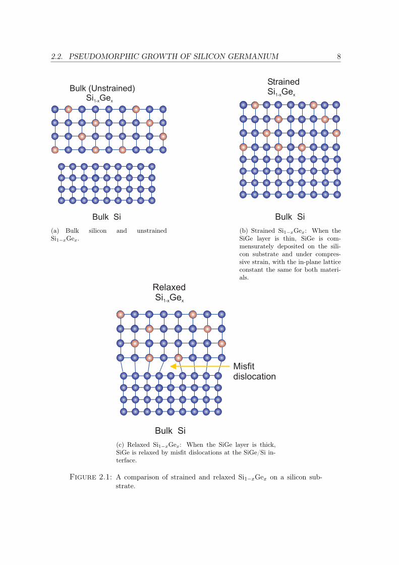
2.2. PSEUDOMORPHIC GROWTH OF SILICON GERMANIUM 8
Bulk (Unstrained)Si Ge1-x x
Bulk Si
(a) Bulk silicon and unstrainedSi1−xGex.
StrainedSi Ge1-x x
Bulk Si
(b) Strained Si1−xGex: When theSiGe layer is thin, SiGe is com-mensurately deposited on the sili-con substrate and under compres-sive strain, with the in-plane latticeconstant the same for both materi-als.
RelaxedSi Ge1-x x
Bulk Si
Misfitdislocation
(c) Relaxed Si1−xGex: When the SiGe layer is thick,SiGe is relaxed by misfit dislocations at the SiGe/Si in-terface.
Figure 2.1: A comparison of strained and relaxed Si1−xGex on a silicon sub-strate.
2.2. PSEUDOMORPHIC GROWTH OF SILICON GERMANIUM 9
unstrained, or relaxed, and the lattice mismatch at the interface is accommodated bythe formation of misfit dislocations (figure 2.1(c)).
As might be expected, there is a maximum thickness of the Si1−xGex layer that can begrown before relaxation of the strain occurs through the formation of misfit dislocations.This thickness is known as the critical thickness of the Si1−xGex layer, and dependsstrongly on the germanium content. The original calculations of critical layer thicknesswere made by Matthews and Blakeslee [Matthews 74,Matthews 75] on the basis of themechanical equilibrium of an existing threading dislocation.
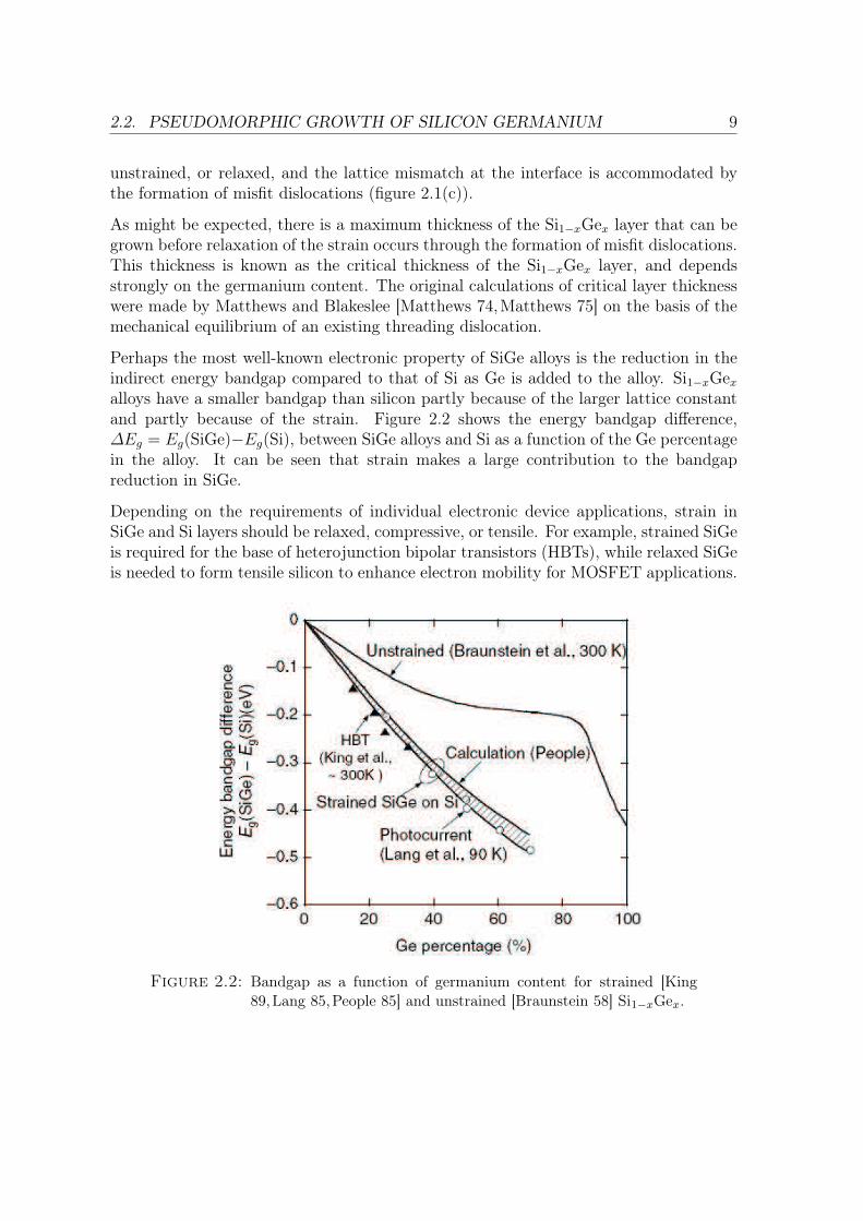
Perhaps the most well-known electronic property of SiGe alloys is the reduction in theindirect energy bandgap compared to that of Si as Ge is added to the alloy. Si1−xGex
alloys have a smaller bandgap than silicon partly because of the larger lattice constantand partly because of the strain. Figure 2.2 shows the energy bandgap difference,ΔEg = Eg(SiGe)−Eg(Si), between SiGe alloys and Si as a function of the Ge percentagein the alloy. It can be seen that strain makes a large contribution to the bandgapreduction in SiGe.
Depending on the requirements of individual electronic device applications, strain inSiGe and Si layers should be relaxed, compressive, or tensile. For example, strained SiGeis required for the base of heterojunction bipolar transistors (HBTs), while relaxed SiGeis needed to form tensile silicon to enhance electron mobility for MOSFET applications.
Figure 2.2: Bandgap as a function of germanium content for strained [King89,Lang 85,People 85] and unstrained [Braunstein 58] Si1−xGex.
2.3. PRINCIPLE OF SIGE HBTS 10
2.3 Principle of SiGe HBTs
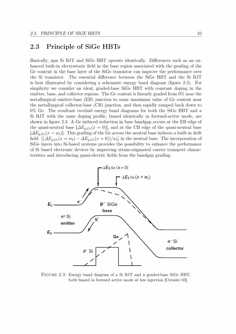
Basically, npn Si BJT and SiGe HBT operate identically. Differences such as an en-hanced built-in electrostatic field in the base region associated with the grading of theGe content in the base layer of the SiGe transistor can improve the performance overthe Si transistor. The essential difference between the SiGe HBT and the Si BJTis best illustrated by considering a schematic energy band diagram (figure 2.3). Forsimplicity we consider an ideal, graded-base SiGe HBT with constant doping in theemitter, base, and collector regions. The Ge content is linearly graded from 0% near themetallurgical emitter-base (EB) junction to some maximum value of Ge content nearthe metallurgical collector-base (CB) junction, and then rapidly ramped back down to0% Ge. The resultant overlaid energy band diagrams for both the SiGe HBT and aSi BJT with the same doping profile, biased identically in forward-active mode, areshown in figure 2.3. A Ge induced reduction in base bandgap occurs at the EB edge ofthe quasi-neutral base [ΔEg,Ge(x = 0)], and at the CB edge of the quasi-neutral base[ΔEg,Ge(x = wb)]. This grading of the Ge across the neutral base induces a built-in driftfield [(ΔEg,Ge(x = wb)−ΔEg,Ge(x = 0))/wb] in the neutral base. The incorporation ofSiGe layers into Si-based systems provides the possibility to enhance the performanceof Si based electronic devices by improving strain-originated carrier transport charac-teristics and introducing quasi-electric fields from the bandgap grading.
( )x = wb
+
-
SiGe
Si
Si
Si
Figure 2.3: Energy band diagram of a Si BJT and a graded-base SiGe HBT,both biased in forward active mode at low injection [Cressler 03].
2.3. PRINCIPLE OF SIGE HBTS 11
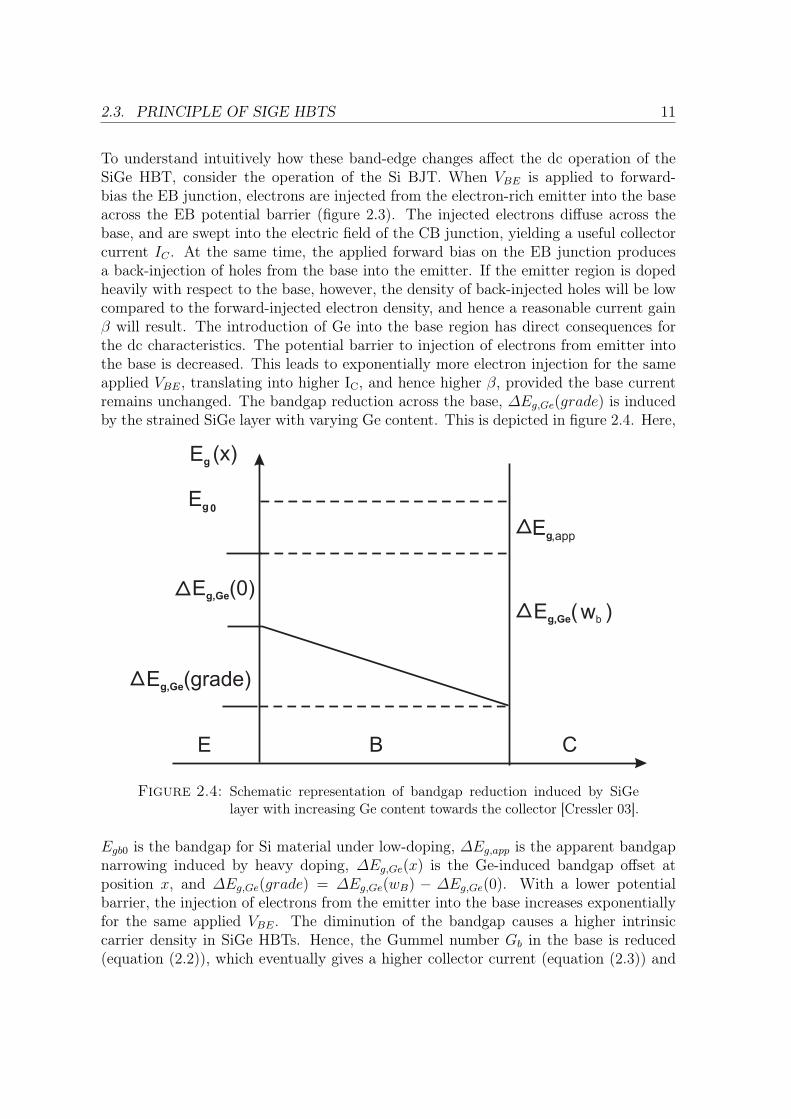
To understand intuitively how these band-edge changes affect the dc operation of theSiGe HBT, consider the operation of the Si BJT. When VBE is applied to forward-bias the EB junction, electrons are injected from the electron-rich emitter into the baseacross the EB potential barrier (figure 2.3). The injected electrons diffuse across thebase, and are swept into the electric field of the CB junction, yielding a useful collectorcurrent IC . At the same time, the applied forward bias on the EB junction producesa back-injection of holes from the base into the emitter. If the emitter region is dopedheavily with respect to the base, however, the density of back-injected holes will be lowcompared to the forward-injected electron density, and hence a reasonable current gainβ will result. The introduction of Ge into the base region has direct consequences forthe dc characteristics. The potential barrier to injection of electrons from emitter intothe base is decreased. This leads to exponentially more electron injection for the sameapplied VBE, translating into higher IC, and hence higher β, provided the base currentremains unchanged. The bandgap reduction across the base, ΔEg,Ge(grade) is inducedby the strained SiGe layer with varying Ge content. This is depicted in figure 2.4. Here,
,app
wb
Figure 2.4: Schematic representation of bandgap reduction induced by SiGelayer with increasing Ge content towards the collector [Cressler 03].
Egb0 is the bandgap for Si material under low-doping, ΔEg,app is the apparent bandgapnarrowing induced by heavy doping, ΔEg,Ge(x) is the Ge-induced bandgap offset atposition x, and ΔEg,Ge(grade) = ΔEg,Ge(wB) − ΔEg,Ge(0). With a lower potentialbarrier, the injection of electrons from the emitter into the base increases exponentiallyfor the same applied VBE. The diminution of the bandgap causes a higher intrinsiccarrier density in SiGe HBTs. Hence, the Gummel number Gb in the base is reduced(equation (2.2)), which eventually gives a higher collector current (equation (2.3)) and
2.3. PRINCIPLE OF SIGE HBTS 12
a higher β. Gb and the relation between Gb and collector current density JC is writtenas [Moll 56]
Gb =
∫ wb
0
pb(x)dx
Dn(x)n2ib(x)
, (2.2)
JC = −q(e
qVBEkT − 1)
Gb
, (2.3)
where pb is the majority carrier density in the neutral base, Dn is the minority carrierdiffusion constant in the base, nib the intrinsic carrier concentration in the base, JC isthe collector current density, and VBE is the base-emitter voltage.
Due to the difference in bandgaps of the two elements, the more Ge introduced into Si,the smaller the bandgap of the resulting alloy. The bandgap energy reduction or offsetis 75 meV per 10% mole fraction [Harame 95]. This value represents an acceptableapproximation across the practical range of 0-30% Ge content used in transistor design[Cressler 03]. The current gain ratio between SiGe HBTs and Si BJTs at a given VBE
is given by [Cressler 03]
βSiGe
βSi
|VBE≈ γηΔEg,Ge(grade) exp[ΔEg,Ge(0)/kT ]
kT{1− exp[−ΔEg,Ge(grade)/kT ]} , (2.4)
where γ is the effective density of states ratio between SiGe and Si, and η is the minoritycarrier diffusion ratio between SiGe and Si. Since this factor is dominated by the termexp[ΔEg,Ge(0)/kT ], it is clear that introducing Ge into Si strongly increases the currentgain. In addition, this current gain factor also shows that SiGe HBTs have a quasi-exponential increase of β for low temperatures.
The Early voltage VA ratio between SiGe HBT and Si BJT can be expressed as [Cressler03]
VA,SiGe
VA,Si
|VBE≈ exp[ΔEg,Ge(grade)/kT ]
{1− exp[−ΔEg,Ge(grade)/kT ]
ΔEg,Ge(grade)/kT
}, (2.5)
which gives nearly an exponential increase in VA with the Ge concentration gradientacross the base. For a typical value of ΔEg,Ge(grade) = 100 meV, the early voltage isincreased by a factor of 12. Incorporation of Ge into the intrinsic base can increase theEarly voltage by a large factor.
The graded energy bandgap also generates a quasi-electric field to enhance the transportof charged carriers in the base and induce a higher cutoff frequency fT (for a definitionof fT see next section). According to this theory, a Ge concentration gradient across thebase of an npn SiGe HBT with a lower Ge content at the emitter side generates a cor-responding quasi-electric field to aid electron transport across the base. This advantageof SiGe HBTs in high-frequency performance is represented by an enhancement in the
2.4. FIGURES-OF-MERIT 13
base and emitter transit times. The transit time ratios of τb (base transist time) and τe
(emitter transit time) are [Cressler 03]
τb,SiGe
τb,Si
≈ 2kT
ΔEg,Ge(grade)
{1− kT{1− exp[−ΔEg,Ge(grade)/kT ]}
ΔEg,Ge(grade)
}(2.6)
andτe,SiGe
τe,Si
≈ kT{1− exp[−ΔEg,Ge(grade)/kT ]}γηΔEg,Ge(grade) exp[ΔEg,Ge(0)/kT ]
, (2.7)
respectively. Both are favorably affected by either ΔEg,Ge(grade) or ΔEg,Ge(0).
From the above discussed dependencies, it is clear that the Ge can be advantageouslyused in device design. The exponential dependence of current gain β on the emitter-base boundary value of the Ge-induced band offset provides a powerful tool for tailoringβ for a specific need, and, most important, effectively makes it independent from thebase doping profile. In applications which do not require large values of β, the basecan be more heavily doped. A higher base doping is desirable for circuits because itleads to a lower intrinsic base sheet resistance. This action does not have the negativeimpact on β that would occur in the case of a BJT. If, as usual, the intrinsic base sheetresistance is a considerable fraction of the total base resistance Rb,tot (which also includescomponents due to the extrinsic region of the device, contacts, etc.), a lower intrinsicbase sheet resistance will then lead to reduced delay times in circuits and reduced noisein microwave applications.
Another benefit is an exponential enhancement in the output conductance, correspond-ing to the higher Early voltage VA. An important figure-of-merit for analog applications,such as high-speed data converters and precision current sources, is the βVA product.Since in a SiGe HBT this product depends exponentially on both the bandgap offset atthe emitter-base junction and the Ge content grading, it can thus be made very largefor applications requiring this characteristic.
2.4 Figures-of-Merit
For high-frequency ac operation, bipolar transistors are assessed with several figures-of-merit. The two most important are the unity current gain cutoff frequency fT and themaximum oscillation frequency fmax. These figures-of-merit are useful in benchmarkingtransistors and are typically given in device research publications.
2.4.1 Unity Current Gain Cutoff Frequency
fT is defined as the frequency at which common-emitter short circuit current gain isunity. It is related physically to the bipolar device as the total delay for the minority
2.4. FIGURES-OF-MERIT 14
carriers from emitter to collector, τec [Ashburn 88]. The total delay consists of the storedminority carrier recharging delay and the junction capacitance charging delay, and isrelated to fT through the following relation
fT =1
2πτec
, (2.8)
where the total transit time can be splitted into a number of various contributions ofdifferent physical origin as
τec = τe + τeb + τb + τbc + τj + CBC(Re + Rc) . (2.9)
The major components due to minority carrier stored charge are τb for the neutral baseand τbc for the base-collector space charge region. The term τe for the neutral emitterand τeb representing minority carrier transit time in the emitter-base depletion regionare often small enough to be neglected. τj is the total charging time associated with themajority carriers in the emitter-base and base-collector depletion layers. The transittime τb, the delay due to the excess minority carrier storage in the base, is generally themost significant term in equation (2.9), and the relevant expression for a SiGe HBT andthe effect of Ge grading have been given in equation (2.6).
The delay term τbc can be approximated by [Ashburn 88,Meyer 87]
τbc =wBC
2υsat
, (2.10)
where wBC is the BC depletion layer width and υsat is the carrier scattering limitedvelocity, which is approximately equal to 1× 107 cm/s at room temperature for silicon[Smith 80]. For high-speed devices, as the base width is scaled down, τb is reduced, andτe and τbc become progressively more important.
The delay term τj is given by [Sze 81]
τj =kT
qIC
(CBE + CBC) , (2.11)
where CBE and CBC are the BE and the BC depletion capacitances. As the collectorcurrent increases, it is often assumed that this transit time component becomes negligi-ble. However, for low power devices, the effect of low collector current IC on τj becomesmore significant, very clearly emphasizing the importance of minimizing the junctioncapacitances CBE and CBC .
By combining all the above equations, fT can be formulated as
1
2πfT
= τec =
⎛⎜⎜⎜⎝τe + τb + τeb +
wBC
2υsat︸ ︷︷ ︸τf
+kT
qIC
(CBE + CBC) + CBC(Re + Rc)
⎞⎟⎟⎟⎠ , (2.12)
2.4. FIGURES-OF-MERIT 15
where τf is the sum of all minority carrier contributions to τec.
We will see curves for the typical variation of fT with collector current later in this thesisseveral times (e.g. figure 2.12). From equation (2.11) it is clear that τje is dominantat low collector current, and therefore fT increases with an increase in IC . However,the influence of τje reduces as the collector current continues to increase. At peak fT ,τb, and τbc are usually the dominant terms for an optimal transistor design [Ashburn88]. Therefore, to improve the peak value of fT , all three terms need to be minimized.At high collector currents, high-injection occurs, the base transit time increases at highcollector current, causing the reduction in fT (figure 2.12).
2.4.2 Maximum Oscillation Frequency
The unity current gain cutoff frequency provides a good indication of the intrinsic delayassociated with a bipolar transistor. However, it is not a realistic indication of circuitperformance since it assumes that output is short-circuited. It also does not take intoaccount the Rb,totCBC time constant, associated with base resistance and base-collectorcapacitance. These are important parameters for determining the transient behaviorof bipolar circuits. Therefore, additionally another more practical and widely acceptedfigure-of-merit, fmax, is commonly used, which characterizes the power gain of the bipo-lar device. fmax is defined as the frequency at which the unilateral power gain becomesunity. This can be measured using s-parameter techniques, which can be easily con-verted to standard y-parameters. Unilateral gain U can be written as
U =|y12 − y21|2
4[Re(y11)Re(y22)−Re(y12)Re(y21)]. (2.13)
Using the y-parameters also various other gains such as the maximum stable gain MSGand maximum available gain MAG can be calculated as
MSG =
∣∣∣∣y21
y12
∣∣∣∣ , (2.14)
MAG =
∣∣∣∣y21
y12
∣∣∣∣ (k −
√k2 − 1
), (2.15)
where
k =2Re(y11)Re(y22)−Re(y12y21)
|y12y21| . (2.16)
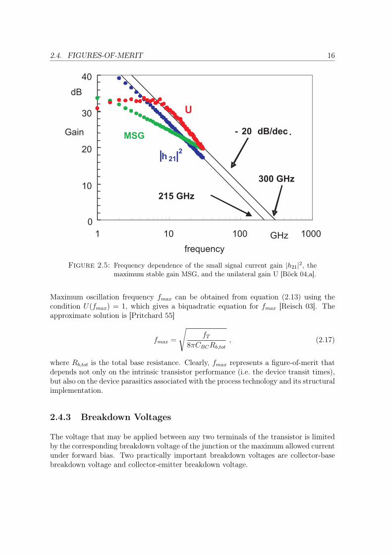
Figure 2.5 shows the frequency dependence of the small signal current gain |h21|2, theMSG, and the U of a state-of-the-art SiGe HBT [Böck 04,a] at bias conditions (VCB = 1V, IC = 3.5 mA) where fmax reaches its optimum. The maximum oscillation frequencyfmax has been extrapolated from the unilateral gain U at 25 GHz with -20dB/dec role-off.
2.4. FIGURES-OF-MERIT 16
0
10
20
30
40
1 10 100 1000
frequency
Gain
300 GHz
GHz
- 20 dB/dec .
215 GHz
U
|h 21|2
MSG
dB
Figure 2.5: Frequency dependence of the small signal current gain |h21|2, themaximum stable gain MSG, and the unilateral gain U [Böck 04,a].
Maximum oscillation frequency fmax can be obtained from equation (2.13) using thecondition U(fmax) = 1, which gives a biquadratic equation for fmax [Reisch 03]. Theapproximate solution is [Pritchard 55]
fmax =
√fT
8πCBCRb,tot
, (2.17)
where Rb,tot is the total base resistance. Clearly, fmax represents a figure-of-merit thatdepends not only on the intrinsic transistor performance (i.e. the device transit times),but also on the device parasitics associated with the process technology and its structuralimplementation.
2.4.3 Breakdown Voltages
The voltage that may be applied between any two terminals of the transistor is limitedby the corresponding breakdown voltage of the junction or the maximum allowed currentunder forward bias. Two practically important breakdown voltages are collector-basebreakdown voltage and collector-emitter breakdown voltage.
2.5. INFINEON’S SIGE BIPOLAR TECHNOLOGY 17
Collector-base breakdown Avalanche breakdown of the bc diode defines the maxi-mum reverse voltage that may be applied between collector and base with emitterleft open. The corresponding breakdown voltage, BVCBO, decreases with increas-ing values of collector doping.
Collector-emitter breakdown The open-base breakdown voltage BVCEO defines themaximum allowed voltage VCE if the base is driven with a constant current. TheBVCEO is an important design parameter, since it represents a worst-case situationfor collector-emitter breakdown.
BVCBO and BVCEO are often determined from the measured common-base and common-emitter current-voltage characteristics, respectively.
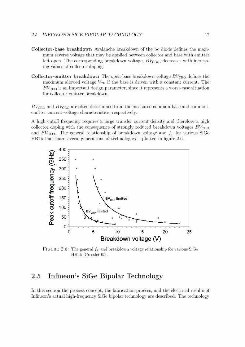
A high cutoff frequency requires a large transfer current density and therefore a highcollector doping with the consequence of strongly reduced breakdown voltages BVCBO
and BVCEO. The general relationship of breakdown voltage and fT for various SiGeHBTs that span several generations of technologies is plotted in figure 2.6.
Breakdown voltage (V)
Pea
kcu
toff
freq
ue
ncy
(GH
z)
Breakdown voltage (V)
Pea
kcu
toff
freq
ue
ncy
(GH
z)
Figure 2.6: The general fT and breakdown voltage relationship for various SiGeHBTs [Cressler 05].
2.5 Infineon’s SiGe Bipolar Technology
In this section the process concept, the fabrication process, and the electrical results ofInfineon’s actual high-frequency SiGe bipolar technology are described. The technology
2.5. INFINEON’S SIGE BIPOLAR TECHNOLOGY 18
provides a transit frequency of 200 GHz, a maximum oscillation frequency of 275 GHz,and a ring oscillator gate delay time of 3.5 ps [Böck 04,b]. Within the work of this thesisthis technology is supplemented by a new high voltage transistor and a new varactorwithout compromising the performance of the high speed npn transistor.
2.5.1 Process Concept
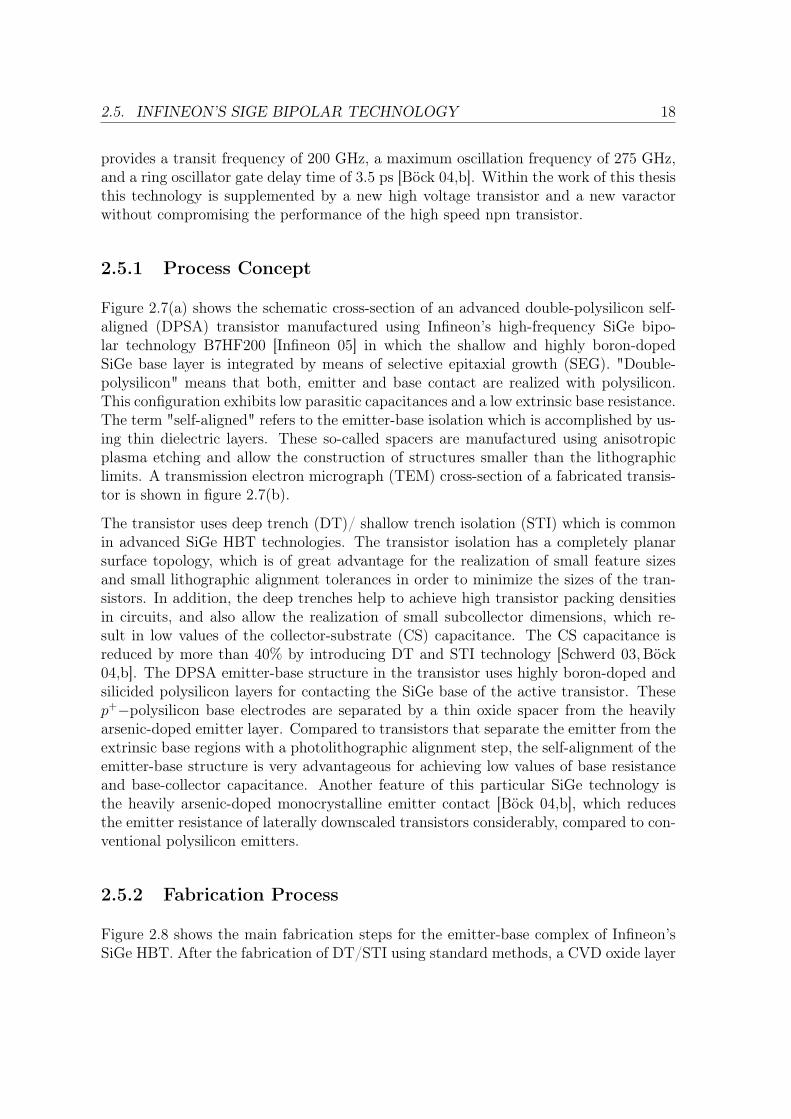
Figure 2.7(a) shows the schematic cross-section of an advanced double-polysilicon self-aligned (DPSA) transistor manufactured using Infineon’s high-frequency SiGe bipo-lar technology B7HF200 [Infineon 05] in which the shallow and highly boron-dopedSiGe base layer is integrated by means of selective epitaxial growth (SEG). "Double-polysilicon" means that both, emitter and base contact are realized with polysilicon.This configuration exhibits low parasitic capacitances and a low extrinsic base resistance.The term "self-aligned" refers to the emitter-base isolation which is accomplished by us-ing thin dielectric layers. These so-called spacers are manufactured using anisotropicplasma etching and allow the construction of structures smaller than the lithographiclimits. A transmission electron micrograph (TEM) cross-section of a fabricated transis-tor is shown in figure 2.7(b).
The transistor uses deep trench (DT)/ shallow trench isolation (STI) which is commonin advanced SiGe HBT technologies. The transistor isolation has a completely planarsurface topology, which is of great advantage for the realization of small feature sizesand small lithographic alignment tolerances in order to minimize the sizes of the tran-sistors. In addition, the deep trenches help to achieve high transistor packing densitiesin circuits, and also allow the realization of small subcollector dimensions, which re-sult in low values of the collector-substrate (CS) capacitance. The CS capacitance isreduced by more than 40% by introducing DT and STI technology [Schwerd 03,Böck04,b]. The DPSA emitter-base structure in the transistor uses highly boron-doped andsilicided polysilicon layers for contacting the SiGe base of the active transistor. Thesep+−polysilicon base electrodes are separated by a thin oxide spacer from the heavilyarsenic-doped emitter layer. Compared to transistors that separate the emitter from theextrinsic base regions with a photolithographic alignment step, the self-alignment of theemitter-base structure is very advantageous for achieving low values of base resistanceand base-collector capacitance. Another feature of this particular SiGe technology isthe heavily arsenic-doped monocrystalline emitter contact [Böck 04,b], which reducesthe emitter resistance of laterally downscaled transistors considerably, compared to con-ventional polysilicon emitters.
2.5.2 Fabrication Process
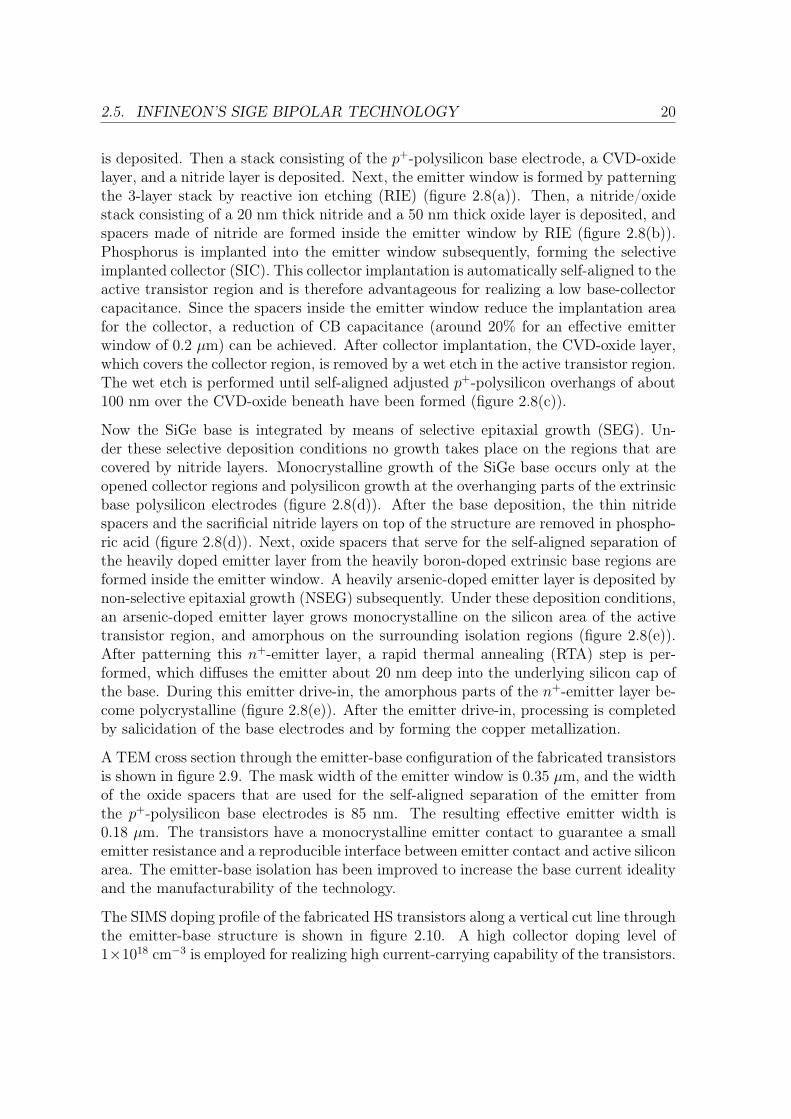
Figure 2.8 shows the main fabrication steps for the emitter-base complex of Infineon’sSiGe HBT. After the fabrication of DT/STI using standard methods, a CVD oxide layer
2.5. INFINEON’S SIGE BIPOLAR TECHNOLOGY 19
Base Emitter Collector
p--Substrate
SiC
Buried Layerp-- Isolation
STI
(Shallow Trench Iso)
n+ Poly-Si
p Mono-
SiGe:C
(Base)
p+ Poly
Silicide
DT
(Deep Trench Isolation)
Base Emitter Collector
p--Substrate
SiC
Buried Layerp-- Isolation
STI
(Shallow Trench Iso)
n Poly+
-Si
p Mono-
SiGe:C
Base
p Poly+
Silicide
DT
(Deep Trench Isolation)
(a) Schematic cross section.
SiGe base
p-poly
TEOS
500 nm
TiSi2
collector emitter base
shallow trench
deep trench
SiGe baseSiGe base
p-poly
TEOS
500 nm
TiSi2
collector emitter base
shallow trench
deep trench
SiGe base
(b) TEM cross section [Böck 04,b].
Figure 2.7: Cross section of SiGe HBT transistor with deep trench / shallowtrench transistor isolation.
2.5. INFINEON’S SIGE BIPOLAR TECHNOLOGY 20
is deposited. Then a stack consisting of the p+-polysilicon base electrode, a CVD-oxidelayer, and a nitride layer is deposited. Next, the emitter window is formed by patterningthe 3-layer stack by reactive ion etching (RIE) (figure 2.8(a)). Then, a nitride/oxidestack consisting of a 20 nm thick nitride and a 50 nm thick oxide layer is deposited, andspacers made of nitride are formed inside the emitter window by RIE (figure 2.8(b)).Phosphorus is implanted into the emitter window subsequently, forming the selectiveimplanted collector (SIC). This collector implantation is automatically self-aligned to theactive transistor region and is therefore advantageous for realizing a low base-collectorcapacitance. Since the spacers inside the emitter window reduce the implantation areafor the collector, a reduction of CB capacitance (around 20% for an effective emitterwindow of 0.2 μm) can be achieved. After collector implantation, the CVD-oxide layer,which covers the collector region, is removed by a wet etch in the active transistor region.The wet etch is performed until self-aligned adjusted p+-polysilicon overhangs of about100 nm over the CVD-oxide beneath have been formed (figure 2.8(c)).
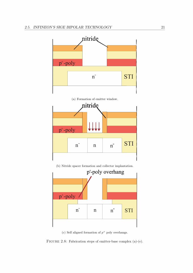
Now the SiGe base is integrated by means of selective epitaxial growth (SEG). Un-der these selective deposition conditions no growth takes place on the regions that arecovered by nitride layers. Monocrystalline growth of the SiGe base occurs only at theopened collector regions and polysilicon growth at the overhanging parts of the extrinsicbase polysilicon electrodes (figure 2.8(d)). After the base deposition, the thin nitridespacers and the sacrificial nitride layers on top of the structure are removed in phospho-ric acid (figure 2.8(d)). Next, oxide spacers that serve for the self-aligned separation ofthe heavily doped emitter layer from the heavily boron-doped extrinsic base regions areformed inside the emitter window. A heavily arsenic-doped emitter layer is deposited bynon-selective epitaxial growth (NSEG) subsequently. Under these deposition conditions,an arsenic-doped emitter layer grows monocrystalline on the silicon area of the activetransistor region, and amorphous on the surrounding isolation regions (figure 2.8(e)).After patterning this n+-emitter layer, a rapid thermal annealing (RTA) step is per-formed, which diffuses the emitter about 20 nm deep into the underlying silicon cap ofthe base. During this emitter drive-in, the amorphous parts of the n+-emitter layer be-come polycrystalline (figure 2.8(e)). After the emitter drive-in, processing is completedby salicidation of the base electrodes and by forming the copper metallization.
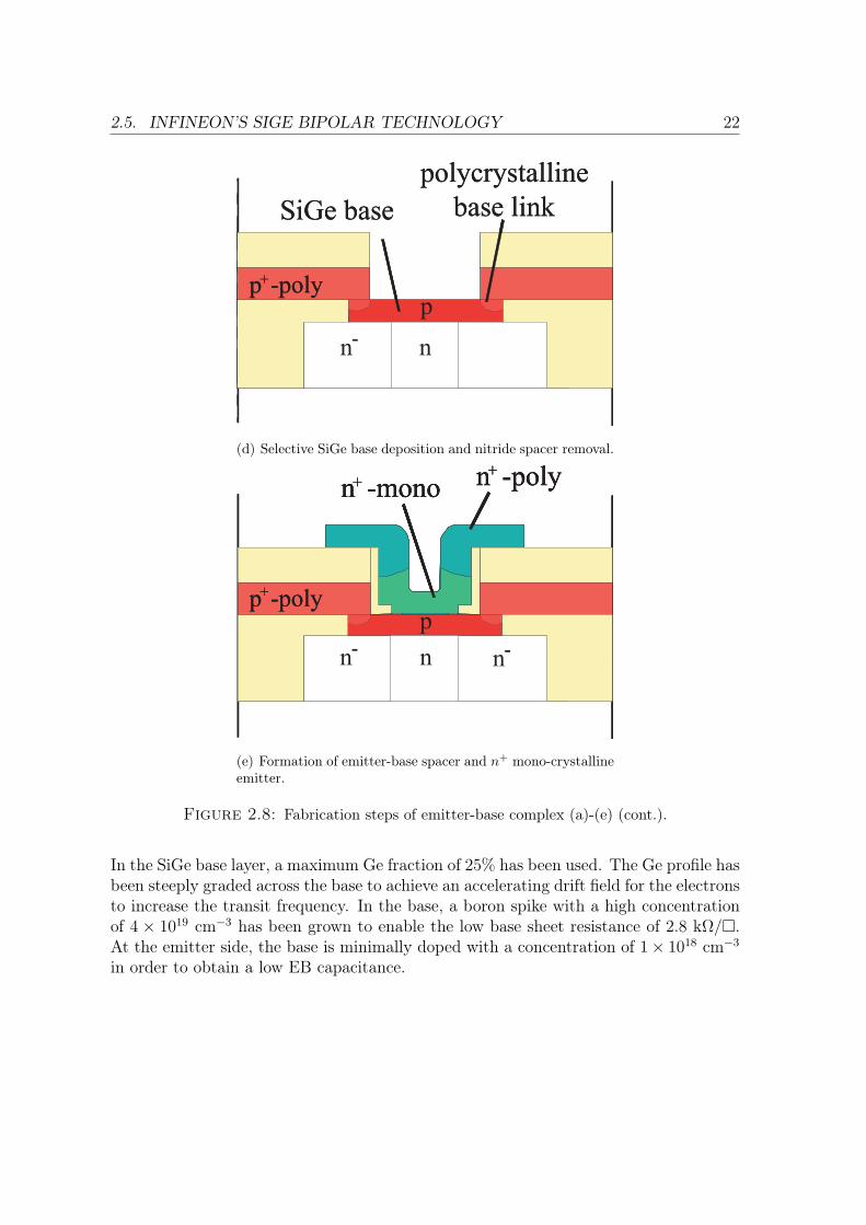
A TEM cross section through the emitter-base configuration of the fabricated transistorsis shown in figure 2.9. The mask width of the emitter window is 0.35 μm, and the widthof the oxide spacers that are used for the self-aligned separation of the emitter fromthe p+-polysilicon base electrodes is 85 nm. The resulting effective emitter width is0.18 μm. The transistors have a monocrystalline emitter contact to guarantee a smallemitter resistance and a reproducible interface between emitter contact and active siliconarea. The emitter-base isolation has been improved to increase the base current idealityand the manufacturability of the technology.
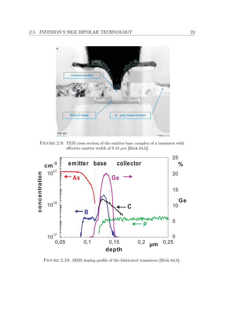
The SIMS doping profile of the fabricated HS transistors along a vertical cut line throughthe emitter-base structure is shown in figure 2.10. A high collector doping level of1×1018 cm−3 is employed for realizing high current-carrying capability of the transistors.
2.5. INFINEON’S SIGE BIPOLAR TECHNOLOGY 21
nitride
p+-poly
STIn-
nitride
p+-poly
STIn-
(a) Formation of emitter window.
nitride
p+-poly
STIn-nn-
n-
nitride
p+-poly
STIn-
nitride
p+-poly
STIn-
nitride
p+-poly
STInn-n-
(b) Nitride spacer formation and collector implantation.
p+-poly
nn-n-
p+-poly overhang
STI
p+-poly
nn-n-
p+-poly overhang
STI
(c) Self aligned formation of p+ poly overhangs.
Figure 2.8: Fabrication steps of emitter-base complex (a)-(e).
2.5. INFINEON’S SIGE BIPOLAR TECHNOLOGY 22
SiGe base
p
nn-
polycrystalline
base link
p+-poly
SiGe base
p
nn-
polycrystalline
base link
p+-polyp+-poly
(d) Selective SiGe base deposition and nitride spacer removal.
n+ -poly
pp+-poly
n+ -mono
nn-n-
p+-poly
n+ -poly
pp+-poly
n+ -mono
nn-n-
n+ -poly
pp+-poly
n+ -mono
nn-n-
p+-polyp+-poly
(e) Formation of emitter-base spacer and n+ mono-crystallineemitter.
Figure 2.8: Fabrication steps of emitter-base complex (a)-(e) (cont.).
In the SiGe base layer, a maximum Ge fraction of 25% has been used. The Ge profile hasbeen steeply graded across the base to achieve an accelerating drift field for the electronsto increase the transit frequency. In the base, a boron spike with a high concentrationof 4 × 1019 cm−3 has been grown to enable the low base sheet resistance of 2.8 kΩ/�.At the emitter side, the base is minimally doped with a concentration of 1× 1018 cm−3
in order to obtain a low EB capacitance.
2.5. INFINEON’S SIGE BIPOLAR TECHNOLOGY 23
SiGe:C base
n-mono-emitter
p+ -poly base contactSiGe:C base
n-mono-emitter
p+ -poly base contact
Figure 2.9: TEM cross section of the emitter-base complex of a transistor witheffective emitter width of 0.18 μm [Böck 04,b].
Figure 2.10: SIMS doping profile of the fabricated transistors [Böck 04,b].
2.5. INFINEON’S SIGE BIPOLAR TECHNOLOGY 24
2.5.3 Electrical Characteristics
Figure 2.11 shows the measured common emitter dc output characteristics of transistorswith an effective emitter area of 0.14 × 2.6 μm2. The BVCE0, which is measured withopen base, is 1.7 V and the open-emitter BVCB0 is 5.8 V. The maximum sustainableoperating voltage of a SiGe HBT generally lies between BVCE0 (worst case) and BVCB0
(best case).
0 1 2 30
1
2
3
4
VCE
(V)
I C(m
A)
BVCEO
= 1.7 V
IB
= 0
IB
= 5, 10, 15, 20, 25 μA
Figure 2.11: Measured output characteristics [Böck 04,b].
The high-frequency performance of the SiGe HBTs has been evaluated using S-parametermeasurements up to 30 GHz. The fT has been extrapolated from the small signal currentgain using transistors with an effective emitter area of 0.14 × 2.6 μm2. Figure 2.12 showsthe dependency of fT on IC for different VBC. The transit frequency reaches its maximumof 200 GHz at VBC = 0 V and a collector current density of about 8 mA/μm2.
The fmax has been extrapolated from Mason’s unilateral gain at 30 GHz with a slope of-20 dB/dec. Figure 2.13 shows the dependency of fmax on IC . As can be noted from thefigure at VBC = −1 V fmax peaks at 275 GHz. The high values of fmax originate fromthe integration of the thin base layer into a self-aligned transistor architecture providinglow capacitances and extrinsic series resistances as well as a careful optimization of thehighly boron doped base for achieving simultaneously high cutoff frequency and lowbase sheet resistance.
2.5. INFINEON’S SIGE BIPOLAR TECHNOLOGY 25
10-2
10-1
100
101
102
0
100
200
300
IC
(mA)
f T(G
Hz)
VCB
= 0 V
VCB
= 1 V
200 GHz
Figure 2.12: Cutoff frequency vs. collector current [Böck 04,b].
10-2
10-1
100
101
102
0
100
200
300
IC
(mA)
f max
(GH
z)
VCB
= 0 V
VCB
= 1 V
275 GHz
Figure 2.13: Maximum oscillation frequency fmax vs. collector current [Böck04,b].
2.5. INFINEON’S SIGE BIPOLAR TECHNOLOGY 26
Additionally to this high speed transistor type, the technology offers a high voltagetransistor. Different kinds of transistors are available in Infineon’s SiGe bipolar technol-ogy. The main types are the high speed (HS) and high voltage (HV) transistors. Theoffered transistors differ in fT , fmax, and breakdown voltage values. For each of thetransistor types, a wide range of emitter dimensions is provided which allows the circuitdesigner to choose an emitter area in such a way that the transistor operates at optimumcurrent density. A summary of typical performance parameters of the high speed andhigh voltage transistor types is given in table 2.1. The parameter AE gives the effectiveemitter area of the characterized device. The trade-offs among these parameters havebeen optimized for a balanced compromise to enable high-frequency circuit applications.
Table 2.1: Device parameters of SiGe transistor [Böck 04,b]
Parameter HS Transistor HV Transistor
AE 0.14 × 2.6 μm2 0.14 × 2.6 μm2
β 250 -
RBI 2.8 kΩ 2.8 kΩ
BVCEO 1.7 V 3.1 V
BVCBO 5.8 V 10.5 V
CBE 6.3 fF -
CBC 5.5 fF 3.6 fF
RB 50 Ω -
fT 200 GHz 80 GHz
fmax 275 GHz 225 GHz
gate delay 3.5 ps -
Chapter 3
Device Simulation
This chapter describes - as far as it is necessary for completely understanding the results- the device simulator MEDICI used for simulating the SiGe HBTs in this work. Variousphysical models and parameters for SiGe HBTs that are implemented in the simulatorare explained.
3.1 Introduction
Numerical simulation is a very powerful tool in the semiconductor industry especially forpredicting the main properties of novel devices without the need for fabricating them.Such simulations offer the possibility to include various materials and different physicalmodels for the various effects that need to be considered. The use of numerical simu-lation has become more important in the semiconductor industry because it is a toolthat has proven to be able to provide accurate prediction for future devices. This is im-portant for working towards the fulfillment of the international technology roadmap forsemiconductors (ITRS), which requires drastic changes in today’s available technology.Another factor that has pushed the use of numerical simulation as a major tool today isthe cost factor. Due to the drastic rise in costs for technology development, numericalsimulation is a cheap but efficient method to analyze and predict the characteristics offuture devices before fabricating the real device or even before the technology becomesavailable.
Numerical analysis based on the fundamental equations governing electronic transportin semiconductors is widely used. The powerful device simulator MEDICI [MEDICI 06]is used in this thesis for 1-D and 2-D simulations. MEDICI is an industry-standarddevice simulation tool developed by Synopsys to predict the electrical, thermal, andoptical characteristics of semiconductor devices using advanced physical models for allnecessary effects like Shockley-Read-Hall (SRH) and Auger recombination, avalanchebreakdown, and bandgap narrowing (BGN).
27
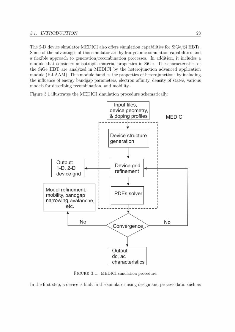
3.1. INTRODUCTION 28
The 2-D device simulator MEDICI also offers simulation capabilities for SiGe/Si HBTs.Some of the advantages of this simulator are hydrodynamic simulation capabilities anda flexible approach to generation/recombination processes. In addition, it includes amodule that considers anisotropic material properties in SiGe. The characteristics ofthe SiGe HBT are analyzed in MEDICI by the heterojunction advanced applicationmodule (HJ-AAM). This module handles the properties of heterojunctions by includingthe influence of energy bandgap parameters, electron affinity, density of states, variousmodels for describing recombination, and mobility.
Figure 3.1 illustrates the MEDICI simulation procedure schematically.
Device structuregeneration
Input files,device geometry,& doping profiles
Device gridrefinement
PDEs solver
Convergence
Output:dc, accharacteristics
NoNo
Model refinement:mobility, bandgap
avalanche,
Output:1-D, 2-Ddevice grid
MEDICI
narrowing,etc.
Figure 3.1: MEDICI simulation procedure.
In the first step, a device is built in the simulator using design and process data, such as
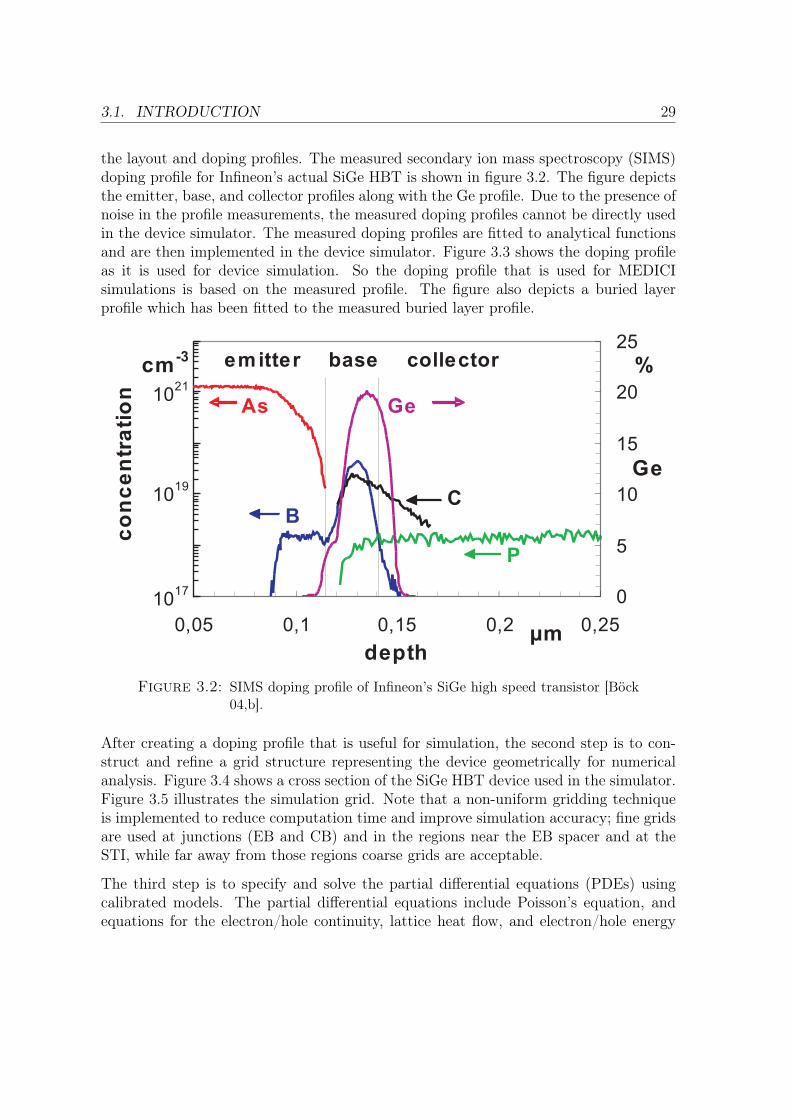
3.1. INTRODUCTION 29
the layout and doping profiles. The measured secondary ion mass spectroscopy (SIMS)doping profile for Infineon’s actual SiGe HBT is shown in figure 3.2. The figure depictsthe emitter, base, and collector profiles along with the Ge profile. Due to the presence ofnoise in the profile measurements, the measured doping profiles cannot be directly usedin the device simulator. The measured doping profiles are fitted to analytical functionsand are then implemented in the device simulator. Figure 3.3 shows the doping profileas it is used for device simulation. So the doping profile that is used for MEDICIsimulations is based on the measured profile. The figure also depicts a buried layerprofile which has been fitted to the measured buried layer profile.
Figure 3.2: SIMS doping profile of Infineon’s SiGe high speed transistor [Böck04,b].
After creating a doping profile that is useful for simulation, the second step is to con-struct and refine a grid structure representing the device geometrically for numericalanalysis. Figure 3.4 shows a cross section of the SiGe HBT device used in the simulator.Figure 3.5 illustrates the simulation grid. Note that a non-uniform gridding techniqueis implemented to reduce computation time and improve simulation accuracy; fine gridsare used at junctions (EB and CB) and in the regions near the EB spacer and at theSTI, while far away from those regions coarse grids are acceptable.
The third step is to specify and solve the partial differential equations (PDEs) usingcalibrated models. The partial differential equations include Poisson’s equation, andequations for the electron/hole continuity, lattice heat flow, and electron/hole energy
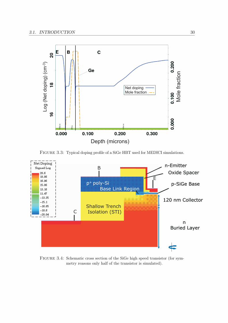
3.1. INTRODUCTION 30
Mole
fraction
Depth (microns)
Net dopingMole fraction
Lo
g(N
et
do
pin
g)
(cm
-3)
Figure 3.3: Typical doping profile of a SiGe HBT used for MEDICI simulations.
p+ poly-Si
Shallow TrenchIsolation (STI)
n-Emitter
nBuried Layer
p-SiGe BaseBase Link Region
Oxide Spacer
C
B
E
120 nm Collector
p+ poly-Si
Shallow TrenchIsolation (STI)
n-Emitter
nBuried Layer
p-SiGe BaseBase Link Region
Oxide Spacer
C
B
E
120 nm Collector
Figure 3.4: Schematic cross section of the SiGe high speed transistor (for sym-metry reasons only half of the transistor is simulated).
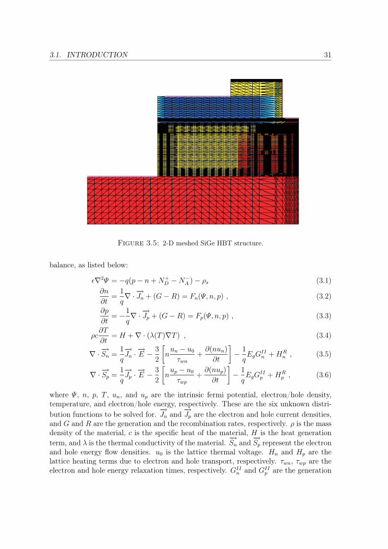
3.1. INTRODUCTION 31
Figure 3.5: 2-D meshed SiGe HBT structure.
balance, as listed below:
ε∇2Ψ = −q(p− n + N+D −N−
A )− ρs (3.1)∂n
∂t=
1
q∇ · −→Jn + (G−R) = Fn(Ψ, n, p) , (3.2)
∂p
∂t= −1
q∇ · −→Jp + (G−R) = Fp(Ψ, n, p) , (3.3)
ρc∂T
∂t= H +∇ · (λ(T )∇T ) , (3.4)
∇ · −→Sn =1
q
−→Jn · −→E − 3
2
[n
un − u0
τwn
+∂(nun)
∂t
]− 1
qEgG
IIn + HR
n , (3.5)
∇ · −→Sp =1
q
−→Jp · −→E − 3
2
[n
up − u0
τwp
+∂(nup)
∂t
]− 1
qEgG
IIp + HR
p , (3.6)
where Ψ , n, p, T , un, and up are the intrinsic fermi potential, electron/hole density,temperature, and electron/hole energy, respectively. These are the six unknown distri-bution functions to be solved for.
−→Jn and
−→Jp are the electron and hole current densities,
and G and R are the generation and the recombination rates, respectively. ρ is the massdensity of the material, c is the specific heat of the material, H is the heat generationterm, and λ is the thermal conductivity of the material.
−→Sn and
−→Sp represent the electron
and hole energy flow densities. u0 is the lattice thermal voltage. Hn and Hp are thelattice heating terms due to electron and hole transport, respectively. τwn, τwp are theelectron and hole energy relaxation times, respectively. GII
n and GIIp are the generation
3.1. INTRODUCTION 32
rates for electron and hole impact ionization, respectively. Fn and Fp are the right handside of the electron and hole current continuity equations, respectively.
First, a solution of the drift-diffusion equations for the classical variables Ψ , n, and p ateach node is obtained using the drift-diffusion approach. MEDICI solves the lattice heatequation in addition to Poisson’s equation and the electron and hole current-continuityequations to obtain the temperature T, at each node. This is followed by a solution ofthe energy balance equations for the electron and hole thermal voltages un and up. Thenew temperature distributions are used to re-evaluate Ψ , n, and p. This procedure isrepeated until the maximum updates of the electron and hole temperature normalizedby the lattice temperature u0 fall below a particular tolerance.
This complicated equation system can be simplified in a lot of practical cases. The moresimplified system used in this work, which is a special case of equations (3.1) - (3.6) isdescribed in more detail in the next sections.
To solve the PDEs on a computer, they are discretized using the generated device grid.The continuous functions of the PDEs are represented by vectors of function values atthe nodes, and the differential operators are replaced by suitable difference operators.Using this discretization technique, MEDICI solves for 6N real values instead of solvingthe six functions, where N is the number of grid points. In MEDICI, the user canturn the models on/off and change model parameters if necessary for simulations. Theresults can then be studied to determine the most effective way to decouple devicephysics effects.
In the same manner as a circuit simulator (e.g. PSPICE, ADS, Spectre), MEDICIoffers dc, ac, and transient analysis. One can mimic the dc, ac, and transient measure-ments in simulations and compare the results with those obtained experimentally. UsingMEDICI, one can modify the process data (such as the doping profile, the Ge content,the device geometry, etc.) and gain insights into the impact of process technology ondevice performance.
A frequent problem in device simulation is the convergency issue, where the PDE solveris unable to obtain a convergent result for the equations. Typical methods to addressthis include:
1. mesh size adjustment, which typically involves a mesh using a finer grid; and
2. model modification, by turning on/off some models or changing model parameters.Once convergence has been achieved, MEDICI saves the solution, and outputs thedc, ac, and transient responses.
MEDICI is an excellent good tool for connecting the device technology, physics, andcharacteristics. Therefore, this tool is applied to the analysis of the high frequency SiGeHBTs in this work.
3.2. SEMICONDUCTOR EQUATIONS FOR HBT’S 33
3.2 Semiconductor Equations for HBT’s
In this section a more simplified version of the general system of PDEs (equations (3.1)- (3.6)) is discussed, as it is used for the simulations in this work. Basic semiconductorequations solved are Poisson’s equation and the carrier continuity equations for electronsand holes. Poisson’s equation relates variations in electrostatic potential to the space-charge density and is given by
ε∇2Ψ = −q(p− n + N+D − N−A)− ρs , (3.7)
where Ψ is the intrinsic fermi potential, ε is the local dielectric permittivity, q is theelementary charge, p and n are the hole and electron concentrations, N+
D and N−
A arethe ionized donor and acceptor impurity concentrations, and ρs is the surface chargedensity.
The continuity equations for electrons and holes relate changes in particle densitiesto the current density and the net recombination rate. The continuity equations forelectrons and holes are written as
∂n
∂t=
1
q∇ · −→Jn + (G−R) , (3.8)
∂p
∂t= −1
q∇ · −→Jp + (G−R) . (3.9)
The above equations provide the general base for device simulation. However, furtheradditional equations are necessary to specify particular physical models for current den-sity, and generation and recombination rates. The current density equations are usuallyobtained by applying approximations and simplifications to the Boltzmann transportequation (BTE), which result in a number of possible transport models such as thedrift-diffusion model [Selberherr 84].
In the drift-diffusion model, the current densities are expressed in terms of quasi-Fermilevels φn and φp as
−→Jn = −qμnn∇φn , (3.10)−→Jp = −qμpp∇φp , (3.11)
where μn and μp are the electron and hole mobilities. Using Boltzmann approximation,the quasi-Fermi levels can be related to the carrier concentrations and the potential asfollows
n = nie exp
[q(Ψ − φn)
kT
], (3.12)
p = nie exp
[−q(Ψ − φp)
kT
], (3.13)
3.2. SEMICONDUCTOR EQUATIONS FOR HBT’S 34
where nie is the effective intrinsic carrier concentration and T is the lattice temperature.Equations (3.10) and (3.11) can be written as
φn = Ψ − kT
qln
n
nie
, (3.14)
φp = Ψ +kT
qln
p
nie
, (3.15)
where Ψ is the intrinsic Fermi potential. Intrinsic Fermi potential Ψ and conductionand valence band edges EC , EV are related to the electrostatic potential φ and can bewritten as follows
Ψ = − 1
2q
(EC + EV − kT ln
NC
NV
), (3.16)
EC = −qφ− χ , (3.17)
EV = −qφ− χ− Eg , (3.18)
where NC and NV are the effective density of states in the conduction and valence band,respectively, and χ is the electron affinity.
By substituting equations (3.14) and (3.15) into equations (3.10) and equation (3.11),we get
−→Jn = qDn∇n− qnμn∇Ψ − μnnkT∇(ln(nie)) , (3.19)−→Jp = −qDp∇p− qnμp∇Ψ − μppkT∇(ln(nie)) , (3.20)
where the last term accounts for the gradient in the effective intrinsic carrier concentra-tion, taking into account bandgap narrowing or heterostructure effects. Effective electricfields are given by
−→En = −∇
(ψ +
kT
qln nie
), (3.21)
−→Ep = −∇
(ψ − kT
qln nie
). (3.22)
From the above and using Einstein’s relationships, the familiar drift-diffusion equationscan be written as follows
−→Jn = qnμn
−→En + qDn∇n , (3.23)
−→Jp = qpμp
−→Ep − qDp∇p , (3.24)
where Dn and Dp are the electron and hole diffusion constants given by kTq
μn and kTq
μp,respectively.
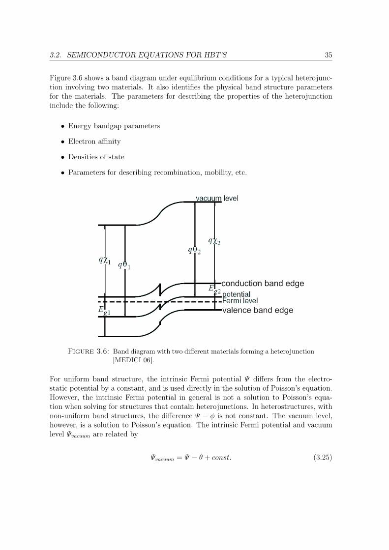
3.2. SEMICONDUCTOR EQUATIONS FOR HBT’S 35
Figure 3.6 shows a band diagram under equilibrium conditions for a typical heterojunc-tion involving two materials. It also identifies the physical band structure parametersfor the materials. The parameters for describing the properties of the heterojunctioninclude the following:
• Energy bandgap parameters
• Electron affinity
• Densities of state
• Parameters for describing recombination, mobility, etc.
conduction band edge
valence band edge
Figure 3.6: Band diagram with two different materials forming a heterojunction[MEDICI 06].
For uniform band structure, the intrinsic Fermi potential Ψ differs from the electro-static potential by a constant, and is used directly in the solution of Poisson’s equation.However, the intrinsic Fermi potential in general is not a solution to Poisson’s equa-tion when solving for structures that contain heterojunctions. In heterostructures, withnon-uniform band structures, the difference Ψ − φ is not constant. The vacuum level,however, is a solution to Poisson’s equation. The intrinsic Fermi potential and vacuumlevel Ψvacuum are related by
Ψvacuum = Ψ − θ + const. (3.25)
3.3. PHYSICAL MODEL SELECTION 36
θ is the band structure parameter given by
θ = χ +Eg
2q+
kT
2qln(
NC
NV
) , (3.26)
where χ is the electron affinity and NC and NV are effective density of states in theconduction band and valence band. If the band structure parameter is spatially constant,then Ψ will be a solution to Poisson’s equation. However, this is not the case withheterojunctions due to differences in band gap, electron affinity, and density of states inadjacent materials. For this reason, Poisson’s equation is written in the following formin MEDICI,
∇ · ε∇(Ψ − θ) = −q(p− n + N+D − N−A)− ρs . (3.27)
The form of the continuity equations remains unchanged for heterojunctions, exceptthat the electric field terms
−→En and
−→Ep in the transport equations must account for
gradients in conduction and valence band edges. Ψ reflects the spatial dependence ofthe intrinsic carrier concentration resulting from the alloyed band structure. The use ofΨ makes it easy to discretize the current continuity equations by assuming reasonablelinearity between mesh points. The five variables, which are Ψ , n, p,
−→Jn, and
−→Jp can then
be solved numerically from the five equations using Scharfetter-Gummel discretizationand Newton’s method [Selberherr 84].
3.3 Physical Model Selection
In solving the semiconductor equations, complex equations and models represent theproperties of the material (e.g. mobility and recombination). Unfortunately, these termsare neither constant nor simple to determine. Typically they are spatially dependentupon the type of material, doping of the material, electron and hole concentrations,electric field, interfaces, etc.. In order to provide accurate simulation results, correctphysical models of these effects must be included in the simulation.
Bipolar devices operate in a wide variety of carrier transport regimes. Majority carriersin the emitter, base, and collector quasi-neutral regions are subjected to ohmic drift.Minority carriers in the emitter can usually be assumed to exhibit pure diffusion. Minor-ity carriers in the base experience a quasi-electric field in the range of several kV/cm,due to doping gradients and/or bandgap variations, which may bring them close tovelocity saturation. Finally, carriers traversing the base-collector depletion region areaccelerated by a strong electric field. Calibration of the physical models used in thiswork were performed for the drift-diffusion approximation. All simulations performedin this work are drift-diffusion simulations. The physical parameters that may needcalibration include majority and minority carrier mobilities, BGN, and Auger and trap-assisted recombination rates. Parameters for the mobility models are essentially taken
3.3. PHYSICAL MODEL SELECTION 37
from literature. Both theoretical and experimental studies suggest that electron mobil-ity in strained Si1−xGex on (111) Si is lower than in bulk silicon, mainly due to alloyscattering, while the effect of strain enhances the hole mobility [Fischetti 96,Bufler 97].The widely accepted Klaassen mobility model is used for both majority and minoritycarriers in the entire device [Klaassen 92,a,Klaassen 92,b]. Also, a bandgap narrowingof 7.4 meV for each percent concentration of Ge is assumed [People 86,b]. The dielectricconstant of Si1−xGex is obtained by linear interpolation between Si and Ge values.
3.3.1 Physical Models
The device simulation tool is mainly used with physical model parameters that havealready been published and widely accepted. Moreover, models can be turned on/offor changed (e.g. by using different models or model parameters) during the simulation.Hence, various device physics effects can be decoupled and the consequences on devicebehavior can be studied. The parameters used in this work are summarized in the table3.1. In a SiGe HBT, the Ge mole fraction is typically a function of position, so both χand Eg vary with position. The most significant material parameter to be specified inthe simulation of SiGe HBTs is the bandgap narrowing induced by incorporation of aGe fraction x. The Ge induced BGN is modelled as [People 86,a]
ΔEg,Ge = 0.74x , (3.28)
where x is the Ge content.
Position-dependent electron affinity χ is modelled as [People 86,a]
χ(x) = χSi + 0.14x− 0.2x2 . (3.29)
In order to account for heavy doping effects on bandgap, the Slotboom BGN model[Slotboom 76] originally developed for Si is used for SiGe. This describes the effectivecarrier concentration ni,eff for heavy doping using a Boltzmann statistics-based equationdespite the presence of degeneracy effects,
n2i,eff = n2
i,0 exp
(ΔEg,app
kT
), (3.30)
n2i,0 = NCNV exp
(ΔEg,0
kT
), (3.31)
where ni,0 is the intrinsic carrier density at moderate doping, NC , NV are the conductionand valence band effective density of states (DOS), ΔEg,0 is the bandgap at moderatedoping, and ΔEg,app is the apparent BGN, which is a function of the doping levelNtotal(x, y), and is modelled as [MEDICI 06].
3.3. PHYSICAL MODEL SELECTION 38
�Eg,app =ΔEg,0
2kT
⌈ln
Ntotal(x, y)
N0+
√ln
N2total(x, y)
N0+ C
⌋, (3.32)
with ΔEg,0 = 6.92 meV, N0 = 7×1017 cm−3, and C = 0.5. The values are taken from[Alamo 87]. The apparent BGN term �Eg,app in equation (3.30) lumps together threedistinct physical phenomena on nie:
• The rigid bandgap shift due to impurity band formation (the Mott transition),
• Degeneracy effects (i.e. the need for Fermi-Dirac statistics to describe high carrierdensities),
• The heavy-doping induced perturbation of the DOS function.
So the BGN approach is a pragmatic way that facilitates the description and modellingof heavily doped bipolar devices with much simpler equations based on Boltzmannstatistics. Complete ionization of dopants in Si (or Ge) is assumed throughout thework. Boltzmann statistics is used in the simulations performed in this work. Thevalues of the parameters used in the simulation are listed in table 3.1.
Boltzmann statistics is used with the BGN model since it is consistent with the BGNdefault parameters. Using FERMI statistics would produce inconsistent results becausethis method accounts for the degeneracy twice, i.e. once using degeneracy parametersand again due to the apparent BGN term [Shi 03],
n2ie(x, y) = n2
i γnγp exp(�Eg) , (3.33)
where γn and γp are factors accounting for degeneracy. For high doping concentrationsthese factors are less than 1 for Fermi statistics and more than 1 for Boltzmann statis-tics, respectively. As a result, MEDICI effectively would take into account the carrierdegeneracy twice, implicitly through the use of apparent BGN and explicitly throughthe use of Fermi-Dirac statistics (γn and γp).
3.3.2 Mobility Models
Electrons and holes in a device are accelerated by electric fields but loose momentumas a result of various scattering processes. These scattering mechanisms include lat-tice vibrations, impurity ions, other carriers, interfaces, and material imperfections. Tosimplify these mechanisms for modelling purposes, mobility is usually defined as a func-tion of lattice temperature, local electric field, and doping concentration. In a devicesimulator, a mobility model is typically further subdivided into
3.3. PHYSICAL MODEL SELECTION 39
• Low-field behavior,
• High-field behavior,
• Bulk semiconductor regions,
• Inversion layers.
In low electric fields, carriers are almost in equilibrium, and mobility is affected bylattice and phonon scattering. Low-field mobility models can be used in this regime.For the simulation of SiGe HBT’s, the philips unified mobility model (PHUMOB) [Klaassen92,a] is selected from the low-field mobility models. It includes acceptor, donor, andcarrier-carrier scattering that can be selected with the PHUMOB parameter in the MODELS
statement. The PHUMOB model takes into account the following:
• Distinct acceptor and donor scattering,
• Carrier-carrier scattering,
• Screening.
It separately models majority and minority carrier mobilities and is appropriate foraddressing bipolar devices.
In high electric fields, mobility decreases due to increased scattering. Eventually, driftvelocity saturates at saturation velocity υsat, which is primarily a function of latticetemperature. The field-dependent mobility model FLDMOB offered by MEDICI [MEDICI06] is used in this work.
3.3.3 Recombination and Carrier Lifetimes
In order to account for the dominant recombination processes in bulk Si, Shockley-Read-Hall (SRH) and Auger recombination models are used in the simulation. Sincethe strained SiGe is similar in band structure to silicon, the same recombination modelis assumed for SiGe [Armstrong 07]. Doping-dependent minority carrier lifetime modelsare used. The assumed minority carrier lifetimes are shorter than in silicon due to alarger number of misfit dislocations. Table 3.1 summarizes the parameters used in thesimulation.
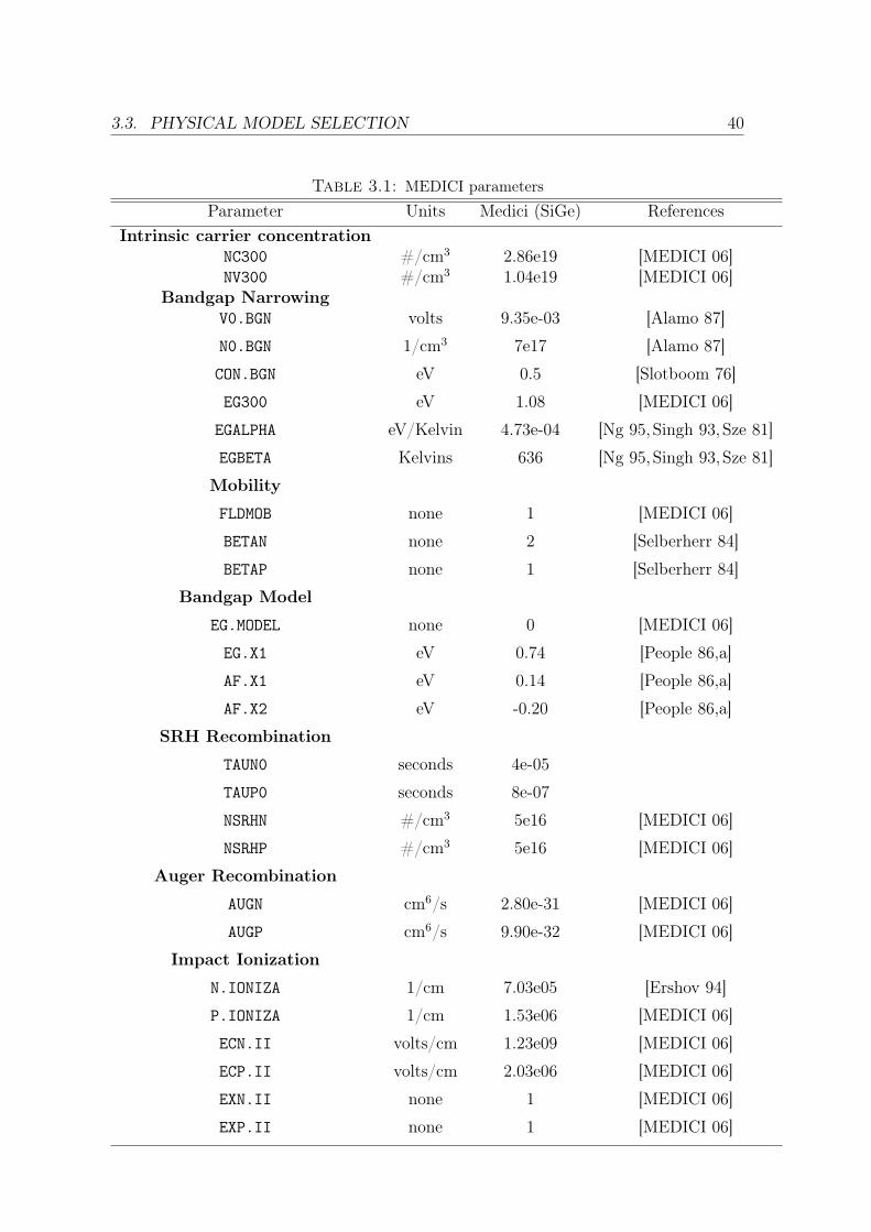
3.3. PHYSICAL MODEL SELECTION 40
Table 3.1: MEDICI parameters
Parameter Units Medici (SiGe) References
Intrinsic carrier concentration
NC300 #/cm3 2.86e19 [MEDICI 06]NV300 #/cm3 1.04e19 [MEDICI 06]
Bandgap Narrowing
V0.BGN volts 9.35e-03 [Alamo 87]
N0.BGN 1/cm3 7e17 [Alamo 87]
CON.BGN eV 0.5 [Slotboom 76]
EG300 eV 1.08 [MEDICI 06]
EGALPHA eV/Kelvin 4.73e-04 [Ng 95,Singh 93,Sze 81]
EGBETA Kelvins 636 [Ng 95,Singh 93,Sze 81]
Mobility
FLDMOB none 1 [MEDICI 06]
BETAN none 2 [Selberherr 84]
BETAP none 1 [Selberherr 84]
Bandgap Model
EG.MODEL none 0 [MEDICI 06]
EG.X1 eV 0.74 [People 86,a]
AF.X1 eV 0.14 [People 86,a]
AF.X2 eV -0.20 [People 86,a]
SRH Recombination
TAUN0 seconds 4e-05
TAUP0 seconds 8e-07
NSRHN #/cm3 5e16 [MEDICI 06]
NSRHP #/cm3 5e16 [MEDICI 06]
Auger Recombination
AUGN cm6/s 2.80e-31 [MEDICI 06]
AUGP cm6/s 9.90e-32 [MEDICI 06]
Impact Ionization
N.IONIZA 1/cm 7.03e05 [Ershov 94]
P.IONIZA 1/cm 1.53e06 [MEDICI 06]
ECN.II volts/cm 1.23e09 [MEDICI 06]
ECP.II volts/cm 2.03e06 [MEDICI 06]
EXN.II none 1 [MEDICI 06]
EXP.II none 1 [MEDICI 06]
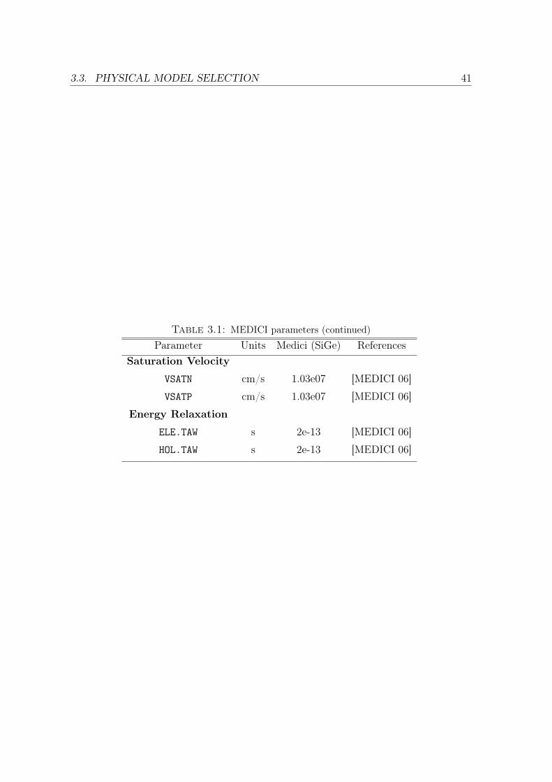
3.3. PHYSICAL MODEL SELECTION 41
Table 3.1: MEDICI parameters (continued)
Parameter Units Medici (SiGe) References
Saturation Velocity
VSATN cm/s 1.03e07 [MEDICI 06]
VSATP cm/s 1.03e07 [MEDICI 06]
Energy Relaxation
ELE.TAW s 2e-13 [MEDICI 06]
HOL.TAW s 2e-13 [MEDICI 06]
Chapter 4
Integration of High Speed Transistors,
High Voltage Transistors, and
Varactors on the Same Chip
This chapter describes a new concept for simultaneous integration of high speed (HS)transistors, high voltage (HV) transistors, and varactors on the same chip. Devicestructure and fabrication process using double epitaxial (DE) concept will be explained.Device simulation results for the HS and HV transistors, and a detailed process anddevice simulation study for the varactors will be presented. Electrical transistor, varac-tor, and circuit results of a voltage-controlled oscillator (VCO) fabricated with the newprocess concept will be discussed.
4.1 Introduction of Double Epitaxy Concept
Advanced high frequency bipolar technologies require devices such as an HV transistorand a varactor in addition to a high speed transistor. Compared to the high speedheterojunction bipolar transistor, the HV transistor has increased base-collector andemitter-collector breakdown voltages. This is necessary for driver stages with high volt-age swings and for ESD protection. Varactors can be used for frequency tuning in VCOs,and are a required part in 77 GHz radar sensors, for automotive distance control. Toimprove the HS transistor’s speed performance, a shallow collector is required to mini-mize the collector delay time. Additionally, doping of the collector has to be increasedin order to reduce the collector resistance and to increase the current density for onsetof the Kirk effect. In the conventional process, this reduction of the collector thicknessdegrades the breakdown voltages of HV transistors as well as the tuning characteristicsof varactors. Therefore, simultaneous optimization of HS, HV transistors, and varactorson the same chip is limited due to the requirement for a shallow collector for the HStransistor.
42
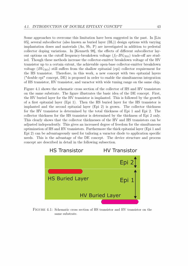
4.1. INTRODUCTION OF DOUBLE EPITAXY CONCEPT 43
Some approaches to overcome this limitation have been suggested in the past. In [Liu05], several subcollector (also known as buried layer (BL)) design options with varyingimplantation doses and materials (As, Sb, P) are investigated in addition to pedestalcollector doping variations. In [Kenneth 98], the effects of different subcollector lay-out options on the cutoff frequency-breakdown voltage (fT -BVCEO) trade-off are stud-ied. Though these methods increase the collector-emitter breakdown voltage of the HVtransistor up to a certain extent, the achievable open-base collector-emitter breakdownvoltage (BVCEO) still suffers from the shallow epitaxial (epi) collector requirement forthe HS transistor. Therefore, in this work, a new concept with two epitaxial layers("double epi" concept, DE) is proposed in order to enable the simultaneous integrationof HS transistor, HV transistor, and varactor with wide tuning range on the same chip.
Figure 4.1 shows the schematic cross section of the collector of HS and HV transistorson the same substrate. The figure illustrates the basic idea of the DE concept. First,the HV buried layer for the HV transistor is implanted. This is followed by the growthof a first epitaxial layer (Epi 1). Then the HS buried layer for the HS transistor isimplanted and the second epitaxial layer (Epi 2) is grown. The collector thicknessfor the HV transistor is determined by the total thickness of Epi 1 and Epi 2. Thecollector thickness for the HS transistor is determined by the thickness of Epi 2 only.This clearly shows that the collector thicknesses of the HV and HS transistors can beadjusted independently. This gives an increased degree of freedom for the simultaneousoptimization of HS and HV transistors. Furthermore the thick epitaxial layer (Epi 1 andEpi 2) can be advantageously used for tailoring a varactor diode to application specificneeds. This is the advantage of the DE concept. The device structure and processconcept are described in detail in the following subsection.
Epi 1
Epi 2
HV Buried Layer
HS Buried Layer
HS Transistor HV Transistor
Figure 4.1: Schematic cross section of HS transistor and HV transistor on thesame substrate.
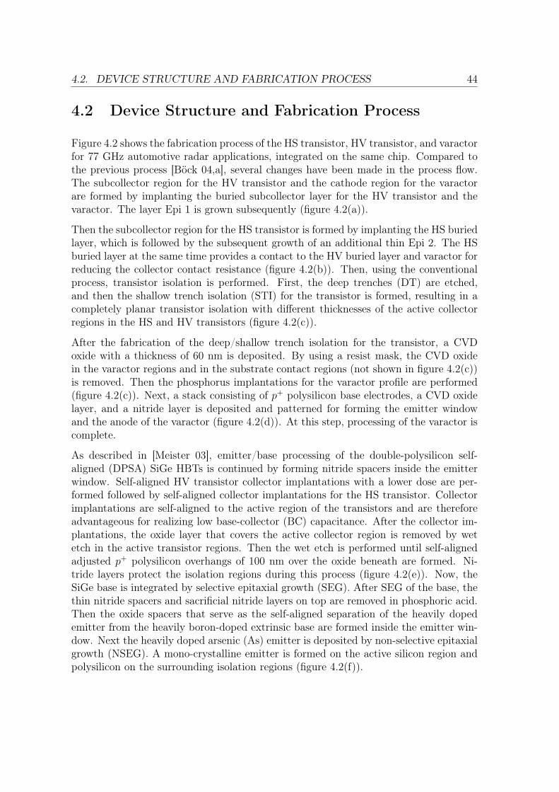
4.2. DEVICE STRUCTURE AND FABRICATION PROCESS 44
4.2 Device Structure and Fabrication Process
Figure 4.2 shows the fabrication process of the HS transistor, HV transistor, and varactorfor 77 GHz automotive radar applications, integrated on the same chip. Compared tothe previous process [Böck 04,a], several changes have been made in the process flow.The subcollector region for the HV transistor and the cathode region for the varactorare formed by implanting the buried subcollector layer for the HV transistor and thevaractor. The layer Epi 1 is grown subsequently (figure 4.2(a)).
Then the subcollector region for the HS transistor is formed by implanting the HS buriedlayer, which is followed by the subsequent growth of an additional thin Epi 2. The HSburied layer at the same time provides a contact to the HV buried layer and varactor forreducing the collector contact resistance (figure 4.2(b)). Then, using the conventionalprocess, transistor isolation is performed. First, the deep trenches (DT) are etched,and then the shallow trench isolation (STI) for the transistor is formed, resulting in acompletely planar transistor isolation with different thicknesses of the active collectorregions in the HS and HV transistors (figure 4.2(c)).
After the fabrication of the deep/shallow trench isolation for the transistor, a CVDoxide with a thickness of 60 nm is deposited. By using a resist mask, the CVD oxidein the varactor regions and in the substrate contact regions (not shown in figure 4.2(c))is removed. Then the phosphorus implantations for the varactor profile are performed(figure 4.2(c)). Next, a stack consisting of p+ polysilicon base electrodes, a CVD oxidelayer, and a nitride layer is deposited and patterned for forming the emitter windowand the anode of the varactor (figure 4.2(d)). At this step, processing of the varactor iscomplete.
As described in [Meister 03], emitter/base processing of the double-polysilicon self-aligned (DPSA) SiGe HBTs is continued by forming nitride spacers inside the emitterwindow. Self-aligned HV transistor collector implantations with a lower dose are per-formed followed by self-aligned collector implantations for the HS transistor. Collectorimplantations are self-aligned to the active region of the transistors and are thereforeadvantageous for realizing low base-collector (BC) capacitance. After the collector im-plantations, the oxide layer that covers the active collector region is removed by wetetch in the active transistor regions. Then the wet etch is performed until self-alignedadjusted p+ polysilicon overhangs of 100 nm over the oxide beneath are formed. Ni-tride layers protect the isolation regions during this process (figure 4.2(e)). Now, theSiGe base is integrated by selective epitaxial growth (SEG). After SEG of the base, thethin nitride spacers and sacrificial nitride layers on top are removed in phosphoric acid.Then the oxide spacers that serve as the self-aligned separation of the heavily dopedemitter from the heavily boron-doped extrinsic base are formed inside the emitter win-dow. Next the heavily doped arsenic (As) emitter is deposited by non-selective epitaxialgrowth (NSEG). A mono-crystalline emitter is formed on the active silicon region andpolysilicon on the surrounding isolation regions (figure 4.2(f)).
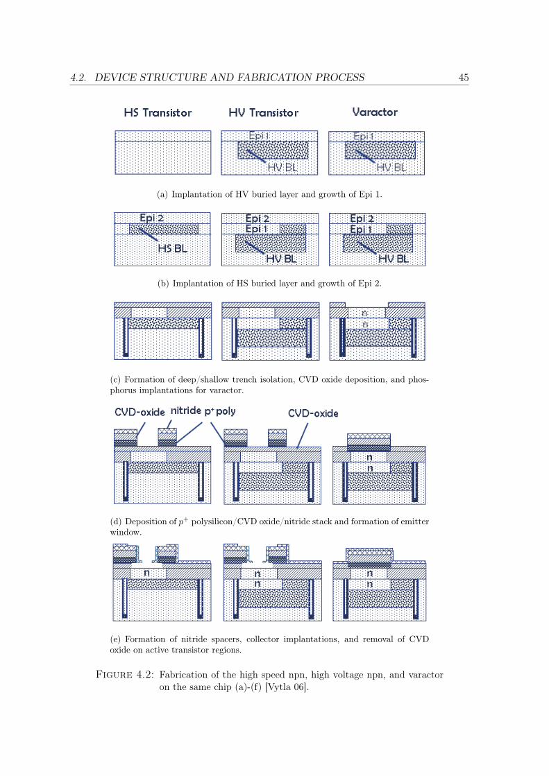
4.2. DEVICE STRUCTURE AND FABRICATION PROCESS 45
(a) Implantation of HV buried layer and growth of Epi 1.
(b) Implantation of HS buried layer and growth of Epi 2.
(c) Formation of deep/shallow trench isolation, CVD oxide deposition, and phos-phorus implantations for varactor.
(d) Deposition of p+ polysilicon/CVD oxide/nitride stack and formation of emitterwindow.
(e) Formation of nitride spacers, collector implantations, and removal of CVDoxide on active transistor regions.
Figure 4.2: Fabrication of the high speed npn, high voltage npn, and varactoron the same chip (a)-(f) [Vytla 06].
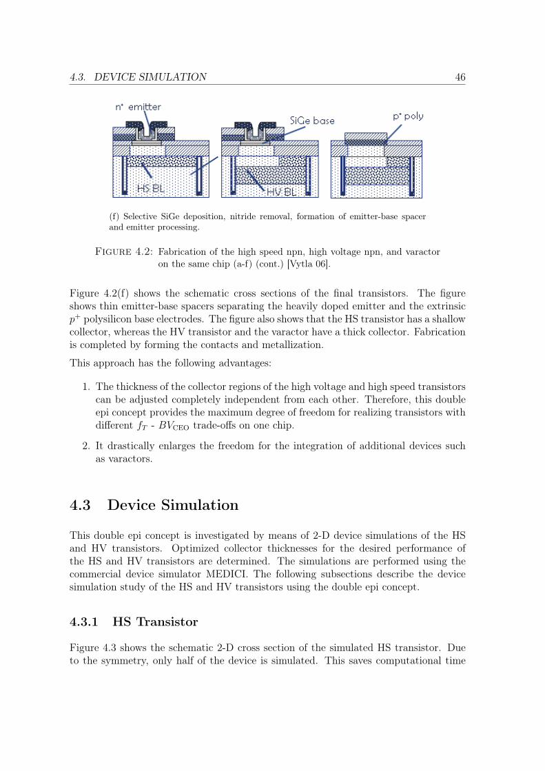
4.3. DEVICE SIMULATION 46
(f) Selective SiGe deposition, nitride removal, formation of emitter-base spacerand emitter processing.
Figure 4.2: Fabrication of the high speed npn, high voltage npn, and varactoron the same chip (a-f) (cont.) [Vytla 06].
Figure 4.2(f) shows the schematic cross sections of the final transistors. The figureshows thin emitter-base spacers separating the heavily doped emitter and the extrinsicp+ polysilicon base electrodes. The figure also shows that the HS transistor has a shallowcollector, whereas the HV transistor and the varactor have a thick collector. Fabricationis completed by forming the contacts and metallization.
This approach has the following advantages:
1. The thickness of the collector regions of the high voltage and high speed transistorscan be adjusted completely independent from each other. Therefore, this doubleepi concept provides the maximum degree of freedom for realizing transistors withdifferent fT - BVCEO trade-offs on one chip.
2. It drastically enlarges the freedom for the integration of additional devices suchas varactors.
4.3 Device Simulation
This double epi concept is investigated by means of 2-D device simulations of the HSand HV transistors. Optimized collector thicknesses for the desired performance ofthe HS and HV transistors are determined. The simulations are performed using thecommercial device simulator MEDICI. The following subsections describe the devicesimulation study of the HS and HV transistors using the double epi concept.
4.3.1 HS Transistor
Figure 4.3 shows the schematic 2-D cross section of the simulated HS transistor. Dueto the symmetry, only half of the device is simulated. This saves computational time
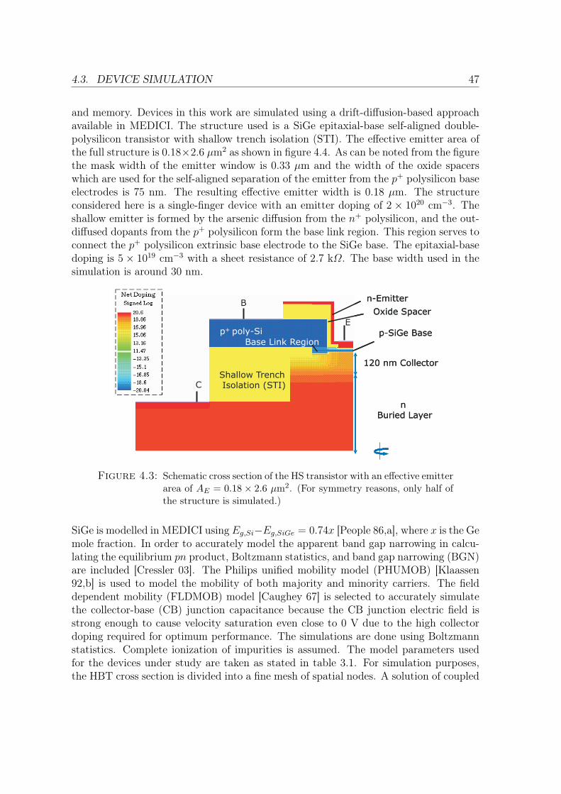
4.3. DEVICE SIMULATION 47
and memory. Devices in this work are simulated using a drift-diffusion-based approachavailable in MEDICI. The structure used is a SiGe epitaxial-base self-aligned double-polysilicon transistor with shallow trench isolation (STI). The effective emitter area ofthe full structure is 0.18×2.6 μm2 as shown in figure 4.4. As can be noted from the figurethe mask width of the emitter window is 0.33 μm and the width of the oxide spacerswhich are used for the self-aligned separation of the emitter from the p+ polysilicon baseelectrodes is 75 nm. The resulting effective emitter width is 0.18 μm. The structureconsidered here is a single-finger device with an emitter doping of 2 × 1020 cm−3. Theshallow emitter is formed by the arsenic diffusion from the n+ polysilicon, and the out-diffused dopants from the p+ polysilicon form the base link region. This region serves toconnect the p+ polysilicon extrinsic base electrode to the SiGe base. The epitaxial-basedoping is 5× 1019 cm−3 with a sheet resistance of 2.7 kΩ. The base width used in thesimulation is around 30 nm.
p+ poly-Si
Shallow TrenchIsolation (STI)
n-Emitter
nBuried Layer
p-SiGe BaseBase Link Region
Oxide Spacer
C
B
E
120 nm Collector
p+ poly-Si
Shallow TrenchIsolation (STI)
n-Emitter
nBuried Layer
p-SiGe BaseBase Link Region
Oxide Spacer
C
B
E
120 nm Collector
Figure 4.3: Schematic cross section of the HS transistor with an effective emitterarea of AE = 0.18 × 2.6 μm2. (For symmetry reasons, only half ofthe structure is simulated.)
SiGe is modelled in MEDICI using Eg,Si−Eg,SiGe = 0.74x [People 86,a], where x is the Gemole fraction. In order to accurately model the apparent band gap narrowing in calcu-lating the equilibrium pn product, Boltzmann statistics, and band gap narrowing (BGN)are included [Cressler 03]. The Philips unified mobility model (PHUMOB) [Klaassen92,b] is used to model the mobility of both majority and minority carriers. The fielddependent mobility (FLDMOB) model [Caughey 67] is selected to accurately simulatethe collector-base (CB) junction capacitance because the CB junction electric field isstrong enough to cause velocity saturation even close to 0 V due to the high collectordoping required for optimum performance. The simulations are done using Boltzmannstatistics. Complete ionization of impurities is assumed. The model parameters usedfor the devices under study are taken as stated in table 3.1. For simulation purposes,the HBT cross section is divided into a fine mesh of spatial nodes. A solution of coupled
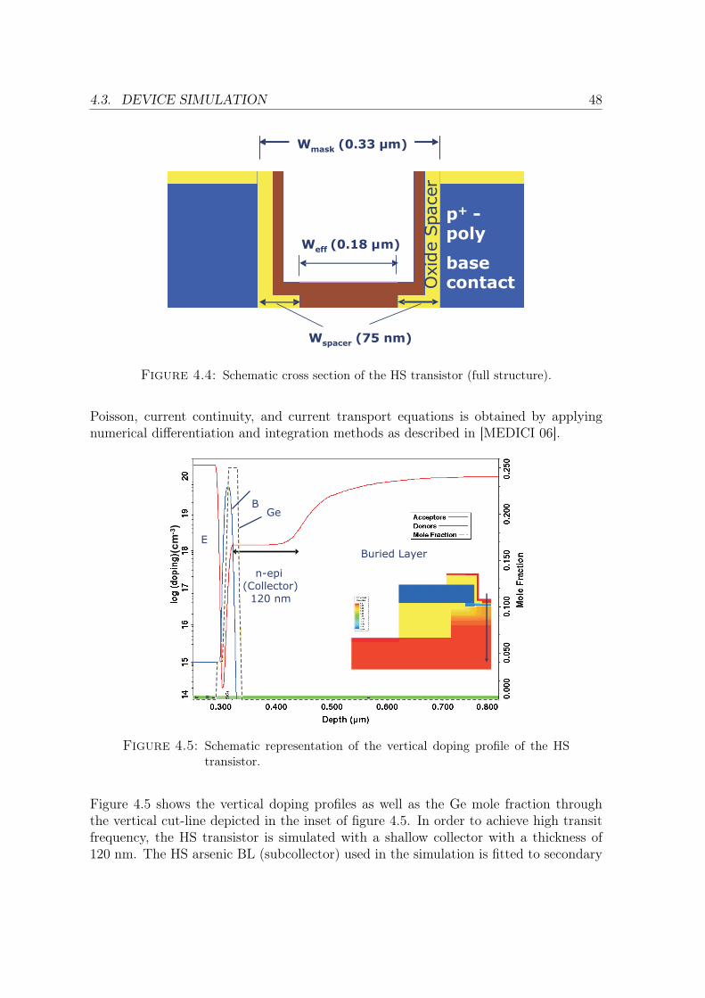
4.3. DEVICE SIMULATION 48
Oxid
eSpacer
p+ -poly
basecontact
Wmask (0.33 μm)
Weff (0.18 μm)
Wspacer (75 nm)
Oxid
eSpacer
p+ -poly
basecontact
Wmask (0.33 μm)
Weff (0.18 μm)
Wspacer (75 nm)
Figure 4.4: Schematic cross section of the HS transistor (full structure).
Poisson, current continuity, and current transport equations is obtained by applyingnumerical differentiation and integration methods as described in [MEDICI 06].
E
BGe
n-epi
(Collector)120 nm
Buried Layer(cm
-3)
E
BGe
n-epi
(Collector)120 nm
Buried Layer
E
BGe
n-epi
(Collector)120 nm
Buried Layer(cm
-3)
Figure 4.5: Schematic representation of the vertical doping profile of the HStransistor.
Figure 4.5 shows the vertical doping profiles as well as the Ge mole fraction throughthe vertical cut-line depicted in the inset of figure 4.5. In order to achieve high transitfrequency, the HS transistor is simulated with a shallow collector with a thickness of120 nm. The HS arsenic BL (subcollector) used in the simulation is fitted to secondary
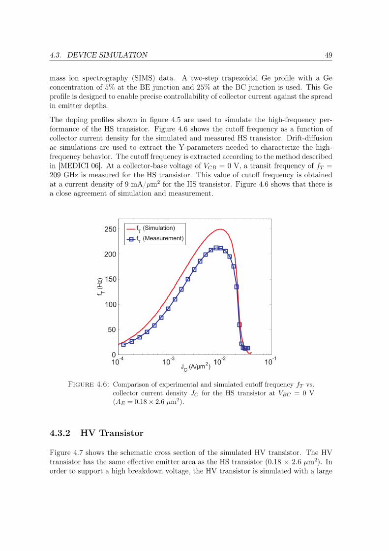
4.3. DEVICE SIMULATION 49
mass ion spectrography (SIMS) data. A two-step trapezoidal Ge profile with a Geconcentration of 5% at the BE junction and 25% at the BC junction is used. This Geprofile is designed to enable precise controllability of collector current against the spreadin emitter depths.
The doping profiles shown in figure 4.5 are used to simulate the high-frequency per-formance of the HS transistor. Figure 4.6 shows the cutoff frequency as a function ofcollector current density for the simulated and measured HS transistor. Drift-diffusionac simulations are used to extract the Y-parameters needed to characterize the high-frequency behavior. The cutoff frequency is extracted according to the method describedin [MEDICI 06]. At a collector-base voltage of VCB = 0 V, a transit frequency of fT =209 GHz is measured for the HS transistor. This value of cutoff frequency is obtainedat a current density of 9 mA/μm2 for the HS transistor. Figure 4.6 shows that there isa close agreement of simulation and measurement.
10-4
10-3
10-2
10-1
0
50
100
150
200
250
JC
(A/μm2)
f T(H
z)
fT
(Simulation)
fT
(Measurement)
Figure 4.6: Comparison of experimental and simulated cutoff frequency fT vs.collector current density JC for the HS transistor at VBC = 0 V(AE = 0.18× 2.6 μm2).
4.3.2 HV Transistor
Figure 4.7 shows the schematic cross section of the simulated HV transistor. The HVtransistor has the same effective emitter area as the HS transistor (0.18 × 2.6 μm2). Inorder to support a high breakdown voltage, the HV transistor is simulated with a large
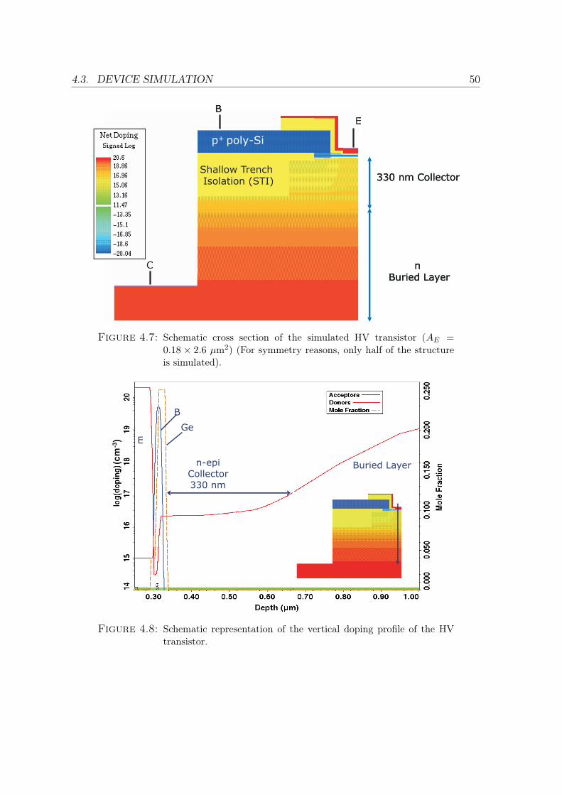
4.3. DEVICE SIMULATION 50
p+ poly-Si
Shallow TrenchIsolation (STI)
C
B
E
nBuried Layer
330 nm Collector
p+ poly-Si
Shallow TrenchIsolation (STI)
C
B
E
nBuried Layer
330 nm Collector
p+ poly-Si
Shallow TrenchIsolation (STI)
C
B
E
nBuried Layer
330 nm Collector
Figure 4.7: Schematic cross section of the simulated HV transistor (AE =
0.18 × 2.6 μm2) (For symmetry reasons, only half of the structureis simulated).
(cm
-3)
n-epiCollector
330 nm
E
B
Ge
(cm
-3)
n-epiCollector
330 nm
E
B
Ge
Buried Layer
Figure 4.8: Schematic representation of the vertical doping profile of the HVtransistor.
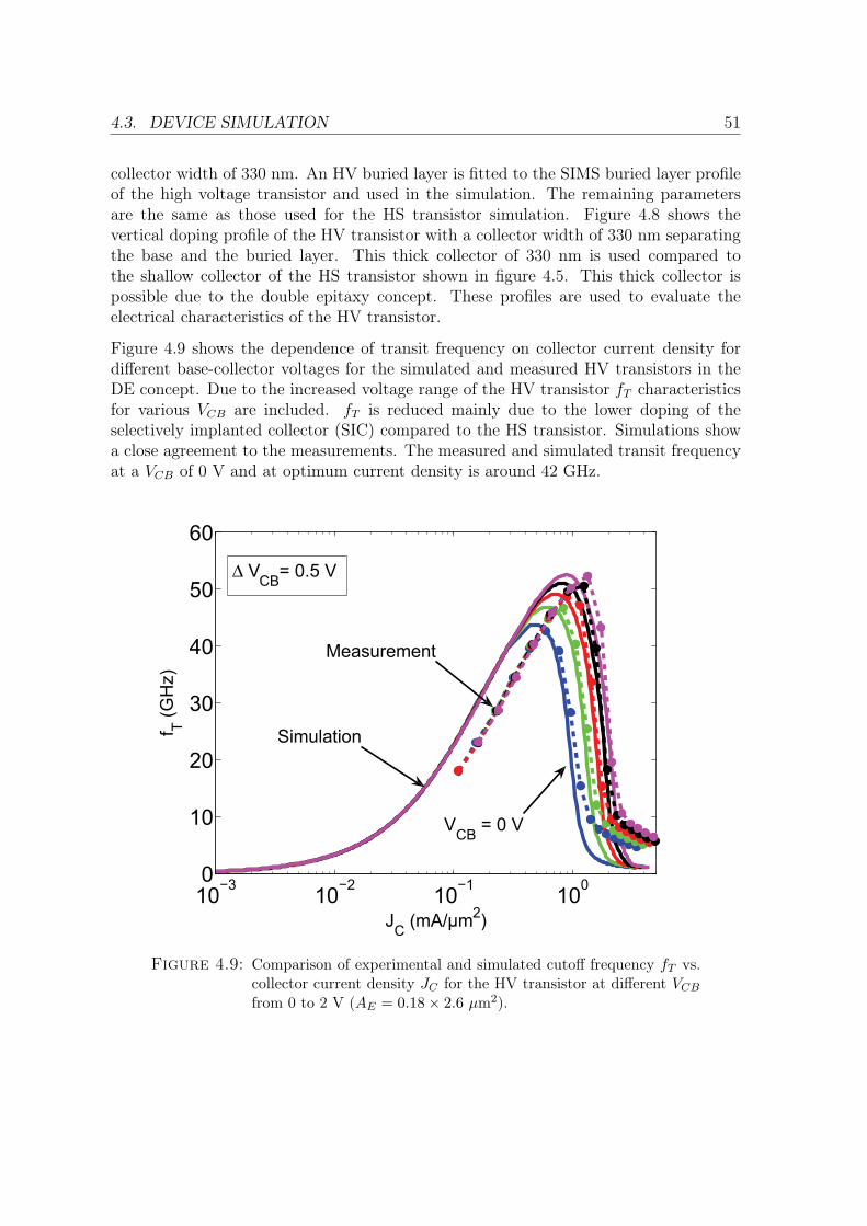
4.3. DEVICE SIMULATION 51
collector width of 330 nm. An HV buried layer is fitted to the SIMS buried layer profileof the high voltage transistor and used in the simulation. The remaining parametersare the same as those used for the HS transistor simulation. Figure 4.8 shows thevertical doping profile of the HV transistor with a collector width of 330 nm separatingthe base and the buried layer. This thick collector of 330 nm is used compared tothe shallow collector of the HS transistor shown in figure 4.5. This thick collector ispossible due to the double epitaxy concept. These profiles are used to evaluate theelectrical characteristics of the HV transistor.
Figure 4.9 shows the dependence of transit frequency on collector current density fordifferent base-collector voltages for the simulated and measured HV transistors in theDE concept. Due to the increased voltage range of the HV transistor fT characteristicsfor various VCB are included. fT is reduced mainly due to the lower doping of theselectively implanted collector (SIC) compared to the HS transistor. Simulations showa close agreement to the measurements. The measured and simulated transit frequencyat a VCB of 0 V and at optimum current density is around 42 GHz.
10−3 10−2 10−1 1000
10
20
30
40
50
60
JC (mA/µm2)
f T (GH
z)
Simulation
Measurement
VCB = 0 V
Δ VCB= 0.5 V
Figure 4.9: Comparison of experimental and simulated cutoff frequency fT vs.collector current density JC for the HV transistor at different VCB
from 0 to 2 V (AE = 0.18× 2.6 μm2).
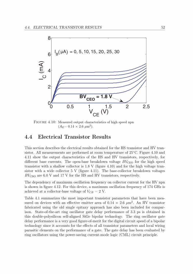
4.4. ELECTRICAL TRANSISTOR RESULTS 52
( )
Figure 4.10: Measured output characteristics of high speed npn(AE= 0.14 × 2.6 μm2).
4.4 Electrical Transistor Results
This section describes the electrical results obtained for the HS transistor and HV tran-sistor. All measurements are performed at room temperature of 25◦C. Figure 4.10 and4.11 show the output characteristics of the HS and HV transistors, respectively, fordifferent base currents. The open-base breakdown voltage BVCEO for the high speedtransistor with a shallow collector is 1.8 V (figure 4.10) and for the high voltage tran-sistor with a wide collector 5 V (figure 4.11). The base-collector breakdown voltagesBVCBO are 6.0 V and 17 V for the HS and HV transistors, respectively.
The dependency of maximum oscillation frequency on collector current for the HV npnis shown in figure 4.12. For this device, a maximum oscillation frequency of 174 GHz isachieved at a collector-base voltage of VCB = 2 V.
Table 4.1 summarizes the most important transistor parameters that have been mea-sured on devices with an effective emitter area of 0.14 × 2.6 μm2. An HV transistorfabricated using the old single epitaxy approach has also been included for compar-ison. State-of-the-art ring oscillator gate delay performance of 3.3 ps is obtained inthis double-polysilicon self-aligned SiGe bipolar technology. The ring oscillator gatedelay performance is a very good figure-of-merit for the digital circuit speed of a bipolartechnology since it accounts for the effects of all transistor parameters and local wiringparasitic elements on the performance of a gate. The gate delay has been evaluated byring oscillators using the power-saving current-mode logic (CML) circuit principle.
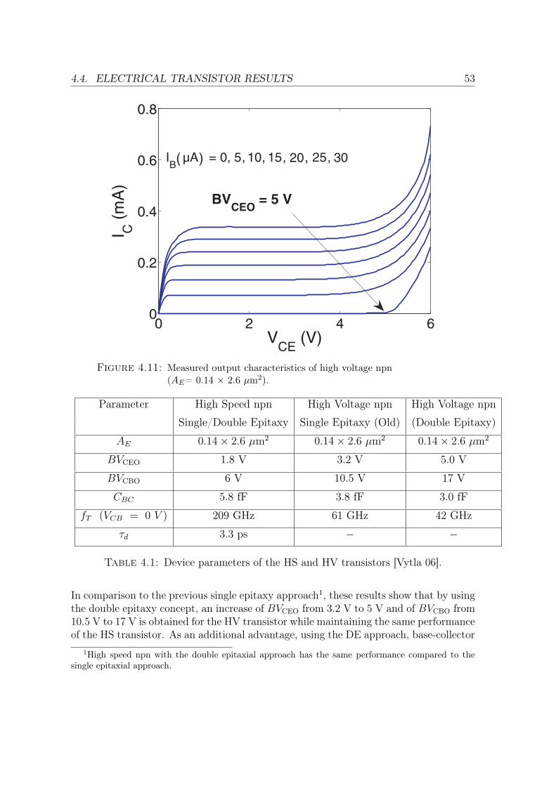
4.4. ELECTRICAL TRANSISTOR RESULTS 53
( )
Figure 4.11: Measured output characteristics of high voltage npn(AE= 0.14 × 2.6 μm2).
Parameter High Speed npn High Voltage npn High Voltage npn
Single/Double Epitaxy Single Epitaxy (Old) (Double Epitaxy)
AE 0.14× 2.6 μm2 0.14× 2.6 μm2 0.14× 2.6 μm2
BVCEO 1.8 V 3.2 V 5.0 V
BVCBO 6 V 10.5 V 17 V
CBC 5.8 fF 3.8 fF 3.0 fF
fT (VCB = 0 V ) 209 GHz 61 GHz 42 GHz
τd 3.3 ps − −
Table 4.1: Device parameters of the HS and HV transistors [Vytla 06].
In comparison to the previous single epitaxy approach1, these results show that by usingthe double epitaxy concept, an increase of BVCEO from 3.2 V to 5 V and of BVCBO from10.5 V to 17 V is obtained for the HV transistor while maintaining the same performanceof the HS transistor. As an additional advantage, using the DE approach, base-collector
1High speed npn with the double epitaxial approach has the same performance compared to thesingle epitaxial approach.
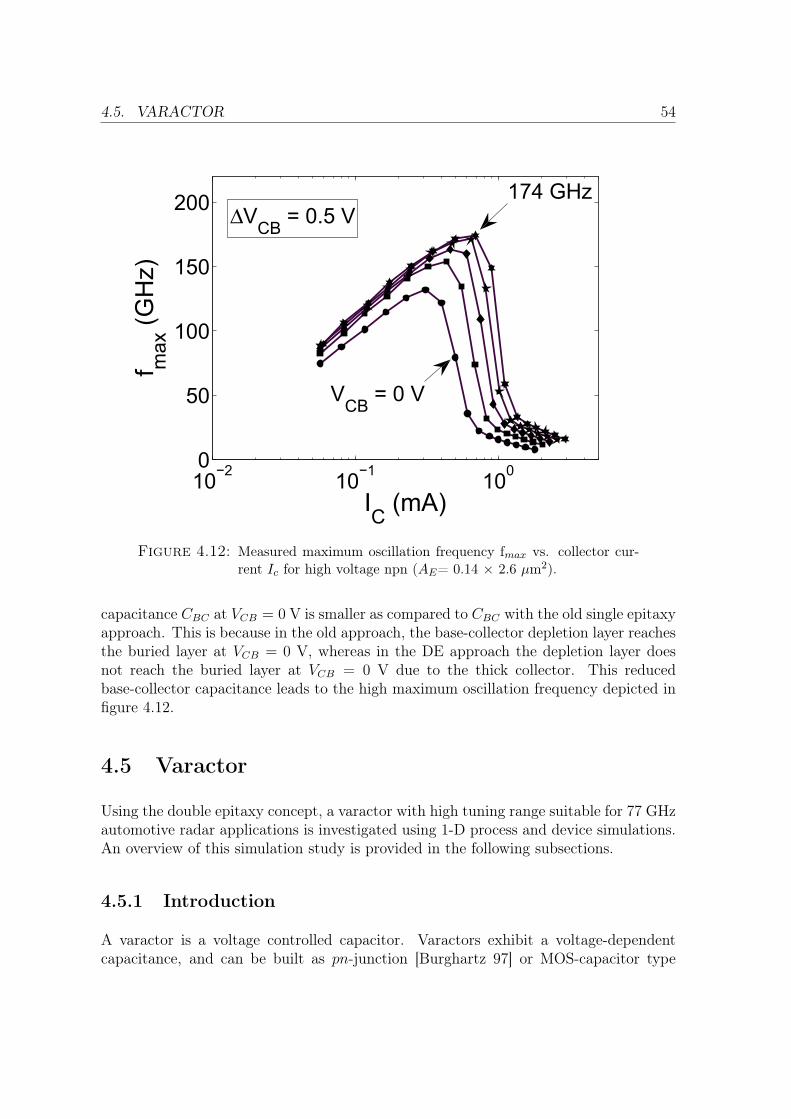
4.5. VARACTOR 54
10−2 10−1 1000
50
100
150
200
IC (mA)
f max
(GH
z)
174 GHz
VCB = 0 V
ΔVCB = 0.5 V
Figure 4.12: Measured maximum oscillation frequency fmax vs. collector cur-rent Ic for high voltage npn (AE= 0.14 × 2.6 μm2).
capacitance CBC at VCB = 0 V is smaller as compared to CBC with the old single epitaxyapproach. This is because in the old approach, the base-collector depletion layer reachesthe buried layer at VCB = 0 V, whereas in the DE approach the depletion layer doesnot reach the buried layer at VCB = 0 V due to the thick collector. This reducedbase-collector capacitance leads to the high maximum oscillation frequency depicted infigure 4.12.
4.5 Varactor
Using the double epitaxy concept, a varactor with high tuning range suitable for 77 GHzautomotive radar applications is investigated using 1-D process and device simulations.An overview of this simulation study is provided in the following subsections.
4.5.1 Introduction
A varactor is a voltage controlled capacitor. Varactors exhibit a voltage-dependentcapacitance, and can be built as pn-junction [Burghartz 97] or MOS-capacitor type
4.5. VARACTOR 55
components [Wong 00]. One important application of varactors is voltage-variable fre-quency tuning [Penfield 62]. The two most important figures-of-merit for characterizingthe varactor performance are capacitance tuning ratio TR and quality factor Q.
Capacitance tuning ratio TR can be considered the most important parameter re-garding the varactor functionality. The tuning range of the capacitance of a specificvaractor is defined as the ratio between maximum capacitance Cmax and minimumcapacitance Cmin. This is given by
TR =Cmax
Cmin
=Capacitance at low reverse bias
Capacitance at high reverse bias. (4.1)
Quality factor Q is the ratio between both stored and lost energy. At high frequencies,this can be written as [Sze 81]
Q =
[1
2πfRs(V )Cj(V )
], (4.2)
where f is the frequency, Rs is the series resistance, and Cj is the junction capac-itance.
A varactor integrated on the same substrate can be used to realize a monolithic voltage-controlled oscillator (VCO), since changing the varactor capacitance changes the fre-quency of oscillation of the VCO within a certain range. For example, VCOs are usedin applications such as radar for automobiles in the frequency band from 76-81 GHz.A transmission signal for such a radar is generated by the VCO. For the practical re-alization of such an application, a VCO tuning range of around 12 GHz is required.This is necessary to cover the system bandwidth and to compensate for process andtemperature variations. It is not possible to achieve such a wide tuning range witha varactor realized in the conventional approach with a single epitaxial layer. This isbecause today’s SiGe HBTs with cutoff frequencies of 200 GHz (or more) require col-lector widths (distance between the pn-junction and the n+ BL) of only 120 nm orless. The resulting collector width limits the realization of a varactor with a sufficientlyhigh Cmax/Cmin ratio, which determines the tuning range of the VCO. The practicalrealization of such a radar requires the integration of a varactor with wide tuning range(a high Cmax/Cmin ratio) and high Q on the same substrate along with transistors withhigh transit frequency, typically 200 GHz or above. In order to achieve high Cmax/Cmin
ratio, the distance of the pn-junction from the n+ BL in the varactor has to be in-creased, and in order to achieve a high transit frequency, a shallow collector width isrequired. These requirements can be met using the DE concept. Figure 4.13 shows theschematic cross section of the varactor and HS transistor integrated on the same sub-strate using the DE concept. As depicted in this figure the HS transistor has a shallowcollector for achieving higher speed, whereas the varactor has a wider epitaxial layerfor achieving a high Cmax/Cmin ratio. Moreover, the characteristics of the varactor and
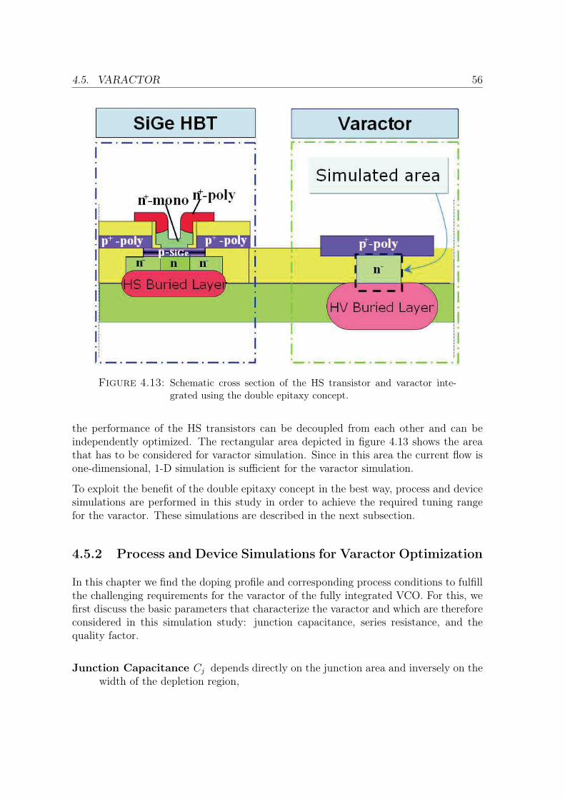
4.5. VARACTOR 56
Figure 4.13: Schematic cross section of the HS transistor and varactor inte-grated using the double epitaxy concept.
the performance of the HS transistors can be decoupled from each other and can beindependently optimized. The rectangular area depicted in figure 4.13 shows the areathat has to be considered for varactor simulation. Since in this area the current flow isone-dimensional, 1-D simulation is sufficient for the varactor simulation.
To exploit the benefit of the double epitaxy concept in the best way, process and devicesimulations are performed in this study in order to achieve the required tuning rangefor the varactor. These simulations are described in the next subsection.
4.5.2 Process and Device Simulations for Varactor Optimization
In this chapter we find the doping profile and corresponding process conditions to fulfillthe challenging requirements for the varactor of the fully integrated VCO. For this, wefirst discuss the basic parameters that characterize the varactor and which are thereforeconsidered in this simulation study: junction capacitance, series resistance, and thequality factor.
Junction Capacitance Cj depends directly on the junction area and inversely on thewidth of the depletion region,
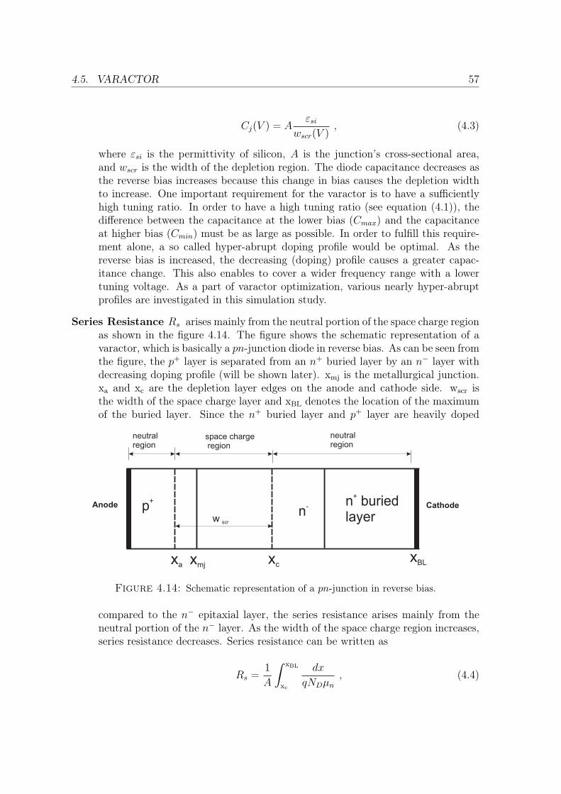
4.5. VARACTOR 57
Cj(V ) = Aεsi
wscr(V ), (4.3)
where εsi is the permittivity of silicon, A is the junction’s cross-sectional area,and wscr is the width of the depletion region. The diode capacitance decreases asthe reverse bias increases because this change in bias causes the depletion widthto increase. One important requirement for the varactor is to have a sufficientlyhigh tuning ratio. In order to have a high tuning ratio (see equation (4.1)), thedifference between the capacitance at the lower bias (Cmax) and the capacitanceat higher bias (Cmin) must be as large as possible. In order to fulfill this require-ment alone, a so called hyper-abrupt doping profile would be optimal. As thereverse bias is increased, the decreasing (doping) profile causes a greater capac-itance change. This also enables to cover a wider frequency range with a lowertuning voltage. As a part of varactor optimization, various nearly hyper-abruptprofiles are investigated in this simulation study.
Series Resistance Rs arises mainly from the neutral portion of the space charge regionas shown in the figure 4.14. The figure shows the schematic representation of avaractor, which is basically a pn-junction diode in reverse bias. As can be seen fromthe figure, the p+ layer is separated from an n+ buried layer by an n− layer withdecreasing doping profile (will be shown later). xmj is the metallurgical junction.xa and xc are the depletion layer edges on the anode and cathode side. wscr isthe width of the space charge layer and xBL denotes the location of the maximumof the buried layer. Since the n+ buried layer and p+ layer are heavily doped
space chargeregion
neutralregion
neutralregion
p+
n- n buried
layer
+
Anode Cathode
xmj xcxa
w scr
xBL
Figure 4.14: Schematic representation of a pn-junction in reverse bias.
compared to the n− epitaxial layer, the series resistance arises mainly from theneutral portion of the n− layer. As the width of the space charge region increases,series resistance decreases. Series resistance can be written as
Rs =1
A
∫ xBL
xc
dx
qNDμn
, (4.4)
4.5. VARACTOR 58
where A is the area of the junction, q is the elementary charge, ND is the donordoping concentration, and μn is the electron mobility. Rs is a very importantparameter which needs to be optimized, because it is related to the quality factoras shown in equation (4.2).
Quality Factor Q is very important for the phase noise performance of a VCO. It isnecessary to have low phase noise which finally determines system parameters likethe spatial resolution of a radar system. In order to have high Q and low phasenoise, Rs needs to be reduced. Investigations for achieving high Q by using variousRs optimizations are performed.
Figure 4.15 gives a block diagram showing the steps involved in varactor process anddevice simulation. Figure 4.16 shows the flow chart for the simulation procedure thatis performed for varactor optimization.
Each of the blocks depicted in figure 4.15 is described below.
Process Simulation: 1-D process simulations for the varactor are performed with theprocess simulator TSUPREM4. Process simulation steps are illustrated in figure4.17. First a thin (10 nm) thermal oxide is grown (figure 4.17(a)). Then, theHV buried layer that serves as a cathode region is implanted with a dose of 5 ×1015 cm−2 and implantation energy of 40 keV on a p-substrate with a resistivity of20 Ωcm (figure 4.17(b)). The implantation damage caused by the BL implantationis annealed at a temperature of 1100oC for 5 seconds. The BL diffuses verticallydue to this annealing step (figure 4.17(c)). Then, a thick epitaxial layer (the thick-ness of the epitaxial layer is the sum of the thicknesses of Epi 1 and Epi 2 of section4.2) is deposited (figure 4.17(d)). Afterwards multiple phosphorus implantationswith different doses and energies for the varactor are performed (figure 4.17(e)).How these implantations are chosen to achieve a hyper-abrupt like profile with ahigh tuning ratio and a low series resistance is described later. The implantationdamage caused by the phosphorus implantations is annealed at a temperature of1000oC for 10 seconds. During this step, the HV buried layer is further diffused(figure 4.17(f)). The final epitaxial thickness for the varactor is the distance fromthe surface of the chip in figure 4.17(f) to the BL. For the calculation of implan-tation doses and energy not only tuning ratio and series resistance is considered,but it is also taken care that the final profile is robust against process variations.
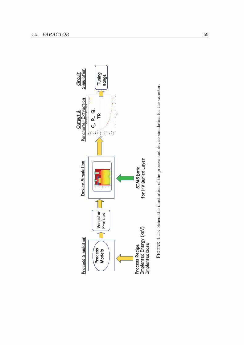
4.5. VARACTOR 59
E
R
D
DB
C,R
,Q
,
TR
js
L
Fig
ure
4.1
5:
Sch
emat
icillu
stra
tion
ofth
epro
cess
and
dev
ice
sim
ula
tion
for
the
vara
ctor
.
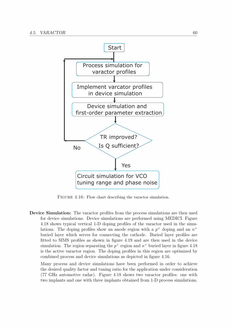
4.5. VARACTOR 60
Is Q sufficient?
TR improved?
Circuit simulation for VCO
tuning range and phase noise
Process simulation for
varactor profiles
Implement varcator profiles
in device simulation
Device simulation and
first-order parameter extraction
Start
No
Yes
Figure 4.16: Flow chart describing the varactor simulation.
Device Simulation: The varactor profiles from the process simulations are then usedfor device simulations. Device simulations are performed using MEDICI. Figure4.18 shows typical vertical 1-D doping profiles of the varactor used in the simu-lations. The doping profiles show an anode region with a p+ doping and an n+
buried layer which serves for connecting the cathode. Buried layer profiles arefitted to SIMS profiles as shown in figure 4.19 and are then used in the devicesimulation. The region separating the p+ region and n+ buried layer in figure 4.18is the active varactor region. The doping profiles in this region are optimized bycombined process and device simulations as depicted in figure 4.16.
Many process and device simulations have been performed in order to achievethe desired quality factor and tuning ratio for the application under consideration(77 GHz automotive radar). Figure 4.18 shows two varactor profiles: one withtwo implants and one with three implants obtained from 1-D process simulations.
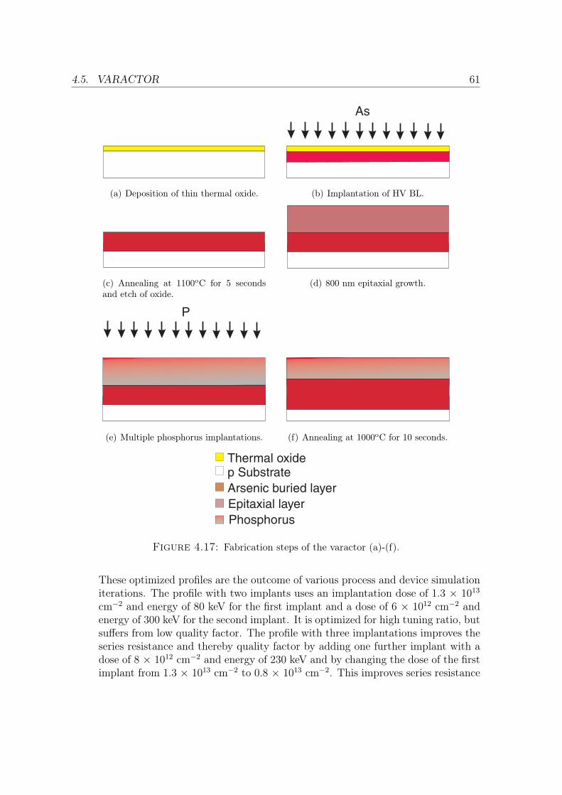
4.5. VARACTOR 61
(a) Deposition of thin thermal oxide.
As
(b) Implantation of HV BL.
(c) Annealing at 1100oC for 5 secondsand etch of oxide.
(d) 800 nm epitaxial growth.
P
(e) Multiple phosphorus implantations. (f) Annealing at 1000oC for 10 seconds.
p SubstrateThermal oxide
Arsenic buried layerEpitaxial layerPhosphorus
Figure 4.17: Fabrication steps of the varactor (a)-(f).
These optimized profiles are the outcome of various process and device simulationiterations. The profile with two implants uses an implantation dose of 1.3 × 10¹³
cm−2 and energy of 80 keV for the first implant and a dose of 6 × 1012 cm−2 andenergy of 300 keV for the second implant. It is optimized for high tuning ratio, butsuffers from low quality factor. The profile with three implantations improves theseries resistance and thereby quality factor by adding one further implant with adose of 8 × 1012 cm−2 and energy of 230 keV and by changing the dose of the firstimplant from 1.3 × 1013 cm−2 to 0.8 × 1013 cm−2. This improves series resistance
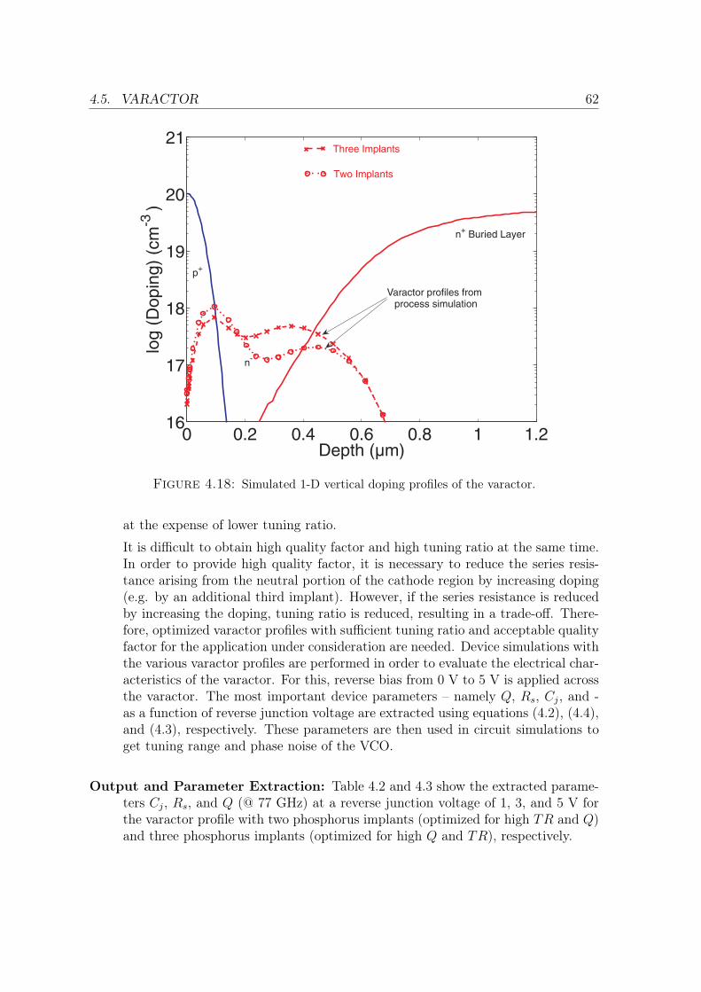
4.5. VARACTOR 62
0 0.2 0.4 0.6 0.8 1 1.216
17
18
19
20
21
Depth ( )μm
log
(Do
pin
g)
(cm
-3)
p+
n+
Buried Layer
Varactor profiles fromprocess simulation
n-
Three Implants
Two Implants
Figure 4.18: Simulated 1-D vertical doping profiles of the varactor.
at the expense of lower tuning ratio.
It is difficult to obtain high quality factor and high tuning ratio at the same time.In order to provide high quality factor, it is necessary to reduce the series resis-tance arising from the neutral portion of the cathode region by increasing doping(e.g. by an additional third implant). However, if the series resistance is reducedby increasing the doping, tuning ratio is reduced, resulting in a trade-off. There-fore, optimized varactor profiles with sufficient tuning ratio and acceptable qualityfactor for the application under consideration are needed. Device simulations withthe various varactor profiles are performed in order to evaluate the electrical char-acteristics of the varactor. For this, reverse bias from 0 V to 5 V is applied acrossthe varactor. The most important device parameters – namely Q, Rs, Cj, and -as a function of reverse junction voltage are extracted using equations (4.2), (4.4),and (4.3), respectively. These parameters are then used in circuit simulations toget tuning range and phase noise of the VCO.
Output and Parameter Extraction: Table 4.2 and 4.3 show the extracted parame-ters Cj, Rs, and Q (@ 77 GHz) at a reverse junction voltage of 1, 3, and 5 V forthe varactor profile with two phosphorus implants (optimized for high TR and Q)and three phosphorus implants (optimized for high Q and TR), respectively.
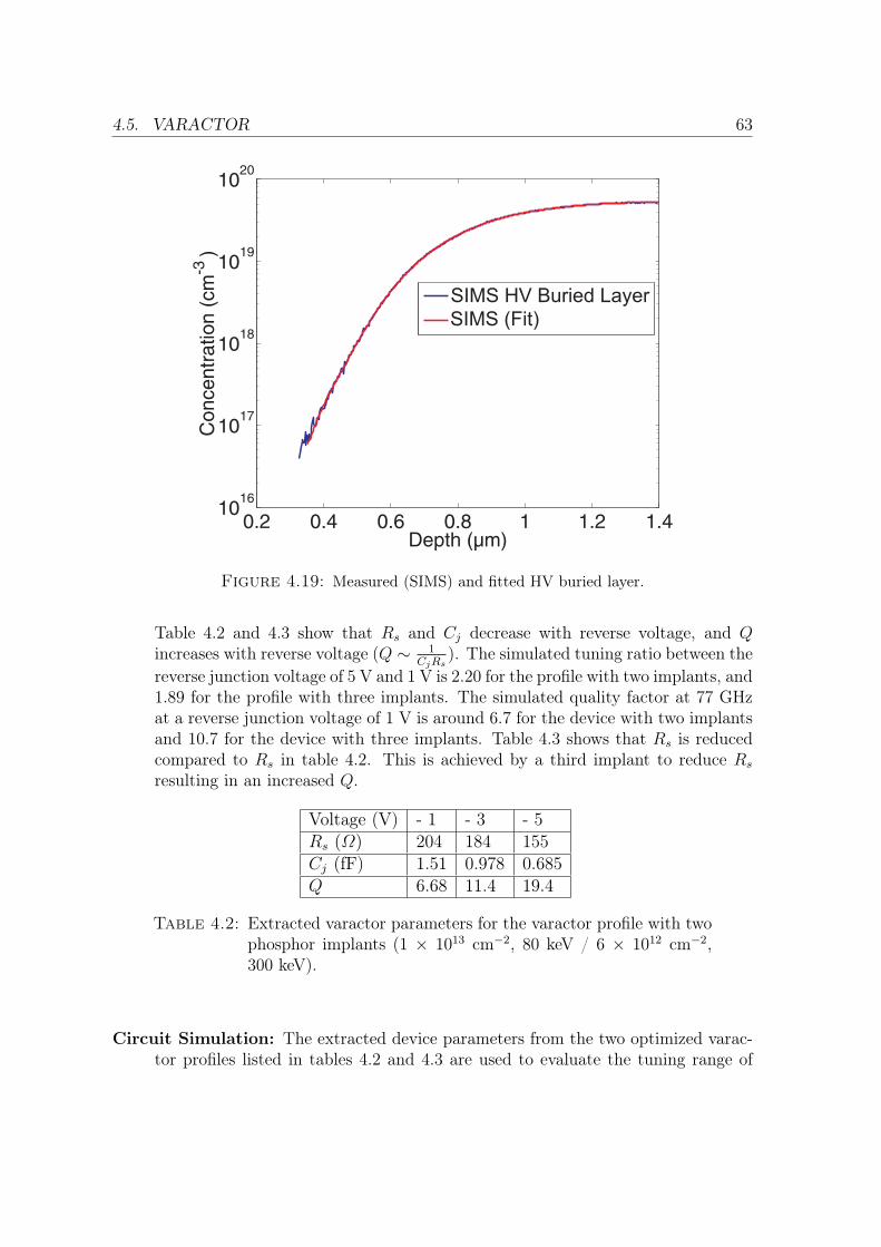
4.5. VARACTOR 63
SIMS HV Buried Layer
SIMS (Fit)
Figure 4.19: Measured (SIMS) and fitted HV buried layer.
Table 4.2 and 4.3 show that Rs and Cj decrease with reverse voltage, and Qincreases with reverse voltage (Q ∼ 1
CjRs). The simulated tuning ratio between the
reverse junction voltage of 5 V and 1 V is 2.20 for the profile with two implants, and1.89 for the profile with three implants. The simulated quality factor at 77 GHzat a reverse junction voltage of 1 V is around 6.7 for the device with two implantsand 10.7 for the device with three implants. Table 4.3 shows that Rs is reducedcompared to Rs in table 4.2. This is achieved by a third implant to reduce Rs
resulting in an increased Q.
Voltage (V) - 1 - 3 - 5Rs (Ω) 204 184 155Cj (fF) 1.51 0.978 0.685Q 6.68 11.4 19.4
Table 4.2: Extracted varactor parameters for the varactor profile with twophosphor implants (1 × 1013 cm−2, 80 keV / 6 × 1012 cm−2,300 keV).
Circuit Simulation: The extracted device parameters from the two optimized varac-tor profiles listed in tables 4.2 and 4.3 are used to evaluate the tuning range of
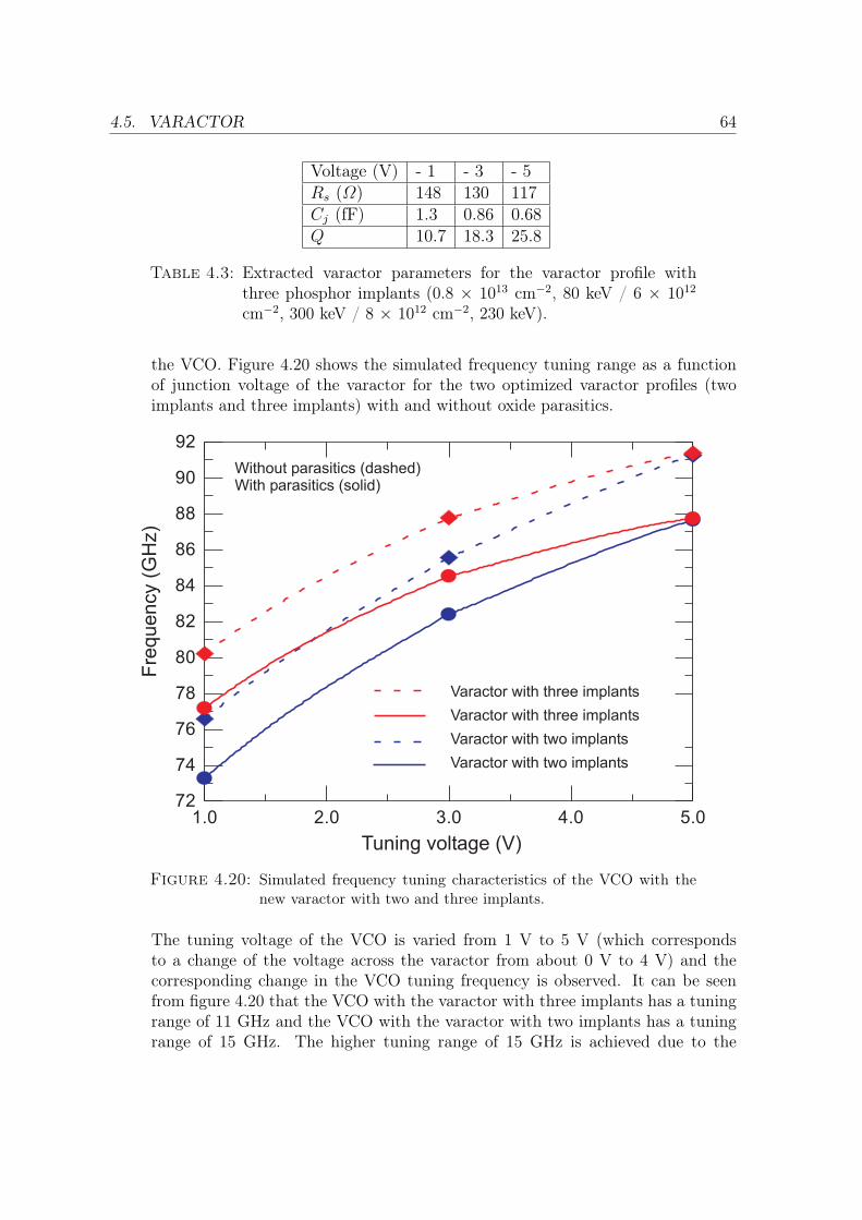
4.5. VARACTOR 64
Voltage (V) - 1 - 3 - 5Rs (Ω) 148 130 117Cj (fF) 1.3 0.86 0.68Q 10.7 18.3 25.8
Table 4.3: Extracted varactor parameters for the varactor profile withthree phosphor implants (0.8 × 1013 cm−2, 80 keV / 6 × 10¹²
cm−2, 300 keV / 8 × 1012 cm−2, 230 keV).
the VCO. Figure 4.20 shows the simulated frequency tuning range as a functionof junction voltage of the varactor for the two optimized varactor profiles (twoimplants and three implants) with and without oxide parasitics.
1.0 2.0 3.0 4.0 5.072
74
76
78
80
82
84
86
88
90
92
Varactor with three implants
Varactor with three implants
Varactor with two implants
Varactor with two implants
Without parasitics (dashed)With parasitics (solid)
Tuning voltage (V)
Fre
quency
(GH
z)
Figure 4.20: Simulated frequency tuning characteristics of the VCO with thenew varactor with two and three implants.
The tuning voltage of the VCO is varied from 1 V to 5 V (which correspondsto a change of the voltage across the varactor from about 0 V to 4 V) and thecorresponding change in the VCO tuning frequency is observed. It can be seenfrom figure 4.20 that the VCO with the varactor with three implants has a tuningrange of 11 GHz and the VCO with the varactor with two implants has a tuningrange of 15 GHz. The higher tuning range of 15 GHz is achieved due to the
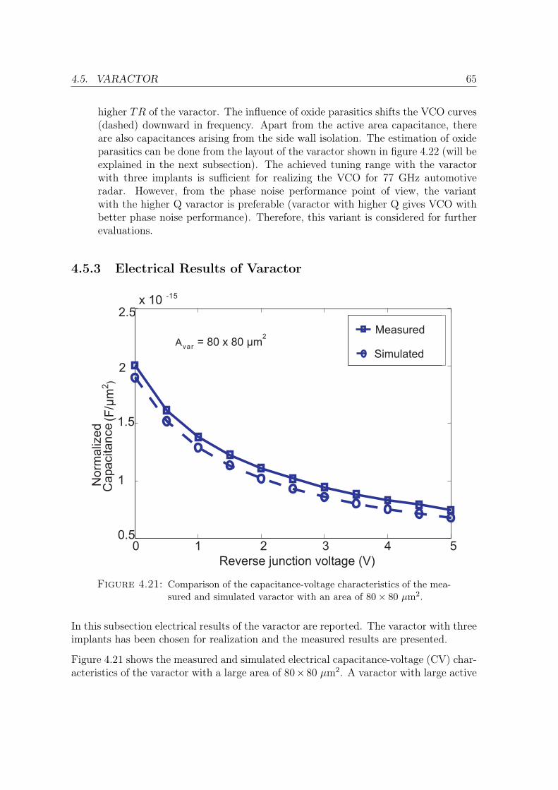
4.5. VARACTOR 65
higher TR of the varactor. The influence of oxide parasitics shifts the VCO curves(dashed) downward in frequency. Apart from the active area capacitance, thereare also capacitances arising from the side wall isolation. The estimation of oxideparasitics can be done from the layout of the varactor shown in figure 4.22 (will beexplained in the next subsection). The achieved tuning range with the varactorwith three implants is sufficient for realizing the VCO for 77 GHz automotiveradar. However, from the phase noise performance point of view, the variantwith the higher Q varactor is preferable (varactor with higher Q gives VCO withbetter phase noise performance). Therefore, this variant is considered for furtherevaluations.
4.5.3 Electrical Results of Varactor
Reverse junction voltage (V)
No
rma
lize
dC
apa
cita
nce
(F/μ
m)
2
A = 80 x 80 μmvar
2Measured
Simulated
x 10 -15
0 1 2 3 4 5
2.5
2
1.5
1
0.5
Figure 4.21: Comparison of the capacitance-voltage characteristics of the mea-sured and simulated varactor with an area of 80× 80 μm2.
In this subsection electrical results of the varactor are reported. The varactor with threeimplants has been chosen for realization and the measured results are presented.
Figure 4.21 shows the measured and simulated electrical capacitance-voltage (CV) char-acteristics of the varactor with a large area of 80×80 μm2. A varactor with large active
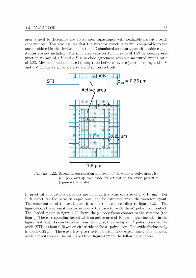
4.5. VARACTOR 66
area is used to determine the active area capacitance with negligible parasitic oxidecapacitances. This also assures that the varactor structure is well comparable to theone considered in the simulation. In the 1-D simulated structure, parasitic oxide capac-itances are not included. The simulated varactor tuning ratio of 1.89 between reversejunction voltage of 1 V and 5 V is in close agreement with the measured tuning ratioof 1.88. Measured and simulated tuning ratio between reverse junction voltages of 0 Vand 5 V for the varactor are 2.77 and 2.75, respectively.
Active area
STI
1 μm
1.5 μm
= 0.25 μm
0.25 μm
p-poly
p-poly
10 μm
dox
Active area
STI
1 μm
1.5 μm
= 0.25 μm
0.25 μm
p-poly
p-poly
10 μm
dox
Figure 4.22: Schematic cross section and layout of the varactor active area withp+- poly overlap over oxide for estimating the oxide parasitics(figure not to scale).
In practical applications varactors are built with a basic cell size of 1 × 10 μm2. Forsuch structures the parasitic capacitance can be estimated from the varactor layout.The contribution of the oxide parasitics is estimated according to figure 4.22. Thefigure shows the schematic cross section of the varactor with the p+ polysilicon contact.The shaded region in figure 4.22 shows the p+ polysilicon contact to the varactor (topfigure). The corresponding layout with an active area of 10 μm2 is also included in thefigure (bottom). As can be noted from the figure, the overlap of p+ polysilicon over theoxide (STI) is about 0.25 μm on either side of the p+ polysilicon. The oxide thickness dox
is about 0.25 μm. These overlaps give rise to parasitic oxide capacitance. The parasiticoxide capacitance can be estimated from figure 4.22 by the following equation
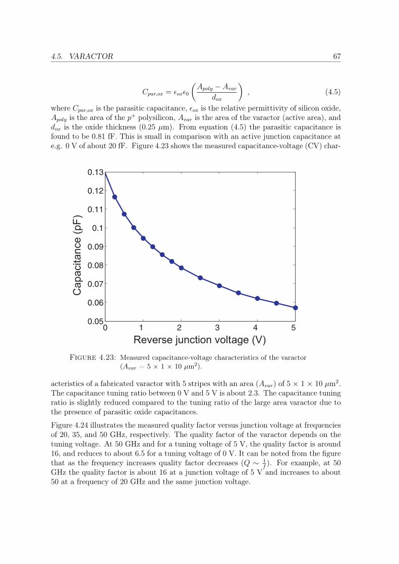
4.5. VARACTOR 67
Cpar,ox = εoxε0
(Apoly − Avar
dox
), (4.5)
where Cpar,ox is the parasitic capacitance, εox is the relative permittivity of silicon oxide,Apoly is the area of the p+ polysilicon, Avar is the area of the varactor (active area), anddox is the oxide thickness (0.25 μm). From equation (4.5) the parasitic capacitance isfound to be 0.81 fF. This is small in comparison with an active junction capacitance ate.g. 0 V of about 20 fF. Figure 4.23 shows the measured capacitance-voltage (CV) char-
Reverse junction voltage (V)
Capacitance
(pF
)
Figure 4.23: Measured capacitance-voltage characteristics of the varactor(Avar = 5 × 1 × 10 μm2).
acteristics of a fabricated varactor with 5 stripes with an area (Avar) of 5 × 1 × 10 μm2.The capacitance tuning ratio between 0 V and 5 V is about 2.3. The capacitance tuningratio is slightly reduced compared to the tuning ratio of the large area varactor due tothe presence of parasitic oxide capacitances.
Figure 4.24 illustrates the measured quality factor versus junction voltage at frequenciesof 20, 35, and 50 GHz, respectively. The quality factor of the varactor depends on thetuning voltage. At 50 GHz and for a tuning voltage of 5 V, the quality factor is around16, and reduces to about 6.5 for a tuning voltage of 0 V. It can be noted from the figurethat as the frequency increases quality factor decreases (Q ∼ 1
f). For example, at 50
GHz the quality factor is about 16 at a junction voltage of 5 V and increases to about50 at a frequency of 20 GHz and the same junction voltage.
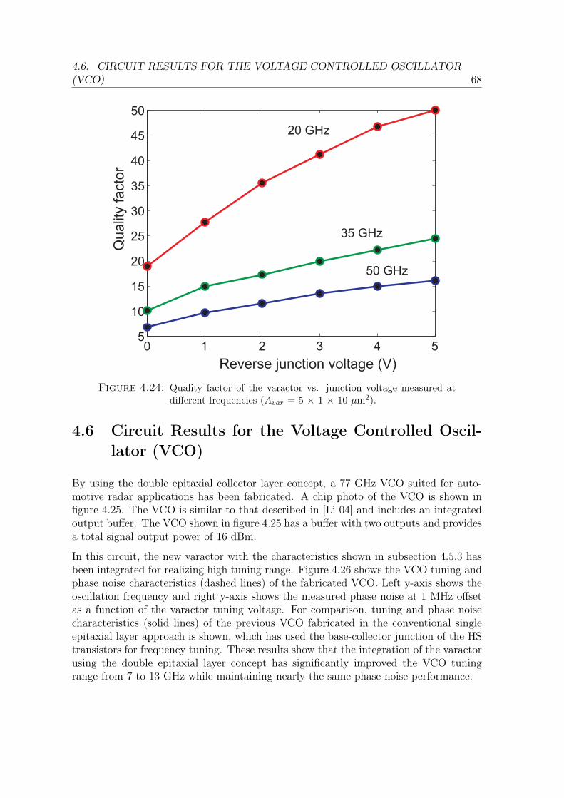
4.6. CIRCUIT RESULTS FOR THE VOLTAGE CONTROLLED OSCILLATOR(VCO) 68
5432105
10
15
20
25
30
35
40
45
50
Reverse junction voltage (V)
Qualit
yfa
cto
r
35 GHz
50 GHz
20 GHz
Figure 4.24: Quality factor of the varactor vs. junction voltage measured atdifferent frequencies (Avar = 5 × 1 × 10 μm2).
4.6 Circuit Results for the Voltage Controlled Oscil-
lator (VCO)
By using the double epitaxial collector layer concept, a 77 GHz VCO suited for auto-motive radar applications has been fabricated. A chip photo of the VCO is shown infigure 4.25. The VCO is similar to that described in [Li 04] and includes an integratedoutput buffer. The VCO shown in figure 4.25 has a buffer with two outputs and providesa total signal output power of 16 dBm.
In this circuit, the new varactor with the characteristics shown in subsection 4.5.3 hasbeen integrated for realizing high tuning range. Figure 4.26 shows the VCO tuning andphase noise characteristics (dashed lines) of the fabricated VCO. Left y-axis shows theoscillation frequency and right y-axis shows the measured phase noise at 1 MHz offsetas a function of the varactor tuning voltage. For comparison, tuning and phase noisecharacteristics (solid lines) of the previous VCO fabricated in the conventional singleepitaxial layer approach is shown, which has used the base-collector junction of the HStransistors for frequency tuning. These results show that the integration of the varactorusing the double epitaxial layer concept has significantly improved the VCO tuningrange from 7 to 13 GHz while maintaining nearly the same phase noise performance.
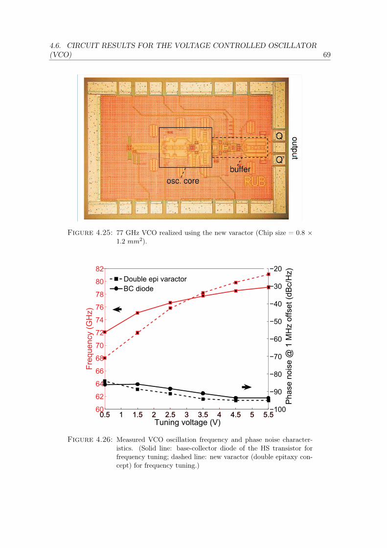
4.6. CIRCUIT RESULTS FOR THE VOLTAGE CONTROLLED OSCILLATOR(VCO) 69
Figure 4.25: 77 GHz VCO realized using the new varactor (Chip size = 0.8 ×1.2 mm2).
0.5 1 1.5 2 2.5 3 3.5 4 4.5 5 5.560
62
64
66
68
70
72
74
76
78
80
82
Freq
uenc
y (G
Hz)
0.5 1 1.5 2 2.5 3 3.5 4 4.5 5 5.5−100
−90
−80
−70
−60
−50
−40
−30
−20
Tuning voltage (V)
Pha
se n
oise
@ 1
MH
z of
fset
(dB
c/H
z)Double epi varactorBC diode
Figure 4.26: Measured VCO oscillation frequency and phase noise character-istics. (Solid line: base-collector diode of the HS transistor forfrequency tuning; dashed line: new varactor (double epitaxy con-cept) for frequency tuning.)
Chapter 5
Optimization of SiGe HBT for Higher
Performance
In this chapter, various optimizations of the high speed (HS) transistor for improvingthe performance in terms of transit frequency fT and maximum oscillation frequencyfmax are investigated by means of 1-D and 2-D device simulations. These optimizationsinclude investigation of individual regions (emitter, base, and collector) of the HS tran-sistor for achieving the higher performance. As a part of emitter optimization, the effectof emitter silicon cap doping and thickness on the frequency performance is investigated.This is followed by a description of determining the optimum thickness and doping ofthe collector for obtaining higher performance. Finally, as a part of base optimization,various ways to reduce the total base resistance Rb,tot for improving the performance ofthe HS transistor are investigated and the results are presented.
5.1 Introduction
The frequency performance of the HS transistor can be improved by optimizing thevertical profiles and lateral profiles, and by reducing parasitics. The two most importantfigures-of-merit (FOM) that are considered in the simulation study are fT and fmax.fT and fmax are widely used as figures-of-merit to characterize high-frequency bipolartechnologies.
fT can be improved by reducing the delay components, which are related to fT in thewell-established relationship shown below,
1
2πfT
= τec = τe + τb + τeb +wBC
2υsat︸ ︷︷ ︸τf
+kT
qIC
(CBE + CBC) + CBC(Re + Rc) , (5.1)
70
5.2. EMITTER OPTIMIZATION 71
where τec is the emitter-collector transit time, τf is the forward transit time1, τe is theemitter transit time, τb is the base transit time, τeb is the emitter-base space charge layertransit time, wBC is the base-collector space charge layer width, and υsat is the electronsaturation velocity. These time constants have been discussed in detail in section 2.4.1.CBE and CBC are the base-emitter and base-collector capacitances, respectively. Re andRc are the emitter and collector resistances, respectively. IC is the collector current, kis Boltzmann’s constant, T is the temperature, and q is the elementary charge.
fT mainly depends on the vertical doping profiles. At optimum current, fT is deter-mined by τf . It depends weakly on capacitances (CBE and CBC) at sufficiently highcurrents. The main components of τf are τb and τbc = wBC
2υsat. In order to increase fT ,
τf and the capacitance terms have to be reduced. In modern SiGe HBTs, τb is signif-icantly reduced due to a very shallow base, and additionally due to Ge profile gradingin the base [Harame 95]. τbc can be reduced by increasing the collector doping and byfurther reducing the collector dimension. Thus, the transit time components τb and τbc
are reduced through the reduction of vertical dimension and Ge profile optimization.Capacitance terms can be reduced by optimizing the doping profiles in the space chargelayers.
Though fT is one of the important FOMs and gives information about the quality ofthe vertical doping profile of the transistor, it does not include the effect of parasiticslike the base resistance Rb,tot and not sufficiently of the base-collector capacitance CBC ,which are important in determining the frequency behavior of the transistor in practicalcircuit configurations. Consequently, other FOMs have been proposed and discussed inthe literature [Taur 98]. One that is relatively simple and easy to use is fmax, which isthe frequency at which the unilateral power gain becomes unity. It takes into accountkey parasitic elements and better predicts digital switching delay, and is related to fT
through the following relation [Pritchard 55,Roulston 90],
fmax =
√fT
8πRb,totCBC
. (5.2)
It can be seen that equation (5.2) includes the effect of fT , Rb,tot, and CBC equally, andhence is a more realistic performance indicator.
5.2 Emitter Optimization
This section describes different investigations of the emitter silicon cap (including a p-doped silicon cap, an n-doped silicon cap, and an un-doped silicon cap) by means of1-D device simulations. Device simulations are used to find the optimum silicon cap
1The forward transit time models the excess minority charge stored in the transistor when itsemitter-base junction is forward biased and its base-collector junction is reverse biased.
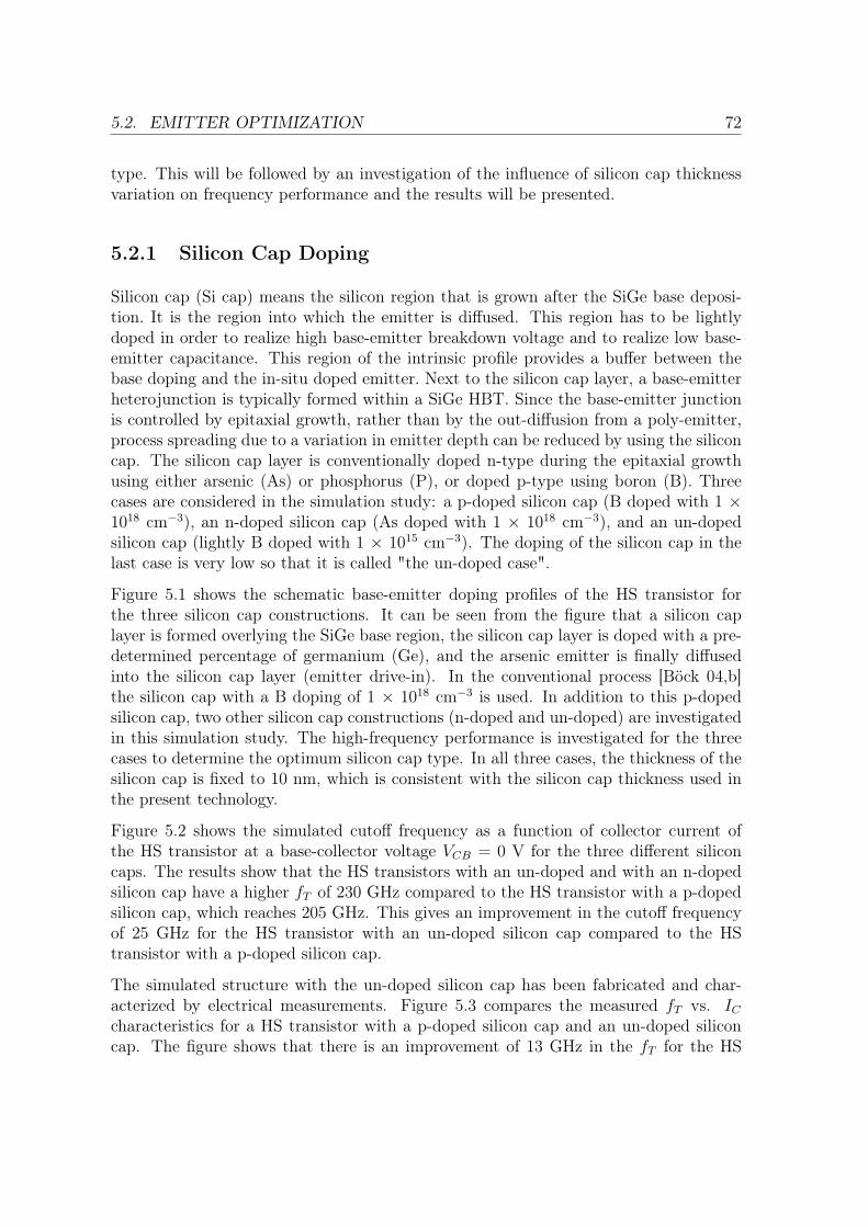
5.2. EMITTER OPTIMIZATION 72
type. This will be followed by an investigation of the influence of silicon cap thicknessvariation on frequency performance and the results will be presented.
5.2.1 Silicon Cap Doping
Silicon cap (Si cap) means the silicon region that is grown after the SiGe base deposi-tion. It is the region into which the emitter is diffused. This region has to be lightlydoped in order to realize high base-emitter breakdown voltage and to realize low base-emitter capacitance. This region of the intrinsic profile provides a buffer between thebase doping and the in-situ doped emitter. Next to the silicon cap layer, a base-emitterheterojunction is typically formed within a SiGe HBT. Since the base-emitter junctionis controlled by epitaxial growth, rather than by the out-diffusion from a poly-emitter,process spreading due to a variation in emitter depth can be reduced by using the siliconcap. The silicon cap layer is conventionally doped n-type during the epitaxial growthusing either arsenic (As) or phosphorus (P), or doped p-type using boron (B). Threecases are considered in the simulation study: a p-doped silicon cap (B doped with 1 ×1018 cm−3), an n-doped silicon cap (As doped with 1 × 1018 cm−3), and an un-dopedsilicon cap (lightly B doped with 1 × 1015 cm−3). The doping of the silicon cap in thelast case is very low so that it is called "the un-doped case".
Figure 5.1 shows the schematic base-emitter doping profiles of the HS transistor forthe three silicon cap constructions. It can be seen from the figure that a silicon caplayer is formed overlying the SiGe base region, the silicon cap layer is doped with a pre-determined percentage of germanium (Ge), and the arsenic emitter is finally diffusedinto the silicon cap layer (emitter drive-in). In the conventional process [Böck 04,b]the silicon cap with a B doping of 1 × 1018 cm−3 is used. In addition to this p-dopedsilicon cap, two other silicon cap constructions (n-doped and un-doped) are investigatedin this simulation study. The high-frequency performance is investigated for the threecases to determine the optimum silicon cap type. In all three cases, the thickness of thesilicon cap is fixed to 10 nm, which is consistent with the silicon cap thickness used inthe present technology.
Figure 5.2 shows the simulated cutoff frequency as a function of collector current ofthe HS transistor at a base-collector voltage VCB = 0 V for the three different siliconcaps. The results show that the HS transistors with an un-doped and with an n-dopedsilicon cap have a higher fT of 230 GHz compared to the HS transistor with a p-dopedsilicon cap, which reaches 205 GHz. This gives an improvement in the cutoff frequencyof 25 GHz for the HS transistor with an un-doped silicon cap compared to the HStransistor with a p-doped silicon cap.
The simulated structure with the un-doped silicon cap has been fabricated and char-acterized by electrical measurements. Figure 5.3 compares the measured fT vs. IC
characteristics for a HS transistor with a p-doped silicon cap and an un-doped siliconcap. The figure shows that there is an improvement of 13 GHz in the fT for the HS
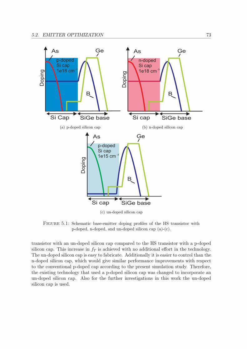
5.2. EMITTER OPTIMIZATION 73
Ge
B
As
p-dopedSi cap1e18 cm
-3
SiGe baseSi Cap
Do
pin
g
(a) p-doped silicon cap
Ge
B
As
n-dopedSi cap1e18 cm
-3
SiGe baseSi capD
op
ing
(b) n-doped silicon cap
Ge
B
As
p-dopedSi cap1e15 cm -3
SiGe baseSi cap
Dopin
g
(c) un-doped silicon cap
Figure 5.1: Schematic base-emitter doping profiles of the HS transistor withp-doped, n-doped, and un-doped silicon cap (a)-(c).
transistor with an un-doped silicon cap compared to the HS transistor with a p-dopedsilicon cap. This increase in fT is achieved with no additional effort in the technology.The un-doped silicon cap is easy to fabricate. Additionally it is easier to control than then-doped silicon cap, which would give similar performance improvements with respectto the conventional p-doped cap according to the present simulation study. Therefore,the existing technology that used a p-doped silicon cap was changed to incorporate anun-doped silicon cap. Also for the further investigations in this work the un-dopedsilicon cap is used.
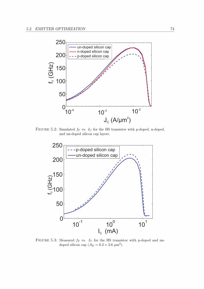
5.2. EMITTER OPTIMIZATION 74
un-doped silicon cap
n-doped silicon cap
p-doped silicon cap
250
200
150
100
0
50
10-4
10-3 10
-2
J (A/μm )C
2
f(G
Hz)
T
Figure 5.2: Simulated fT vs. IC for the HS transistor with p-doped, n-doped,and un-doped silicon cap layers.
10-1
100
101
0
50
100
150
200
250p-doped silicon cap
un-doped silicon cap
IC (mA)
f(G
Hz)
T
Figure 5.3: Measured fT vs. IC for the HS transistor with p-doped and un-doped silicon cap (AE = 0.2× 2.6 μm2).
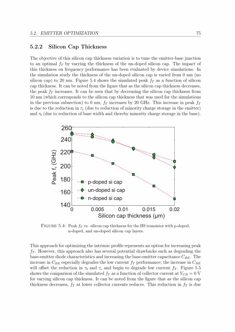
5.2. EMITTER OPTIMIZATION 75
5.2.2 Silicon Cap Thickness
The objective of this silicon cap thickness variation is to tune the emitter-base junctionto an optimal fT by varying the thickness of the un-doped silicon cap. The impact ofthis thickness on frequency performance has been evaluated by device simulations. Inthe simulation study the thickness of the un-doped silicon cap is varied from 0 nm (nosilicon cap) to 20 nm. Figure 5.4 shows the simulated peak fT as a function of siliconcap thickness. It can be noted from the figure that as the silicon cap thickness decreases,the peak fT increases. It can be seen that by decreasing the silicon cap thickness from10 nm (which corresponds to the silicon cap thickness that was used for the simulationsin the previous subsection) to 0 nm, fT increases by 20 GHz. This increase in peak fT
is due to the reduction in τe (due to reduction of minority charge storage in the emitter)and τb (due to reduction of base width and thereby minority charge storage in the base).
Silicon cap thickness (μm)
Peak
f(G
Hz)
T
260
240
220
200
180
160
140
Figure 5.4: Peak fT vs. silicon cap thickness for the HS transistor with p-doped,n-doped, and un-doped silicon cap layers.
This approach for optimizing the intrinsic profile represents an option for increasing peakfT . However, this approach also has several potential drawbacks such as degrading thebase-emitter diode characteristics and increasing the base-emitter capacitance CBE. Theincrease in CBE especially degrades the low current fT performance; the increase in CBE
will offset the reduction in τb and τe and begin to degrade low current fT . Figure 5.5shows the comparison of the simulated fT as a function of collector current at VCB = 0 Vfor varying silicon cap thickness. It can be noted from the figure that as the silicon capthickness decreases, fT at lower collector currents reduces. This reduction in fT is due
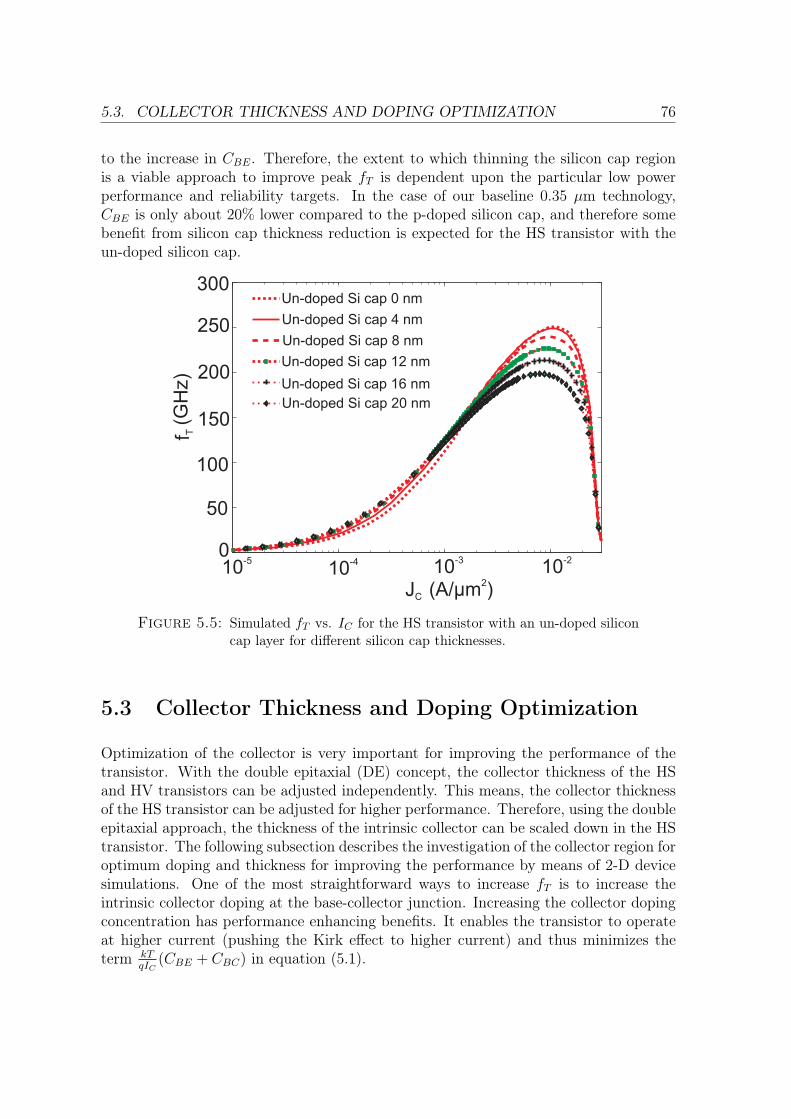
5.3. COLLECTOR THICKNESS AND DOPING OPTIMIZATION 76
to the increase in CBE. Therefore, the extent to which thinning the silicon cap regionis a viable approach to improve peak fT is dependent upon the particular low powerperformance and reliability targets. In the case of our baseline 0.35 μm technology,CBE is only about 20% lower compared to the p-doped silicon cap, and therefore somebenefit from silicon cap thickness reduction is expected for the HS transistor with theun-doped silicon cap.
JC (A/μm )2
f(G
Hz)
T
Un-doped Si cap 0 nm
Un-doped Si cap 4 nm
Un-doped Si cap 8 nm
Un-doped Si cap 12 nm
Un-doped Si cap 16 nm
Un-doped Si cap 20 nm
300
250
200
150
100
50
10-5
10-4 10
-310
-20
Figure 5.5: Simulated fT vs. IC for the HS transistor with an un-doped siliconcap layer for different silicon cap thicknesses.
5.3 Collector Thickness and Doping Optimization
Optimization of the collector is very important for improving the performance of thetransistor. With the double epitaxial (DE) concept, the collector thickness of the HSand HV transistors can be adjusted independently. This means, the collector thicknessof the HS transistor can be adjusted for higher performance. Therefore, using the doubleepitaxial approach, the thickness of the intrinsic collector can be scaled down in the HStransistor. The following subsection describes the investigation of the collector region foroptimum doping and thickness for improving the performance by means of 2-D devicesimulations. One of the most straightforward ways to increase fT is to increase theintrinsic collector doping at the base-collector junction. Increasing the collector dopingconcentration has performance enhancing benefits. It enables the transistor to operateat higher current (pushing the Kirk effect to higher current) and thus minimizes theterm kT
qIC(CBE + CBC) in equation (5.1).
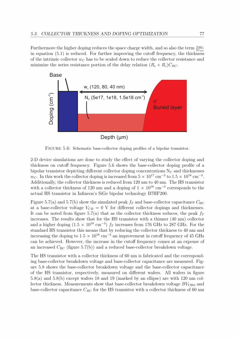
5.3. COLLECTOR THICKNESS AND DOPING OPTIMIZATION 77
Furthermore the higher doping reduces the space charge width, and so also the term wBC
2υsat
in equation (5.1) is reduced. For further improving the cutoff frequency, the thicknessof the intrinsic collector wC has to be scaled down to reduce the collector resistance andminimize the series resistance portion of the delay relation (Re + Rc)CBC .
Dopin
g(c
m)
-3
Depth (μm)
Base
w (120, 80, 40 nm)c
N (5e17, 1e18, 1.5e18 cm )C
-3
nBuried layer
+
Figure 5.6: Schematic base-collector doping profiles of a bipolar transistor.
2-D device simulations are done to study the effect of varying the collector doping andthickness on cutoff frequency. Figure 5.6 shows the base-collector doping profile of abipolar transistor depicting different collector doping concentrations NC and thicknesseswC . In this work the collector doping is increased from 5 × 1017 cm−3 to 1.5 × 1018 cm−3.Additionally, the collector thickness is reduced from 120 nm to 40 nm. The HS transistorwith a collector thickness of 120 nm and a doping of 1 × 1018 cm−3 corresponds to theactual HS transistor in Infineon’s SiGe bipolar technology B7HF200.
Figure 5.7(a) and 5.7(b) show the simulated peak fT and base-collector capacitance CBC
at a base-collector voltage VCB = 0 V for different collector dopings and thicknesses.It can be noted from figure 5.7(a) that as the collector thickness reduces, the peak fT
increases. The results show that for the HS transistor with a thinner (40 nm) collectorand a higher doping (1.5 × 1018 cm−3) fT increases from 176 GHz to 287 GHz. For thestandard HS transistor this means that by reducing the collector thickness to 40 nm andincreasing the doping to 1.5 × 1018 cm−3 an improvement in cutoff frequency of 45 GHzcan be achieved. However, the increase in the cutoff frequency comes at an expense ofan increased CBC (figure 5.7(b)) and a reduced base-collector breakdown voltage.
The HS transistor with a collector thickness of 60 nm is fabricated and the correspond-ing base-collector breakdown voltage and base-collector capacitance are measured. Fig-ure 5.8 shows the base-collector breakdown voltage and the base-collector capacitanceof the HS transistor, respectively, measured on different wafers. All wafers in figure5.8(a) and 5.8(b) except wafers 18 and 19 (marked by an ellipse) are with 120 nm col-lector thickness. Measurements show that base-collector breakdown voltage BVCBO andbase-collector capacitance CBC for the HS transistor with a collector thickness of 60 nm
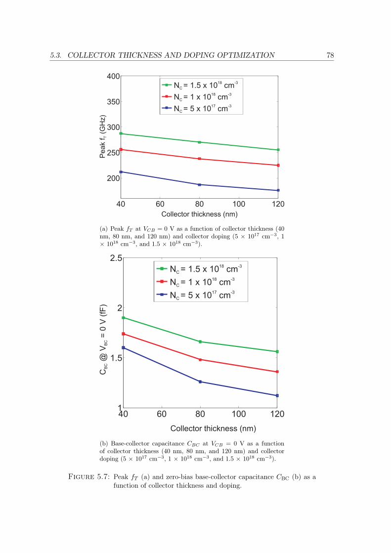
5.3. COLLECTOR THICKNESS AND DOPING OPTIMIZATION 78
40 60 80 100 120
200
250
300
350
400N = 1.5 x 10 cmC
18 -3
N = 1 x 10 cmC
18 -3
N = 5 x 10 cmC
17 -3
Collector thickness (nm)
Pe
ak
f(G
Hz)
T
(a) Peak fT at VCB = 0 V as a function of collector thickness (40nm, 80 nm, and 120 nm) and collector doping (5 × 1017 cm−3, 1× 1018 cm−3, and 1.5 × 1018 cm−3).
40 60 80 100 1201
1.5
2
2.5
N = 1.5 x 10 cmC
18 -3
N = 1 x 10 cmC
18 -3
N = 5 x 10 cmC
17 -3
Collector thickness (nm)
C@
V=
0V
(fF
)B
CB
C
(b) Base-collector capacitance CBC at VCB = 0 V as a functionof collector thickness (40 nm, 80 nm, and 120 nm) and collectordoping (5 × 1017 cm−3, 1 × 1018 cm−3, and 1.5 × 1018 cm−3).
Figure 5.7: Peak fT (a) and zero-bias base-collector capacitance CBC (b) as afunction of collector thickness and doping.
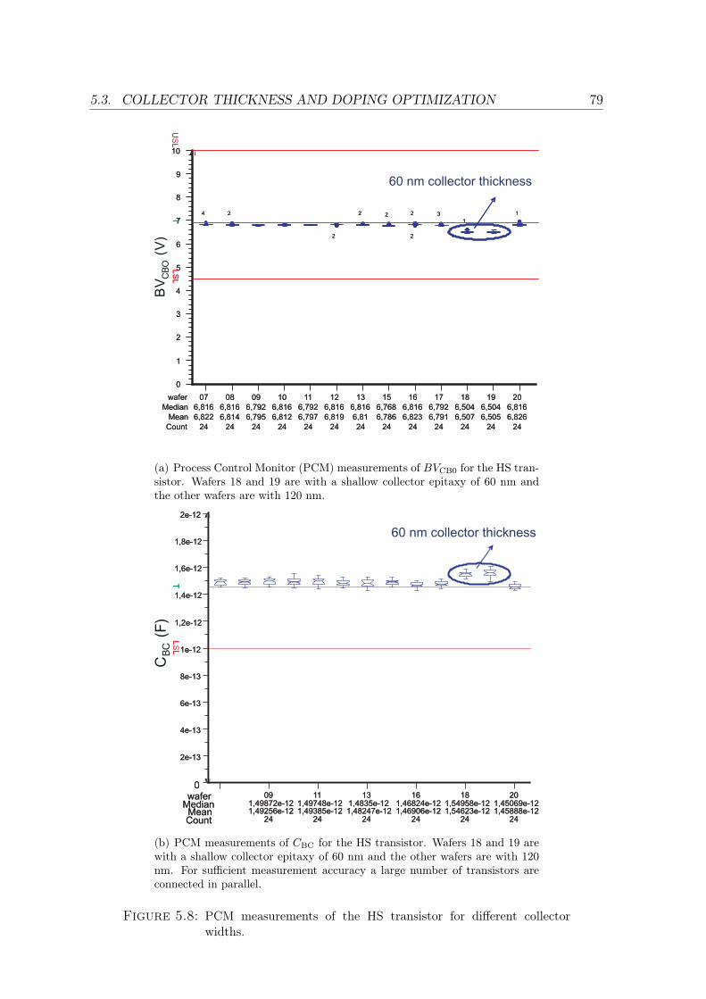
5.3. COLLECTOR THICKNESS AND DOPING OPTIMIZATION 79
07
6,816
6,822
24
08
6,816
6,814
24
09
6,792
6,795
24
10
6,816
6,812
24
11
6,792
6,797
24
12
6,816
6,819
24
13
6,816
6,81
24
15
6,768
6,786
24
16
6,816
6,823
24
17
6,792
6,791
24
18
6,504
6,507
24
19
6,504
6,505
24
20
6,816
6,826
24
wafer
Median
Mean
Count
0
1
2
3
4
5
6
7
8
9
10
4 2 2 2 2 3
1
1
2 2
LS
LU
SL
T
07
6,816
6,822
24
08
6,816
6,814
24
09
6,792
6,795
24
10
6,816
6,812
24
11
6,792
6,797
24
12
6,816
6,819
24
13
6,816
6,81
24
15
6,768
6,786
24
16
6,816
6,823
24
17
6,792
6,791
24
18
6,504
6,507
24
19
6,504
6,505
24
20
6,816
6,826
24
wafer
Median
Mean
Count
0
1
2
3
4
5
6
7
8
9
10
4 2 2 2 2 3
1
1
2 2
LS
LU
LT
60 nm collector thickness
BV
CB
O(V
)
(a) Process Control Monitor (PCM) measurements of BVCB0 for the HS tran-sistor. Wafers 18 and 19 are with a shallow collector epitaxy of 60 nm andthe other wafers are with 120 nm.
091,49872e-121,49256e-12
24
111,49748e-121,49385e-12
24
131,4835e-121,48247e-12
24
161,46824e-121,46906e-12
24
181,54958e-121,54623e-12
24
201,45069e-121,45888e-12
24
waferMedianMeanCount
0
2e-13
4e-13
6e-13
8e-13
1e-12
1,2e-12
1,4e-12
1,6e-12
1,8e-12
2e-12
LS
LT
091,49872e-121,49256e-12
24
111,49748e-121,49385e-12
24
131,4835e-121,48247e-12
24
161,46824e-121,46906e-12
24
181,54958e-121,54623e-12
24
201,45069e-121,45888e-12
24
waferMedianMeanCount
0
2e-13
4e-13
6e-13
8e-13
1e-12
1,2e-12
1,4e-12
1,6e-12
1,8e-12
2e-12
LL
T60 nm collector thickness
CB
C(F
)
(b) PCM measurements of CBC for the HS transistor. Wafers 18 and 19 arewith a shallow collector epitaxy of 60 nm and the other wafers are with 120nm. For sufficient measurement accuracy a large number of transistors areconnected in parallel.
Figure 5.8: PCM measurements of the HS transistor for different collectorwidths.
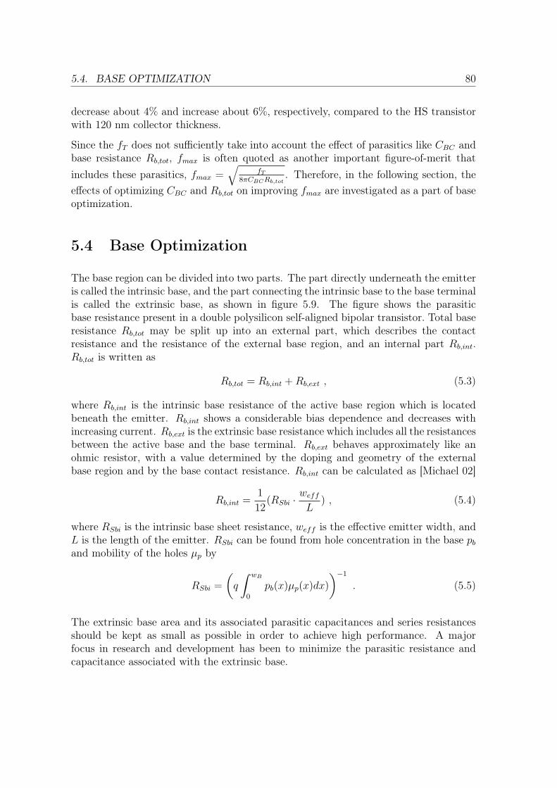
5.4. BASE OPTIMIZATION 80
decrease about 4% and increase about 6%, respectively, compared to the HS transistorwith 120 nm collector thickness.
Since the fT does not sufficiently take into account the effect of parasitics like CBC andbase resistance Rb,tot, fmax is often quoted as another important figure-of-merit that
includes these parasitics, fmax =√
fT
8πCBCRb,tot. Therefore, in the following section, the
effects of optimizing CBC and Rb,tot on improving fmax are investigated as a part of baseoptimization.
5.4 Base Optimization
The base region can be divided into two parts. The part directly underneath the emitteris called the intrinsic base, and the part connecting the intrinsic base to the base terminalis called the extrinsic base, as shown in figure 5.9. The figure shows the parasiticbase resistance present in a double polysilicon self-aligned bipolar transistor. Total baseresistance Rb,tot may be split up into an external part, which describes the contactresistance and the resistance of the external base region, and an internal part Rb,int.Rb,tot is written as
Rb,tot = Rb,int + Rb,ext , (5.3)
where Rb,int is the intrinsic base resistance of the active base region which is locatedbeneath the emitter. Rb,int shows a considerable bias dependence and decreases withincreasing current. Rb,ext is the extrinsic base resistance which includes all the resistancesbetween the active base and the base terminal. Rb,ext behaves approximately like anohmic resistor, with a value determined by the doping and geometry of the externalbase region and by the base contact resistance. Rb,int can be calculated as [Michael 02]
Rb,int =1
12(RSbi · weff
L) , (5.4)
where RSbi is the intrinsic base sheet resistance, weff is the effective emitter width, andL is the length of the emitter. RSbi can be found from hole concentration in the base pb
and mobility of the holes μp by
RSbi =
(q
∫ wB
0
pb(x)μp(x)dx)
)−1
. (5.5)
The extrinsic base area and its associated parasitic capacitances and series resistancesshould be kept as small as possible in order to achieve high performance. A majorfocus in research and development has been to minimize the parasitic resistance andcapacitance associated with the extrinsic base.
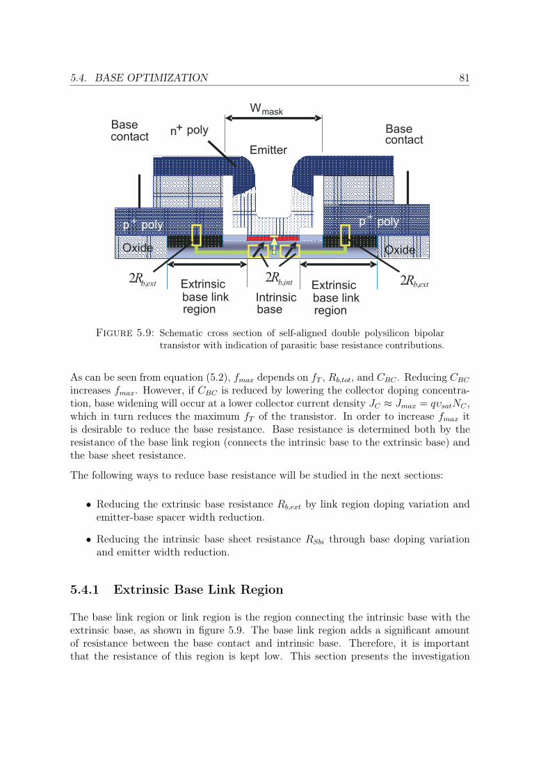
5.4. BASE OPTIMIZATION 81
Intrinsicbase
Extrinsicbase linkregion
Extrinsicbase linkregion
p+polyp+ poly
n+ poly
Oxide Oxide
Basecontact
Emitter
Basecontact
Wmask
extbR ,2 R22R
intb, extb,
Figure 5.9: Schematic cross section of self-aligned double polysilicon bipolartransistor with indication of parasitic base resistance contributions.
As can be seen from equation (5.2), fmax depends on fT , Rb,tot, and CBC . Reducing CBC
increases fmax. However, if CBC is reduced by lowering the collector doping concentra-tion, base widening will occur at a lower collector current density JC ≈ Jmax = qυsatNC ,which in turn reduces the maximum fT of the transistor. In order to increase fmax itis desirable to reduce the base resistance. Base resistance is determined both by theresistance of the base link region (connects the intrinsic base to the extrinsic base) andthe base sheet resistance.
The following ways to reduce base resistance will be studied in the next sections:
• Reducing the extrinsic base resistance Rb,ext by link region doping variation andemitter-base spacer width reduction.
• Reducing the intrinsic base sheet resistance RSbi through base doping variationand emitter width reduction.
5.4.1 Extrinsic Base Link Region
The base link region or link region is the region connecting the intrinsic base with theextrinsic base, as shown in figure 5.9. The base link region adds a significant amountof resistance between the base contact and intrinsic base. Therefore, it is importantthat the resistance of this region is kept low. This section presents the investigation
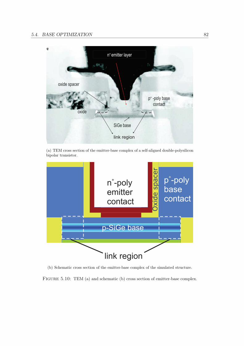
5.4. BASE OPTIMIZATION 82
Link region
SiGe base
p+ -poly base
contact
oxide spacer
n+ emitter layer
oxide
SiGe base
p+ -poly base
contact
oxide spacer
n+ emitter layer
oxide
link region
(a) TEM cross section of the emitter-base complex of a self-aligned double-polysiliconbipolar transistor.
Oxid
espacer
link region
n -polyemittercontact
+ p -polybasecontact
+
p-SiGe base
(b) Schematic cross section of the emitter-base complex of the simulated structure.
Figure 5.10: TEM (a) and schematic (b) cross section of emitter-base complex.
5.4. BASE OPTIMIZATION 83
0.25 0.3 0.3510
16
1018
1020
Depth (μm)
Dopin
g(c
m-3
)
Acceptors
5e18 cm-3
1e19 cm-3
5e19 cm-3
1e20 cm-3
2e20 cm-3
link region
Figure 5.11: Vertical doping profiles in the extrinsic base region that have beenused in the simulations.
performed for reducing the extrinsic base resistance for improving the performance interms of fmax.
A transmission electron microscope (TEM) cross section of the emitter-base complexof the HS transistor is shown in figure 5.10(a). The figure shows the heavily doped n+
emitter and extrinsic p+ polysilicon base electrodes that are separated by a thin oxidespacer. During the selective base deposition process, the intrinsic SiGe base layer, whichis growing bottom up on the collector, is connected with the polycrystalline base linkregion, which is growing top down from the base electrodes. This region is representedby dotted lines in the figure. This is called the link region. The formation of thislink region is described in section 2.5.2. For reducing the overall base resistance, it isadvantageous to have a low link region resistance to the extrinsic base. The resistanceof the link region can be reduced by increasing the doping in this region.
Figure 5.10(b) shows the cross section of the emitter-base complex of the simulatedtransistor with the link region. In the simulation, the link region is modelled as a rect-angular area with p+ doping representing out-diffused dopants from the p+ polysiliconas shown in the figure. Vertical doping profiles in the active region of the transistorshown in figure 5.10(b) are similar to the profiles that are shown in section 4.3.1 ofthis work. Figure 5.11 shows the vertical doping profiles in the extrinsic portion of thebase that have been used for the simulations. In order to provide a lower link regionresistance, doping in the link region is increased from 5 × 1018 cm−3 to 2 × 1020 cm−3.The corresponding doping profiles along a vertical cut-line through the extrinsic baseare depicted in figure 5.11.
In order to model the link region, the doping in the link region has to be known. But it
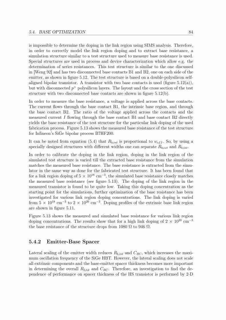
5.4. BASE OPTIMIZATION 84
is impossible to determine the doping in the link region using SIMS analysis. Therefore,in order to correctly model the link region doping and to extract base resistance, asimulation structure similar to a test structure used to measure base resistance is used.Special structures are used in process and device characterization which allow e.g. thedetermination of series resistances. This test structure is similar to the one discussedin [Weng 92] and has two disconnected base contacts B1 and B2, one on each side of theemitter, as shown in figure 5.12. The test structure is based on a double-polysilicon self-aligned bipolar transistor. A transistor with two base contacts is used (figure 5.12(a)),but with disconnected p+ polysilicon layers. The layout and the cross section of the teststructure with two disconnected base contacts are shown in figure 5.12(b).
In order to measure the base resistance, a voltage is applied across the base contacts.The current flows through the base contact B1, the intrinsic base region, and throughthe base contact B2. The ratio of the voltage applied across the contacts and themeasured current I flowing through the base contact B1 and base contact B2 directlyyields the base resistance of the test structure for the particular link doping of the usedfabrication process. Figure 5.13 shows the measured base resistance of the test structurefor Infineon’s SiGe bipolar process B7HF200.
It can be noted from equation (5.4) that Rb,int is proportional to weff . So, by using aspecially designed structures with different widths one can separate Rb,ext and Rb,int.
In order to calibrate the doping in the link region, doping in the link region of thesimulated test structure is varied till the extracted base resistance from the simulationmatches the measured base resistance. The base resistance is extracted from the simu-lator in the same way as done for the fabricated test structure. It has been found thatfor a link region doping of 5 × 1018 cm−3, the simulated base resistance closely matchesthe measured base resistance (see figure 5.13). The doping of the link region in themeasured transistor is found to be quite low. Taking this doping concentration as thestarting point for the simulations, further optimization of the base resistance has beeninvestigated for various link region doping concentrations. The link doping is variedfrom 5 × 1018 cm−3 to 2 × 1020 cm−3. Doping profiles of the extrinsic base link regionare shown in figure 5.11.
Figure 5.13 shows the measured and simulated base resistance for various link regiondoping concentrations. The results show that for a high link doping of 2 × 1020 cm−3
the base resistance of the structure drops from 1080 Ω to 946 Ω.
5.4.2 Emitter-Base Spacer
Lateral scaling of the emitter width reduces Rb,int and CBC , which increases the maxi-mum oscillation frequency of the SiGe HBT. However, the lateral scaling does not scaleall extrinsic components and the base-emitter spacer thickness becomes more importantin determining the overall Rb,tot and CBC . Therefore, an investigation to find the de-pendence of performance on spacer thickness of the HS transistor is performed by 2-D
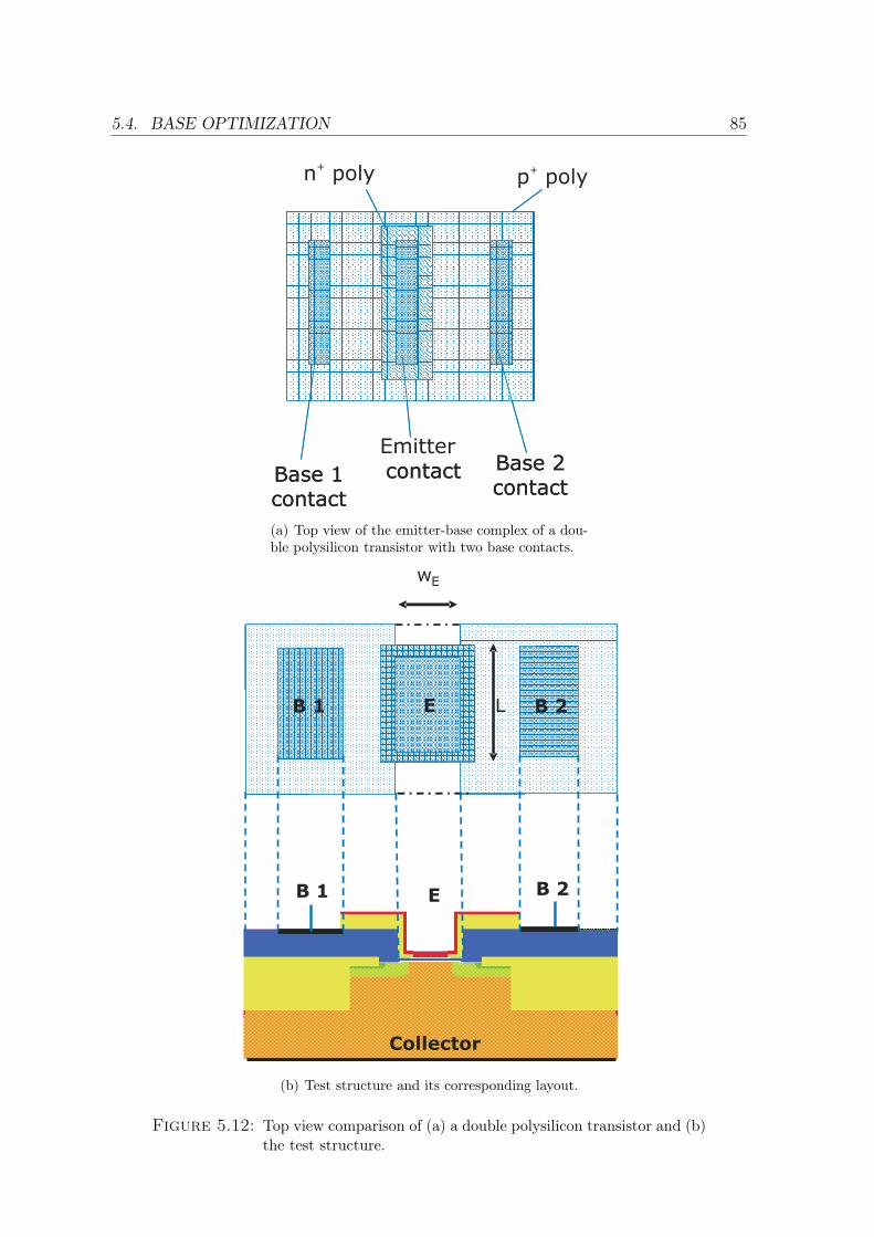
5.4. BASE OPTIMIZATION 85
p poly+
Base 1contact
Base 2contact
Emittercontact
n poly+
Base 1contact
Base 2contact
contact
(a) Top view of the emitter-base complex of a dou-ble polysilicon transistor with two base contacts.
E B 2B 1
Collector
B 2B 1 E
wE
L
(b) Test structure and its corresponding layout.
Figure 5.12: Top view comparison of (a) a double polysilicon transistor and (b)the test structure.
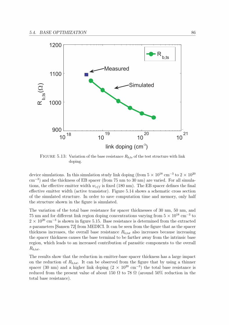
5.4. BASE OPTIMIZATION 86
1018
1019
1020
1021
900
1000
1100
1200
Rb,ts
Measured
Simulated
R(
)b,ts
�
link doping (cm )-3
Figure 5.13: Variation of the base resistance Rb,ts of the test structure with linkdoping.
device simulations. In this simulation study link doping (from 5 × 1018 cm−3 to 2 × 10²⁰
cm−3) and the thickness of EB spacer (from 75 nm to 30 nm) are varied. For all simula-tions, the effective emitter width weff is fixed (180 nm). The EB spacer defines the finaleffective emitter width (active transistor). Figure 5.14 shows a schematic cross sectionof the simulated structure. In order to save computation time and memory, only halfthe structure shown in the figure is simulated.
The variation of the total base resistance for spacer thicknesses of 30 nm, 50 nm, and75 nm and for different link region doping concentrations varying from 5 × 1018 cm−3 to2 × 1020 cm−3 is shown in figure 5.15. Base resistance is determined from the extracteds-parameters [Sansen 72] from MEDICI. It can be seen from the figure that as the spacerthickness increases, the overall base resistance Rb,tot also increases because increasingthe spacer thickness causes the base terminal to be farther away from the intrinsic baseregion, which leads to an increased contribution of parasitic components to the overallRb,tot.
The results show that the reduction in emitter-base spacer thickness has a large impacton the reduction of Rb,tot. It can be observed from the figure that by using a thinnerspacer (30 nm) and a higher link doping (2 × 1020 cm−3) the total base resistance isreduced from the present value of about 150 Ω to 78 Ω (around 50% reduction in thetotal base resistance).
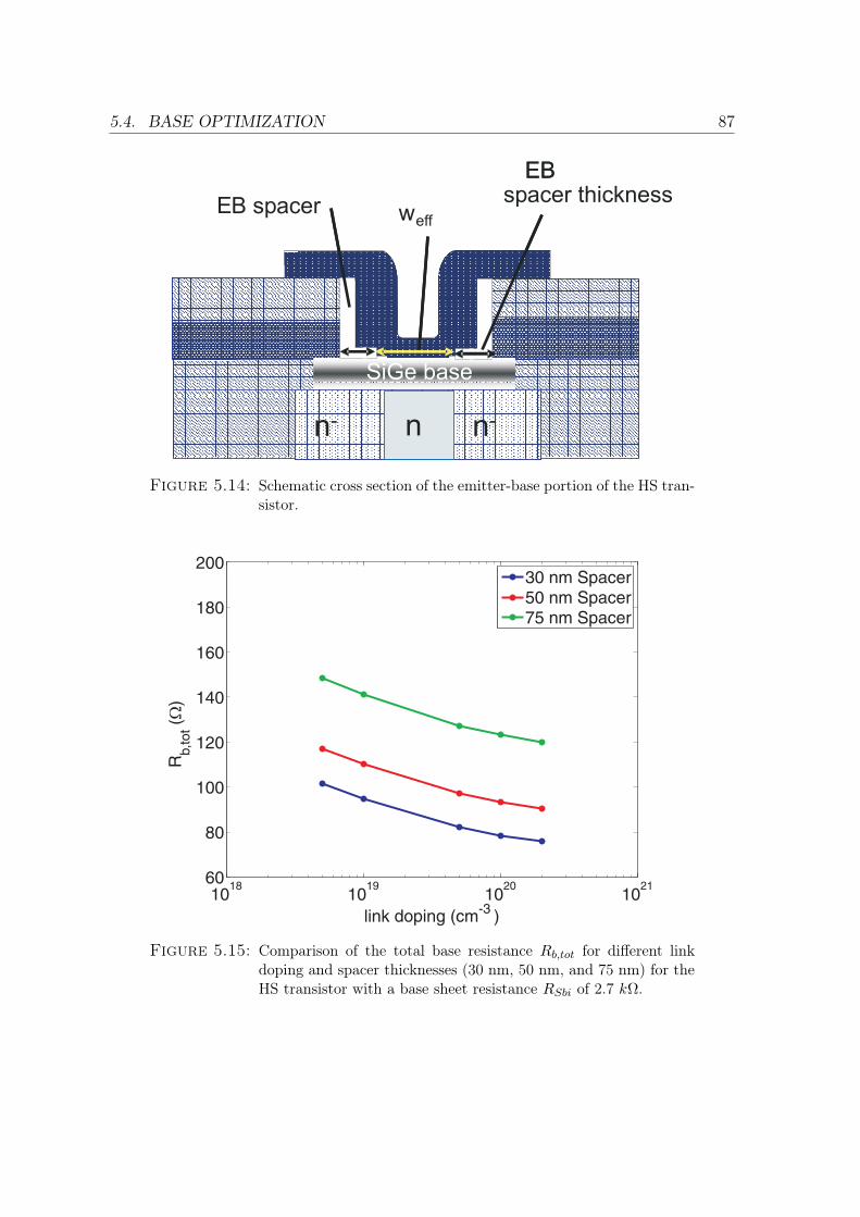
5.4. BASE OPTIMIZATION 87
n
SiGe base
B spacer
EB
nn- n-
weff
n
SiGe base
E
EBspacer thickness
nn- n-
Figure 5.14: Schematic cross section of the emitter-base portion of the HS tran-sistor.
1018
1019
1020
1021
60
80
100
120
140
160
180
200
link doping (cm-3
)
Rb,t
ot(
)�
30 nm Spacer50 nm Spacer75 nm Spacer
Figure 5.15: Comparison of the total base resistance Rb,tot for different linkdoping and spacer thicknesses (30 nm, 50 nm, and 75 nm) for theHS transistor with a base sheet resistance RSbi of 2.7 kΩ.
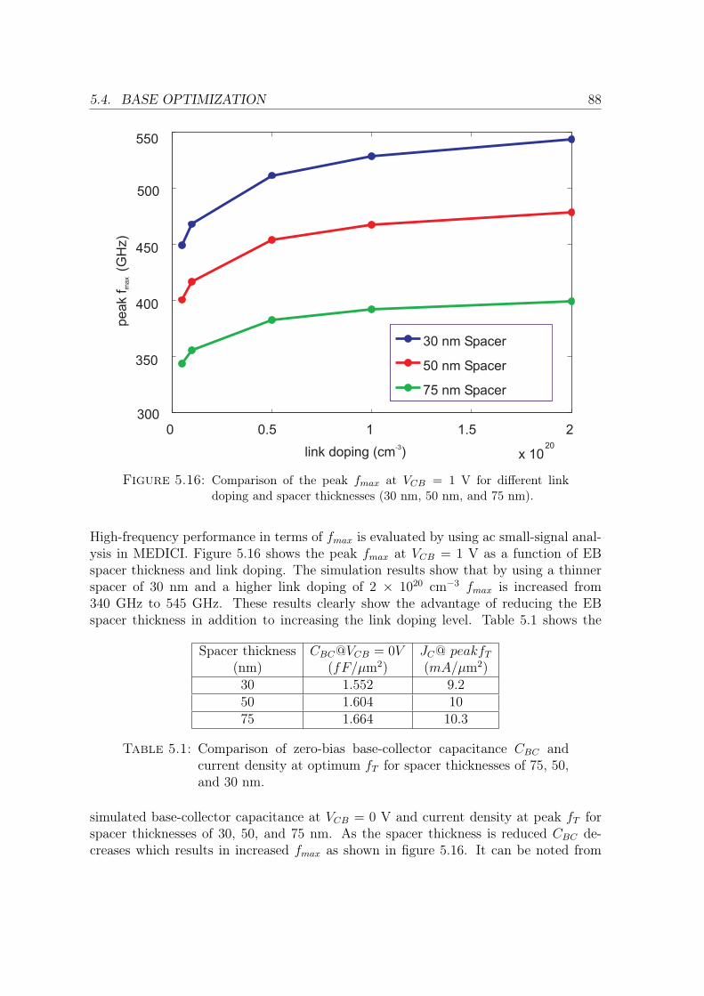
5.4. BASE OPTIMIZATION 88
0 0.5 1 1.5 2
x 1020
300
350
400
450
500
550
link doping (cm )-3
peak
f ma
x(G
Hz)
30 nm Spacer
50 nm Spacer
75 nm Spacer
Figure 5.16: Comparison of the peak fmax at VCB = 1 V for different linkdoping and spacer thicknesses (30 nm, 50 nm, and 75 nm).
High-frequency performance in terms of fmax is evaluated by using ac small-signal anal-ysis in MEDICI. Figure 5.16 shows the peak fmax at VCB = 1 V as a function of EBspacer thickness and link doping. The simulation results show that by using a thinnerspacer of 30 nm and a higher link doping of 2 × 1020 cm−3 fmax is increased from340 GHz to 545 GHz. These results clearly show the advantage of reducing the EBspacer thickness in addition to increasing the link doping level. Table 5.1 shows the
Spacer thickness CBC@VCB = 0V JC@ peakfT
(nm) (fF/μm2) (mA/μm2)30 1.552 9.250 1.604 1075 1.664 10.3
Table 5.1: Comparison of zero-bias base-collector capacitance CBC andcurrent density at optimum fT for spacer thicknesses of 75, 50,and 30 nm.
simulated base-collector capacitance at VCB = 0 V and current density at peak fT forspacer thicknesses of 30, 50, and 75 nm. As the spacer thickness is reduced CBC de-creases which results in increased fmax as shown in figure 5.16. It can be noted from
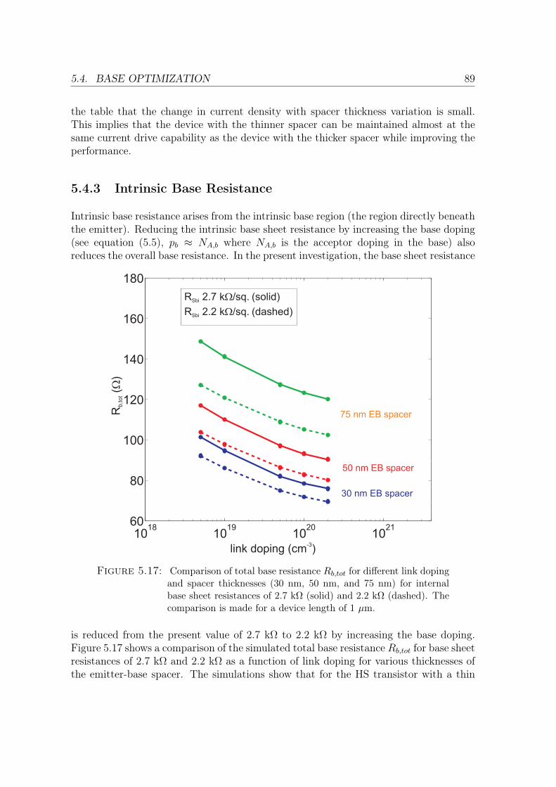
5.4. BASE OPTIMIZATION 89
the table that the change in current density with spacer thickness variation is small.This implies that the device with the thinner spacer can be maintained almost at thesame current drive capability as the device with the thicker spacer while improving theperformance.
5.4.3 Intrinsic Base Resistance
Intrinsic base resistance arises from the intrinsic base region (the region directly beneaththe emitter). Reducing the intrinsic base sheet resistance by increasing the base doping(see equation (5.5), pb ≈ NA,b where NA,b is the acceptor doping in the base) alsoreduces the overall base resistance. In the present investigation, the base sheet resistance
1018
1019
1020
1021
60
80
100
120
140
160
180
75 nm EB spacer
50 nm EB spacer
30 nm EB spacer
R 2.7 k /sq. (solid)Sbi �
R 2.2 k /sq. (dashed)Sbi �
link doping (cm )-3
R(
)b,tot
�
Figure 5.17: Comparison of total base resistance Rb,tot for different link dopingand spacer thicknesses (30 nm, 50 nm, and 75 nm) for internalbase sheet resistances of 2.7 kΩ (solid) and 2.2 kΩ (dashed). Thecomparison is made for a device length of 1 μm.
is reduced from the present value of 2.7 kΩ to 2.2 kΩ by increasing the base doping.Figure 5.17 shows a comparison of the simulated total base resistance Rb,tot for base sheetresistances of 2.7 kΩ and 2.2 kΩ as a function of link doping for various thicknesses ofthe emitter-base spacer. The simulations show that for the HS transistor with a thin
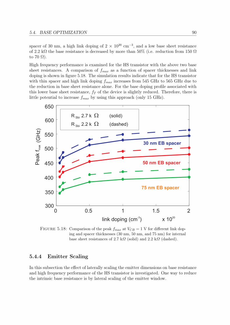
5.4. BASE OPTIMIZATION 90
spacer of 30 nm, a high link doping of 2 × 1020 cm−3, and a low base sheet resistanceof 2.2 kΩ the base resistance is decreased by more than 50% (i.e. reduction from 150 Ωto 70 Ω).
High frequency performance is examined for the HS transistor with the above two basesheet resistances. A comparison of fmax as a function of spacer thicknesses and linkdoping is shown in figure 5.18. The simulation results indicate that for the HS transistorwith thin spacer and high link doping fmax increases from 545 GHz to 565 GHz due tothe reduction in base sheet resistance alone. For the base doping profile associated withthis lower base sheet resistance, fT of the device is slightly reduced. Therefore, there islittle potential to increase fmax by using this approach (only 15 GHz).
Pe
ak
f maxx
(GH
z)
link doping (cm ) x 10-3 20
0 0.5 1 1.5 2
650
600
550
500
450
400
350
300
75 nm EB spacer
50 nm EB spacer
30 nm EB spacer
R 2.7 k (solid)Sbi �
R 2.2 k (dashed)Sbi �
Figure 5.18: Comparison of the peak fmax at VCB = 1 V for different link dop-ing and spacer thicknesses (30 nm, 50 nm, and 75 nm) for internalbase sheet resistances of 2.7 kΩ (solid) and 2.2 kΩ (dashed).
5.4.4 Emitter Scaling
In this subsection the effect of laterally scaling the emitter dimensions on base resistanceand high frequency performance of the HS transistor is investigated. One way to reducethe intrinsic base resistance is by lateral scaling of the emitter window.
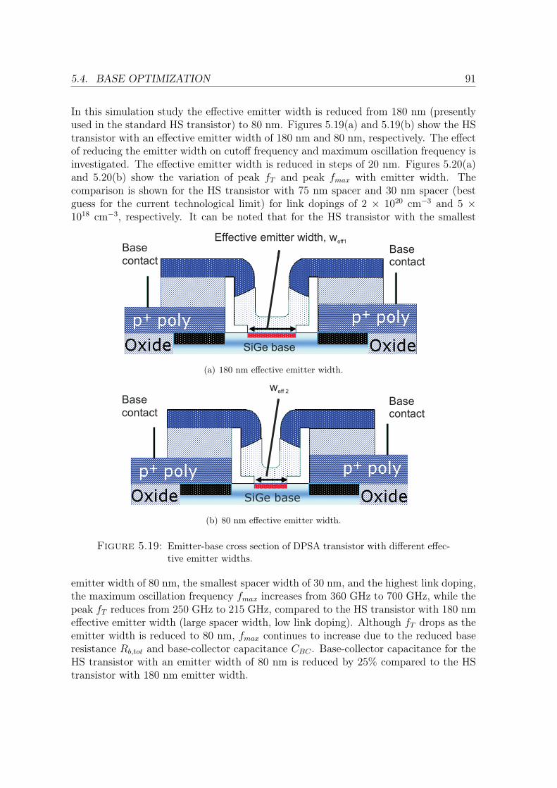
5.4. BASE OPTIMIZATION 91
In this simulation study the effective emitter width is reduced from 180 nm (presentlyused in the standard HS transistor) to 80 nm. Figures 5.19(a) and 5.19(b) show the HStransistor with an effective emitter width of 180 nm and 80 nm, respectively. The effectof reducing the emitter width on cutoff frequency and maximum oscillation frequency isinvestigated. The effective emitter width is reduced in steps of 20 nm. Figures 5.20(a)and 5.20(b) show the variation of peak fT and peak fmax with emitter width. Thecomparison is shown for the HS transistor with 75 nm spacer and 30 nm spacer (bestguess for the current technological limit) for link dopings of 2 × 1020 cm−3 and 5 ×1018 cm−3, respectively. It can be noted that for the HS transistor with the smallest
Base
SiGe Base
Basecontact contact
SiGe base
Effective emitter width, weff1
(a) 180 nm effective emitter width.
SiGe Base
weff 2
SiGe base
BaseBasecontact contact
(b) 80 nm effective emitter width.
Figure 5.19: Emitter-base cross section of DPSA transistor with different effec-tive emitter widths.
emitter width of 80 nm, the smallest spacer width of 30 nm, and the highest link doping,the maximum oscillation frequency fmax increases from 360 GHz to 700 GHz, while thepeak fT reduces from 250 GHz to 215 GHz, compared to the HS transistor with 180 nmeffective emitter width (large spacer width, low link doping). Although fT drops as theemitter width is reduced to 80 nm, fmax continues to increase due to the reduced baseresistance Rb,tot and base-collector capacitance CBC . Base-collector capacitance for theHS transistor with an emitter width of 80 nm is reduced by 25% compared to the HStransistor with 180 nm emitter width.
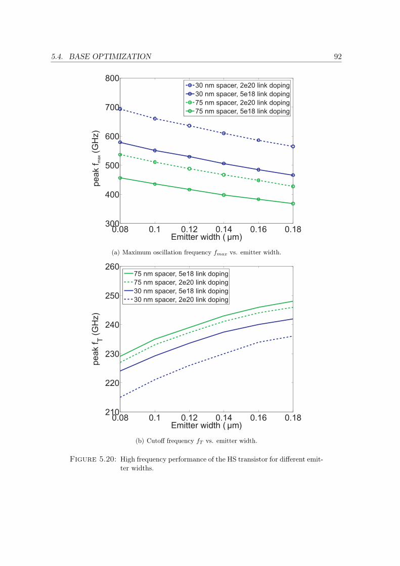
5.4. BASE OPTIMIZATION 92
0.08 0.1 0.12 0.14 0.16 0.18300
400
500
600
700
800
Emitter width ( μm)
peak
f ma
x(G
Hz)
30 nm spacer, 2e20 link doping
30 nm spacer, 5e18 link doping
75 nm spacer, 2e20 link doping
75 nm spacer, 5e18 link doping
(a) Maximum oscillation frequency fmax vs. emitter width.
0.08 0.1 0.12 0.14 0.16 0.18210
220
230
240
250
260
Emitter width ( μm)
peak
f T(G
Hz)
75 nm spacer, 5e18 link doping
75 nm spacer, 2e20 link doping
30 nm spacer, 5e18 link doping
30 nm spacer, 2e20 link doping
(b) Cutoff frequency fT vs. emitter width.
Figure 5.20: High frequency performance of the HS transistor for different emit-ter widths.
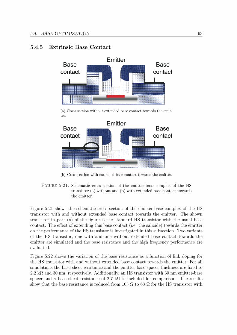
5.4. BASE OPTIMIZATION 93
5.4.5 Extrinsic Base Contact
SiGe base
Base
contact
EmitterBase
contact
SiGe base
Base
contact
EmitterBase
contact
(a) Cross section without extended base contact towards the emit-ter.
SiGe base
Base
contact
EmitterBase
contact
SiGe base
Base
contact
EmitterBase
contact
(b) Cross section with extended base contact towards the emitter.
Figure 5.21: Schematic cross section of the emitter-base complex of the HStransistor (a) without and (b) with extended base contact towardsthe emitter.
Figure 5.21 shows the schematic cross section of the emitter-base complex of the HStransistor with and without extended base contact towards the emitter. The showntransistor in part (a) of the figure is the standard HS transistor with the usual basecontact. The effect of extending this base contact (i.e. the salicide) towards the emitteron the performance of the HS transistor is investigated in this subsection. Two variantsof the HS transistor, one with and one without extended base contact towards theemitter are simulated and the base resistance and the high frequency performance areevaluated.
Figure 5.22 shows the variation of the base resistance as a function of link doping forthe HS transistor with and without extended base contact towards the emitter. For allsimulations the base sheet resistance and the emitter-base spacer thickness are fixed to2.2 kΩ and 30 nm, respectively. Additionally, an HS transistor with 30 nm emitter-basespacer and a base sheet resistance of 2.7 kΩ is included for comparison. The resultsshow that the base resistance is reduced from 103 Ω to 63 Ω for the HS transistor with
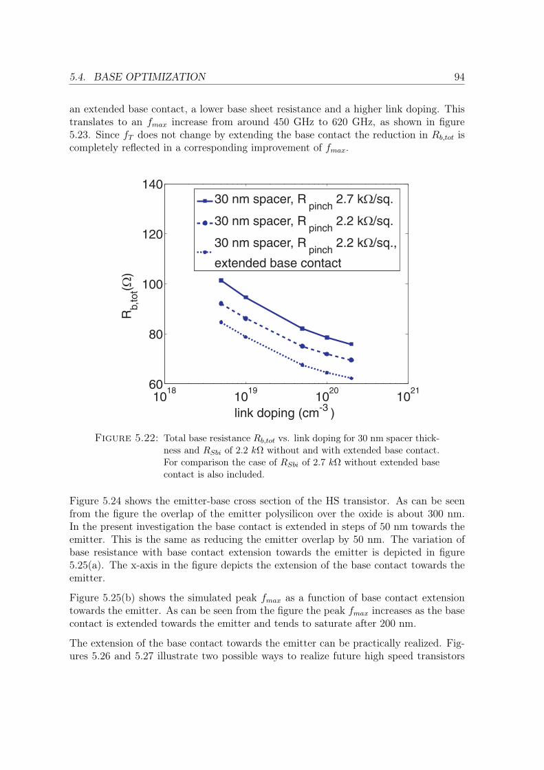
5.4. BASE OPTIMIZATION 94
an extended base contact, a lower base sheet resistance and a higher link doping. Thistranslates to an fmax increase from around 450 GHz to 620 GHz, as shown in figure5.23. Since fT does not change by extending the base contact the reduction in Rb,tot iscompletely reflected in a corresponding improvement of fmax.
1018
1019
1020
1021
60
80
100
120
140
link doping (cm-3
)
Rb,t
ot(
)�
30 nm spacer, Rpinch
2.7 k�/sq.
30 nm spacer, Rpinch
2.2 k�/sq.
30 nm spacer, Rpinch
2.2 k�/sq.,
extended base contact
Figure 5.22: Total base resistance Rb,tot vs. link doping for 30 nm spacer thick-ness and RSbi of 2.2 kΩ without and with extended base contact.For comparison the case of RSbi of 2.7 kΩ without extended basecontact is also included.
Figure 5.24 shows the emitter-base cross section of the HS transistor. As can be seenfrom the figure the overlap of the emitter polysilicon over the oxide is about 300 nm.In the present investigation the base contact is extended in steps of 50 nm towards theemitter. This is the same as reducing the emitter overlap by 50 nm. The variation ofbase resistance with base contact extension towards the emitter is depicted in figure5.25(a). The x-axis in the figure depicts the extension of the base contact towards theemitter.
Figure 5.25(b) shows the simulated peak fmax as a function of base contact extensiontowards the emitter. As can be seen from the figure the peak fmax increases as the basecontact is extended towards the emitter and tends to saturate after 200 nm.
The extension of the base contact towards the emitter can be practically realized. Fig-ures 5.26 and 5.27 illustrate two possible ways to realize future high speed transistors
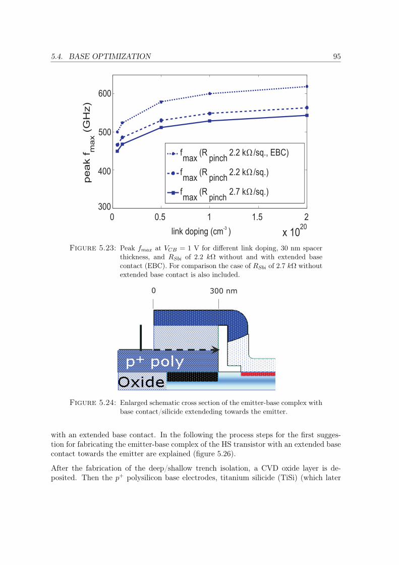
5.4. BASE OPTIMIZATION 95
0 0.5 1 1.5 2
x 1020
300
400
500
600
link doping (cm-3
)
peak
f ma
x(G
Hz)
fmax
(Rpinch
2.2 k� /sq., EBC)
fmax
(Rpinch
2.2 k� /sq.)
fmax
(Rpinch
2.7 k� /sq.)
Figure 5.23: Peak fmax at VCB = 1 V for different link doping, 30 nm spacerthickness, and RSbi of 2.2 kΩ without and with extended basecontact (EBC). For comparison the case of RSbi of 2.7 kΩ withoutextended base contact is also included.
0 300 nm
Figure 5.24: Enlarged schematic cross section of the emitter-base complex withbase contact/silicide extendeding towards the emitter.
with an extended base contact. In the following the process steps for the first sugges-tion for fabricating the emitter-base complex of the HS transistor with an extended basecontact towards the emitter are explained (figure 5.26).
After the fabrication of the deep/shallow trench isolation, a CVD oxide layer is de-posited. Then the p+ polysilicon base electrodes, titanium silicide (TiSi) (which later
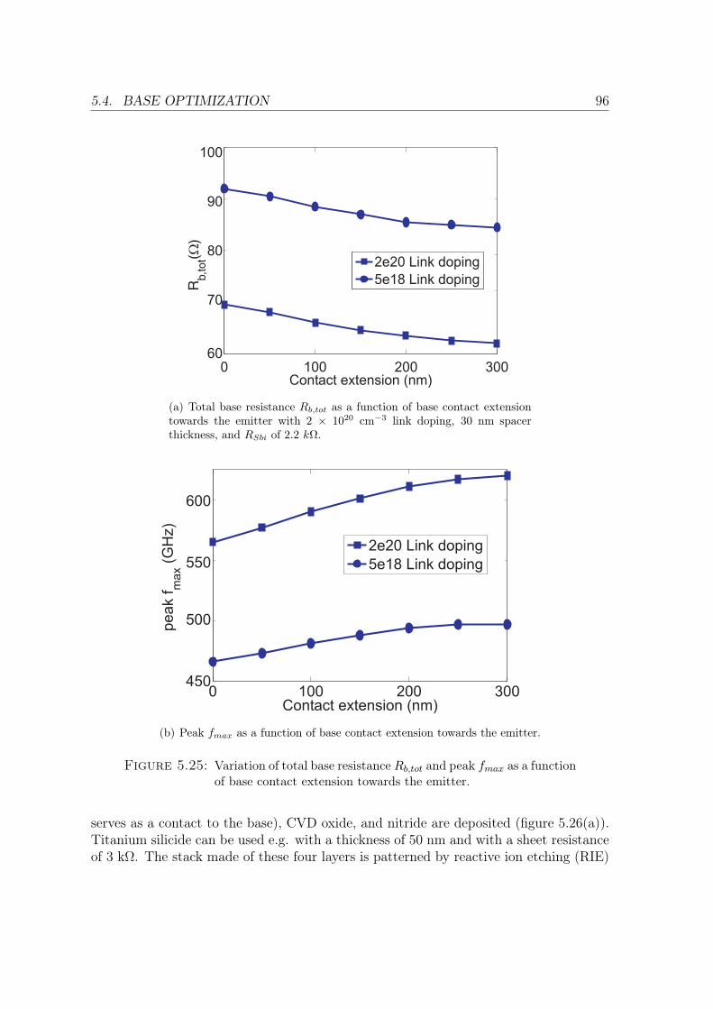
5.4. BASE OPTIMIZATION 96
0 100 200 300Contact extension (nm)
60
70
80
90
100
2e20 Link doping
5e18 Link dopingRb,t
ot(
)�
(a) Total base resistance Rb,tot as a function of base contact extensiontowards the emitter with 2 × 1020 cm−3 link doping, 30 nm spacerthickness, and RSbi of 2.2 kΩ.
0 100 200 300450
500
550
600
Contact extension (nm)
pe
ak
f max
(GH
z)
2e20 Link doping
5e18 Link doping
(b) Peak fmax as a function of base contact extension towards the emitter.
Figure 5.25: Variation of total base resistance Rb,tot and peak fmax as a functionof base contact extension towards the emitter.
serves as a contact to the base), CVD oxide, and nitride are deposited (figure 5.26(a)).Titanium silicide can be used e.g. with a thickness of 50 nm and with a sheet resistanceof 3 kΩ. The stack made of these four layers is patterned by reactive ion etching (RIE)
5.4. BASE OPTIMIZATION 97
for forming the emitter window (figure 5.26(b)). Then the processing of nitride spacers(figure 5.26(c)), CVD oxide removal for base deposition, base deposition by selectiveepitaxial growth, and formation of emitter (figure 5.26(d)) are done as described in sec-tion 2.5.2 of this work. The processing is completed by forming the contact holes andthe copper metallization (figure 5.26(e)). The final figure shows the HS transistor witha TiSi contact to the base extended towards the emitter.
Figure 5.27 shows the second suggestion to extend the base contact towards the emitter.Figures 5.27(a), 5.27(b), and 5.27(c) illustrate the HS transistor with an emitter overlapof 300 nm, 200 nm, and 100 nm, respectively. As can be seen from the figure the contactis extended towards the emitter by reducing the emitter overlap. In the standard HStransistor the overlap of the emitter polysilicon over the oxide is 300 nm. Practically, itis possible to reduce the emitter overlap down to 100 nm by using controlled lithographytechniques and so the advantage of the base contact extension towards the emitter foundby the simulations can be realized.
Figure 5.28 shows the 2006 update of the ITRS (International road map for semiconduc-tors) for the expected trends for fT and fmax versus the year of production. Accordingto the ITRS trend for fmax, this frequency is expected to reach 500 GHz by 2015. Withthe improvements and modifications investigated in this chapter in great detail it seemsfeasible that transistors in this performance range can be fabricated within the next fewyears based on existing technology concepts (i.e. without revolutionary breakthroughs).
There are further opportunities to improve the SiGe HBT performance significantly.Many processes available in CMOS have not yet been implemented in SiGe HBTs, suchas spike anneals or low barrier silicides, to name a few. Continued vertical scaling ofthe intrinsic device, however, will require new processes and materials.
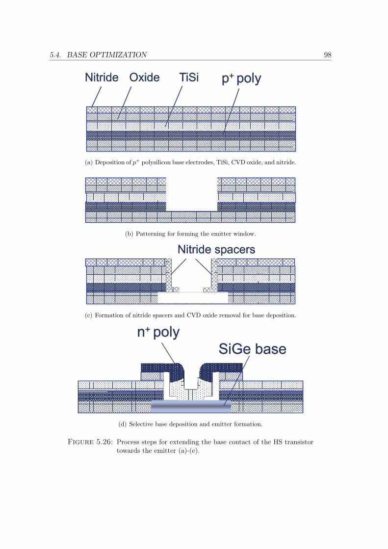
5.4. BASE OPTIMIZATION 98
Nitride Oxide TiSi p+ polyNitride Oxide TiSi p+ poly
(a) Deposition of p+ polysilicon base electrodes, TiSi, CVD oxide, and nitride.
(b) Patterning for forming the emitter window.
Nitride spacersNitride spacers
(c) Formation of nitride spacers and CVD oxide removal for base deposition.
SiGe base
n+ poly
SiGe base
n+ poly
(d) Selective base deposition and emitter formation.
Figure 5.26: Process steps for extending the base contact of the HS transistortowards the emitter (a)-(e).
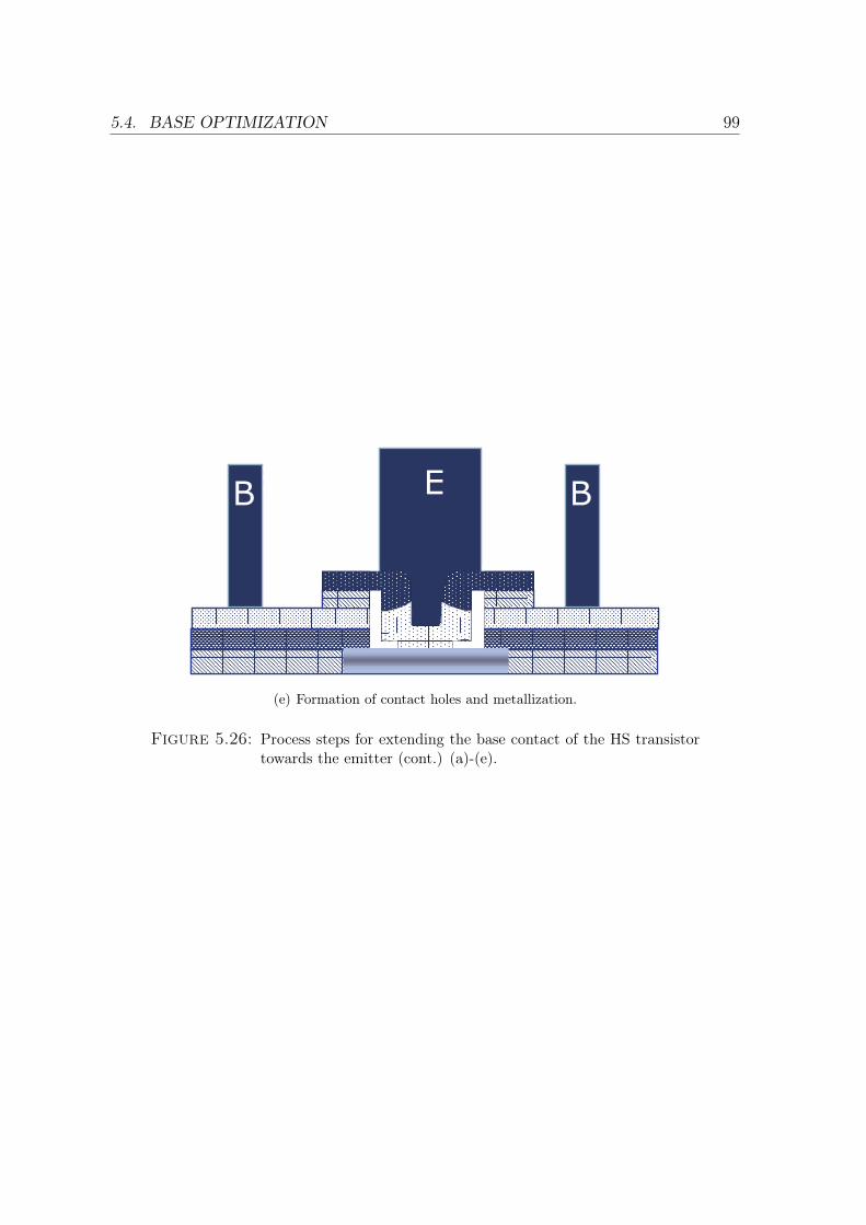
5.4. BASE OPTIMIZATION 99
B E BBB E BB
(e) Formation of contact holes and metallization.
Figure 5.26: Process steps for extending the base contact of the HS transistortowards the emitter (cont.) (a)-(e).
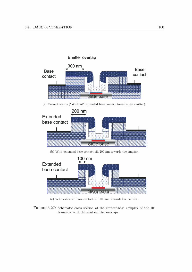
5.4. BASE OPTIMIZATION 100
SiGe base
Base
contact
Emitter overlap
Base
contact
300 nm
SiGe baseSiGe base
Base
contact
Emitter overlap
Base
contact
300 nm
SiGe base
(a) Current status ("Without" extended base contact towards the emitter).
SiGe base
Extended
base contact
200 nm
SiGe baseSiGe base
Extended
base contact
200 nm
SiGe base
(b) With extended base contact till 200 nm towards the emitter.
SiGe base
Extended
base contact
100 nm
SiGe baseSiGe base
Extended
base contact
100 nm
SiGe base
(c) With extended base contact till 100 nm towards the emitter.
Figure 5.27: Schematic cross section of the emitter-base complex of the HStransistor with different emitter overlaps.
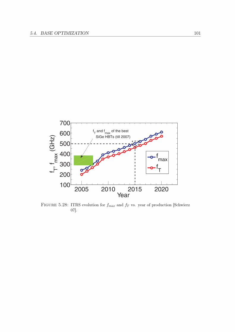
5.4. BASE OPTIMIZATION 101
2005 2010 2015 2020100
200
300
400
500
600
700
Year
f T,f m
ax
(GH
z)
fmax
fT
fT
and fmax
of the best
SiGe HBTs (till 2007)
Figure 5.28: ITRS evolution for fmax and fT vs. year of production [Schwierz07].
Chapter 6
Summary and Outlook
It is indispensable to base the development of a new microelectronic technology to alarge extent on simulations, because the corresponding experiments are extremely ex-pensive and time consuming. TCAD simulations therefore play a key role in competitivetechnology development and in obtaining a deep physical understanding of future gen-erations of high speed SiGe HBTs including a profound analysis of their physical andelectrical limits.
The team within this thesis was performed has developed the current generation of In-fineon’s high speed SiGe bipolar technology B7HF200 with transistors with a transitfrequency of 200 GHz and is now performing research for the next generation of fastSiGe HBTs. With B7HF200 a highly integrated chip for 77 GHz automotive radarapplication has been realized in close cooperation between product and technology de-velopment teams. This chip is the worldwide first Si based product for such a demandingapplication at this high operation frequency.
My part in this development was to perform all the device and process simulation workrequired for these developments, including its experimental verification by measure-ments on fabricated devices, which I had to perform autonomously. The first part ofthe thesis describes the optimization of a 200 GHz SiGe bipolar technology to enable77 GHz automotive radar applications. Beside the main device, i.e. a high speed npnbipolar transistor with a transit frequency of 200 GHz, a high voltage npn transistorand a varactor have been optimized by device and process simulation before the actualfabrication. These devices are important components for the realization of the radarproducts. By simulation the sensitivity of the varactor characteristics to the dopingprofile has been studied, thereby finding optimal process steps for reducing the electri-cal variations. For example, to obtain a hyper-abrupt profile with the required tuningratio and electrical parameter homogeneity, three phosphorus implants with differentdoses and energies are required. First compact model parameters of this varactor forevaluating the 77 GHz VCO circuit have been provided based on these varactor devicesimulations, and have been later verified by experiment.
102
6.1. SUMMARY OF RESULTS AND CONCLUSIONS 103
The second part of the thesis is concerned with investigations by detailed device simula-tions towards the next generation of SiGe high speed npn transistors with considerablehigher performance in terms of operation frequency. Such devices will open applicationsat higher frequencies, or will improve performance and power consumption of systemsat a given frequency. This work includes the investigation of the necessary advancedconcepts guided by the practical boundaries and limitations given by the experts ofthe various sophisticated fabrication processes. These detailed studies have providedthe most promising approaches for the next generation of SiGe bipolar transistors. Ithas been found that transistors with maximum oscillation frequencies above 500 GHzshould be feasible. The experimental realization of such devices is currently performedin a large European project called DOTFIVE (www.dotfive.eu).
The large number of results achieved during the investigations required for all thesechallenging tasks of this thesis are detailed in the following section.
6.1 Summary of Results and Conclusions
First a new process concept ("double epitaxy") is proposed for simultaneously opti-mizing the high speed transistor independent of the high voltage transistor on the samechip. Using the new concept the degree of freedom for improving the performance of theHS transistor without degrading the breakdown voltage of the HV transistor is signif-icantly increased. This concept provides the maximum degree of freedom for realizingtransistors with different fT -BVCEO trade-offs on one chip. Using this concept a HStransistor with a cutoff frequency fT greater than 200 GHz, a maximum oscillation fre-quency fmax of 237 GHz, and an open base collector-emitter breakdown voltage BVCEO
of 1.8 V along with a HV transistor with an fT of 52 GHz, fmax of 175 GHz, and BVCEO
of 5 V are integrated on the same chip. In comparison to the previous approach usinga single epitaxial growth, the results show that by using the double epitaxy concept,an increase of BVCEO from 3.2 V to 5 V and of the collector-base breakdown voltageBVCBO from 10.5 V to 17 V is obtained for the HV transistor while maintaining the sameperformance of the HS transistor. This process concept has been investigated by 2-Ddevice simulations and has then been realized by extending the previous production pro-cess accordingly. The simulated results are compared with the measured results. Goodagreement for simulation and measurement is obtained for the HS and HV transistors.
Additionally, using the ’double epitaxy’ concept, a varactor suitable for 77 GHz radarapplications has been investigated and developed by means of 1-D process and devicesimulations. Using the new concept the characteristics of the varactor and the per-formance of the HS transistors can be decoupled from each other and can thereforebe independently optimized. Optimum profiles for the varactor for achieving sufficientcapacitance tuning ratio and acceptable quality factor for the application under con-sideration (77 GHz automotive radar) are found by process simulations and electricalparameters for the varactor are extracted from device simulations. Simulation results
6.1. SUMMARY OF RESULTS AND CONCLUSIONS 104
showed an improvement in the varactor characteristics and thereby the VCO tuningrange for the optimized varactor profiles with the new concept. A varactor has beenfabricated with these optimized profiles. The capacitance tuning ratio between 0 V and5 V for the fabricated varactor is about 2.3. At 50 GHz and for a tuning voltage of5 V, the quality factor is around 16, and reduces to about 6.5 for a tuning voltage of0 V. The achieved tuning ratio and the quality factor are found to be sufficient for thechallenging application under consideration (77 GHz automotive radar). Therefore aVCO suitable for 77 GHz automotive radar applications has been realized with the newvaractor. It has been found that the tuning range of the VCO with the new varactor hasincreased from 7 GHz to 13 GHz at almost the same phase noise performance comparedto the VCO with the base-collector diode of a HS transistor for capacitor tuning, asused previously.
After this various optimizations of the emitter, base, and collector for further enhancingthe performance of the HS transistor have been studied. As a part of emitter optimiza-tion, it has been found that by using a relatively simple un-doped silicon cap instead ofthe conventional p-doped silicon cap the cutoff frequency fT increases by 15 GHz (10%). This is verified by simulation and experiment. Therefore, the existing technologythat used a p-doped silicon cap was changed to incorporate an un-doped silicon cap.It has also been found that using an un-doped silicon cap and additionally reducingthe silicon cap thickness will result in a further increase of the performance of the HStransistor.
With the above described ’double epitaxy’ concept, the optimization of the collectorin terms of fT can be done independently from the HV transistor. Therefore, differentcollector optimizations of the HS transistor like increasing the collector doping for en-hanced fT and reducing the collector epitaxy thickness have been investigated by meansof 2-D device simulations. The results show that for a HS transistor with a thin col-lector thickness of 40 nm and a high collector doping of 1.5 × 1018 cm−3 fT increasesfrom 176 GHz to 287 GHz compared to the HS transistor with a collector thickness of120 nm and a collector doping of 5 × 1017 cm−3. For the standard HS transistor of thepresent technology (120 nm collector thickness, 1 × 1018 cm−3 collector doping) thismeans that by reducing the collector thickness to 40 nm and increasing the doping to1.5 × 1018 cm−3 an improvement in cutoff frequency of 45 GHz can be achieved.
Finally different approaches for reducing the total base resistance and thereby for im-proving the maximum oscillation frequency of the device have been investigated. Theseapproaches are investigated extensively by 2-D device simulations. It has been foundthat the base resistance reduction plays the major role for improving the current HStransistor towards the next generation. A huge potential for base resistance reductionhas been identified by emitter-base spacer thickness reduction, base contact/silicide ex-tension towards the emitter, higher link region doping, intrinsic base sheet resistancereduction, and laterally scaling the emitter dimensions. The simulations show that ahigh speed transistor with a thin emitter-base spacer of 30 nm, an extended base contacttowards the emitter, an increased link doping of 2 × 1020 cm−3, a reduced RSbi of 2.2
6.2. OUTLOOK - SUGGESTIONS FOR FUTURE WORK 105
kΩ/�, and a thin emitter width of 80 nm increases the maximum oscillation frequencyof the actual transistors from 340 GHz to 700 GHz, doubling the present performance.For realizing the extended base contact towards the emitter process concepts have beensuggested in this work, the other improvements can be already implemented by usingstate-of-the-art process technology.
6.2 Outlook - Suggestions for Future Work
With the investigated optimizations and modifications of the high speed transistor itseems feasible that transistors, which have almost twice the maximum oscillation fre-quency compared to today, can be fabricated within the next few years based on existingtechnology concepts (i.e. without revolutionary breakthroughs). The aim of the Eu-ropean project DOTFIVE (www.dotfive.eu) is to experimentally realize devices withsuch high operating speeds. One important future step that is closely related to thiswork is again the verification and calibration of the performed simulations after the firsthardware results of these devices are available. These devices will directly lead to im-proved automotive radar systems with higher performance at lower power consumptionthereby increasing road safety and energy budget. This also leads to reduced coolingeffort, which reduces packaging costs.
Besides improving the performance of existing circuits, the availability of faster tran-sistors will also open new application fields for silicon based integrated systems. Manyoptically opaque materials are transparent to terahertz (THz) radiation, and deviceswith maximum oscillation frequencies of 0.5 THz and above will enable new sensing andimaging possibilities in various areas of science and technology [Maagt 05]. An impor-tant example can be imaging for security purposes e.g. at airports or other sensitivelocations.
Since in this work the base link region, which establishes the connection between theintrinsic SiGe base and the p+-polysilicon base electrodes, is identified as the majorperformance limiting region, special attention will have to be devoted to it. Detailedinvestigations of more advanced concepts for this link region will be in focus.
Related to the future simulation work it will be important to consider that we arealready dealing with base widths in the nanometer range. It is obvious that we areentering a region where physical effects at the atomic level, non-local and quasi-ballisticcarrier transport in the base and BC space charge region, and barrier related effects dueto the sharper doping and material profiles will become more important. Furthermoreelectrothermal effects, caused by higher current densities and fields within the devices,and coupling between devices will have increased influence. They are not sufficientlycovered by the compact models in the current simulation tools. Hence an importantfuture task will be to identify the most important of these effects and to incorporatethem in an adequate TCAD platform for the next generation.
Bibliography
[Alamo 87] J. A. Del Alamo and R. M. Swanson, “Measurement of steady-stateminority-carrier transport parameters in heavily doped n-type silicon”,IEEE Trans. Electron Devices, vol. 34, pp. 1580–1589, March 1987.
[Armstrong 07] G. A. Armstrong and C. A. Maiti, TCAD for Si, SiGe and GaAs inte-
grated circuits, U.K.: Stevenage Herts, 2007.
[Ashburn 88] P. Ashburn, Design and realization of bipolar transistors, Chichester:Wiley, 1988.
[Böck 04,a] J. Böck, H. Schäfer, H. Knapp, K. Aufinger, M. Wurzer, S. Boguth,T. Böttner, W. Perndl, and T. F. Meister, “3.3 ps SiGe bipolar tech-nology”, IEDM Tech. Dig., pp. 255–258, IEEE, December 2004.
[Böck 04,b] J. Böck, H. Schäfer, K. Aufinger, R. Stengl, S. Boguth, R. Schreiter,M. Rest, H. Knapp, M. Wurzer, W. Perndl, T. Böttner, andT. F. Meister, “SiGe bipolar technology for automotive radarapplications”, BCTM Tech. Dig., pp. 84–87, IEEE, September 2004.
[Braunstein 58] R. Braunstein, A. R. Moore, and F. Herman, “Intrinsic optical absorp-tion in germanium-silicon alloys”, Phys. Rev., vol. 109, pp. 695–710,December 1958.
[Bufler 97] F. M. Bufler, P. Graf, B. Meinerzhagen, B. Adeline, M. M. Rieger,H. Kibbel, and G. Fischer, “Low and high-field electron-transport pa-rameters for unstrained and strained Si1−xGex”, IEEE Electron Device
Letters, vol. 18, pp. 264–266, 1997.
[Burghartz 97] J. N. Burghartz, M. Soyuer, K. A. Jenkins, M. Kies, M. Dolan, K.J. Stein, J. Malinowski, and D. L. Harame, “Integrated RF componentsin a SiGe bipolar technology”, IEEE Journal of Solid-State Circuits,vol. 32, pp. 1440–1445, 1997.
[Caughey 67] D. M. Caughey and R. E. Thomas, “Carrier mobilities in silicon em-pirically related to doping and field”, Proceedings of the IEEE, vol. 55,pp. 2192–2193, 1967.
106
BIBLIOGRAPHY 107
[Chevalier 05] P. Chevalier, C. Fellous, L. Rubaldo, F. Pourchon, S. Pruvost,R. Beerkens, F. Saguin, S. Lepilliet, D. Celi, I. Telliez, D. Gloria,F. Aniel, F. Danneville, and A. Chantre, “230-GHz self-aligned SiGeCHBT for optical and millimeter-wave applications”, IEEE Journal of
Solid-State Circuits, vol. 40, pp. 2025–2034, October 2005.
[Cressler 03] J. D. Cressler and G. Niu, Silicon-germanium heterojunction bipolar
transistors, Artech House, 2003.
[Cressler 05] J. D. Cressler, The silicon heterostructure handbook: Materials, fabri-
cation, devices, circuits, and applications of SiGe and Si strained layer
epitaxy, CRC Press, 2005.
[Donkers 07] J. J. T. M. Donkers, M. C. J. C. M. Kramer, H. van Huylenbroeck, L. JChoi, P. Meunier-Bernard, A. Sibaja-Hernandez, G. Boccardi, W. vanNoort, G. A. M. Hurkx, T. Vanhoucke, F. Vleugels, G. Winderickx,E. Kunnen, S. Peeters, D. Baute, B. De Vos, T. Vandeweyer, R. Loo,R. Venegas, R. Pijper, F. C. Voogt, S. Decoutere, and E. A. Hijzen, “Anovel fully self-aligned SiGe:C HBT architecture featuring a single-stepepitaxial collector-base process”, IEDM Tech. Dig., pp. 655–658, IEEE,December 2007.
[Ershov 94] M. Ershov and V. Ryzhii, “High-field electron transport in SiGe alloy”,J. Appl. Phy., vol. 33, pp. 1365–1371, 1994.
[Fischetti 96] M. V. Fischetti and S. E. Laux, “Band structure, deformation poten-tials, and carrier mobility in strained Si, Ge, and SiGe alloys”, J. Appl.
Phys., vol. 80, pp. 2234–2252, August 1996.
[Floyd 06] B. Floyd, S. Reynolds, U. R. Pfeiffer, T. Beukema, J. Grzyb, and C.Haymes, “A silicon 60 GHz receiver and transmitter chipset for broad-band communications”, Int. Solid-State Circ. Conf., pp. 184–185, IEEE,February 2006.
[Hajimiri 05] A. Hajimiri, H. Hashemi, A. Natarajan, X. Guan, and A. Komijani,“Integrated phased array systems in silicon”, Proceedings of the IEEE,vol. 93, pp. 1637–1654, September 2005.
[Harame 95] D. L. Harame, J. H. Comfort, J. D. Cressler, E. F. Crabbe, J. Y. -C.Sun, B. S. Meyerson, and T. Tice, “Si/SiGe epitaxial base transistors-part I: Materials, physics, and circuits”, IEEE Trans. Electron Devices,vol. 42, pp. 455–468, March 1995.
[Infineon 05] Infineon and Lucent, Abschlussbericht zum BMBF-Verbundprojekt
"Höchstperformante SiGe-Technologien für High-Speed-
Kommunikationsnetze", Infineon, 2005.
BIBLIOGRAPHY 108
[ITRS 06] ITRS, 1999, 2001, 2003, 2005 edition. Update 2006, SemiconductorIndustry Association, 2006.
[Iyer 87] S. S. Iyer, G. L. Patton, S. L. Delage, S. Tiwari, and J. M. C. Stork,“Silicon-germanium base heterojunction bipolar transistors by molecu-lar beam epitaxy”, IEDM Tech. Dig., pp. 874–876, IEEE, September1987.
[Katayama 07] Y. Katayama, C. Haymes, D. Nakano, T. J. Beukema, B. Gaucher, andK. Schleupen, “2-Gbps uncompressed HDTV transmission over 60-GHzSiGe radio”, IEEE Consumer Communications and Networking Conf.,pp. 12–16, IEEE, January 2007.
[Kenneth 98] K. O Kenneth and W. B. Scharf, “Effects of buried layer geometry oncharacteristics of double polysilicon bipolar transistors”, IEEE Electron
Device Letters, vol. 19, pp. 160–162, 1998.
[King 89] C. A. King, J. L. Hoyt, and J. F. Gibbons, “Bandgap and transportproperties of Si1−xGex by analysis of nearly ideal Si/Si1−xGex/Si he-terojunction bipolar transistors”, IEEE Trans. Electron Devices, vol.36, pp. 2093–2104, December 1989.
[Kirk 62] C. T. Kirk, “A theory for transistor cutoff frequency (fT ) falloff at highcurrent densities.”, IEEE Trans. Electron Devices, vol. 9, pp. 164–174,1962.
[Klaassen 92,a] D. B. M. Klaassen, “A unified mobility model for device simulation I.Model equations and concentration dependence”, Solid-State Elec., vol.35, pp. 953–960, July 1992.
[Klaassen 92,b] D. B. M. Klaassen, “A unified mobility model for device simulation II.Temperature dependence of carrier mobility and lifetime”, Solid-State
Elec., vol. 35, pp. 961–967, July 1992.
[Kritivasan 06] R. Kritivasan, Y. Lu, J. D. Cressler, J. S. Rieh, M. Khater, D. Ahlgren,and G. Freeman, “Half-terahertz operation of SiGe HBTs”, IEEE Trans.
Electron Devices, vol. 27, pp. 567–569, July 2006.
[Krömer 57] H. Krömer, “Theory of a wide-gap emitter for transistors”, Proceedings
of the IRE, vol. 45, pp. 1535–1537, 1957.
[Lang 85] D. V. Lang, R. People, J. C. Bean, and A. M. Sergent, “Measurementof the band gap of Si1−xGex/Si strained-layer heterostructures”, Appl.
Phys. Lett., vol. 47, pp. 1333–1335, December 1985.
BIBLIOGRAPHY 109
[Li 04] H. Li, H. M. Rein, T. Suttorp, and J. Böck, “Fully integrated SiGeVCOs with powerful output buffer for 77-GHz automotive radar sys-tems and applications around 100 GHz”, IEEE Journal of Solid-State
Circuits, vol. 39, pp. 1650–1658, October 2004.
[Liu 05] Q. Z. Liu, B. A. Orner, L. Lanzerotti, M. Dahlstrom, W.Hodge,M. Gordon, J. Johnson, M. Gautsch, J. Greco, J. Rascoe, D. Ahlgren,A. Joseph, and J. Dunn, “SiGe HBT technology with fmax/fT =350/300 GHz and gate delay below 3.3 ps”, Proceedings of Compound
Semiconductor Integrated Circuit Symposium, pp. 117–120, IEEE, Oc-tober 2005.
[Maagt 05] P. de Maagt, P. H. Oliver, and C. Mann, Terahertz science, engineering
and systems - from space to earth applications, John Wiley and Sons,2005.
[Matthews 74] J. W. Matthews and A. E. Blakeslee, “Defects in epitaxial multilayers:I. Misfit dislocations in layers”, J. Cryst. Growth, vol. 27, pp. 118–125,1974.
[Matthews 75] J. W. Matthews, “Defects associated with the accomodation of misfitbetween crystals”, J. Vac. Sci. Technol., vol. 22, pp. 1696–1710, 1975.
[MEDICI 06] TMA MEDICI, Two-dimensional device simulation program, VersionY-2006.06 user’s manual, 2006.
[Meister 03] T. F. Meister, H. Schäfer, K. Aufinger, R. Stengl, S. Boguth,R. Schreiter, H. Knapp, M. Wurzer, A. Mitchell, T. Böttner, andJ. Böck, “SiGe Bipolar technology with 3.9 ps gate delay”, BCTM
Tech. Dig., pp. 103–106, IEEE, September 2003.
[Meyer 87] R. G. Meyer and R. S. Muller, “Charge-control analysis of the collector-base space-charge-region contribution to bipolar transit time constantτt”, IEEE Trans. Electron Devices, vol. 34, pp. 450–452, 1987.
[Michael 02] G. J. Michael and G. Mike, RF and Microwave Semiconductor Device
Handbook, CRC Press, 2002.
[Moll 56] J. Moll and I. Ross, “The dependence of transistor parameters on thedistribution of base layer resistivity”, Proceedings of the IRE, vol. 44,pp. 72–78, January 1956.
[Ng 95] K. Ng, Complete guide to semiconductor devices, McGraw-Hill, 1995.
[Olesinski 84] J. W. Olesinski and G. J. Abbaschian, “The Ge-Si (Germanium-Silicon)system”, Bulletin of Alloy Phase Diagrams, vol. 5, pp. 180–183, 1984.
BIBLIOGRAPHY 110
[Penfield 62] P. Penfield and R. P. Rafuse, Varactor applications, Cambridge: M.I.TPress, 1962.
[People 85] R. People, “Indirect band gap of coherently strained GexSi1−x bulkalloys on (0 0 1) silicon substrates”, Phys. Rev. B, vol. 32, pp. 1405–1408, December 1985.
[People 86,a] R. People, “Physics and applications of GexSi1−x/Si strained layer het-erostructures”, IEEE Journal of Quantum Elect., vol. 22, pp. 1696–1710, March 1986.
[People 86,b] R. People and J. C. Bean, “Band alignments of coherently strainedGexSi1−x/Si on (0 0 1) GeySi1−y/Si substrates”, Appl. Phys. Letters,vol. 48, pp. 1405–1408, December 1986.
[Pritchard 55] R. L. Pritchard, “High-frequency power gain of junction transistors”,Proceedings of the IRE, vol. 43, pp. 1075–1085, December 1955.
[Reisch 03] M. Reisch, High-frequency bipolar transistors, Springer-Verlag, 2003.
[Rieh 02] J. S. Rieh, B. Jagannathan, H. Chen, K. T. Schonenberg, D. Angell,A. K. Chinthakindi, J. Florkey, F. Golan, D. Greenberg, S.−J. Jeng,M. Khater, F. Pagette, C. Schnabel, P. Smith, A. Stricker, K.Vaed,R. Volant, D. Ahlgren, G. Freeman, K. J. Stein, and S. Subbanna, “SiGeHBTs with cutoff frequency of 350 GHz”, IEDM Tech. Dig., pp. 771–774, IEEE, December 2002.
[Rieh 04] J. S. Rieh, M. Khater, T. Adam, A. Chinthakindi, J. Johnson, R. Kr-ishnasamy, M. Meghelli, F. Pagette, D. Sanderson, C. Schnabel, K.T. Schonenberg, P. Smith, K. Stein, and G. Freeman, “SiGe HBT tech-nology with fmax/fT = 350/300 GHz and gate delay below 3.3 ps”,IEDM Tech. Dig., pp. 247–250, IEEE, December 2004.
[Roulston 90] D. J. Roulston, Bipolar semiconductor devices, Singapore: McGrawHill, 1990.
[Sansen 72] W. M. C. Sansen and R. G. Meyer, “Characterization and Measurementof the Base and Emitter Resistances of Bipolar Transistors”, Solid-State
Elec., vol. 7, pp. 492–498, 1972.
[Schwerd 03] M. Schwerd, M. Seck, T. Huttner, T. Böttner, S. Drexl, B. Hasler,A. Mitchell, H. Helneder, H. Körner, V. Kubrak, M. Schrenk, and R.Lachner, “A manufacturable 0.35 μm 150 GHz fT SiGe:C bipolar RFtechnology”, Proceedings of the Topical Meeting on Silicon Monolithic
Integrated Circuits in RF Systems, pp. 10–13, 2003.
[Schwierz 07] F. Schwierz and J. J. Liou, “RF Transistors: Recent developments androadmap toward terahertz applications”, Solid-State Elec., vol. 51, pp.1079–1091, July 2007.
[Selberherr 84] S. Selberherr, Analysis and simulation of semiconductor devices, Vi-enna: Springer-Verlag, 1984.
[Shi 03] Y. Shi, G. Niu, J. D. Cressler, and D. L. Harame, “On the consistentmodelling of bandgap narrowing for accurate device-level simulation ofscaled SiGe HBTs”, IEEE Trans. Electron Devices, vol. 50, pp. 1370–1377, 2003.
[Shockley 51] W. Shockley, U.S. Patent 2,569,347, 1951.
[Singh 93] J. Singh, Physics of semiconductors and their heterostructures,McGraw-Hill, 1993.
[Slotboom 76] J. W. Slotboom and H. C. De Graaff, “Measurements of bandgap nar-rowing in Si bipolar transistors”, Solid-State Elect., vol. 19, pp. 857–862,March 1976.
[Smith 80] P. Smith, M. Inoue, and J. Frey, “Electron velocity in Si and GaAs atvery high electric fields”, Appl. Phys. Lett, vol. 37, pp. 797–798, 1980.
[Sze 81] S. M. Sze, Physics of semiconductor devices, New York: McGraw-Hill,1981.
[Taur 98] Y. Taur and G. H. Ning, Fundamentals of modern VLSI devices, NewYork: Cambridge University Press, 1998.
[Tummala 08] R. Tummala, Introduction to system-on-package, New York: McGraw-Hill, 2008.
[Vytla 06] R. K. Vytla, T. F. Meister, K. Aufinger, D. Lukashevich, S. Boguth,H. Knapp, J. Böck, H. Schäfer, and R. Lachner, “Simultaneous inte-gration of SiGe high speed transistors and high voltage transistors ”,BCTM Tech. Dig., pp. 1–4, IEEE, October 2006.
[Weng 92] J. Weng and T. F. Meister, “New Method to determine the base resis-tance of bipolar transistors”, IEEE Electron Device Lett., vol. 13, pp.158–160, March 1992.
[Wong 00] W. M. Y. Wong, P. S. Hui, C. Zhiheng, S. Keqiang, J. Lau, andP. C. H. Chan, “A wide tuning range gated varactor”, IEEE Journal of
Solid-State Circuits, vol. 35, pp. 773–779, 2000.
111
Curriculum Vitae
Personal Details
Name and Surname Rajeev Krishna Vytla
Address Chiemgaustraße 131, 81549 MünchenDate and Place of Birth 13. August 1979 in Angara / IndiaNationality Indian
Home Address Ratna Residency, Flat F2, 10-3-11Ramaraopet, Kakinada 533007IndiaTel: +49 (0) 1799407093E-mail: [email protected]
Education
2005 - 2009 Doctorate Study
University of Bremen / Infineon Technologies AGDoctorate Thesis: "Physical Simulation of Advanced SiGe He-terojunction Bipolar Transistors"
2003-2004 Master Study in Electrical EngineeringUniversity of BremenMaster Thesis: "MOS-Controllable Diode for 6.5 kV TractionApplications"
1997 - 2001 Bachelor Study in Electrical Engineering (passed with dis-tinction)University of Madras, IndiaBachelor Thesis: "Secure Communication Using FDMA"
112