physical implementation - university of california,...
TRANSCRIPT

CS250, UC Berkeley Fall ‘09Lecture 08, Layout 1
CS250 VLSI Systems Design
Physical Implementation
Fall 2009
John Wawrzynek, Krste Asanovic’, with John Lazzaro
CS250, UC Berkeley Fall ‘09Lecture 08, Layout
OutlineStandard cell “back-end” place and route tools make layout mostly automatic. However, you should understand some of the more difficult concerns for physical implementation:
‣ Power distribution‣ Chip input/output ‣ Clock distribution‣ Floor-planning
‣ Not: Place & Route
2

CS250, UC Berkeley Fall ‘09Lecture 08, Layout 1
Routing PWR and GND‣ Main Design Concerns:
1. IR Drops. Remembering Ohms Law V = IR .
Voltage drops due to resistance in power/GND wires ⇒ slower circuits, false switching
2. Metal Migration (electromigration).Accidental fusing ⇒ chip failure
3. Inductive Effects. Bounce and oscillation on power nodes ⇒ false switching
3
CS250, UC Berkeley Fall ‘09Lecture 08, Layout 1
Metal Migration‣ A current flux through a metal conductor
exceeding a certain limit causes metal atoms to move in the direction of the current.
‣ If there is a small constriction ...
‣ the current density will be higher and more metal atoms will be carried away, creating a higher current density, ..., ⇒ open circuit
‣ Metal migration begins at ∼2x10⁵ A/cm2
‣ Design Guideline: Size width of both Vdd and GND wires so that no more than ∼0.5mA/um in width (aluminum).
4
Defect (or design)
like a fuse
CS250, UC Berkeley Fall ‘09Lecture 08, Layout 1
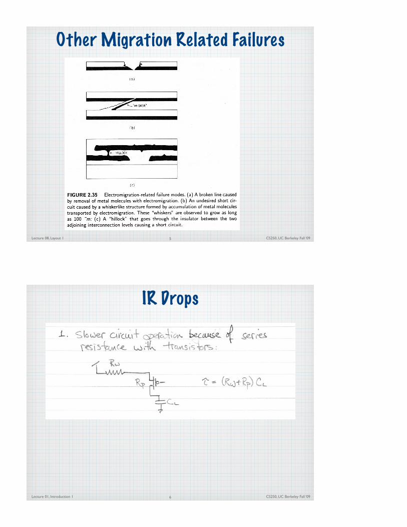
Other Migration Related Failures
5
CS250, UC Berkeley Fall ‘09Lecture 01, Introduction 1
IR Drops
6

CS250, UC Berkeley Fall ‘09Lecture 08, Layout 1
IR Drops
7
‣ Switching induced noise on pwr and GND rails can couple through to logic signals and cause accidental switching.
‣ Particularly troublesome around circuit with low noise immunity. Ex: RAM block sense amplifiers.
CS250, UC Berkeley Fall ‘09Lecture 08, Layout 1
Layout Strategy for Power Rails (power and ground wires)
1. Keep distance from source of power as short as possible.
2. Use wide/thick metal.3. Isolate “noisy” sections.4. Use multiple sources.
8

CS250, UC Berkeley Fall ‘09Lecture 08, Layout 1
Layout Strategy for Power Rails (power and ground wires)
‣ With many layers of metal, upper few layers are typically thicker than lower layers.
‣ Upper layers get allocated for global power rails.‣ Via connections to lower layers for local distribution.
9
CS250, UC Berkeley Fall ‘09Lecture 01, Introduction 1
Inductive Bounce
Inductance in the power and ground paths results in voltage glitches (noise) on Vdd and GND nodes.On-chip L values of wires is small => usually not significant except:
1. Very large currents: clock drivers, off-chip drivers2. Package pins, bonding wires (1nH/mm)
Package pins can have from 2-40nH of inductance, depending on package type
Strategy:1. Use multiple bonding pads (wires) from Vdd & GND2. If necessary, use on-chip bypass capacitors
10

CS250, UC Berkeley Fall ‘09Lecture 08, Layout 1
On-chip Bypass Capacitors
‣ When transistors switch, current is drawn from CD rather than through package pins and bonding wires - smoothes out dI/dt. (Think of it as a “charge cache”).
‣ Gate oxide leads to highest capacitance, but poor yield. Thicker oxides are used.
11
CS250, UC Berkeley Fall ‘09Lecture 08, Layout 1
On-chip Bypass Capacitance‣ Distributed bypass capacitors also smooth out noise from IR drops
by locally supplying charge when needed.
‣ Generally, capacitance on Vdd and GND is a good thing. (Fat wires help, larger transistor source regions help, extra capacitors when needed)
‣ Capacitive bypassing continues all the way up the packaging chain.
12

CS250, UC Berkeley Fall ‘09Lecture 08, Layout 1
Bypass Capacitors‣ On-chip bypass capacitors are not effective for off-chip drivers:
‣ On-chip capacitors keep the voltage difference across the power lines stable but cannot prevent the on-chip power-supply levels from moving up and down w.r.t. the board power-supply levels.
‣ Therefore, high-speed chip outputs are surrounded by many pwr and ground connections (pins). Example GTPs on Xilinx FPGAs, Memory interface on processors and bridge chips.
13
CS250, UC Berkeley Fall ‘09Lecture 08, Layout 1
Package Connections‣ “Pads”: Special cells in the “design kit” for the layout generator.
‣ Classic example of large capacitive fan-out. Internal capacitances on order of femto-farads, external ones are pico-farads. Uses staged drivers.
14
pad
circuitry
Pad (metal layer build-up), for wire bonding or
solder-ball
Circuitry provides ESD protection, drive strength
for output, input buffering, registering of signals, etc.
Vdd
GND
100um200um

CS250, UC Berkeley Fall ‘09Lecture 08, Layout 1
Electro-static Discharge (ESD) and Over-voltage Protection
15
CS250, UC Berkeley Fall ‘09Lecture 08, Layout 1
I/O Floorplan
‣ Signals get routed from chip core to periphery.
‣ Perimeter ∝ sqrt(area)
‣ At 200um pitch => 100 pads max per side (2cm die)
‣ Most commonly used for wire bond attachment.
16
“Perimeter” pads is the classic arrangement.

CS250, UC Berkeley Fall ‘09Lecture 08, Layout 1
I/O Floorplan
‣ Allow up to thousands of connections.
‣ Wire-bonding no longer possible => “flip-chip” technologies.
17
Area pads allow higher number of connections.
CS250, UC Berkeley Fall ‘09Lecture 08, Layout 1
Flip-chip Bonding‣ In addition to higher
density, lower resistance and inductance.
‣ Eases layout of circuits and power/clk distribution (signals come-in/go-out closer to where needed)
18
2 www.xilinx.com XAPP426 (v1.3) March 3, 2006
Implementing Xilinx Flip-Chip BGA PackagesR
*Xilinx flip-chip packages are not hermetically sealed and exposure to cleaning solvents/ chemicals or excessive moisture during boards assembly could pose serious package reliability concerns. Small vents are kept by design between the heatspreader (lid) and the organic substrate to allow for outgassing and moisture evaporation. Solvents or other corrosive chemicals could seep through these vents and attack the organic materials and components inside the package and hence are strongly discouraged during board assembly of Xilinx flip-chip BGA packages.
Recommended PCB Design Rules
For Xilinx BGA packages, NSMD (Non Solder Mask Defined) pads on the board are suggested. This allows a clearance between the land metal (diameter L) and the solder mask opening (diameter M) as shown in Figure 3. The space between the NSMD pad and the solder mask, and the actual signal trace widths depends on the capability of the PCB vendor. The cost of the PCB is higher when the line widths and spaces are tighter.
Figure 2: Package Construction with Type II Lid
Copper Heatspreader
Solder Ball
Flip Chip Solder Bump
Organic Build-Up Substrate
Underfill Epoxy
Silicon Die
Thermal Interface Material
Adhesive Epoxy*
Figure 3: Suggested Board Layout of Soldered Pads for BGA

CS250, UC Berkeley Fall ‘09Lecture 08, Layout 1
Clock Distribution
19
A challenging consequence of the synchronize design methodology is a need to distribute a clock signal in synchrony
to every state element - and do so with low-power (this challenge has driven some to asynchronous circuit design).
clock skew, delay in distribution
CLK
CLK’
Clock skew can create both setup and hold
problems.
CS250, UC Berkeley Fall ‘09Lecture 08, Layout 1
Clock Skew Related Failure
‣ If clock period T = TCL+Tsetup+Tclk→Q+Tskew, circuit will fail with setup time violation.‣ This problem can be fixed by increasing the clock period.
‣ If TCL < Tskew, circuit will fail with hold time violation.‣ Increasing the clock period will not help. Need to add delay.
20
CL
CLKCLK’
clock skew, delay in distribution
CLK
CLK’
CL
CLK
CLK’

CS250, UC Berkeley Fall ‘09Lecture 08, Layout 1
Clock Buffering Strategies
‣ “Leaf” wires end up being long and therefore small variations in length create large variation in delay (L2 effect)
‣ One approach is to use wide wires to minimize R. ‣ Use successfully in Alpha microprocessors (and others). But
high power consumption.21
Centralized BufferRC delay of each
path must be controlled.
Load must be balanced.
CS250, UC Berkeley Fall ‘09Lecture 08, Layout 1
Clock Buffering Strategies
22
Distributed BufferLoad must be
balanced.
Match strength all drivers
within a level.
Now standard practice.

CS250, UC Berkeley Fall ‘09Lecture 08, Layout 1
Clock Tree Layout
23
Standard synthesis tools take “clock uncertainty into account”. Layout tools will automatically layout a low-skew clock tree. Advanced tools analyze
and take into account clock skew between pairs of state-elements.
CS250, UC Berkeley Fall ‘09Lecture 08, Layout 1
Clock Distribution Examples
24
Spartan-3 FPGA Family: Functional Description
30 www.xilinx.com DS099-2 (v1.3) August 24, 2004Preliminary Product Specification
40
R
width of the die. In turn, the horizontal spine branches out into a subsidiary clock interconnect that accesses the CLBs.
2. The clock input of either DCM on the same side of the die — top or bottom — as the BUFGMUX element in use.
A Global clock input is placed in a design using either aBUFGMUX element or the BUFG (Global Clock Buffer) ele-ment. For the purpose of minimizing the dynamic power dis-sipation of the clock network, the Xilinx developmentsoftware automatically disables all clock line segments thata design does not use.
Figure 18: Spartan-3 Clock Network (Top View)
4
4
4
4
4
4
4
8
8
4
4
88
Horizontal Spine
Top
Spi
neB
otto
m S
pine
4
DCM DCM
DCM DCM
Array Dependent
Array Dependent
•
•
•
•
•
•
•
•
•
•
•
•
DS099-2_18_070203
4 BUFGMUX
GCLK2GCLK3
GCLK0GCLK1
4 BUFGMUX
GCLK6 GCLK4GCLK7 GCLK5
Xilinx Virtex FPGA

Spring 2009 EECS150 - Lec16-timing Page
the total wire delay is similar to the total buffer delay. Apatented tuning algorithm [16] was required to tune themore than 2000 tunable transmission lines in these sectortrees to achieve low skew, visualized as the flatness of thegrid in the 3D visualizations. Figure 8 visualizes four ofthe 64 sector trees containing about 125 tuned wiresdriving 1/16th of the clock grid. While symmetric H-treeswere desired, silicon and wiring blockages often forcedmore complex tree structures, as shown. Figure 8 alsoshows how the longer wires are split into multiple-fingeredtransmission lines interspersed with Vdd and ground shields(not shown) for better inductance control [17, 18]. Thisstrategy of tunable trees driving a single grid results in lowskew among any of the 15 200 clock pins on the chip,regardless of proximity.
From the global clock grid, a hierarchy of short clockroutes completed the connection from the grid down tothe individual local clock buffer inputs in the macros.These clock routing segments included wires at the macrolevel from the macro clock pins to the input of the localclock buffer, wires at the unit level from the macro clockpins to the unit clock pins, and wires at the chip levelfrom the unit clock pins to the clock grid.
Design methodology and resultsThis clock-distribution design method allows a highlyproductive combination of top-down and bottom-up designperspectives, proceeding in parallel and meeting at thesingle clock grid, which is designed very early. The treesdriving the grid are designed top-down, with the maximumwire widths contracted for them. Once the contract for thegrid had been determined, designers were insulated fromchanges to the grid, allowing necessary adjustments to thegrid to be made for minimizing clock skew even at a verylate stage in the design process. The macro, unit, and chipclock wiring proceeded bottom-up, with point tools ateach hierarchical level (e.g., macro, unit, core, and chip)using contracted wiring to form each segment of the totalclock wiring. At the macro level, short clock routesconnected the macro clock pins to the local clock buffers.These wires were kept very short, and duplication ofexisting higher-level clock routes was avoided by allowingthe use of multiple clock pins. At the unit level, clockrouting was handled by a special tool, which connected themacro pins to unit-level pins, placed as needed in pre-assigned wiring tracks. The final connection to the fixed
Figure 6
Schematic diagram of global clock generation and distribution.
PLL
Bypass
Referenceclock in
Referenceclock out
Clock distributionClock out
Figure 7
3D visualization of the entire global clock network. The x and y coordinates are chip x, y, while the z axis is used to represent delay, so the lowest point corresponds to the beginning of the clock distribution and the final clock grid is at the top. Widths are proportional to tuned wire width, and the three levels of buffers appear as vertical lines.
Del
ayGrid
Tunedsectortrees
Sectorbuffers
Buffer level 2
Buffer level 1
y
x
Figure 8
Visualization of four of the 64 sector trees driving the clock grid, using the same representation as Figure 7. The complex sector trees and multiple-fingered transmission lines used for inductance control are visible at this scale.
Del
ay Multiple-fingeredtransmissionline
yx
J. D. WARNOCK ET AL. IBM J. RES. & DEV. VOL. 46 NO. 1 JANUARY 2002
32
Clock Tree Delays,
IBM “Power” CPU
Dela
y
25
Spring 2009 EECS150 - Lec16-timing Page
the total wire delay is similar to the total buffer delay. Apatented tuning algorithm [16] was required to tune themore than 2000 tunable transmission lines in these sectortrees to achieve low skew, visualized as the flatness of thegrid in the 3D visualizations. Figure 8 visualizes four ofthe 64 sector trees containing about 125 tuned wiresdriving 1/16th of the clock grid. While symmetric H-treeswere desired, silicon and wiring blockages often forcedmore complex tree structures, as shown. Figure 8 alsoshows how the longer wires are split into multiple-fingeredtransmission lines interspersed with Vdd and ground shields(not shown) for better inductance control [17, 18]. Thisstrategy of tunable trees driving a single grid results in lowskew among any of the 15 200 clock pins on the chip,regardless of proximity.
From the global clock grid, a hierarchy of short clockroutes completed the connection from the grid down tothe individual local clock buffer inputs in the macros.These clock routing segments included wires at the macrolevel from the macro clock pins to the input of the localclock buffer, wires at the unit level from the macro clockpins to the unit clock pins, and wires at the chip levelfrom the unit clock pins to the clock grid.
Design methodology and resultsThis clock-distribution design method allows a highlyproductive combination of top-down and bottom-up designperspectives, proceeding in parallel and meeting at thesingle clock grid, which is designed very early. The treesdriving the grid are designed top-down, with the maximumwire widths contracted for them. Once the contract for thegrid had been determined, designers were insulated fromchanges to the grid, allowing necessary adjustments to thegrid to be made for minimizing clock skew even at a verylate stage in the design process. The macro, unit, and chipclock wiring proceeded bottom-up, with point tools ateach hierarchical level (e.g., macro, unit, core, and chip)using contracted wiring to form each segment of the totalclock wiring. At the macro level, short clock routesconnected the macro clock pins to the local clock buffers.These wires were kept very short, and duplication ofexisting higher-level clock routes was avoided by allowingthe use of multiple clock pins. At the unit level, clockrouting was handled by a special tool, which connected themacro pins to unit-level pins, placed as needed in pre-assigned wiring tracks. The final connection to the fixed
Figure 6
Schematic diagram of global clock generation and distribution.
PLL
Bypass
Referenceclock in
Referenceclock out
Clock distributionClock out
Figure 7
3D visualization of the entire global clock network. The x and y coordinates are chip x, y, while the z axis is used to represent delay, so the lowest point corresponds to the beginning of the clock distribution and the final clock grid is at the top. Widths are proportional to tuned wire width, and the three levels of buffers appear as vertical lines.
Del
ay
Grid
Tunedsectortrees
Sectorbuffers
Buffer level 2
Buffer level 1
y
x
Figure 8
Visualization of four of the 64 sector trees driving the clock grid, using the same representation as Figure 7. The complex sector trees and multiple-fingered transmission lines used for inductance control are visible at this scale.
Del
ay Multiple-fingeredtransmissionline
yx
J. D. WARNOCK ET AL. IBM J. RES. & DEV. VOL. 46 NO. 1 JANUARY 2002
32
Clock Tree Delays, IBM Power
clock grid was completed with a tool run at the chip level,connecting unit-level pins to the grid. At this point, theclock tuning and the bottom-up clock routing process stillhave a great deal of flexibility to respond rapidly to evenlate changes. Repeated practice routing and tuning wereperformed by a small, focused global clock team as theclock pins and buffer placements evolved to guaranteefeasibility and speed the design process.
Measurements of jitter and skew can be carried outusing the I/Os on the chip. In addition, approximately 100top-metal probe pads were included for direct probingof the global clock grid and buffers. Results on actualPOWER4 microprocessor chips show long-distanceskews ranging from 20 ps to 40 ps (cf. Figure 9). This isimproved from early test-chip hardware, which showedas much as 70 ps skew from across-chip channel-lengthvariations [19]. Detailed waveforms at the input andoutput of each global clock buffer were also measuredand compared with simulation to verify the specializedmodeling used to design the clock grid. Good agreementwas found. Thus, we have achieved a “correct-by-design”clock-distribution methodology. It is based on our designexperience and measurements from a series of increasinglyfast, complex server microprocessors. This method resultsin a high-quality global clock without having to usefeedback or adjustment circuitry to control skews.
Circuit designThe cycle-time target for the processor was set early in theproject and played a fundamental role in defining thepipeline structure and shaping all aspects of the circuitdesign as implementation proceeded. Early on, criticaltiming paths through the processor were simulated indetail in order to verify the feasibility of the designpoint and to help structure the pipeline for maximumperformance. Based on this early work, the goal for therest of the circuit design was to match the performance setduring these early studies, with custom design techniquesfor most of the dataflow macros and logic synthesis formost of the control logic—an approach similar to thatused previously [20]. Special circuit-analysis and modelingtechniques were used throughout the design in order toallow full exploitation of all of the benefits of the IBMadvanced SOI technology.
The sheer size of the chip, its complexity, and thenumber of transistors placed some important constraintson the design which could not be ignored in the push tomeet the aggressive cycle-time target on schedule. Theseconstraints led to the adoption of a primarily static-circuitdesign strategy, with dynamic circuits used only sparinglyin SRAMs and other critical regions of the processor core.Power dissipation was a significant concern, and it was akey factor in the decision to adopt a predominantly static-circuit design approach. In addition, the SOI technology,
including uncertainties associated with the modelingof the floating-body effect [21–23] and its impact onnoise immunity [22, 24 –27] and overall chip decouplingcapacitance requirements [26], was another factor behindthe choice of a primarily static design style. Finally, thesize and logical complexity of the chip posed risks tomeeting the schedule; choosing a simple, robust circuitstyle helped to minimize overall risk to the projectschedule with most efficient use of CAD tool and designresources. The size and complexity of the chip alsorequired rigorous testability guidelines, requiring almostall cycle boundary latches to be LSSD-compatible formaximum dc and ac test coverage.
Another important circuit design constraint was thelimit placed on signal slew rates. A global slew rate limitequal to one third of the cycle time was set and enforcedfor all signals (local and global) across the whole chip.The goal was to ensure a robust design, minimizingthe effects of coupled noise on chip timing and alsominimizing the effects of wiring-process variability onoverall path delay. Nets with poor slew also were foundto be more sensitive to device process variations andmodeling uncertainties, even where long wires and RCdelays were not significant factors. The general philosophywas that chip cycle-time goals also had to include theslew-limit targets; it was understood from the beginningthat the real hardware would function at the desiredcycle time only if the slew-limit targets were also met.
The following sections describe how these designconstraints were met without sacrificing cycle time. Thelatch design is described first, including a description ofthe local clocking scheme and clock controls. Then thecircuit design styles are discussed, including a description
Figure 9
Global clock waveforms showing 20 ps of measured skew.
1.5
1.0
0.5
0.0
0 500 1000 1500 2000 2500
20 ps skew
Vol
ts (
V)
Time (ps)
IBM J. RES. & DEV. VOL. 46 NO. 1 JANUARY 2002 J. D. WARNOCK ET AL.
33
26

CS250, UC Berkeley Fall ‘09Lecture 08, Layout 1
System Level Skew
27
PLLs or DLLs often build on-chip to
deskew chip core relative to PCB environment.
They also get used for clock frequency
multiplication.
CS250, UC Berkeley Fall ‘09Lecture 08, Layout 1
Floorplanning Strategies
‣ Wiring can account for the majority of the power consumption and area.
‣ Automatic layout tools do this locally. Global floorplanning (placement of large blocks) may need to be specified.
28
Pay attention to communication - data- and control-flow

CS250, UC Berkeley Fall ‘09Lecture 08, Layout 1
Floorplanning Strategies
‣ Simplifies layout and verification. Create sub-block and instantiate many times.
‣ Helps in manufacturability and yield enhancement.
‣ Examples: FPGAs, memory blocks, bit-slice processor datapaths, systolic arrays, ...
29
Exploit Regularity
!"#$%&'()*$$+,,-$$$).'/0$1
!"#$%&'&()*+#',$#-$./0123.445+6)*+#'7/4&6+-+6$0#895)($12#6: .(6;+*&6*9(&<
!"#$%&'()*!"#$%&'( !"#$%&')
CS250, UC Berkeley Fall ‘09Lecture 01, Introduction 1
Next Time‣ Chip layout examples ...
30