phase noise in cmos differential lc oscillatorssmirc.stanford.edu/papers/vlsi98s-ali.pdf · phase...
TRANSCRIPT

Phase Noise in CMOS
Ali Hajimiri
Stanford University, Stanford, CA 94305
Thomas H. Lee
Differential LC Oscillators
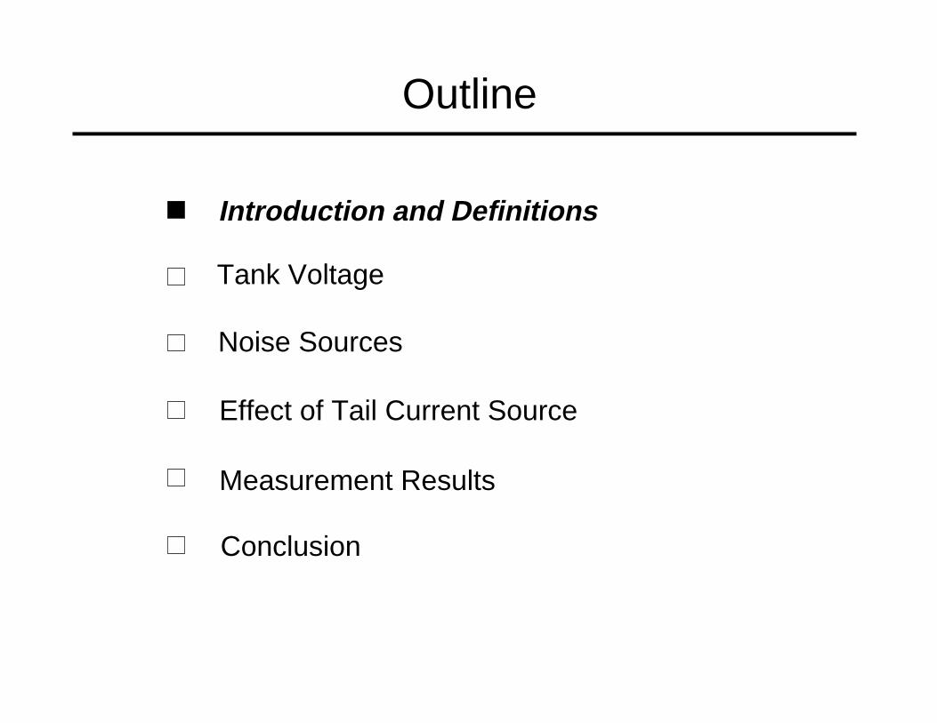
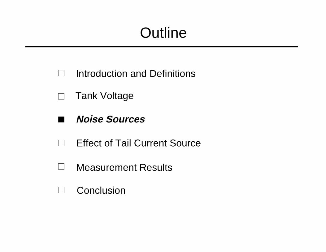
Outline
Introduction and Definitions
Tank Voltage
Measurement Results
Conclusion
Noise Sources
Effect of Tail Current Source

C Li(t)δ t τ–( )
t
i(t)
t
Vout
t
Vout
Oscillators Are Time-Variant Systems
τ
Impulse injected at the peak of amplitude.
∆V
∆V
Even for an ideal LC oscillator, the phase response is Time Variant.
Impulse injected at zero crossing.τ
τ

Once Introduced, phase error persists indefinitely.
Non-linearity quenches amplitude changes over time.
θ
∆θ
V
dVdt--------
LimitCycle
a
b
∆V
Active Device
C Lδ t τ–( )
t
i(t)
τ
G -G(A)
Amplitude Restoring Mechanism
i(t)

Phase Impulse Response
φ t( )hφ t τ,( )
0 t
i(t)
τ 0 τ
hφ t τ,( )Γ ωoτ( )
qmax-------------------u t τ–( )=
t
i t( )
The unit impulse response is:
Γ x( ) is a dimensionless function periodic in 2π, describing how much
phase change results from applying an impulse at time: t Tx
2π------=
The phase impulse response of an arbitrary oscillator is a time varying step.
t
t
t
t
V out t( ) V out t( )
Γ ω0t( ) Γ ω0t( )
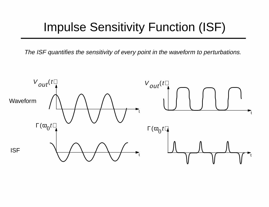
Impulse Sensitivity Function (ISF)
The ISF quantifies the sensitivity of every point in the waveform to perturbations.
Waveform
ISF

φ t( ) hφ t τ,( )i τ( )dτ∞–
∞
∫1
qmax---------------- Γ ω0τ( )i τ( )dτ
∞–
t
∫= =
φ t( )i t( )hφ t τ,( )
Γ ω0τ( )
qmax-------------------u t τ–( )=
Superposition Integral:
Phase Response to an Arbitrary Source
Γ ω0t( )
∞–t
∫ ω0t φ t( )+[ ]cosi t( )
qmax----------------
φ t( )ψ t( ) V t( )
IdealIntegration
PhaseModulation
Equivalent representation:

i t( ) φ t( ) V t( )hφ t τ,( ) ω0t φ t( )+[ ]cos
LTV system Nonlinear system
Phase Noise Due to White Noise
i n2
∆f---------
L ∆ω{ }Γrms
2
qmax2
----------------in
2 ∆f⁄
2∆ω2-------------------⋅=
For a white input noise current with spectral density of
the phase noise sideband power below the carrier at an offset of ∆ω is:
Γrms is the rms value of the ISF.
,
where

c0c1 c2 c3
2ω0ω0 3ω0ω
Sφ ω( )
i n2
∆f------- ω( )
1f--- Noise
Sv ω( )
2ω0ω0 3ω0ω
ω
PM∆ω
∆ω ∆ω ∆ω
∆ω
Noise Contributions from nωo
φ t( ) 1qmax------------- c0 i τ( )dτ
∞–
t
∫ cn i τ( ) nωτ( )cos dτ∞–
t
∫n 1=
∞
∑+=
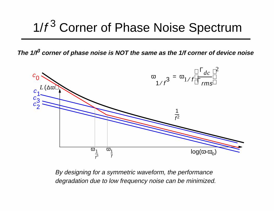
1/f 3 Corner of Phase Noise Spectrum
ω1 f
3⁄ω1 f⁄
ΓdcΓrms--------------
2
=
The 1/f3 corner of phase noise is NOT the same as the 1/f corner of device noise
log(ω-ωo)
L ∆ω( )
1f 2-----
c0
c1
c2
c3
ω1f---
ω 1
f 3----
By designing for a symmetric waveform, the performancedegradation due to low frequency noise can be minimized.

L/2
C
Vdd
A Symmetric LC Oscillator
Uses the same current twice for high transconductance.
WN/L
WP/L
WN/L
WP/L
Adjust ratiosto fine tune
[Also appears in: J.Craninckx, et al, Proceedings of CICC 97.]
symmetry
L/2

Outline
Introduction and Definitions
Tank Voltage
Measurement Results
Conclusion
Noise Sources
Effect of Tail Current Source

L
C
VDD
Itail
Itail
Itail
Tank Voltage Amplitude
Itail
-Itail
t
i(t)
Assuming fast switching of the
differential pair, the current can
be approximated as:
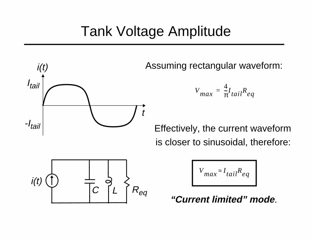
ReqLCi(t)
Itail
-Itail
t
i(t)
Tank Voltage Amplitude
Assuming rectangular waveform:
Vmax4π--- I tailReq=
Effectively, the current waveform
is closer to sinusoidal, therefore:
Vmax I tailReq≈
“Current limited” mode .

2 4 6 8 10 12 14 16 18 20
Tail current (mA)
0.5
1.0
1.5
2.0
2.5
3.0
3.5
Tan
k vo
ltage
sw
ing
(vol
t)
Vdd=1.5V
Vdd=2.5V
Vdd=3.0V
Modes of Amplitude Limiting
Voltage Limited
Current Limited
Complementary cross-coupled LC oscillator
Outline
Introduction and Definitions
Tank Voltage
Measurement Results
Conclusion
Noise Sources
Effect of Tail Current Source

i p12 i p2
2
in12
in22
i tail2
L
C
VDD
bias
vrs2 rs
Major Noise Sources
Different noise sources affect
phase noise differently.
in2
∆f------ 4kTγµCox
WL----- VGS VT–( )=
Valid in both long and short
channel regimes.
Inductor Noise:
vn2
∆f------ 4kT rs=
C
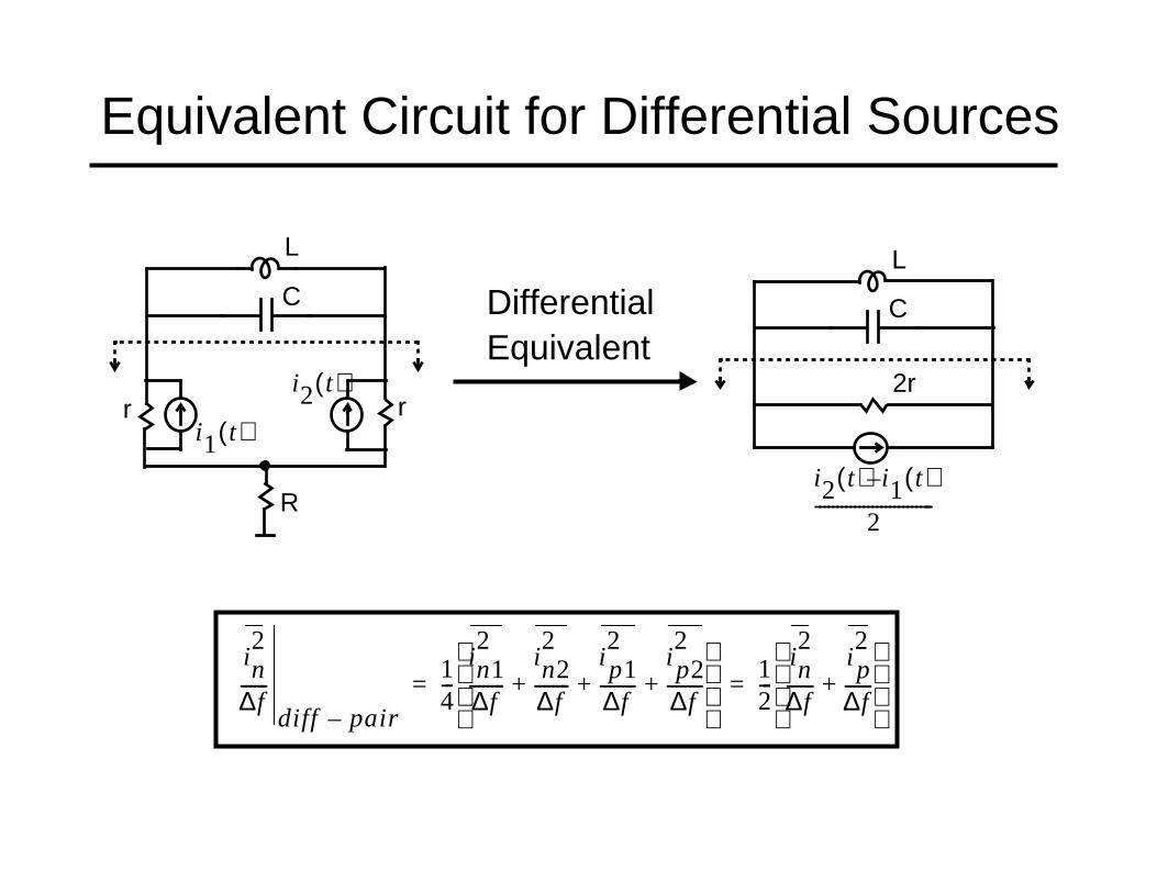
L
i1 t( )
i2 t( )r r
R
C
L
i2 t( ) i1– t( )
2---------------------------
2r
Equivalent Circuit for Differential Sources
DifferentialEquivalent
in2
∆f------
diff pair–
14---
in12
∆f--------
in22
∆f--------
i p12
∆f--------
i p22
∆f--------+ + +
12---
in2
∆f------
i p2
∆f------+
= =

Outline
Introduction and Definitions
Tank Voltage
Measurement Results
Conclusion
Noise Sources
Effect of Tail Current Source
0.5
1.0
1.5
2.0
2.5
Nod
e V
olta
ge (
V)
0.0 1.0 2.0 3.0 4.0 5.0 6.0x (radians)
-1.5
-1.0
-0.5
0.0
0.5
1.0
1.5
ISF
V+V-
Vtail
NMOS ISF
PMOS ISF
Tail ISF
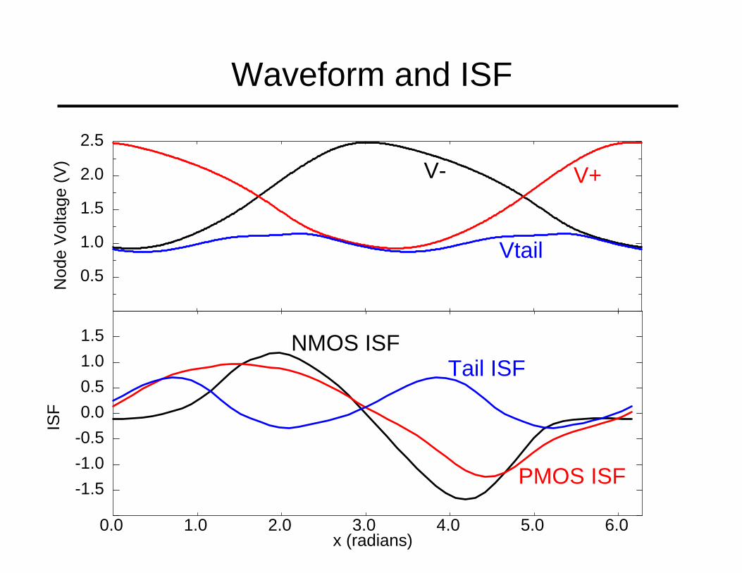
Waveform and ISF
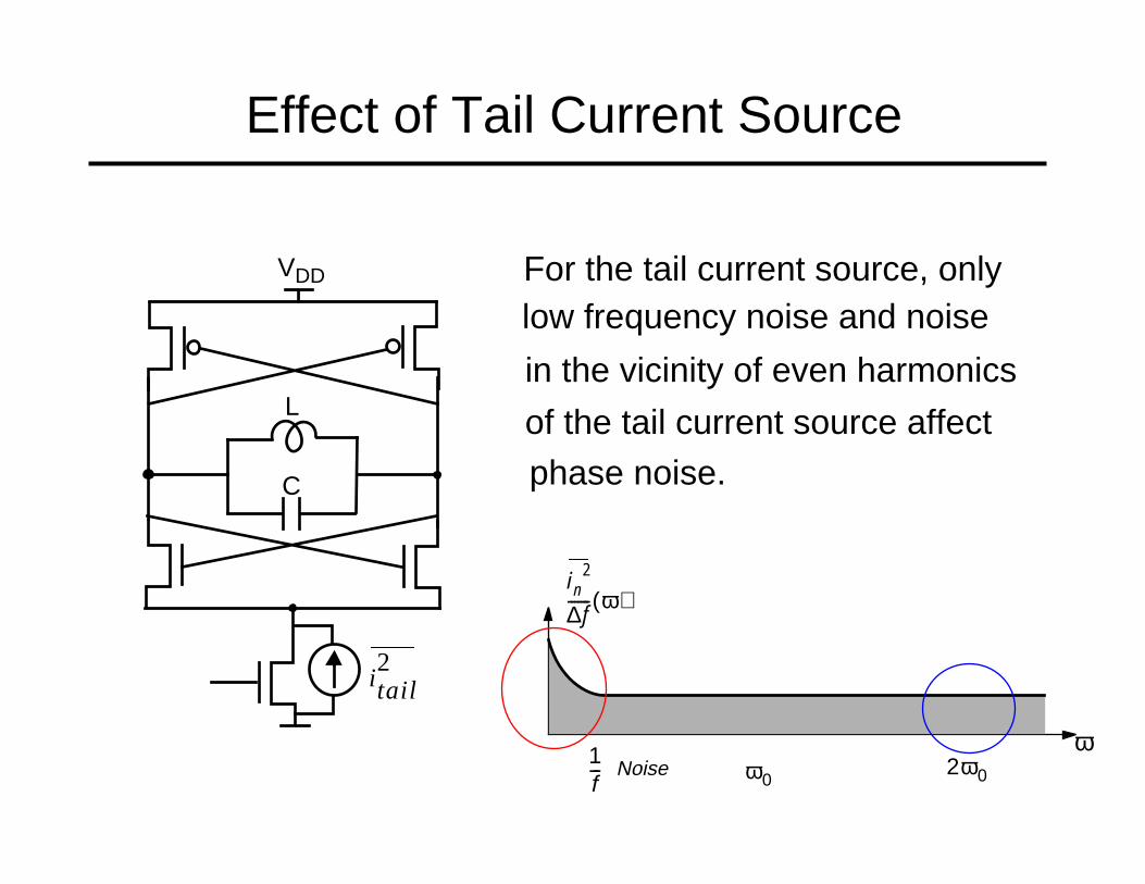
Effect of Tail Current Source
L
C
VDD
2ω0ω0
ω
i n2
∆f------- ω( )
1f--- Noise
i tail2
For the tail current source, only
in the vicinity of even harmonics
of the tail current source affect
phase noise.
low frequency noise and noise

Outline
Introduction and Definitions
Tank Voltage
Measurement Results
Conclusion
Noise Sources
Effect of Tail Current Source
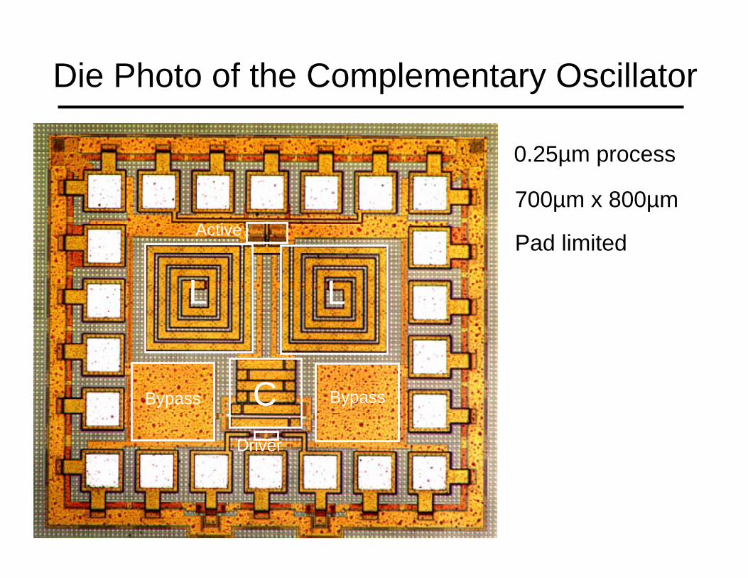
Die Photo of the Complementary Oscillator
700µm x 800µm
L L
C
Active
Bypass Bypass
Driver
Pad limited
0.25µm process
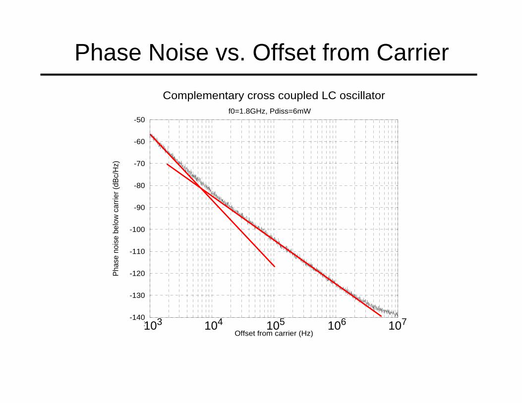
103
104
105
106
107
Offset from carrier (Hz)
-140
-130
-120
-110
-100
-90
-80
-70
-60
-50P
hase
noi
se b
elow
car
rier
(dB
c/H
z)
Complementary cross coupled LC oscillatorf0=1.8GHz, Pdiss=6mWatt
106 107103 104 105
Phase Noise vs. Offset from Carrier
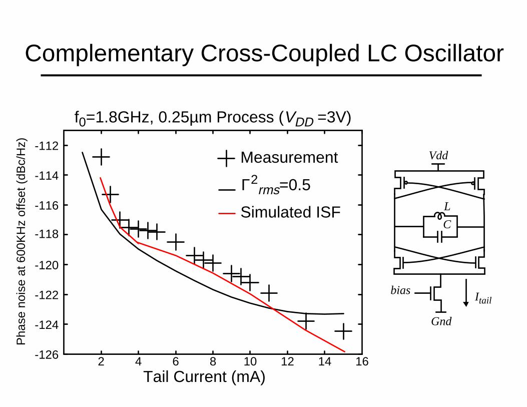
2 4 6 8 10 12 14 16Tail Current (mA)
-126
-124
-122
-120
-118
-116
-114
-112
Pha
se n
oise
at 6
00K
Hz
offs
et (
dBc/
Hz)
f0=1.8GHz, 0.25µm Process (VDD =3V)
Measurement
Complementary Cross-Coupled LC Oscillator
C
L
Vdd
bias
Gnd
Itail
Γ2rms=0.5
Simulated ISF
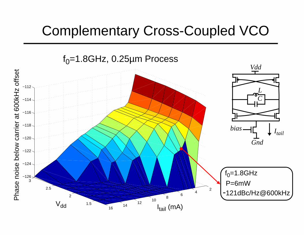
Complementary Cross-Coupled VCO
1.5
2
2.5
3
24
68
1012
1416
x 10−3
−126
−124
−122
−120
−118
−116
−114
−112
f0=1.8GHz, 0.25µm Process
Pha
se n
oise
bel
ow c
arrie
r at
600
kHz
offs
et
Vdd Itail (mA)
-121dBc/Hz@600kHz
f0=1.8GHz
P=6mW
CL
Vdd
bias
Gnd
Itail
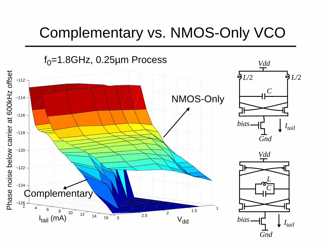
Complementary vs. NMOS-Only VCO
Vdd
C
bias
Gnd
L/2 L/2
Itail
CL
Vdd
bias
Gnd
Itail
11.5
22.5
3
2 4 6 8 10 12 14 16
x 10−3
−126
−124
−122
−120
−118
−116
−114
−112
f0=1.8GHz, 0.25µm Process
VddItail (mA)
Pha
se n
oise
bel
ow c
arrie
r at
600
kHz
offs
et
NMOS-Only
Complementary
Conclusion
● The effect of tail current source on the amplitude is discussed.
● Major noise sources are identified.
● Phase noise of differential MOS oscillators is analyzed.
● The effect of tail current source noise is shown.
● Good agreement between theory and measurements is observed.