opto-mechanical design of the cosmic hot interstellar ...srk/minisat/interestingprojects... ·...
TRANSCRIPT
Opto-mechanical Design of the Cosmic Hot Interstellar Plasma Spectrometer (CHIPS)
M. Sholla, W. Donakowskia, M.M. Sirka, T. Claussb, M. Lamptona, J. Edelsteina, M. Hurwitza
aSpace Sciences Laboratory, University of California, Berkeley CA, USA
bPhysikalisches Insitut, University of Tubingen, Tubingen, Germany
ABSTRACT CHIPS is a NASA UNEX mission designed for diffuse background spectroscopy in the EUV bandpass from 90-260Å. The spectrometer is optimized for peak resolution near 170Å, in order to study diffuse emissions from cooling million degree plasma. Details of local bubble thermal pressure, spatial distribution, and ionization history are the goals of CHIPS observations. We discuss the opto-mechanical design adopted to meet the throughput, signal to noise, and spectral resolution requirements within the mass, volume, and budgetary constraints of a UNEX Delta-II secondary payload. Mechanical tolerance requirements for the six spectrometer channels are discussed, along with details of the lightweight mounting scheme for CHIPS diffraction gratings, front cover slit mechanisms and thermal design. Finally, visible light and vacuum alignment techniques are discussed, as well as with methods employed to minimize stray light. Keywords: Shape memory alloy, semi-kinematic, optical mounting, flexures, diffuse EUV astronomy
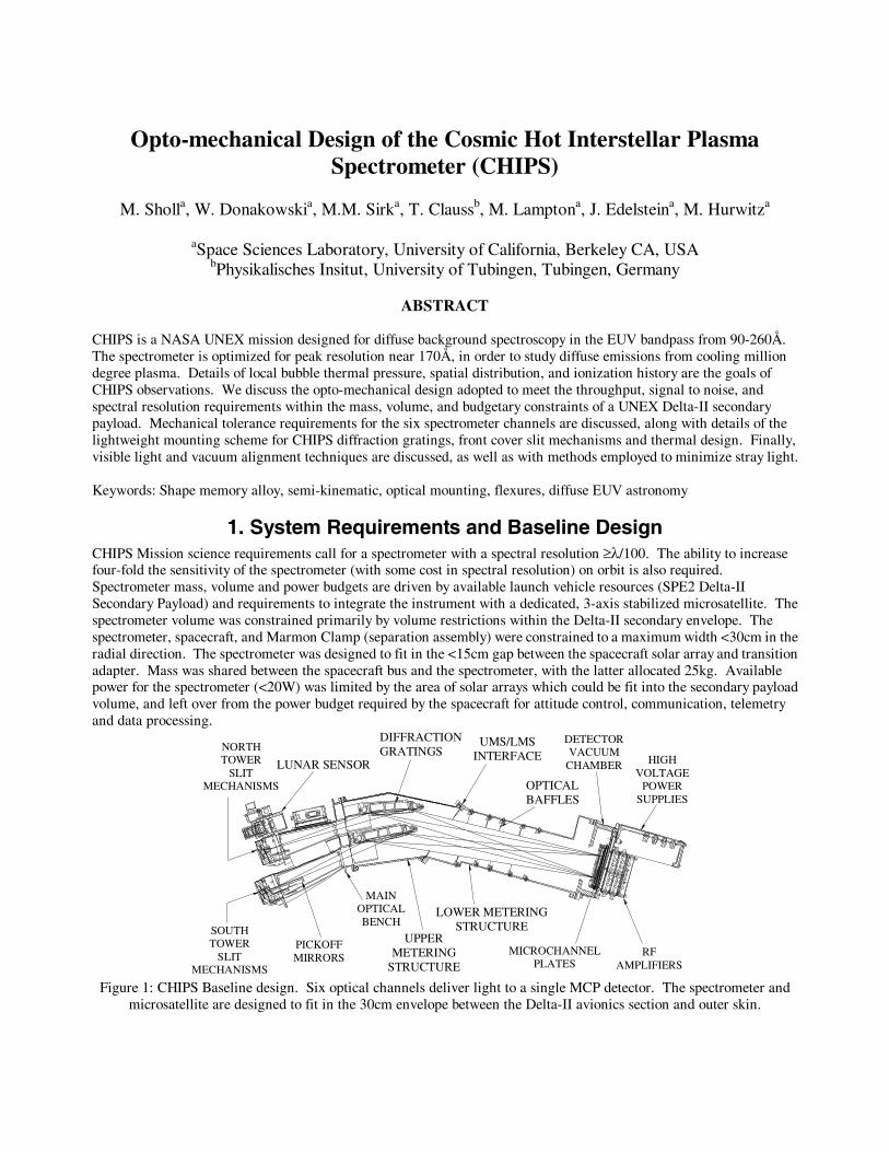
1. System Requirements and Baseline Design CHIPS Mission science requirements call for a spectrometer with a spectral resolution ≥λ/100. The ability to increase four-fold the sensitivity of the spectrometer (with some cost in spectral resolution) on orbit is also required. Spectrometer mass, volume and power budgets are driven by available launch vehicle resources (SPE2 Delta-II Secondary Payload) and requirements to integrate the instrument with a dedicated, 3-axis stabilized microsatellite. The spectrometer volume was constrained primarily by volume restrictions within the Delta-II secondary envelope. The spectrometer, spacecraft, and Marmon Clamp (separation assembly) were constrained to a maximum width <30cm in the radial direction. The spectrometer was designed to fit in the <15cm gap between the spacecraft solar array and transition adapter. Mass was shared between the spacecraft bus and the spectrometer, with the latter allocated 25kg. Available power for the spectrometer (<20W) was limited by the area of solar arrays which could be fit into the secondary payload volume, and left over from the power budget required by the spacecraft for attitude control, communication, telemetry and data processing.
LUNAR SENSOR
UPPERMETERING
STRUCTURE
LOWER METERINGSTRUCTURE
UMS/LMSINTERFACE
OPTICALBAFFLES
DIFFRACTIONGRATINGS
MICROCHANNELPLATES
MAINOPTICALBENCH
PICKOFFMIRRORS
NORTHTOWER
SLITMECHANISMS
SOUTHTOWER
SLITMECHANISMS
DETECTORVACUUM
CHAMBER HIGHVOLTAGE
POWERSUPPLIES
RFAMPLIFIERS
Figure 1: CHIPS Baseline design. Six optical channels deliver light to a single MCP detector. The spectrometer and
microsatellite are designed to fit in the 30cm envelope between the Delta-II avionics section and outer skin.
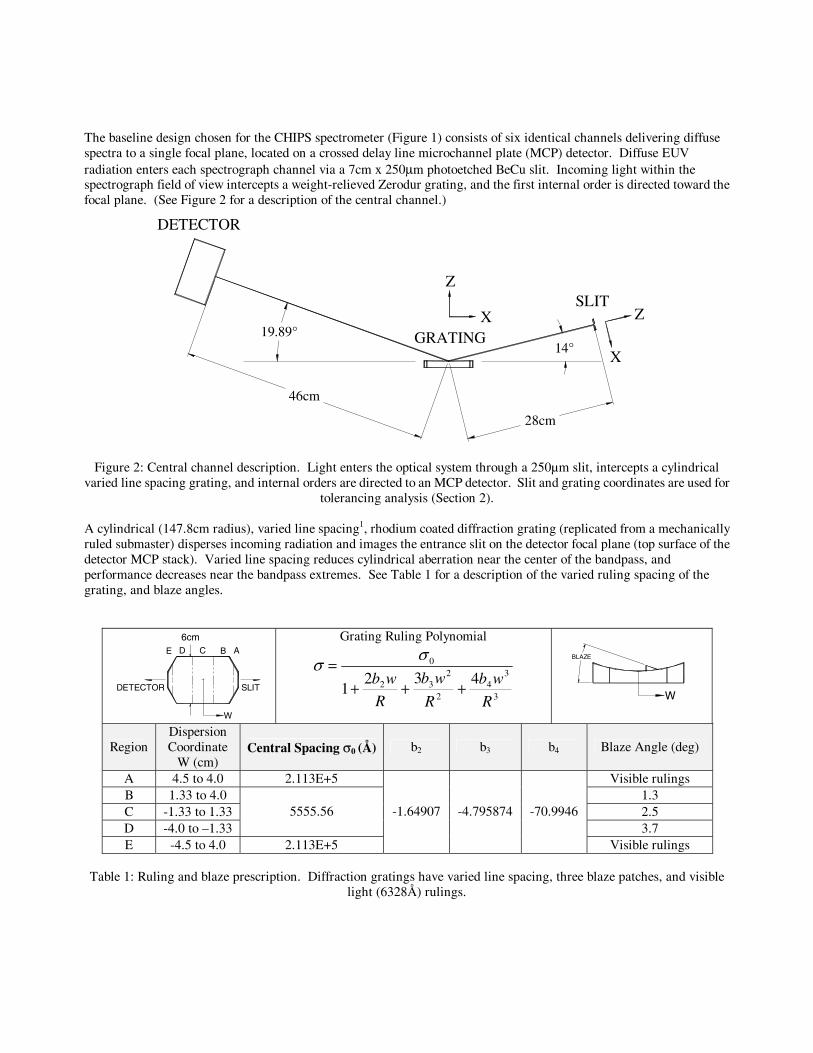
The baseline design chosen for the CHIPS spectrometer (Figure 1) consists of six identical channels delivering diffuse spectra to a single focal plane, located on a crossed delay line microchannel plate (MCP) detector. Diffuse EUV radiation enters each spectrograph channel via a 7cm x 250µm photoetched BeCu slit. Incoming light within the spectrograph field of view intercepts a weight-relieved Zerodur grating, and the first internal order is directed toward the focal plane. (See Figure 2 for a description of the central channel.)
14°
46cm
28cm
19.89°
DETECTOR
GRATING
SLIT
X
ZX
Z
Figure 2: Central channel description. Light enters the optical system through a 250µm slit, intercepts a cylindrical
varied line spacing grating, and internal orders are directed to an MCP detector. Slit and grating coordinates are used for tolerancing analysis (Section 2).
A cylindrical (147.8cm radius), varied line spacing1, rhodium coated diffraction grating (replicated from a mechanically ruled submaster) disperses incoming radiation and images the entrance slit on the detector focal plane (top surface of the detector MCP stack). Varied line spacing reduces cylindrical aberration near the center of the bandpass, and performance decreases near the bandpass extremes. See Table 1 for a description of the varied ruling spacing of the grating, and blaze angles.
ABCDE
W
SLITDETECTOR
6cm
Grating Ruling Polynomial
3
34
2
232
0
4321
R
wb
R
wb
R
wb +++=
σσ
BLAZE
W
Region Dispersion Coordinate
W (cm) Central Spacing σ0 (Å) b2 b3 b4 Blaze Angle (deg)
A 4.5 to 4.0 2.113E+5 Visible rulings B 1.33 to 4.0 1.3 C -1.33 to 1.33 2.5 D -4.0 to –1.33
5555.56 3.7
E -4.5 to 4.0 2.113E+5
-1.64907 -4.795874 -70.9946
Visible rulings Table 1: Ruling and blaze prescription. Diffraction gratings have varied line spacing, three blaze patches, and visible
light (6328Å) rulings.
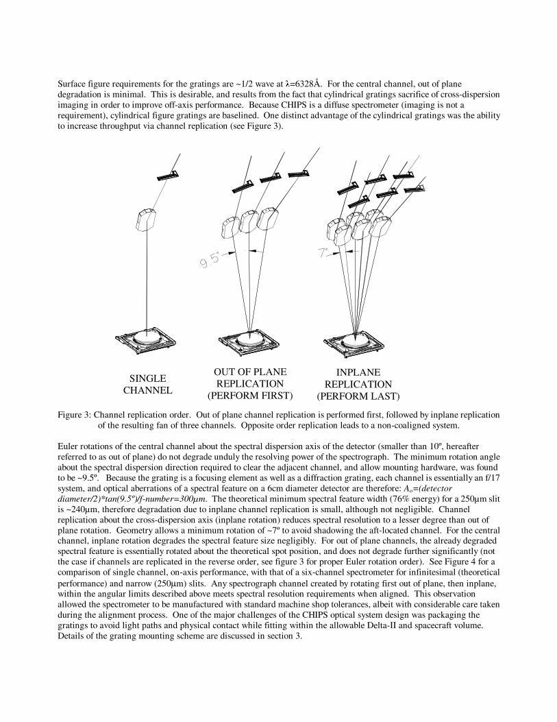
Surface figure requirements for the gratings are ~1/2 wave at λ=6328Å. For the central channel, out of plane degradation is minimal. This is desirable, and results from the fact that cylindrical gratings sacrifice of cross-dispersion imaging in order to improve off-axis performance. Because CHIPS is a diffuse spectrometer (imaging is not a requirement), cylindrical figure gratings are baselined. One distinct advantage of the cylindrical gratings was the ability to increase throughput via channel replication (see Figure 3).
SINGLECHANNEL
OUT OF PLANEREPLICATION
(PERFORM FIRST)
INPLANEREPLICATION
(PERFORM LAST)
Figure 3: Channel replication order. Out of plane channel replication is performed first, followed by inplane replication of the resulting fan of three channels. Opposite order replication leads to a non-coaligned system.
Euler rotations of the central channel about the spectral dispersion axis of the detector (smaller than 10º, hereafter referred to as out of plane) do not degrade unduly the resolving power of the spectrograph. The minimum rotation angle about the spectral dispersion direction required to clear the adjacent channel, and allow mounting hardware, was found to be ~9.5º. Because the grating is a focusing element as well as a diffraction grating, each channel is essentially an f/17 system, and optical aberrations of a spectral feature on a 6cm diameter detector are therefore: Ao=(detector diameter/2)*tan(9.5º)/f-number=300µm. The theoretical minimum spectral feature width (76% energy) for a 250µm slit is ~240µm, therefore degradation due to inplane channel replication is small, although not negligible. Channel replication about the cross-dispersion axis (inplane rotation) reduces spectral resolution to a lesser degree than out of plane rotation. Geometry allows a minimum rotation of ~7º to avoid shadowing the aft-located channel. For the central channel, inplane rotation degrades the spectral feature size negligibly. For out of plane channels, the already degraded spectral feature is essentially rotated about the theoretical spot position, and does not degrade further significantly (not the case if channels are replicated in the reverse order, see figure 3 for proper Euler rotation order). See Figure 4 for a comparison of single channel, on-axis performance, with that of a six-channel spectrometer for infinitesimal (theoretical performance) and narrow (250µm) slits. Any spectrograph channel created by rotating first out of plane, then inplane, within the angular limits described above meets spectral resolution requirements when aligned. This observation allowed the spectrometer to be manufactured with standard machine shop tolerances, albeit with considerable care taken during the alignment process. One of the major challenges of the CHIPS optical system design was packaging the gratings to avoid light paths and physical contact while fitting within the allowable Delta-II and spacecraft volume. Details of the grating mounting scheme are discussed in section 3.
50 100 150 200 250
102
103
104
Theoretical Performance (Infinitesimal Slits)
Wavelength, Angstroms
Res
olvi
ng P
ower
λ/d
λ
One Channel SystemSix Channel System
50 100 150 200 2500
20
40
60
80
100
120
140
160
180
200
Narrow (250 µm) Slits
Wavelength, Angstroms
Res
olvi
ng P
ower
λ/d
λ
One Channel SystemSix Channel System
Figure 4: Performance Limits of CHIPS Optical System. Spectral resolution degradations are comparable for the 250µm slits, and 6-channel replication. Both are system resolution compromises employed to increase throughput.
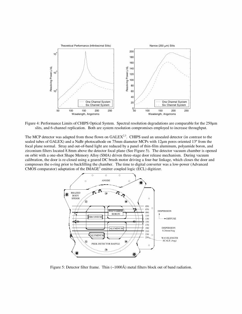
The MCP detector was adapted from those flown on GALEX2,3. CHIPS used an unsealed detector (in contrast to the sealed tubes of GALEX) and a NaBr photocathode on 75mm diameter MCPs with 12µm pores oriented 13º from the focal plane normal. Stray and out-of-band light are reduced by a panel of thin-film aluminum, polyamide boron, and zirconium filters located 8.8mm above the detector focal plane (See Figure 5). The detector vacuum chamber is opened on orbit with a one-shot Shape Memory Alloy (SMA) driven three-stage door release mechanism. During vacuum calibration, the door is re-closed using a geared DC brush motor driving a four-bar linkage, which closes the door and compresses the o-ring prior to backfilling the chamber. The time to digital converter was a low-power (Advanced CMOS comparator) adaptation of the IMAGE3 emitter coupled logic (ECL) digitizer.
150130110090070050
170190210230250
ALUMINUM
ALUMINUM
DIFFUSE
DISPERSION
WAVELENGTHSCALE (Ang)
ZIRCONIUM
POLYAMIDEBORON
PEEK DETECTOR BAFFLE
BRAZEDBODY
SPIDER
ANODE
DISPERSION0.24mm/Ang
Figure 5: Detector filter frame. Thin (~1000Å) metal filters block out of band radiation.
2. Optical Tolerancing and Alignment Tolerance limits for the CHIPS optical system are determined via Monte-Carlo raytracing simulations of numerically aberrated spectrometer incarnations. Slits and gratings are assigned possible ranges of misalignment, and random misalignments are applied by the raytracing code. Both Gaussian random distribution, and maximum (error multiplied by a random sign) misalignments are applied, and effects on spectral resolution (76% energy width of a 170Å spot) quantified. The system is designed for initial adjustment using visible ruling patches on the gratings. The raytracing code simulates resolution improvements, which may be realized via slit post-alignment. Although automated systems exist for single channel optical systems, they are not terribly useful on a system with multiple channels feeding light to a single focal plane. For this reason, a custom raytracing code was developed for CHIPS tolerance analysis. Using the code, roughly 40 sets of error levels were analyzed, each with 10 randomly aberrated incarnations of the spectrometer, and 2000 rays per channel. Tolerance limits for the initial alignment were determined from this study, and are detailed in Table 2. See figure 2 for descriptions of the optical coordinates X, Y and Z, mentioned in Table 2.
Error Magnitude Notes Slit translation X 1mm Shift along narrow dimension, roughly toward solar array Slit translation Y 1mm Spectrometer is insensitive to slit shifts in this direction Slit translation Z 0.5mm Slow optical system (channel) has low sensitivity to focus Grating translation X 0.25mm Translation toward Main Optical Bench (MOB) Grating translation Y 1mm Spectrometer in insensitive to grating shifts in this direction Grating translation Z 0.25mm Piston motion of grating Slit rotation about X 0.5º Mainly defocus Slit rotation about Y 1.0º Negligible effect for small angles (<10º) Slit rotation about Z 1.0º Slit Z rotation may be corrected by slit push Grating rotation about X 0.5º Largely corrected by slit Z rotation Grating rotation about Y 0.1º Most sensitive parameter in entire system (coalignment) Visible/EUV resolution 10µm Limits of visible or EUV alignment Temperature variation 20ºC Expected to be motion of spots due to metering structure gradient
Table 2: Mechanical tolerances. Initial mechanical tolerances requirements are not unduly tight (with the exception of Y
grating rotation). Grating Y rotation is obviously the most sensitive parameter on the instrument. Rotations of the grating about this axis result in a relatively large shift of spectral features in the dispersion direction (roughly 270µm/Arcmin). Initial alignment is achieved by directing light to a pair of visible ruling patches, located on the ends of the gratings. These patches have line spacing defined by the ruling prescription (see Table 1), but spacing larger by a factor of the He-Ne emmision line divided by the spectrometer central wavelength (6328Å/166.38Å). This allows visible light to be diffracted off patches at the ends of the gratings, toward the detector. Diffraction efficiency is quite poor from the visible ruling patches, because tool depth and blaze angles are optimized for EUV rulings (roughly 40 times smaller than the visible rulings). During early alignment, the MCP focal plane is replaced with a ground glass focal plane known as the detector optical surrogate (DOS). This glass is held in place by a machined aluminum holder, which positions the ground glass at the same location as the upper MCP surface. Two CMOS 640x480 cameras image opposite ends of the ground glass screen, and provide highly magnified glimpses of line width at the ends of the He-Ne spectral feature (plate scale=50µm/pixel). Initial alignment of the instrument is achieved using this camera system, and a 6-degree of freedom manipulator mechanism. This mechanism attaches to the grating mount, and the back of the grating under alignment. Front row (North Tower) gratings must be installed and aligned first, because the adjustment mechanism would interfere with any gratings located behind the misaligned grating. All initial alignments are performed in an alignment metering structure substitute which allows access from behind the North Tower gratings (access which would be impossible through the metering structure). A frame grabber is used to store visible images for later analysis. Channels are co-aligned to a thin

wire located on the ground glass screen. Although individual channels are not difficult to align, co-alignment between the six channels proved to be a major challenge. Final alignment is attempted after analysis of EUV data obtained during calibration runs (performed in the SSL Large Vacuum Chamber). For these small (~100µm) motions, a pair ¼in-80tpi micrometer stages is integrated with each slit mechanism, mount fasteners loosened, micrometers moved to correct slit misalignments, and fasteners tightened. The visible ruling patches were found to be significant sources of stray light during EUV calibration. High-order (~25) EUV radiation was found to be directed into the detector, by the visible ruling patches. Because the light is in-band, the thin-film filters do not adequately block stray light from these patches. Light directed toward the patches is blocked by an aluminized Mylar baffle located on the MOB. This baffle is sized by directing rays on a CAD system from the slit extremes, to the edges of the active area on the grating. This baffle is adequate to block light either the near (closest to MOB) patch, or the far (closest to detector) patch. It has the added benefit of blocking the majority of stray light present in the tower end of the MOB. Because the end of the grating nearest the detector is readily accessible, rays diffracted from that patch are blocked by an aluminized Mylar baffle attached directly to the detector-end grating facet. The MOB baffle was chosen to block light heading toward the other visible patch: that closest the MOB. When these baffles are installed, scattered light from the visible rulings are not observed in EUV calibration measurements.
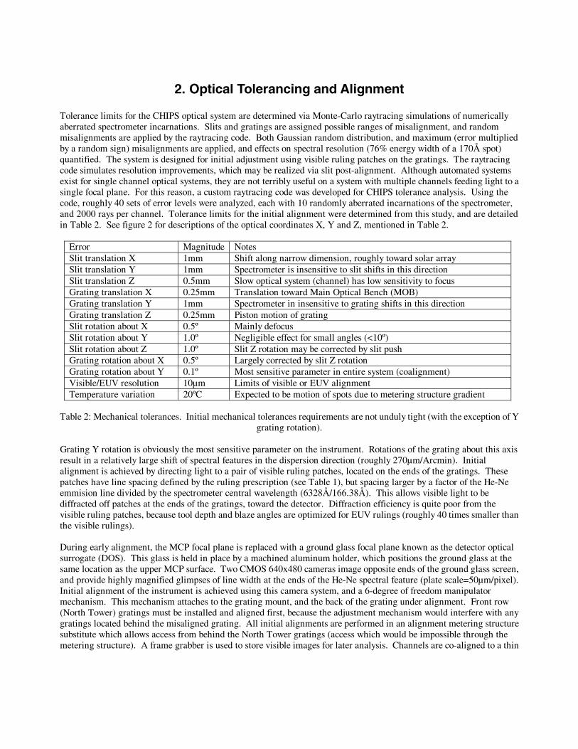
3. Grating Mounts Major drivers for the grating mounts design are mass and volume available for the optics. In order to stay within the cost and schedule constraints of UNEX, traditional fabrication techniques were employed where possible. Additional design guidelines included:
• Lightweight grating substrates (<100gram goal) • No metal on glass contact • No reliance on glue bonds (fasteners and through holes are to be used) • Avoid Invar (use common materials, without need for heat treatment) • Semi-kinematic design principles to be employed • No blocked light on adjacent channels • Design for 52g loads (3-sigma Delta-II secondary payload random level inputs) • Common mount design for all six channels
Because front surfaces of the back row of gratings (and associated light paths) are close to the back surfaces of the front row, and the serious envelope restrictions of the Delta-II SPE2 accommodations, mount hardware growth in the grating normal and anti-normal directions was impossible. Grating mounts may not be located in front of, or behind the gratings. Grating mounts are located in the diverging space between the gratings, near the MOB, and consist of three BeCu flexure blades. The blades are designed to constrain motion of the mount structure in directions radial to the geometric center of the grating5 (thereby allowing a thermal mismatch between the grating and the mount, while maintaining precise alignment) (see Figure 6).
GRATINGHOLDER
BRACKET (Al)
BeCu FLEXURE
WEIGHTRELIEF
RIBSALLOWEDMOTION
CONSTRAINEDMOTION
GRATING
Figure 6: Grating mount design. Semi-kinematic principles are implemented. Flexures constrain motion tangential to the geometric center of the grating (including motion out of the page), while allowing motion toward the grating center.
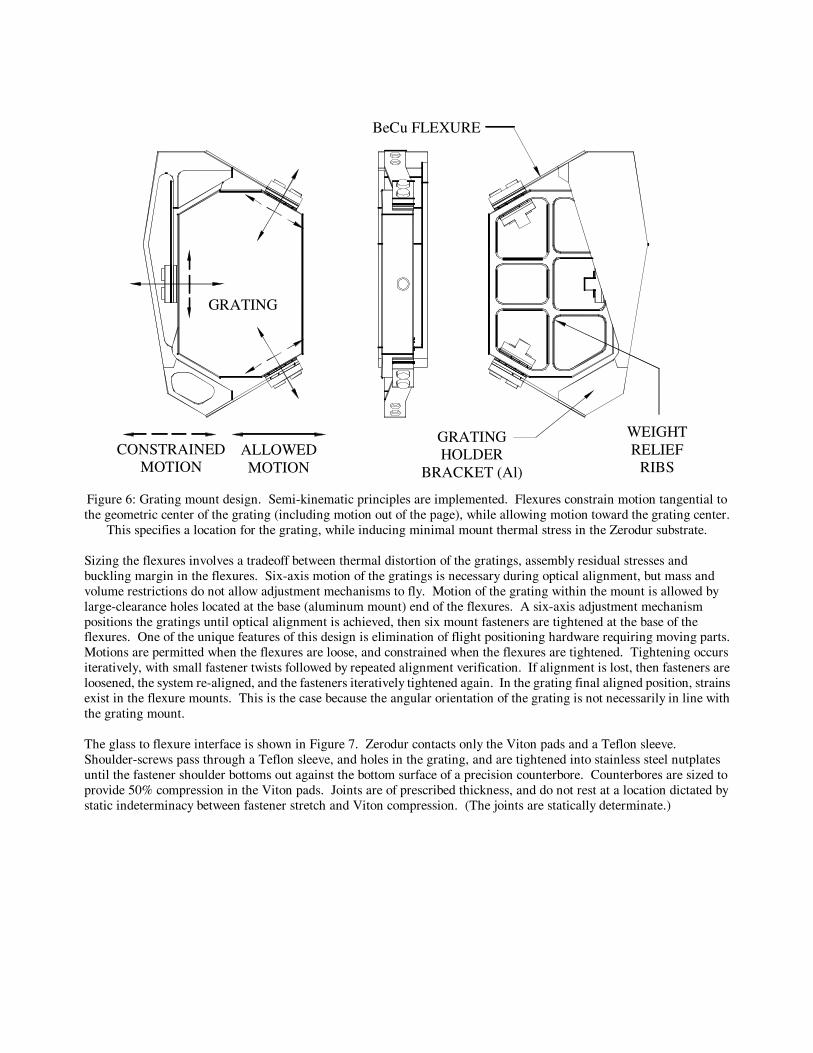
This specifies a location for the grating, while inducing minimal mount thermal stress in the Zerodur substrate. Sizing the flexures involves a tradeoff between thermal distortion of the gratings, assembly residual stresses and buckling margin in the flexures. Six-axis motion of the gratings is necessary during optical alignment, but mass and volume restrictions do not allow adjustment mechanisms to fly. Motion of the grating within the mount is allowed by large-clearance holes located at the base (aluminum mount) end of the flexures. A six-axis adjustment mechanism positions the gratings until optical alignment is achieved, then six mount fasteners are tightened at the base of the flexures. One of the unique features of this design is elimination of flight positioning hardware requiring moving parts. Motions are permitted when the flexures are loose, and constrained when the flexures are tightened. Tightening occurs iteratively, with small fastener twists followed by repeated alignment verification. If alignment is lost, then fasteners are loosened, the system re-aligned, and the fasteners iteratively tightened again. In the grating final aligned position, strains exist in the flexure mounts. This is the case because the angular orientation of the grating is not necessarily in line with the grating mount. The glass to flexure interface is shown in Figure 7. Zerodur contacts only the Viton pads and a Teflon sleeve. Shoulder-screws pass through a Teflon sleeve, and holes in the grating, and are tightened into stainless steel nutplates until the fastener shoulder bottoms out against the bottom surface of a precision counterbore. Counterbores are sized to provide 50% compression in the Viton pads. Joints are of prescribed thickness, and do not rest at a location dictated by static indeterminacy between fastener stretch and Viton compression. (The joints are statically determinate.)
ZERODUR
SS NUTPLATE
TEFLON SLEEVE
BeCu FLEXURE
(50% COMPRESSION)
(50% COMPRESSION)
BONDED JOINTS
(LOCKING)
TRANSITION FIT
WASHERPLATESHOULDER SCREW
OUTER SS PLATE
OUTER VITON PAD
INNER VITON
PH-BR HELICOIL
Figure 7: Details of Zerodur clamp. The glass to flexure joint is sized to compress Viton to 50% of its original thickness
when the shoulder screw shanks bottom out in a precision stainless steel counterbore.
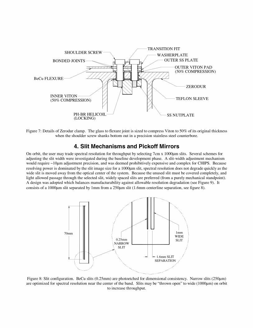
4. Slit Mechanisms and Pickoff Mirrors On orbit, the user may trade spectral resolution for throughput by selecting 7cm x 1000µm slits. Several schemes for adjusting the slit width were investigated during the baseline development phase. A slit-width adjustment mechanism would require ~10µm adjustment precision, and was deemed prohibitively expensive and complex for CHIPS. Because resolving power is dominated by the slit image size for a 1000µm slit, spectral resolution does not degrade quickly as the wide slit is moved away from the optical center of the system. Because the unused slit must be covered completely, and light allowed passage through the selected slit, widely spaced slits are preferred (from a purely mechanical standpoint). A design was adopted which balances manufacturability against allowable resolution degradation (see Figure 9). It consists of a 1000µm slit separated by 1mm from a 250µm slit (1.6mm centerline separation, see figure 8).
1.6mm SLITSEPARATION
0.25mmNARROW
SLIT
1mmWIDESLIT
70mm
Figure 8: Slit configuration. BeCu slits (0.25mm) are photoetched for dimensional consistency. Narrow slits (250µm) are optimized for spectral resolution near the center of the band. Slits may be “thrown open” to wide (1000µm) on orbit
to increase throughput.
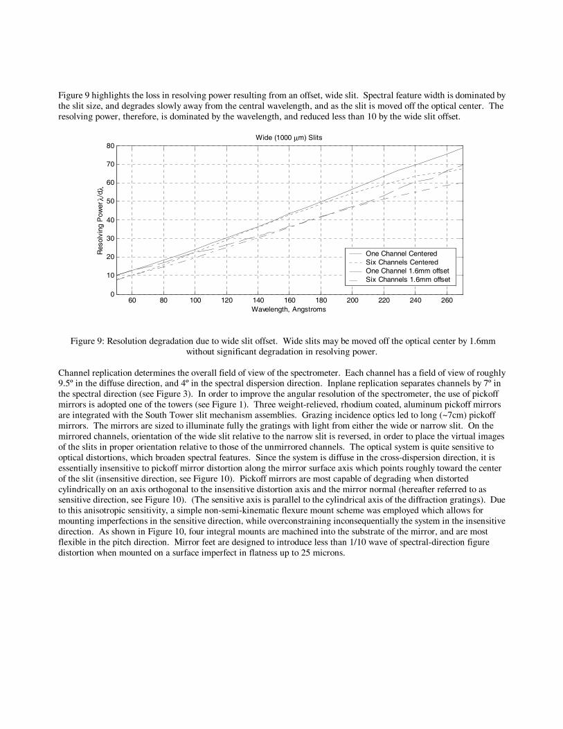
Figure 9 highlights the loss in resolving power resulting from an offset, wide slit. Spectral feature width is dominated by the slit size, and degrades slowly away from the central wavelength, and as the slit is moved off the optical center. The resolving power, therefore, is dominated by the wavelength, and reduced less than 10 by the wide slit offset.
60 80 100 120 140 160 180 200 220 240 2600
10
20
30
40
50
60
70
80Wide (1000 µm) Slits
Wavelength, Angstroms
Res
olvi
ng P
ower
λ/d
λ
One Channel CenteredSix Channels CenteredOne Channel 1.6mm offsetSix Channels 1.6mm offset
Figure 9: Resolution degradation due to wide slit offset. Wide slits may be moved off the optical center by 1.6mm without significant degradation in resolving power.
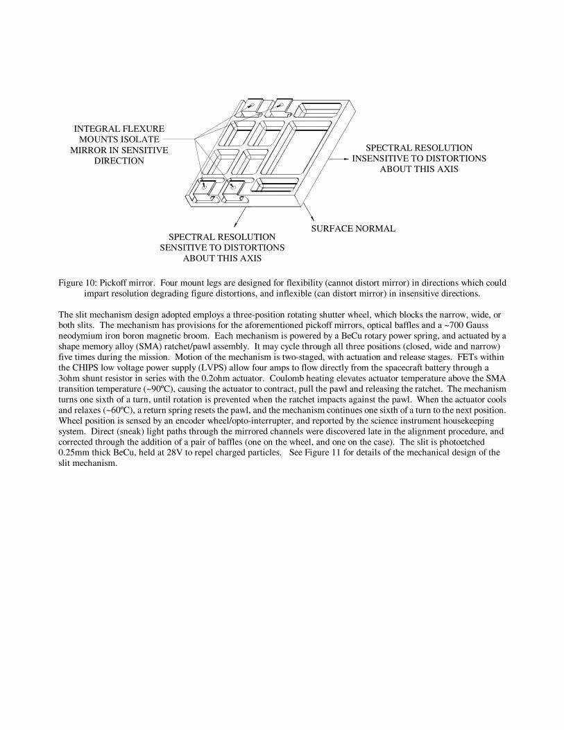
Channel replication determines the overall field of view of the spectrometer. Each channel has a field of view of roughly 9.5º in the diffuse direction, and 4º in the spectral dispersion direction. Inplane replication separates channels by 7º in the spectral direction (see Figure 3). In order to improve the angular resolution of the spectrometer, the use of pickoff mirrors is adopted one of the towers (see Figure 1). Three weight-relieved, rhodium coated, aluminum pickoff mirrors are integrated with the South Tower slit mechanism assemblies. Grazing incidence optics led to long (~7cm) pickoff mirrors. The mirrors are sized to illuminate fully the gratings with light from either the wide or narrow slit. On the mirrored channels, orientation of the wide slit relative to the narrow slit is reversed, in order to place the virtual images of the slits in proper orientation relative to those of the unmirrored channels. The optical system is quite sensitive to optical distortions, which broaden spectral features. Since the system is diffuse in the cross-dispersion direction, it is essentially insensitive to pickoff mirror distortion along the mirror surface axis which points roughly toward the center of the slit (insensitive direction, see Figure 10). Pickoff mirrors are most capable of degrading when distorted cylindrically on an axis orthogonal to the insensitive distortion axis and the mirror normal (hereafter referred to as sensitive direction, see Figure 10). (The sensitive axis is parallel to the cylindrical axis of the diffraction gratings). Due to this anisotropic sensitivity, a simple non-semi-kinematic flexure mount scheme was employed which allows for mounting imperfections in the sensitive direction, while overconstraining inconsequentially the system in the insensitive direction. As shown in Figure 10, four integral mounts are machined into the substrate of the mirror, and are most flexible in the pitch direction. Mirror feet are designed to introduce less than 1/10 wave of spectral-direction figure distortion when mounted on a surface imperfect in flatness up to 25 microns.
SURFACE NORMAL
SPECTRAL RESOLUTIONINSENSITIVE TO DISTORTIONS
ABOUT THIS AXIS
SENSITIVE TO DISTORTIONSABOUT THIS AXIS
SPECTRAL RESOLUTION
INTEGRAL FLEXUREMOUNTS ISOLATE
MIRROR IN SENSITIVEDIRECTION
Figure 10: Pickoff mirror. Four mount legs are designed for flexibility (cannot distort mirror) in directions which could
impart resolution degrading figure distortions, and inflexible (can distort mirror) in insensitive directions.
The slit mechanism design adopted employs a three-position rotating shutter wheel, which blocks the narrow, wide, or both slits. The mechanism has provisions for the aforementioned pickoff mirrors, optical baffles and a ~700 Gauss neodymium iron boron magnetic broom. Each mechanism is powered by a BeCu rotary power spring, and actuated by a shape memory alloy (SMA) ratchet/pawl assembly. It may cycle through all three positions (closed, wide and narrow) five times during the mission. Motion of the mechanism is two-staged, with actuation and release stages. FETs within the CHIPS low voltage power supply (LVPS) allow four amps to flow directly from the spacecraft battery through a 3ohm shunt resistor in series with the 0.2ohm actuator. Coulomb heating elevates actuator temperature above the SMA transition temperature (~90ºC), causing the actuator to contract, pull the pawl and releasing the ratchet. The mechanism turns one sixth of a turn, until rotation is prevented when the ratchet impacts against the pawl. When the actuator cools and relaxes (~60ºC), a return spring resets the pawl, and the mechanism continues one sixth of a turn to the next position. Wheel position is sensed by an encoder wheel/opto-interrupter, and reported by the science instrument housekeeping system. Direct (sneak) light paths through the mirrored channels were discovered late in the alignment procedure, and corrected through the addition of a pair of baffles (one on the wheel, and one on the case). The slit is photoetched 0.25mm thick BeCu, held at 28V to repel charged particles. See Figure 11 for details of the mechanical design of the slit mechanism.

SHOULDER SCREWOPTOWHEEL
BeCu POWER SPRING
RATCHET WHEEL
SLIT WHEEL
OPTOSENSOR
NdFeB MAGNET
PAWL
SLIT
MIRROR MOUNT
MECHANISM CASEBALL BEARING
RETURNSPRING
SMAACTUATOR
BALLBEARING
Figure 11: Slit Mechanism. Slit wheels are powered by BeCu power springs, and initiated by a 2-stage nitinol actuated ratchet/pawl assembly. The wheel has channels, which allow light to pass through either the wide, narrow or neither slit. As in the case of the grating mounts, slit mechanisms are designed with the goal of maximum parts commonality for the various channels. For the six slit mechanisms, all parts are common between the North and South Tower (see Figure 1) with the exception of: Pickoff mirrors, baffles (shown in Figure 12), slits, and slit wheels. Because the relative positions of the slits are reversed between the mirrored, and non-mirrored channels, the slits and slit wheels were required to differ. All six mechanisms progress from closed, to narrow, to wide in the same order. Figure 12 details differences between the mirrored and non-mirrored slit mechanisms, and show the light paths through the wheels in all possible configurations.
SLIT WHEEL
WIDE
BeCu SLIT
PICKOFF
CLOSED
BAFFLE
BAFFLE
NARROW WIDECLOSED NARROW
MIRRORED NONMIRRORED
Figure 12: Mirrored and nonmirrored slit mechanisms. CHIPS is launched with slit mechanisms in the closed position. Slit wheels have three positions: closed, wide and narrow, separated by 120º. On mirrored channels, baffles prevent
direct “sneak” rays from reaching the gratings.
5. Conclusions CHIPS was designed to observe the largely unexplored band between 90 and 260Å. The design overcame a number of challenging packaging, optical mount, operational mode, and cost challenges in order to deliver an observatory capable of collecting the required science data. Shape memory alloy actuators were used throughout the design, and a lightweight, low-profile, BeCu flexure mount scheme was developed. A visible-light alignment scheme was employed, in conjunction with EUV alignment to achieve the desired system coalignment and spectral resolution. Lightweight baffles made from aluminized Mylar allowed quick modifications, late in the calibration phase, in order to mitigate stray light issues. CHIPS is integrated with a dedicated 3-axis stabilized microsatellite, and expected to launch on a Delta-II.
REFERENCES 1. Harada,T; Kita,T; Bowyer,S; Hurwitz,M, “Design of Spherical Varied Line-Space Gratings for a High-Resolution
EUV Spectrometer.” SPIE 1545, pp. 2-10, 1991. 2. O.H.W. Siegmund, P. Jelinsky, S. Jelinsky, J. Stock, J. Hull, D. Doliber, J. Zaninovich, A.S. Tremsin and K.
Kromer, "High resolution cross delay line detectors for the GALEX mission." Proc. SPIE 3765, "EUV, X-Ray, and Gamma-Ray Instrumentation for Astronomy X", Denver, pp.429-440, 1999.
3. Lampton, M., “The Microchannel Image Intensifier.” SCI-AMER, pp.46-55, 1981. 4. Lampton, M., “A Timing Discriminator for Space Flight Applications.” American Institute of Physics Review of
Scientific Instruments Volume 69, Number 8, P 3062-3065, August 1998. 5. Yoder, P., Opto-Mechanical Systems Design, Marcel Dekker, Inc., New York, 1993.
ACKNOWLEDGMENTS
The authors wish to acknowledge the input of Pat Jelinsky (University of California at Berkeley, Space Sciences Laboratory) for early design and raytracing, and numerous discussions on the design of CHIPS. Geoff Gaines (Gaines Systems, Berkeley, CA) provided invaluable assistance to the CHIPS program in EUV calibration. Jeremy McCauley, Ken McKee, Jereb Mirczak, Steven Sulack, Michael Ting and Karl Kromer were involved with design of a number of mechanical subsystems on CHIPS.
This work was supported by the Office of Space Sciences, National Aeronautics and Space Administration, under Grant No. NAG5-5219. Contact: [email protected]; tel. (USA) 510-643-2098; Space Sciences Laboratory, University of California, Berkeley, CA 94720 USA.