optimal design of lcl harmonic filters for three-phase … design of lcl harmonic filters for ... in...
TRANSCRIPT
© 2011 IEEE
Proceedings of the 37th Annual Conference of the IEEE Industrial Electronics Society (IECON 2011), Melbourne, Australia,November 7-10, 2011.
Optimal Design of LCL Harmonic Filters for Three-Phase PFC Rectifiers
J. MühlethalerM. SchweizerR. BlattmannJ. W. KolarA. Ecklebe
This material is posted here with permission of the IEEE. Such permission of the IEEE does not in any way imply IEEE endorsement of any of ETH Zurich‘s products or services. Internal or personal use of this material is permitted. However, permission to reprint/republish this material for advertising or promotional purposes or for creating new collective works for resale or redistribution must be obtained from the IEEE by writing to [email protected]. By choosing to view this document, you agree to all provisions of the copyright laws protecting it.
Optimal Design of LCL Harmonic Filters forThree-Phase PFC Rectifiers
J. Muhlethaler∗, M. Schweizer∗, R. Blattmann∗, J. W. Kolar∗, and A. Ecklebe†∗Power Electronic Systems Laboratory, ETH Zurich, Email: [email protected]
†ABB Switzerland Ltd., Corporate Research, CH-5405 Baden-Dattwil
Abstract—Inductive components such as line filter inductorsor transformers occupy a significant amount of space in today’spower electronic systems, and furthermore, considerable lossesoccur in these components. A main application of filter inductorsare EMI filters, as e.g. employed for the attenuation of switchingfrequency harmonics of PFC rectifier systems. In this paper adesign procedure for the mains side LCL filter of an active three-phase rectifier is introduced. The procedure is based on a genericoptimization approach, which guarantees a low volume and/orlow losses. Different designs are calculated to show the trade-offbetween filter volume and filter losses. The design procedure isverified by experimental measurements.
I. INTRODUCTION
The trend in power electronics research is towards higherefficiency and higher power density of converter systems. Thistrend is driven by cost considerations, e.g. material economies,space limitations, e.g. for automotive applications, and increas-ing efficiency requirements, e.g. for telecom applications. Theincrease of the power density often affects the efficiency, i.e.a trade-off between these two quality indices exists [1].
Inductive components occupy a significant amount of spacein today’s power electronic systems, and furthermore, con-siderable losses occur in these components. Therefore, inorder to increase the power density and/or efficiency of powerelectronic systems, losses in inductive components must bereduced, and/or new cooling concepts need to be investigated.
At the Power Electronic Systems Laboratory at ETH Zuricha project has been initiated with the goal to establish compre-hensive models of inductive power components which can beadapted to various geometric properties, operating conditionsand cooling conditions. These models will form the basis forthe optimization of inductive components employed in keypower electronics applications. The aim of this paper is to usethese previously derived models to design LCL input filtersof a three-phase Power Factor Correction (PFC) rectifier.LCL input filters are an attractive solution to attenuate
switching frequency current harmonics of active voltage sourcerectifiers [2], [3]. In this work a design procedure for LCLfilters based on a generic optimization approach is introducedguaranteeing low volume and/or low losses. Different designsare calculated showing the trade-off between filter volume andfilter losses.
In Section II the three-phase PFC rectifier is introduced, inSection III the applied models of the LCL filter componentsare discussed, and in Section IV the optimization algorithmis described. Simulation and experimental results are given inSections V and VI respectively.
TABLE ISPECIFICATION OF THE THREE-PHASE PFC RECITIFIER
Parameter Variable ValueInput Voltage AC Vmains 230 VMains Frequency fmains 50 HzDC-Voltage VDC 650 VLoad Current IL (nominal) 15.4 ASwitching Frequency fsw 8 kHz
II. THREE-PHASE PFC RECTIFIER WITH INPUT FILTER
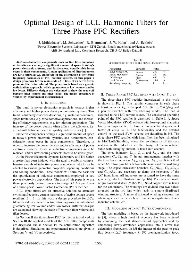
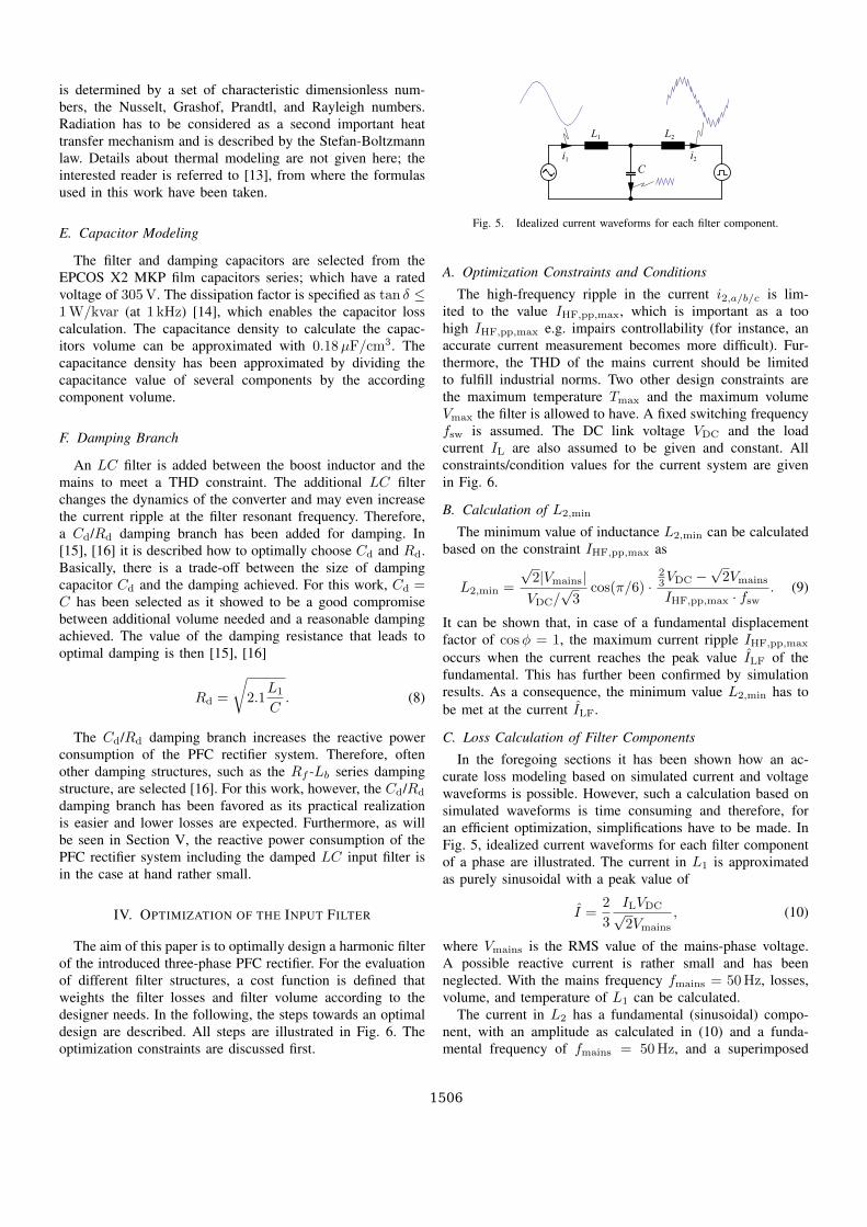
The three-phase PFC rectifier investigated in this workis shown in Fig. 1. The rectifier comprises in each phasea boost inductor L2, a damped LC filter L1/C/Cd/Rd anda pair of switches with free-wheeling diodes. The load isassumed to be a DC current source. The considered operatingpoint of the PFC rectifier is described in Table I. A SpaceVector Modulation (SVM) scheme with loss-optimal clampinghas been implemented to have a fundamental displacementfactor of cosφ = 1. The functionality and the detailedcontrol of the used SVM scheme are described in [4]. Thethree-phase PFC rectifier with input filter has been simulatedin MATLAB/Simulink, where the non-linearity of the corematerial of the inductors, i.e. the change of the inductancevalue with changing current, is taken into account.
The three inductors L1,a, L1,b, and L1,c, and the threecapacitors Ca, Cb, and Cc in star arrangement, together withthe three boost inductors L2,a, L2,b and L2,c, result in a thirdorder LCL low pass filter between the mains and the switchingstage. The capacitor/resistor branches Cd,a/Rd,a, Cd,b/Rd,b,and Cd,c/Rd,c are necessary to damp the resonance of theLC input filter. All inductors are assumed to have the samegeometry, which is illustrated in Fig. 1(b). The cores are madeof grain-oriented steel (M165-35S). Solid copper wire is takenfor the conductors. The windings are divided into two halvesarranged on the two legs which leads to a more distributedwinding structure. A more distributed winding structure hasadvantages such as better heat dissipation capabilities, lowerinductor volume, etc.
III. MODELING OF INPUT FILTER COMPONENTS
The loss modeling is based on the framework introducedin [5], where a high level of accuracy has been achievedby combining the best state-of-the-art approaches and byembedding newly-developed approaches into a novel losscalculation framework. In [5] the impact of the peak-to-peakflux density ∆B, frequency f , DC premagnetization HDC,
978-1-61284-972-0/11/$26.00 ©2011 IEEE 1503
VDC IL
L1,a
L1,b
L1,c
L2,a
L2,b
L2,c
Cb
i1,a i2,a
w
w
do
N/2N/2
ww
d
a
B
A
Winding
t
(a) (b)
h
Cd,b
Rd,b
Ca
Cd,a
Cc
Cd,c
Rd,cRd,a
IL
a
b
c
Vmains
Fig. 1. (a) Three-phase PFC rectifier with LCL input filter. (b) Cross-sections of inductors employed in the input filter.
temperature T , core shape, minor and major BH-loops, fluxwaveform, and material on the core loss calculation has beenconsidered. In order to calculate the winding losses, formulasfor round conductors and litz wires, each considering skin-and proximity effects and also considering the influence of anair-gap fringing field have been included. In the following, adiscussion about the implemented models for the employedinductors (cf. Fig. 1(b)) is given.
A. Calculation of the InductanceThe inductance of an inductive component with N winding
turns and a total magnetic reluctance Rm,tot is calculated as
L =N2
Rm,tot. (1)
Accordingly, the reluctance of each section of the flux pathhas to be derived first in order to calculate Rm,tot. The totalreluctance for a general inductor is calculated as a functionof the core reluctances and air gap reluctances. The core andair gap reluctances can be determined applying the methodsdescribed in [6]. The reluctances of the core depend on therelative permeability µr which is defined by the (nonlinear)BH-relation of the core material, hence the reluctance isdescribed as a function of the flux. Therefore, as the fluxdepends on the core reluctance and the reluctance dependson the flux, the system can only be solved iteratively by usinga numerical method. In the case at hand, the problem has beensolved by applying the Newton approach.
The reluctance model of the inductance of Fig. 1(b) consistsof one voltage source (representing the two separated wind-ings), one air gap reluctance (representing the two air gaps)and one core reluctance. The fact that the flux density in coreparts very close to the air gap is (slightly) reduced as the fluxlines already left the core has been neglected.
B. Core LossesThe applied core loss approach is described in [5] in
detail and can be seen as a hybrid of the improved-improvedGeneralized Steinmetz Equation i2GSE [7] and a loss map
approach: a loss map is experimentally determined and theinterpolation and extrapolation for operating points in betweenthe measured values is then made with the i2GSE.
The flux density waveform for which the losses have tobe calculated is e.g. simulated in a circuit simulator, wherethe magnetic part is modeled as a reluctance model. Thissimulated waveform is then divided into its fundamental fluxwaveform and into piecewise linear flux waveform segments.The loss energy is then derived for the fundamental and allpiecewise linear segments, summed-up and divided by thefundamental period length in order to determine the averagecore loss. The DC flux level of each piecewise linear fluxsegment is considered, as this influences the core losses [8].Furthermore, the relaxation term of the i2GSE is evaluatedfor each transition from one piecewise linear flux segment toanother.
Another aspect to be considered in the core loss calculationis the effect of the core shape/size. By introducing a reluc-tance model of the core, the flux density can be calculated.Subsequently, for each core section with (approximately)homogenous flux density, the losses can be determined. Inthe case at hand, the core has been divided into four straightcore sections and four corner sections. The core losses of thesections are then summed-up to obtain the total core losses.
C. Winding Losses
The second source of losses in inductive components are theohmic losses in the windings. The resistance of a conductorincreases with increasing frequency due to eddy currents. Self-induced eddy currents inside a conductor lead to the skineffect. Eddy currents due to an external alternating magneticfield, e.g. the air gap fringing field or the magnetic field fromother conductors, lead to the proximity effect.
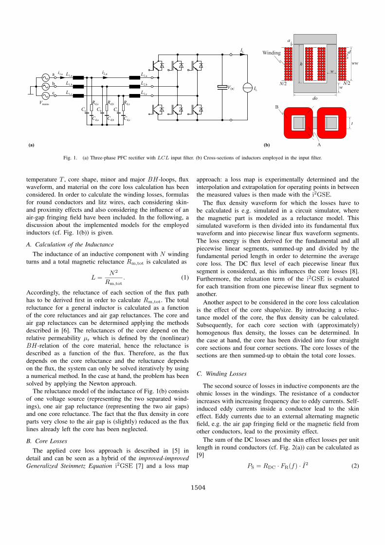
The sum of the DC losses and the skin effect losses per unitlength in round conductors (cf. Fig. 2(a)) can be calculated as[9]
PS = RDC · FR(f) · I2 (2)
1504
zx
y
Jz
d
Jz
d
He
(a) (b)
Fig. 2. Cross-section of the round conductor considered with a current inz-direction. The conductor is infinitely large in z-direction.
and1
FR(f) =ξ
4√
2
(ber0(ξ)bei1(ξ)− ber0(ξ)ber1(ξ)
ber1(ξ)2 + bei1(ξ)2
− bei0(ξ)ber1(ξ) + bei0(ξ)bei1(ξ)
ber1(ξ)2 + bei1(ξ)2
),
(3)
with δ = 1√πµ0σf
, ξ = d√2δ, RDC = 4
σπd2 ; δ is commonlynamed the skin depth, f is the frequency, d is the conductordiameter, and σ is the electric conductivity of the conductormaterial.
The proximity effect losses in round conductors (cf. Fig.2(b)) per unit length can be calculated as [9]
PP = RDC ·GR(f) · H2e (4)
and
GR(f) =− ξπ2d2
2√
2
(ber2(ξ)ber1(ξ) + ber2(ξ)bei1(ξ)
ber0(ξ)2 + bei0(ξ)2
+bei2(ξ)bei1(ξ)− bei2(ξ)ber1(ξ)
ber0(ξ)2 + bei0(ξ)2
).
(5)
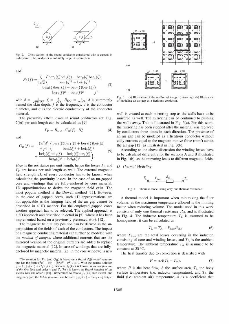
RDC is the resistance per unit length, hence the losses PS andPP are losses per unit length as well. The external magneticfield strength He of every conductor has to be known whencalculating the proximity losses. In the case of an un-gappedcore and windings that are fully-enclosed by core material,1D approximations to derive the magnetic field exist. Themost popular method is the Dowell method [11]. However,in the case of gapped cores, such 1D approximations arenot applicable as the fringing field of the air gap cannot bedescribed in a 1D manner. For the employed gapped coresanother approach has to be selected. The applied approach isa 2D approach and described in detail in [5], where it has beenimplemented based on a previously presented work [12].
The magnetic field at any position can be derived as the su-perposition of the fields of each of the conductors. The impactof a magnetic conducting material can further be modeled withthe method of images, where additional currents that are themirrored version of the original currents are added to replacethe magnetic material [12]. In case of windings that are fully-enclosed by magnetic material (i.e. in the core window), a new
1The solution for FR (and GR) is based on a Bessel differential equationthat has the form x2y′′+xy′+(k2x2−v2)y = 0. With the general solutiony = C1Jv(kx) + C2Yv(kx), whereas Jv(kx) is known as Bessel functionof the first kind and order v and Yv(kx) is known as Bessel function of thesecond kind and order v [10]. Furthermore, to resolve Jv(kx) into its real- andimaginary part, the Kelvin functions can be used: Jv(j
32 x) = bervx+j beivx.
µ → ∞
→
(a)
(b)
µ → ∞ µ → ∞
→
Fig. 3. (a) Illustration of the method of images (mirroring). (b) Illustrationof modeling an air gap as a fictitious conductor.
wall is created at each mirroring step as the walls have to bemirrored as well. The mirroring can be continued to pushingthe walls away. This is illustrated in Fig. 3(a). For this work,the mirroring has been stopped after the material was replacedby conductors three times in each direction. The presence ofan air gap can be modeled as a fictitious conductor withouteddy currents equal to the magneto-motive force (mmf) acrossthe air gap [12] as illustrated in Fig. 3(b).
According to the above discussion the winding losses haveto be calculated differently for the sections A and B illustratedin Fig. 1(b), as the mirroring leads to different magnetic fields.
D. Thermal Modeling
PlossTL TARth
Fig. 4. Thermal model using only one thermal resistance.
A thermal model is important when minimizing the filtervolume, as the maximum temperature allowed is the limitingfactor when reducing volume. The model used in this workconsists of only one thermal resistance Rth and is illustratedin Fig. 4. The inductor temperature TL is assumed to behomogenous; it can be calculated as
TL = TA + PlossRth, (6)
where Ploss are the total losses occurring in the inductor,consisting of core and winding losses, and TA is the ambienttemperature. The ambient temperature TA is assumed to beconstant at 25 ◦C.
The heat transfer due to convection is described with
P = αA(TL − TA), (7)
where P is the heat flow, A the surface area, TL the bodysurface temperature (i.e. inductor temperature), and TA thefluid (i.e. ambient air) temperature. α is a coefficient that
1505
is determined by a set of characteristic dimensionless num-bers, the Nusselt, Grashof, Prandtl, and Rayleigh numbers.Radiation has to be considered as a second important heattransfer mechanism and is described by the Stefan-Boltzmannlaw. Details about thermal modeling are not given here; theinterested reader is referred to [13], from where the formulasused in this work have been taken.
E. Capacitor Modeling
The filter and damping capacitors are selected from theEPCOS X2 MKP film capacitors series; which have a ratedvoltage of 305 V. The dissipation factor is specified as tan δ ≤1 W/kvar (at 1 kHz) [14], which enables the capacitor losscalculation. The capacitance density to calculate the capac-itors volume can be approximated with 0.18µF/cm3. Thecapacitance density has been approximated by dividing thecapacitance value of several components by the accordingcomponent volume.
F. Damping Branch
An LC filter is added between the boost inductor and themains to meet a THD constraint. The additional LC filterchanges the dynamics of the converter and may even increasethe current ripple at the filter resonant frequency. Therefore,a Cd/Rd damping branch has been added for damping. In[15], [16] it is described how to optimally choose Cd and Rd.Basically, there is a trade-off between the size of dampingcapacitor Cd and the damping achieved. For this work, Cd =C has been selected as it showed to be a good compromisebetween additional volume needed and a reasonable dampingachieved. The value of the damping resistance that leads tooptimal damping is then [15], [16]
Rd =
√2.1
L1
C. (8)
The Cd/Rd damping branch increases the reactive powerconsumption of the PFC rectifier system. Therefore, oftenother damping structures, such as the Rf -Lb series dampingstructure, are selected [16]. For this work, however, the Cd/Rd
damping branch has been favored as its practical realizationis easier and lower losses are expected. Furthermore, as willbe seen in Section V, the reactive power consumption of thePFC rectifier system including the damped LC input filter isin the case at hand rather small.
IV. OPTIMIZATION OF THE INPUT FILTER
The aim of this paper is to optimally design a harmonic filterof the introduced three-phase PFC rectifier. For the evaluationof different filter structures, a cost function is defined thatweights the filter losses and filter volume according to thedesigner needs. In the following, the steps towards an optimaldesign are described. All steps are illustrated in Fig. 6. Theoptimization constraints are discussed first.
L1 L2
Ci1 i2
Fig. 5. Idealized current waveforms for each filter component.
A. Optimization Constraints and Conditions
The high-frequency ripple in the current i2,a/b/c is lim-ited to the value IHF,pp,max, which is important as a toohigh IHF,pp,max e.g. impairs controllability (for instance, anaccurate current measurement becomes more difficult). Fur-thermore, the THD of the mains current should be limitedto fulfill industrial norms. Two other design constraints arethe maximum temperature Tmax and the maximum volumeVmax the filter is allowed to have. A fixed switching frequencyfsw is assumed. The DC link voltage VDC and the loadcurrent IL are also assumed to be given and constant. Allconstraints/condition values for the current system are givenin Fig. 6.
B. Calculation of L2,min
The minimum value of inductance L2,min can be calculatedbased on the constraint IHF,pp,max as
L2,min =
√2|Vmains|VDC/
√3
cos(π/6) ·23VDC −
√2Vmains
IHF,pp,max · fsw. (9)
It can be shown that, in case of a fundamental displacementfactor of cosφ = 1, the maximum current ripple IHF,pp,max
occurs when the current reaches the peak value ILF of thefundamental. This has further been confirmed by simulationresults. As a consequence, the minimum value L2,min has tobe met at the current ILF.
C. Loss Calculation of Filter Components
In the foregoing sections it has been shown how an ac-curate loss modeling based on simulated current and voltagewaveforms is possible. However, such a calculation based onsimulated waveforms is time consuming and therefore, foran efficient optimization, simplifications have to be made. InFig. 5, idealized current waveforms for each filter componentof a phase are illustrated. The current in L1 is approximatedas purely sinusoidal with a peak value of
I =2
3
ILVDC√2Vmains
, (10)
where Vmains is the RMS value of the mains-phase voltage.A possible reactive current is rather small and has beenneglected. With the mains frequency fmains = 50 Hz, losses,volume, and temperature of L1 can be calculated.
The current in L2 has a fundamental (sinusoidal) compo-nent, with an amplitude as calculated in (10) and a funda-mental frequency of fmains = 50 Hz, and a superimposed
1506
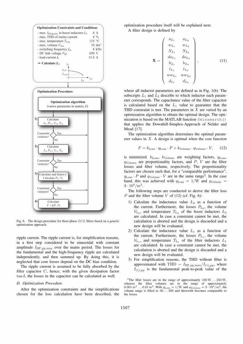
Optimization Constraints and Conditions- max. IHF,pp,max in boost inductors L2- max. THD of mains current- max. temperature Tmax- max. volume Vmax- switching frequency fsw- DC link voltage VDC- load current IL
44
12510
865015.4
A%°Cdm3
kHzVA
Optimization Procedure
Calculate L2
(varies parameter in matrix X)Optimization algorithm
L2,N
ILF
L2,min
L2
iLF
Calculate L2, PL2, VL2, TL2
Constraint violation?
Constraint violation?
Constraint violation?
1)
No
Calculate and Select CCalculate PC, VC
CalculateF = f(P, V)
2)
3)
4)
Calculate L1, PL1, VL1, TL1
Yes
No
Yes
No
Yes
Fig. 6. The design procedure for three-phase LCL filters based on a genericoptimization approach.
ripple current. The ripple current is, for simplification reasons,in a first step considered to be sinusoidal with constantamplitude IHF,pp,max over the mains period. The losses forthe fundamental and the high-frequency ripple are calculatedindependently, and then summed up. By doing this, it isneglected that core losses depend on the DC bias condition.
The ripple current is assumed to be fully absorbed by thefilter capacitor C, hence, with the given dissipation factortan δ, the losses in the capacitor can be calculated as well.
D. Optimization ProcedureAfter the optimization constraints and the simplifications
chosen for the loss calculation have been described, the
optimization procedure itself will be explained next.A filter design is defined by
X =
aL1aL2
wL1wL2
NL1 NL2
doL1 doL2
hL1hL2
tL1tL2
wwL1wwL2
dL1 dL2
, (11)
where all inductor parameters are defined as in Fig. 1(b). Thesubscripts L1 and L2 describe to which inductor each param-eter corresponds. The capacitance value of the filter capacitoris calculated based on the L1 value to guarantee that theTHD constraint is met. The parameters in X are varied by anoptimization algorithm to obtain the optimal design. The opti-mization is based on the MATLAB function fminsearch()that applies the Downhill-Simplex-Approach of Nelder andMead [17].
The optimization algorithm determines the optimal param-eter values in X . A design is optimal when the cost function
F = kLoss · qLoss · P + kVolume · qVolume · V, (12)
is minimized. kLoss, kVolume are weighting factors, qLoss,qVolume are proportionality factors, and P , V are the filterlosses and filter volume, respectively. The proportionalityfactors are chosen such that, for a ”comparable performance”,qLoss · P and qVolume · V are in the same range2. In the casehand, this was achieved with qLoss = 1/W and qVolume =3 · 104/m3.
The following steps are conducted to derive the filter lossP and the filter volume V of (12) (cf. Fig. 6):
1) Calculate the inductance value L2 as a function ofthe current. Furthermore, the losses PL2
, the volumeVL2
, and temperature TL2of the boost inductors L2
are calculated. In case a constraint cannot be met, thecalculation is aborted and the design is discarded and anew design will be evaluated.
2) Calculate the inductance value L1 as a function ofthe current. Furthermore, the losses PL1
, the volumeVL1
, and temperature TL1of the filter inductors L1
are calculated. In case a constraint cannot be met, thecalculation is aborted and the design is discarded and anew design will be evaluated.
3) For simplification reasons, the THD without filter isapproximated with THD = IHF,pp,max/I(1),pp, whereI(1),pp is the fundamental peak-to-peak value of the
2The filter losses are in the range of approximately 100W . . . 250W,whereas the filter volumes are in the range of approximately0.001m3 . . . 0.01m3. With qLoss = 1/W and qVolume = 3 · 104/m3, thevolume range is lifted to 30 . . . 300 and therewith becomes comparable tothe losses.
1507
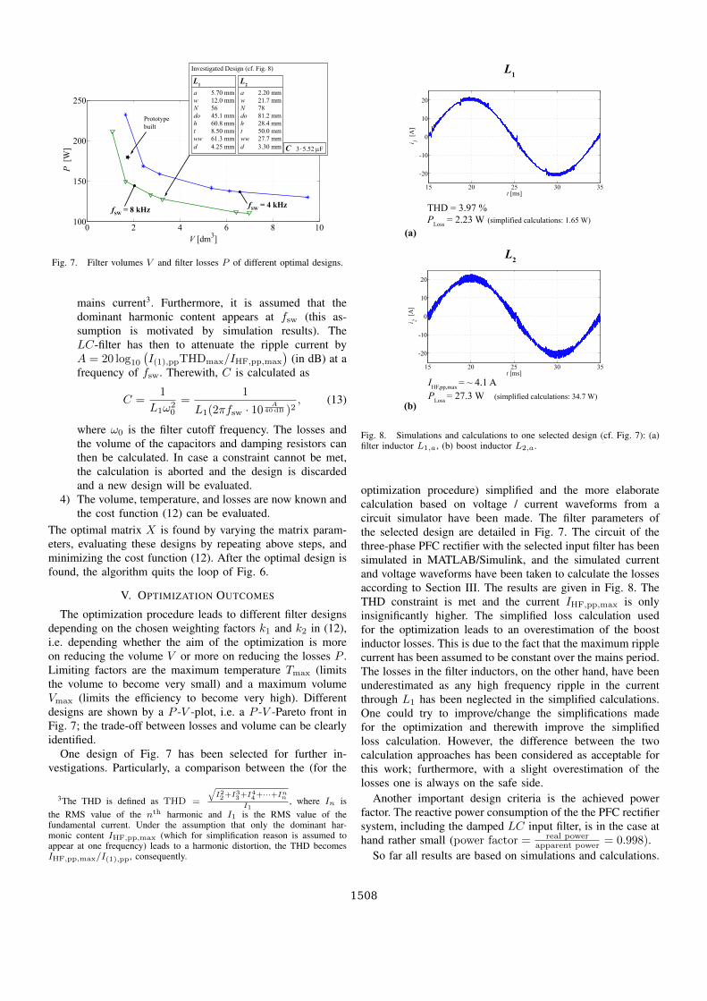
0 2 4 6 8 10100
150
200
250
P [
W]
V [dm3]
Prototype built
L1
awNdohtwwd
5.70 mm12.0 mm5645.1 mm60.8 mm8.50 mm61.3 mm4.25 mm
L2
awNdohtwwd
2.20 mm21.7 mm7881.2 mm28.4 mm50.0 mm27.7 mm3.30 mm C 3 5.52 µF
fSW = 8 kHz fSW = 4 kHz
Investigated Design (cf. Fig. 8)
Fig. 7. Filter volumes V and filter losses P of different optimal designs.
mains current3. Furthermore, it is assumed that thedominant harmonic content appears at fsw (this as-sumption is motivated by simulation results). TheLC-filter has then to attenuate the ripple current byA = 20 log10
(I(1),ppTHDmax/IHF,pp,max
)(in dB) at a
frequency of fsw. Therewith, C is calculated as
C =1
L1ω20
=1
L1(2πfsw · 10A
40 dB )2, (13)
where ω0 is the filter cutoff frequency. The losses andthe volume of the capacitors and damping resistors canthen be calculated. In case a constraint cannot be met,the calculation is aborted and the design is discardedand a new design will be evaluated.
4) The volume, temperature, and losses are now known andthe cost function (12) can be evaluated.
The optimal matrix X is found by varying the matrix param-eters, evaluating these designs by repeating above steps, andminimizing the cost function (12). After the optimal design isfound, the algorithm quits the loop of Fig. 6.
V. OPTIMIZATION OUTCOMES
The optimization procedure leads to different filter designsdepending on the chosen weighting factors k1 and k2 in (12),i.e. depending whether the aim of the optimization is moreon reducing the volume V or more on reducing the losses P .Limiting factors are the maximum temperature Tmax (limitsthe volume to become very small) and a maximum volumeVmax (limits the efficiency to become very high). Differentdesigns are shown by a P -V -plot, i.e. a P -V -Pareto front inFig. 7; the trade-off between losses and volume can be clearlyidentified.
One design of Fig. 7 has been selected for further in-vestigations. Particularly, a comparison between the (for the
3The THD is defined as THD =
√I22+I33+I44+···+Inn
I1, where In is
the RMS value of the nth harmonic and I1 is the RMS value of thefundamental current. Under the assumption that only the dominant har-monic content IHF,pp,max (which for simplification reason is assumed toappear at one frequency) leads to a harmonic distortion, the THD becomesIHF,pp,max/I(1),pp, consequently.
THD = 3.97 %PLoss = 2.23 W (simplified calculations: 1.65 W)
IHF,pp,max = ~ 4.1 APLoss = 27.3 W (simplified calculations: 34.7 W)
L1
(a)
(b)
15 20 25 30 35
-20
-10
0
10
20
i 1 [A
]
t [ms]
15 20 25 30 35
-20
-10
0
10
20
i 2 [A
]
t [ms]
L2
Fig. 8. Simulations and calculations to one selected design (cf. Fig. 7): (a)filter inductor L1,a, (b) boost inductor L2,a.
optimization procedure) simplified and the more elaboratecalculation based on voltage / current waveforms from acircuit simulator have been made. The filter parameters ofthe selected design are detailed in Fig. 7. The circuit of thethree-phase PFC rectifier with the selected input filter has beensimulated in MATLAB/Simulink, and the simulated currentand voltage waveforms have been taken to calculate the lossesaccording to Section III. The results are given in Fig. 8. TheTHD constraint is met and the current IHF,pp,max is onlyinsignificantly higher. The simplified loss calculation usedfor the optimization leads to an overestimation of the boostinductor losses. This is due to the fact that the maximum ripplecurrent has been assumed to be constant over the mains period.The losses in the filter inductors, on the other hand, have beenunderestimated as any high frequency ripple in the currentthrough L1 has been neglected in the simplified calculations.One could try to improve/change the simplifications madefor the optimization and therewith improve the simplifiedloss calculation. However, the difference between the twocalculation approaches has been considered as acceptable forthis work; furthermore, with a slight overestimation of thelosses one is always on the safe side.
Another important design criteria is the achieved powerfactor. The reactive power consumption of the the PFC rectifiersystem, including the damped LC input filter, is in the case athand rather small (power factor = real power
apparent power = 0.998).So far all results are based on simulations and calculations.
1508
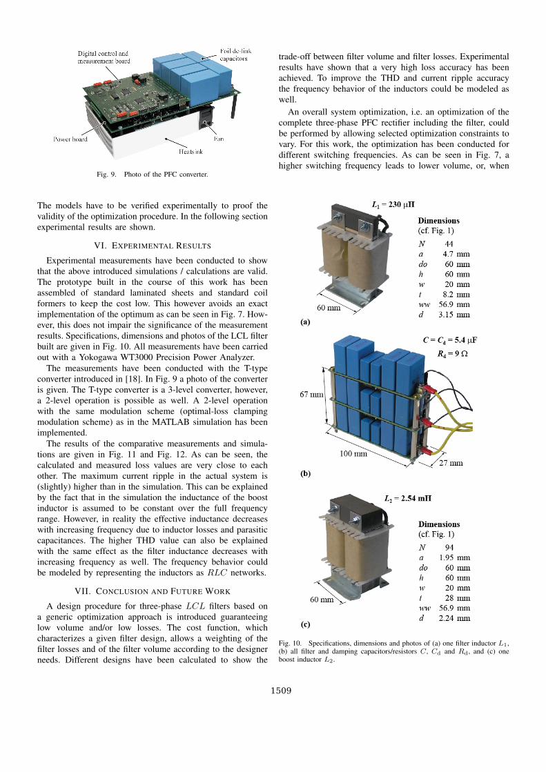
Fig. 9. Photo of the PFC converter.
The models have to be verified experimentally to proof thevalidity of the optimization procedure. In the following sectionexperimental results are shown.
VI. EXPERIMENTAL RESULTS
Experimental measurements have been conducted to showthat the above introduced simulations / calculations are valid.The prototype built in the course of this work has beenassembled of standard laminated sheets and standard coilformers to keep the cost low. This however avoids an exactimplementation of the optimum as can be seen in Fig. 7. How-ever, this does not impair the significance of the measurementresults. Specifications, dimensions and photos of the LCL filterbuilt are given in Fig. 10. All measurements have been carriedout with a Yokogawa WT3000 Precision Power Analyzer.
The measurements have been conducted with the T-typeconverter introduced in [18]. In Fig. 9 a photo of the converteris given. The T-type converter is a 3-level converter, however,a 2-level operation is possible as well. A 2-level operationwith the same modulation scheme (optimal-loss clampingmodulation scheme) as in the MATLAB simulation has beenimplemented.
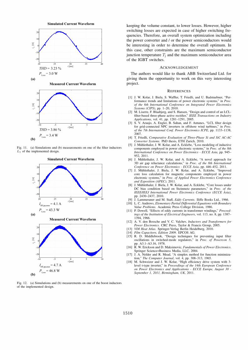
The results of the comparative measurements and simula-tions are given in Fig. 11 and Fig. 12. As can be seen, thecalculated and measured loss values are very close to eachother. The maximum current ripple in the actual system is(slightly) higher than in the simulation. This can be explainedby the fact that in the simulation the inductance of the boostinductor is assumed to be constant over the full frequencyrange. However, in reality the effective inductance decreaseswith increasing frequency due to inductor losses and parasiticcapacitances. The higher THD value can also be explainedwith the same effect as the filter inductance decreases withincreasing frequency as well. The frequency behavior couldbe modeled by representing the inductors as RLC networks.
VII. CONCLUSION AND FUTURE WORK
A design procedure for three-phase LCL filters based ona generic optimization approach is introduced guaranteeinglow volume and/or low losses. The cost function, whichcharacterizes a given filter design, allows a weighting of thefilter losses and of the filter volume according to the designerneeds. Different designs have been calculated to show the
trade-off between filter volume and filter losses. Experimentalresults have shown that a very high loss accuracy has beenachieved. To improve the THD and current ripple accuracythe frequency behavior of the inductors could be modeled aswell.
An overall system optimization, i.e. an optimization of thecomplete three-phase PFC rectifier including the filter, couldbe performed by allowing selected optimization constraints tovary. For this work, the optimization has been conducted fordifferent switching frequencies. As can be seen in Fig. 7, ahigher switching frequency leads to lower volume, or, when
Fig. 10. Specifications, dimensions and photos of (a) one filter inductor L1,(b) all filter and damping capacitors/resistors C, Cd and Rd, and (c) oneboost inductor L2.
1509
-10 -5 0 5
-20
-10
0
10
20
i 1 [A
]
t [ms]
20 25 30 35 40
-20
-10
0
10
20 i 1
[A]
t [ms]
PLoss = 3.0 W
PLoss = 3.4 W
Simulated Current Waveform
(a)
(b)
Measured Current Waveform
THD = 3.23 %
THD = 3.86 %
Fig. 11. (a) Simulations and (b) measurements on one of the filter inductorsL1 of the implemented design.
-10 -5 0 5 10
-20
-10
0
10
20
i 2 [A
]
t [ms]
20 25 30 35 40
-20
-10
0
10
20
i 2 [A
]
t [ms]
PLoss = 43.3 W
PLoss = 46.8 W
Simulated Current Waveform
(a)
(b)
Measured Current Waveform
IHF,pp,max = 4.1 A
IHF,pp,max = 4.7 A
Fig. 12. (a) Simulations and (b) measurements on one of the boost inductorsof the implemented design.
keeping the volume constant, to lower losses. However, higherswitching losses are expected in case of higher switching fre-quencies. Therefore, an overall system optimization includingthe power converter and / or the power semiconductors wouldbe interesting in order to determine the overall optimum. Inthis case, other constraints are the maximum semiconductorjunction temperature Tj and the maximum semiconductor areaof the IGBT switches.
ACKNOWLEDGEMENT
The authors would like to thank ABB Switzerland Ltd. forgiving them the opportunity to work on this very interestingproject.
REFERENCES
[1] J. W. Kolar, J. Biela, S. Waffler, T. Friedli, and U. Badstuebner, “Per-formance trends and limitations of power electronic systems,” in Proc.of the 6th International Conference on Integrated Power ElectronicsSystems (CIPS), pp. 1–20, 2010.
[2] M. Liserre, F. Blaabjerg, and S. Hansen, “Design and control of an LCL-filter-based three-phase active rectifier,” IEEE Transactions on IndustryApplications, vol. 41, pp. 1281–1291, 2005.
[3] S. V. Araujo, A. Engler, B. Sahan, and F. Antunes, “LCL filter designfor grid-connected NPC inverters in offshore wind turbines,” in Proc.of the 7th Internatonal Conf. Power Electronics ICPE, pp. 1133–1138,2007.
[4] T. Friedli, Comparative Evaluation of Three-Phase Si and SiC AC-ACConverter Systems. PhD thesis, ETH Zurich, 2010.
[5] J. Muhlethaler, J. W. Kolar, and A. Ecklebe, “Loss modeling of inductivecomponents employed in power electronic systems,” in Proc. of the 8thInternational Conference on Power Electronics - ECCE Asia, pp. 945–952, 2011.
[6] J. Muhlethaler, J. W. Kolar, and A. Ecklebe, “A novel approach for3D air gap reluctance calculations,” in Proc. of the 8th InternationalConference on Power Electronics - ECCE Asia, pp. 446–452, 2011.
[7] J. Muhlethaler, J. Biela, J. W. Kolar, and A. Ecklebe, “Improvedcore loss calculation for magnetic components employed in powerelectronic systems,” in Proc. of Applied Power Electronics Conferenceand Exposition (APEC), 2011.
[8] J. Muhlethaler, J. Biela, J. W. Kolar, and A. Ecklebe, “Core losses underDC bias condition based on Steinmetz parameters,” in Proc. of theIEEE/IEEJ International Power Electronics Conference (ECCE Asia),pp. 2430–2437, 2010.
[9] J. Lammeraner and M. Stafl, Eddy Currents. Iliffe Books Ltd., 1966.[10] L. C. Andrews, Elementary Partial Differential Equations with Boundary
Value Problems. Academic Press College Division, 1986.[11] P. Dowell, “Effects of eddy currents in transformer windings,” Proceed-
ings of the Institution of Electrical Engineers, vol. 113, no. 8, pp. 1387–1394, 1966.
[12] A. V. den Bossche and V. C. Valchev, Inductors and Transformers forPower Electronics. CRC Press, Taylor & Francis Group, 2005.
[13] VDI Heat Atlas. Springer-Verlag Berlin Heidelberg, 2010.[14] Film Capacitors, Edition 2009. EPCOS AG.[15] R. D. Middlebrook, “Design techniques for preventing input filter
oscillations in switched-mode regulators,” in Proc. of Powercon 5,pp. A3.1–A3.16, 1978.
[16] R. W. Erickson and D. Maksimovic, Fundamentals of Power Electronics.Springer Science+Business Media, LLC, 2004.
[17] J. A. Nelder and R. Mead, “A simplex method for function minimiza-tion,” The Computer Journal, vol. 4, pp. 308–313, 1965.
[18] M. Schweizer and J. W. Kolar, “High efficiency drive system with 3-level t-type inverter,” in Proceedings of the 14th European Conferenceon Power Electronics and Applications - ECCE Europe, August 30 -September 1, 2011, Birmingham, UK, 2011.
1510
Powered by TCPDF (www.tcpdf.org)