opportunities in novel thin films inorganic pv materials · opportunities in novel thin films...
TRANSCRIPT

Opportunities in Novel Thin Films Inorganic PV Materials Andriy Zakutayev October 18, 2016
Supported by U.S. Department of Energy Energy Efficiency and Renewable Energy
Solar Energy Technology Program

2
Why We Need Novel Thin Films Inorganic PV Materials?
• Si and CdTe made remarkable progress but may not be scalable to multi-TW level
• Perovskites and CZTS are scalable, but may have performance and reliability issues
• III-Vs meet all these criteria but the cost still remains relatively high
The search for inexpensive and scalable solar cell technology is still on
Technology Cost, c/m2 Effi. W/m2 Lifetime, y. Capital exp. Abundance
Si ✔ ✔ ✔ ? ✔
CdTe, CIGS ✔ ✔ ✔ ✔ ?
CZTS ✔ ? ✔ ✔ ✔
Perovsk. ✔ ✔ ? ✔ ✔
III-V ? ✔ ✔ ✔ ✔
“Disruptive” ✔ ✔ ✔ ✔ ✔

3
What materials does it take to make a photovoltaic solar cell?
We work on all kinds of Novel Thin Films Inorganic PV Materials and PV Devices
Requirements for each material: 1. Intrinsic materials properties • thermodynamic stability, absorption spectra
2. Extrinsic materials properties • high-temperature processing, microstructure • defects, electric doping, charge carrier transport
3. Device engineering • band offsets, interface recombination, integration
S. Lany, A. Zakutayev et al: Advanced Materials for Solar Energy Conversion, Journal of Optics, 18, 073004 (2016)
Solar cells are made of materials: 1. n-type transparent conductors Transmit light and conduct electrons
2. Solar absorbers Absorb light and transports carriers
3. p-type contacts Conduct holes, reflect electrons

High-Throughput Experimental Combinatorial Research Methods

5
Combinatorial methods for novel PV material development
Heater XY stage
Y
X
Thin Film Deposition Physical property mapping
T
AX/BX
T
AX/BX
Reactive gasses Atom sources
Data analysis and visualization
• RF co-sputtering, PLD • Binary/metal targets • Ar, N2, H2S, O2 • S-, N-, O- atom sources • Screening conditions:
– Composition gradient – Temperature gradient – Thickness gradient
• Composition (XRF,RBS) • Structure (XRD, Raman) • Optical (uv-ir, FTIR, PL) • Transport(4pp, Seebeck, PC) • Surface (KP, PYS, XPS/UPS) • Microscopy (SEM, AFM) • PV devices (JV, CV) • Thickness, Impedance
• Custom-written Igor PRO procedures/functions
• Data harvesting, management, databases
• Advanced analytics: data mining, machine learning
• Close comparison with theoretical calculations
Combinatorial methods increase throughput of novel PV materials research

6
Example: doping and transport in zinc tin nitride
Combinatorial composition gradients enable ZnSnN2 doping and transport control
ZnSnN2
A. Fioretti et al J. Mater. Chem. C, 2015, 3, 11017
• Doping control by adjusting Zn/Sn ratio • Disordered ZnSnN2 mobility increases
with increased off-stoichiometry
ZnSnN2

7
thickness gradient
Combinatorial methods for photovoltaic device prototyping
Uniform front contact (TCO/metal/isolation)
thin
th
ick
Abs.
composition gradient
Vertical gradient in absorber thickness
Horizontal gradient in contact composition
HTE combinatorial approach can be extended from single materials to their integration
MS MO Top view:
3D top/side view: Fabrication: • 1 experiment=44 devices • 50x50 mm device library • Each device = 0.5 cm2
Characterization: • Automated JV and CV mapping • Manual EQE measurements • Automated data processing Progress in Photovoltaics 24, 929, (2016)

8
Example: rapid prototyping of CuSbSe2/CdS PV devices
Appl. Phys. Exp. 8, 082301 (2015)
~5% CuSbQ2 efficiency was achieved in 1.5 years, material has much more potential
• CuSbQ2 (Q=S,Se) has layered crystal structure, unlike Cu(In,Ga)Se2
• Promising optical properties (Eg = 1.1 - 1.5 eV), intrinsic p-type doping
• Stronger optical absorber but weaker charge transport than CIGS Sol. En. Mat.. 132, 499 (2015)
Combinatorial research methods helped accelerate CuSbQ2 PV device development

Example of results from prior collaboration

10
Example 1a: combinatorial PV contact development
P. P. Rajbhandar … T. P. Dhakal, A. Zakutayev Solar Energy Materials & Solar Cells 159 (2017) 219
Combinatorial sputtering of Ga-doped (Zn,Mg)O for contact applications in solar cells
K. Mokurala, …, P. Bhargava, and A. Zakutayev ACS Combinatorial Science 18, 583, (2016)
Combinatorial Chemical Bath Deposition of CdS Contacts for Chalcogenide Photovoltaics

11
Example 1b: CuSbS2 absorber post-deposition annealing
Effects of Thermochemical Treatment on CuSbS2 Photovoltaic Absorber
W. Lucas, ... L. Mascaro, A. Zakutayev J. Phys. Chem. C, 120, 18377 (2016)
Study of the performance of CuSbS2 thin film solar cells by defect characterization
W. Lucas, ... L. Mascaro, A. Zakutayev In preparation
Typical productivity rate for an exchange student at NREL is 2 papers/year

12
Example 2: optical pump THz probe spectroscopy at HZB
J. Phys. Chem. C, 120, 18377 (2016) Phys. Rev. Appl. 4, 044017 (2015)
Effects of Disorder on Carrier Transport in Cu2SnS3
Effects of Thermochemical Treatment on CuSbS2 Photovoltaic Absorber
A single collaboration led to 2 publications, 1 more under review, 1 patent in preparation

Related activities in Materials by Design

14
Materials by Design – Energy Frontier Research Center
http://www.cngmd-efrc.org/
J. Mater. Chem. A 4, 6742 (2016)
Discovery of Nitride Compound and deposition method development
Design of Chalcogenide Alloys and characterization method development
Adv. Mater. Int. 2016, 10.1002/admi.201600755
15
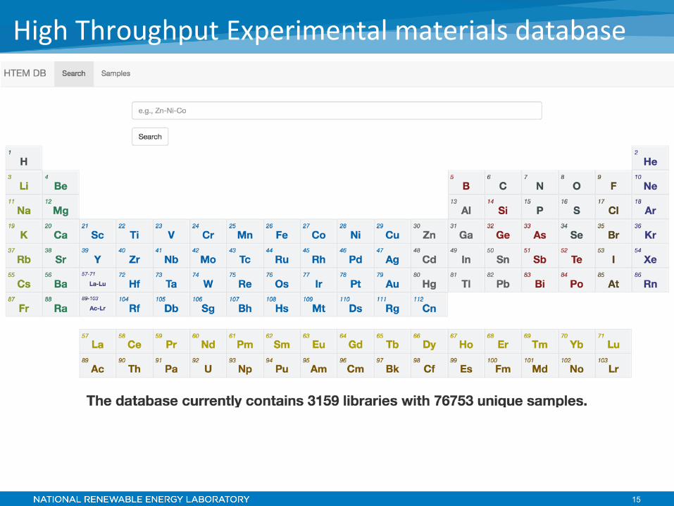
High Throughput Experimental materials database
~30,000 electrical resistances ~40,000 optical absorption spectra
~75,000 compositions,thicknesses ~75,000 x-ray diffraction htem.hpc.nrel.gov (internal)
X-Ray Diffraction
Data
Reflectivity and
Transmission Data
Resistivity and Conductivity
Data
X-Ray Fluorescence
Data
Deposition Data
Curation, Alignment,
Post-processing
Project-Specific
Research Database
REST API
Web-based Analysis and Visualization
Tools
Data Mining and Deep Analysis
Data Interchange with
External Collaborators
MCST Data Warehouse
~ 75,000 samples
~ 1.4 Million Files
Theory: http://materials.nrel.gov/ Experimental Database Under Development

Summary and Conclusions

17
Summary and Conclusions
Summary: what research we do • Novel Thin Films Inorganic PV Materials • Absorbers, Contacts, Interfaces, Devices • Oxides, Nitrides, Sulfides, Selenides • High-Throughput Combinatorial Research Methods • Materials by Design Energy Frontier Research Center • High Throughput Experimental materials database
Conclusions: modes of collaboration • Common materials research interest • Your materials made/studied at NREL • NREL materials studied at University • Student research at (6-12 months) • Postdoc research (3-6 month)
More information: Andriy Zakutayev
[email protected] http://www.nrel.gov/materials-
science/materials-discovery.html