on chopper effects in discrete-time modulatorsdigital.csic.es/bitstream/10261/60025/1/on chopper...
TRANSCRIPT

1
On Chopper Effects in Discrete-Time Σ∆Modulators
Gildas Leger, Antonio Gines, Eduardo J. Peralıas, and Adoracion Rueda, Senior, IEEE
Abstract—Analogue to Digital converters based on Σ∆ mod-ulators are used in a wide variety of applications. Due totheir inherent monotonous behavior, high linearity and largedynamic range they are often the preferred option for sensor andinstrumentation. Offset and Flicker noise are usual concerns forthis type of applications and one way to minimize their effectsis to use a chopper in the front-end integrator of the modulator.Due to its simple operation principle, the action of the chopperin the integrator is often overlooked. In this paper we providean analytical study of the static effects in Σ∆ modulators, whichshows that the introduction of chopper is not transparent to themodulator operation and should thus be designed with care.
Index Terms—Σ∆ modulation, chopper, noise leakage, design.
I. INTRODUCTION
W ITH the ever decreasing feature size of silicon pro-cesses, digital circuits have been implementing more
and more functionality. However, most applications requirean interface to the real world. At some point, an analog-to-digital converter is thus necessary. Due to their relativelylow analog complexity – because part of the conversion isrealized in the digital domain by the decimation filter –Σ∆ converters are often the preferred architecture for high-resolution and low to medium frequency applications. Theseconverters are inherently monotonous and usually exhibit highlinearity. Although in the past few years continuous timeΣ∆ modulators have been introduced to extend the marketto higher frequency range, discrete time modulators – mainlybased on switched-capacitor techniques – gather the major partof the instrumentation and audio market. These converters canreach very high resolutions (up to 24bits). At this level, anysource of noise becomes a concern. This is particularly trueat low frequency, where Flicker noise is a limiting factor. Forsensor applications where calibration is not possible, the mainconcerns when using a Σ∆ converter may be Flicker noise,gain and offset errors. There are two main techniques that canbe used to reduce offset and Flicker noise. These are correlateddouble sampling (CDS) and chopping [1].
It is well known that Σ∆ modulators are very sensitiveto the non-idealities of the front-end integrator. Indeed, for
(c) 2010 IEEE. Personal use of this material is permitted. Permission fromIEEE must be obtained for all other users, including reprinting/ republishingthis material for advertising or promotional purposes, creating new collectiveworks for resale or redistribution to servers or lists, or reuse of any copyrightedcomponents of this work in other works.
This work has been partially funded by the Spanish Government projectTEC-2007-68072 and the CSIC project 200850I213.
The authors are with the Instituto de Microlectronica de Sevilla, CentroNacional de Microelectronica, Consejo Superior de Investigaciones Cientıficas(CSIC) and Universidad de Sevilla, 41012 Sevilla, Spain.
the integrators located further in the loop, the perturbationsinduced by the non-idealities are partially modulated to thehigh frequencies and their contribution to the baseband erroris minimal. CDS and chopping are thus applied only to the firstintegrator in the loop. It has also been proposed in [2] to applychopper to the complete modulator. This requires designing ahigh-pass modulator, which is a fundamental and challengingarchitectural change. For this reason this solution has remainedmarginal.
Beyond offset and Flicker noise suppression, CDS techniquebased on Nagaraj’s integrator [3], [4] has the advantage ofrelaxing amplifier DC gain requirements. The use of such anintegrator in Σ∆ modulators has been contemplated in [5]. In[6] a noise analysis of the integrator is performed, which showsthat the input capacitance of the amplifier should be minimizedto effectively cancel Flicker noise contribution. Despite theimportant benefits of this integrator structure, its use in Σ∆modulators is not generalized because it requires specific andcareful design.
On the other hand, chopping seems to be a much morestraightforward approach. Apparently, it can be included inan existing integrator design with little effort. As a matter offact, the papers describing modulators that include choppingseldom detail chopper implementation and its possible impacton performance [7]–[9]. Neither do reference textbooks [10],[11] or studies on non-ideality modeling [12], [13]. In arecent paper [14], the authors propose to use a pseudorandomchopping sequence and extend the results of [1] to estimatethe residual offset due to switch charge injection.
This paper studies the chopper static effects in the front-end integrator of Σ∆ modulators, and will show that chopperimplementation is not as straightforward as it seems.
The paper is organized as follows: Section 2 is devoted tothe chopper operation in the integrator. A high-level event-driven model is proposed and validated. Section 3 provides adetailed study of chopper effects in Σ∆ modulators. Section 4points out the peculiarity of high-level simulations. Section 5presents transistor level simulations that validate the analyticalstudy and Section 6 provides some practical considerations forthe designer to account for the referred effects. Finally Section7 summarizes the paper conclusions.
II. THE CHOPPED INTEGRATOR
Two main implementations of the chopped integrator can befound in the literature. The first and most direct one consists inflipping the amplifier by adding crossed switches in series atits inputs and outputs, as illustrated in Fig.1-a. In that way, the

2
1d
2d
1
2 d
c
C1
C2
VX+
2C1
1
2d
1d
d
c
C2
d
c
d
c
1 1d
c , A
VY+
VY-
VX-
VU+
VU-
2 2d
2d A
1
2C1
C2
2d B
1d A
1d B
1d A
1d B
2d B
2d A
1
2
AB
BA
AB
BAC1
C2
VU+
VU-
VX+
VY+
VY-
VX-
d , B
a)
b)
c)
Fig. 1. a) Diagram of a single-branch integrator with a chopped amplifier.b) Diagram of a chopped integrator, where the chopping is implemented onthe feedback capacitors and the integrator input. c) Integrator clock phases.
noise and offset introduced by the amplifier are modulated bythe chopper signal. The chopper transitions (controlled by φcand φd) occur in the interphase between φ1 and φ2 as shownin Fig.1-c. For this implementation, the chopper transitionscould also be located during the sampling phase φ1 to limitadditional noise sampling as proposed in [8]. However, theamplifier would have less time to properly settle and thismay induce a signal-dependent error, particularly if the nextintegrator also samples on phase φ1.
In the second implementation of the chopped integrator[15], represented in Fig.1-b, the integrating capacitances areflipped instead of the amplifier, which also requires to applythe chopper to the integrator inputs. The first order resultsare identical to those of the first implementation. The maindifference between the two schemes actually lies in dynamicsettling requirements that have no contribution to the staticbehavior.
For a classical integrator without chopping (consider φc = 1and φd = 0 in Fig.1-a), the contribution of the amplifier offsetVoff to the integrator output VU can be calculated as,
VU ≈b(1− b+1
A
)z−1 (Vin − Voff )
1− z−1(1− b
A
) (1)
Vin = VX − VYwhere b = C1/C2 and A is the amplifier DC gain.
For a chopped integrator, it is usual to consider that theoffset term Voff in (1) is simply replaced by its modulated
d
c
C2
d
c
d
c
d
c
Cpn
CpiCpo
Cpn
Cpp
C2
Cpp
A
B
+
-
-A x
(V
I-Vof
fc )
VI
VU
*
VU+*
VU-*
Fig. 2. Integrator schematic during a chopper transition, including theparasitic capacitors on the amplifier.
version V coff . We have,
Voff → V coff = Voff ∗ CH (z) (2)
where CH (z) is the z-transform of the two-valued choppingsequence ch (n) (either 1 or −1) that represents the amplifierflipping action controlled by phase φc and phase φd.
A. Effect of chopper transitions
Let us consider the instant at which the chopper flips thesignal paths, in other words a rising or a falling edge of thechopper signal. This chopper transition occurs in the interphasebetween φ2 and φ1. As both phases are low, the connectionto the sampling capacitors is open and the two architecturesrepresented in Fig.1 reduce to the same case study with respectto chopping effects. The integrator schematic during a choppertransition is shown in Fig.2. The parasitic capacitors thatmay affect the integrator operation during a chopper transitionhave also been represented. There is an input capacitor Cpi,an output capacitor Cpo, a positive feedback capacitor Cppand a negative feedback capacitor Cpn. For these last twocapacitors, a differential contribution is considered for the sakeof simplicity. Indeed, if the parasitic occurs on a single branchit will affect both the common-mode and the differentialsignal. The differential contribution can be calculated takingone half of the single branch capacitor value.
Neglecting settling and charge injection mechanisms in theswitches, it is obvious that the output capacitor Cpo has noeffect since it is connected to a voltage source. The chargeconservation equations at nodes A and B in Fig.2 lead to themodified integrator output V ∗U after a chopper edge,
V ∗U =
[1 +
Cpp−CpnC2
+ 1A
(1− Cpp+Cpn+Cpi
C2
)]VU − 2V coff
1− Cpp−CpnC2
+ 1A
(1− Cpp+Cpn+Cpi
C2
)(3)
where VU is the integrator output before the chopper edge,given by (1).
Equation (3) can be simplified by neglecting the terms di-vided by A and considering the offset term small with respectto the integrator output range. In this way and considering

3
parasitic capacitances smaller than C2, a first order Taylordevelopment of (3) gives,
V ∗U ≈ (1 + δ)VU − 2V coff (4)
δ = 2Cpp − Cpn
C2
Hence, each time that the chopper flips the amplifier, theintegrator output voltage will be slightly scaled up or down(depending on the value of Cpp and Cpn). This is not the casein an integrator without chopper since these parasitic capaci-tors simply add up to the feedback capacitor C2, and wouldappear as an integrator gain error similar to the conventionalcapacitor mismatch.
The presence of an offset in the amplifier imbalances thevirtual grounds, and the charge required to recover the equi-librium (which has to be drawn from the feedback capacitorC2) modifies the integrator output. There is thus an offsetcomponent related to the chopper transitions, in addition tothe conventional one already shown in (2). It can be seen in(3) that the parasitic capacitors also modify the coefficient ofthis offset contribution. However, for low offset values thiscan be considered as a second order effect.
B. A high-level model of the chopped integrator
We have seen above that beyond the classical choppermodulation effect, there are two spurious contributions tothe integrator output that are related to chopper transitions(i.e. the amplifier flipping events). One is an additional offsetcontribution and the other is a parasitic contribution thatmodulates the integrator output. These two contributions addto the output samples following a flipping event.
In order to validate (4), we performed transistor-level simu-lations of an integrator designed in AMS 0.35µm technology.The gain of the integrator is b = 0.5.
First of all, a 10mV voltage source has been introducedin series with one of the amplifier inputs. We performedthree transient simulations for three different values of thechopper frequency fch = fs/(2M): M=1, M=2 and M=5. Theintegrator input was set to 0 to see only the offset contributionat the integrator output. Fig.3 displays the obtained results. Itcan be seen that the integrator output follows the expectedbehavior: the offset is modulated by a square wave andintegrated, but we can also see a component due to the choppertransitions. The classical chopper component, as described in(1) and (2), leads to a step at the integrator output at eachsample period of,
stepCH = b× Voff = 0.5× 0.01V = 0.005V (5)
While the transition component, as expressed in (4), leadsto an additional increase of,
stepCT = 2× Voff = 2× 0.01V = 0.02V (6)
This component has to be summed to the classical one,that is why a positive or negative step of 0.025V is observedat each chopper transition, for the three chopper frequencies.Notice that the first transition must not be taken into account
0 0.2 0.4 0.6 0.8 1
x 10-5
-0.01
0
0.01
0.02
0.03
0.04
time (in s)
inte
grat
or o
utpu
t (in
V)
M=1
M=2
M=5 stepCH
stepCT
+
stepCH
Fig. 3. Integrator output for a 0V input in the presence of a 10mV amplifieroffset. The transient simulation has been realized for three different chopperfrequencies fch = fs/(2M): M=1, M=2 and M=5.
0.0125V
10 15 20 25
0
0.5
1
1.5
time (in s)
inte
grat
or o
utpu
t (in
V)
no chopperM=1M=2M=3M=5
0.0125V
0.0125V 0.0125V
Fig. 4. First integrator impulse response for different chopper frequencies.
because it corresponds to the integrator initial state for whichthe feedback capacitors are discharged and thus do not holdthe offset value.
In order to validate the second spurious contribution (theeffect of parasitic capacitors during chopper transitions), theoffset has been set to 0 and a positive feedback capacitor hasbeen introduced around the first amplifier (Cpp = 10fF inFig.2). The feedback capacitance C2 is made of four unitcapacitors of 400fF . Accordingly to (4) we have,
δ = 210× 10−15
4× 400× 10−15= 0.0125 (7)
The integrator response to a Vin = 2V impulse has beensimulated. For an ideal integrator of gain b = 0.5, the responseshould be a step signal of 1V . Amplifier finite DC gain willproduce a slow decay of the integrator output, while chopperparasitic effect should give rise to periodic incremental stepsof δbVin for each chopper transition.
Fig.4 shows the impulse response obtained for five differentcases: in the absence of chopper and for a chopper at fs/2,fs/4, fs/6 and fs/10 (i.e. M = 1, 2, 3, 5).
4
IN(z)
CH(z)
U(z)
1z
1
1
1z
Ab
b
OFF(z)b
2
5.0
CT(z)
Offset contribution
Parasitic contributionOF
FC
T
OFFCH
Fig. 5. High level model of a chopped integrator for event-driven simulators,including chopper transition effects.
It can be clearly appreciated how the integrator output isincreased by the effect of chopper and that the incrementalsteps occur every 1, 2, 3 and 5 samples as expected. Theincrements are also of the expected value: δbVin ≈ 0.0125V .The step value actually increases as the integrator outputincreases from its initial value of bVin = 1V . For theintegrator without chopper there is actually a slight decreaseof −4× 10⁻⁵V that corresponds to the pole error induced bythe amplifier finite DC gain.
These electrical simulations show that the chopped inte-grator behaves as predicted by (4), and hence we can usethis equation to build a high level event-driven model tofacilitate further investigations on the impact of choppedintegrators on discrete-time signal processing circuits, such asΣ∆ modulators.
To build this model, we need to analytically define thechopper transition signal. Let us consider the chopper signal,ch(n) as a two valued signal (1 and -1). On other hand, thechopper transition signal, ct(n), must be equal to 1 for thesample immediately following a chopper rising or falling edge,and 0 elsewhere. This signal can be built from the choppersignal as,
ct(n) = (1− ch(n)ch(n− 1)) /2 (8)
The chopped integrator model based on the modulationeffect described in (4) can thus be built as shown in Fig.5.
Signal IN is the integrator input and U is its output. Wecan readily separate the two spurious contributions highlightedin (4) at the summing node of the integrator: one related tothe offset and the other to the integrator output modulationdue to the parasitic capacitors. To generate the former, signalOFF accounts for the offset and Flicker noise of the amplifier.It is multiplied by the chopping sequence CH to generatethe classical chopper component (OFFCH ) and also by thechopper transition signal CT to generate the chopper transitioncomponent (OFFCT ). To generate the latter, the integratoroutput U is modulated by the chopper transition signal andscaled by the parasitic factor δ.
Ivirtual
X
Y
Loop Filter
First Integrator
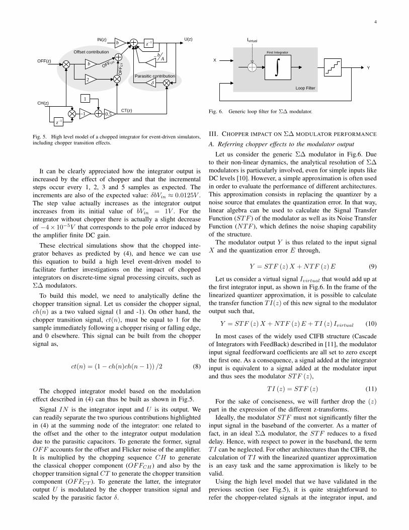
Fig. 6. Generic loop filter for Σ∆ modulator.
III. CHOPPER IMPACT ON Σ∆ MODULATOR PERFORMANCE
A. Referring chopper effects to the modulator output
Let us consider the generic Σ∆ modulator in Fig.6. Dueto their non-linear dynamics, the analytical resolution of Σ∆modulators is particularly involved, even for simple inputs likeDC levels [10]. However, a simple approximation is often usedin order to evaluate the performance of different architectures.This approximation consists in replacing the quantizer by anoise source that emulates the quantization error. In that way,linear algebra can be used to calculate the Signal TransferFunction (STF ) of the modulator as well as its Noise TransferFunction (NTF ), which defines the noise shaping capabilityof the structure.
The modulator output Y is thus related to the input signalX and the quantization error E through,
Y = STF (z)X +NTF (z)E (9)
Let us consider a virtual signal Ivirtual that would add up atthe first integrator input, as shown in Fig.6. In the frame of thelinearized quantizer approximation, it is possible to calculatethe transfer function TI(z) of this new signal to the modulatoroutput such that,
Y = STF (z)X +NTF (z)E + TI (z) Ivirtual (10)
In most cases of the widely used CIFB structure (Cascadeof Integrators with FeedBack) described in [11], the modulatorinput signal feedforward coefficients are all set to zero exceptthe first one. As a consequence, a signal added at the integratorinput is equivalent to a signal added at the modulator inputand thus sees the modulator STF (z),
TI (z) = STF (z) (11)
For the sake of conciseness, we will further drop the (z)part in the expression of the different z-transforms.
Ideally, the modulator STF must not significantly filter theinput signal in the baseband of the converter. As a matter offact, in an ideal Σ∆ modulator, the STF reduces to a fixeddelay. Hence, with respect to power in the baseband, the termTI can be neglected. For other architectures than the CIFB, thecalculation of TI with the linearized quantizer approximationis an easy task and the same approximation is likely to bevalid.
Using the high level model that we have validated in theprevious section (see Fig.5), it is quite straightforward torefer the chopper-related signals at the integrator input, and

5
therefore at the modulator output (taking into account theintegrator gain b). As explained above, there are two distinctcontributions: one is the offset and Flicker noise contribution(OFFchop), and the other is a modulation of the integratoroutput due to the parasitic coupling between the amplifierinputs and outputs (Pert).
The offset contribution can be calculated as,
OFFchop = TI × OFFCH +OFFCTb
(12)
= TI × b OFF ∗ CH + 2OFF ∗ CH ∗ CTb
where we have separated the classical chopper componentOFFCH and the chopper transition component OFFCT . Forthe sake of simplicity, we consider both amplifier Flicker noiseand offset in the term OFF .
The parasitic contribution is written as,
Pert = TI × δ
b[U1 ∗ CT ] (13)
where U1, the z-transform of the first integrator output, ismodulated by the chopper transition signal CT .
Let us study separately the impact of these two perturba-tions.
B. Offset and 1/f noise contribution
Obviously, the chopper transition signal ct(n) is quitedifferent from the chopper signal ch(n). Let us study howit modifies offset and Flicker modulation. It is important toremark that the chopper transition component (OFFCT inFig.5) is multiplied by both the chopper signal (ch) and thechopper transition signal (ct). We have,
offct (n) = 2off (n)× ch (n)× ct (n) (14)m
OFFCT = 2OFF ∗ CH ∗ CT
The spectrum of the chopper transition signal cannot beknown a-priori but it is deterministically linked through (8)to the chopper signal. This introduces a direct simplification.Because ch(n) is a square signal between 1 and −1, we havech(n)2 = 1, which leads to,
offct = 2off (n)× ch (n)× ct (n) (15)= off (n)× (ch (n)− ch (n− 1))
mOFFCT = OFF ∗
[(1− z−1
)CH
]Hence, the total chopped offset and Flicker noise contri-
bution referred to the modulator output, as shown in (12),simplifies to,
OFFchop = TI ×OFF ∗[(
1 + b− z−1
b
)CH
](16)
Depending on the chopping signal nature, the frequencyshaping related to the chopper transition contribution can bemore or less relevant. As an example, [16] proposes to usea frequency-shaped pseudo-random chopper signal. A white
10-3
10-2
10-1
-120
-100
-80
-60
-40
-20
0
normalized frequency
chop
ped
offs
et p
ower
spe
ctru
min
dB
(re
ferr
ed to
the
off
set)
chopper transitions component
classical chopper component
overall chopper
Fig. 7. Chopper effect on the offset, including classical chopper componentand chopper transition component. The chopper is a pseudo-random sequenceshaped as defined in [16].
sequence from an LFSR is sent to a simple digital modulatorwhose transfer function has a zero at DC and another at fs/2.The first one minimizes the power in the baseband while thesecond one limits possible coupling of high-frequency tones onthe full-scale voltage references. We generate such a sequencein Matlab and use it in our model to examine the impact ofthe chopper transition signal. Without much loss of generality,we neglect the filtering action of the architecture-specific termTI , as discussed above.
Fig.7 shows the chopped-offset spectrum normalized to theoffset power. A total of 100 spectrums computed over 2048samples have been averaged in order to reduce variability. TheFFTs were calculated using a high performance window (aRife-Vincent type-2 window, with 165dB side-lobe attenuation[17]) to avoid any spectral leakage. Together with the overallresult (the thick line), we have represented the classicalchopper component (with square markers) and the choppertransition component (with round markers). The shaping effecton the latter can clearly be appreciated. At low frequency, theclassical chopper component dominates the noise spectrum. Athigh frequency, the chopper transition component significantlyincreases the noise power level. In particular, the power densityat fs/2 is 14dB higher than expected from the classicalchopper component.
If Flicker noise is the main concern, the signal OFF in (16)cannot be considered as a scalar. Actually, its power spectraldensity is of the form,
SOFF ∝1
f(17)
and the analytical resolution of the convolution in (16) is notstraightforward.
To illustrate its effect, Fig.8 shows the chopped-Flickerspectrum in the same way as in Fig.7. The power spectrumof the Flicker noise without chopper is also represented inorder to illustrate the benefits of chopping. It can be seen howchopping effectively brings a reduction of Flicker noise powerat low frequency. As expected, the zeros at DC and fs/2 that

6
10-3
10-2
10-1
-50
-40
-30
-20
-10
normalized frequency
pow
er s
pect
rum
(in
dB
FS
)
overall chopper
input flickerclassical chopper componentchopper transitions component
Fig. 8. Effect of chopper transitions on the spectrum of the choppedFlicker noise referred at the integrator input. The chopper is a pseudo-randomsequence shaped as defined in [16].
could be seen in Fig.7 for a DC offset are significantly filledby Flicker noise aliasing.
In significant contrast to the DC offset case, it can beseen that the chopper transition component dominates overthe classical chopper component on the entire spectrum andnot only at high frequency. In particular the power spectraldensity of the overall chopped Flicker noise is close to 10dBhigher than what could be expected with a simple model at lowfrequencies. This increment is significant and should thus betaken into account during the design phase in order to definea correct design margin for the amplifier Flicker noise, whichdirectly impacts on the minimum size of its input transistors.
C. Parasitic contribution
This section analyzes the impact of the parasitic capacitorsthat modulate the integrator output, as introduced in (13).
In order to go further in the analysis, we need to develop theterms TI , U1 and CT . The first two depend on the particulararchitecture of the Σ∆ modulator. The first integrator of Σ∆modulators is usually fed with the difference between the inputsignal and the output bitstream. Taking (9) into account, theoutput of the integrator (U1) can thus be written,
U1 =bz−1
1− z−1((1− STF (z))X −NTF (z)E) (18)
For the sake of simplicity, in what follows we will considerthe case study of an architecture that implements an ideal Lth
order modulator such that,
STF (z) = TI (z) = z−L (19)
NTF (z) =(1− z−1
)LIn this case, the expression of the perturbation (13) can be
written as,
Pert = δz−L ×
[CT ∗
((L−1∑i=0
z−i
)X
)](20)
−δz−L ×[CT ∗
(z−1
(1− z−1
)L−1E)]
From this equation, it can be seen that the perturbation hasa signal-dependent term and a noise-dependent term.
For any particular architecture, TI and U1 should be calcu-lated, but the perturbation will likely be similar to (20); thatis, a signal and a noise contribution modulated by the choppertransition signal.
As both noise and signal are convoluted by the choppertransition signal CT , its spectrum is particularly relevant tounderstand the impact of the chopper parasitics. Up to thispoint, the type of chopper signal (and consequently the chop-per transition signal) has not been specified. Let us considerthree cases.
1) Chopping at fs/2: When the chopper frequency is setto half the sampling frequency, the amplifier is flipped ateach period. All the samples will get the chopper transitioncontribution. As a result the chopper transition signal is,
CT (z) = 1 (21)
Hence, the signal and noise contributions of the perturbationare not modulated. While the signal contribution simply addsup to the nominal signal, the noise contribution will degradeperformance. It can be seen from (20) that some quantizationnoise shaped at order L− 1 will leak into the baseband.
For this particular case, it is interesting to come backto the integrator level expression given in (4). Indeed, as achopper transition occurs at each period, the chopper parasiticcontribution appears as a pole error, just like the effect ofamplifier finite DC gain. The impact of a pole error in thefirst integrator on the modulator performance is well known[10], [12]. It is important to notice that, unlike for the amplifierDC gain, the sign of the chopper induced pole error dependson the parasitic capacitances. This can be particularly relevantfor stability concerns [18].
The expected power spectral density Spert of the noise termof the perturbation can be calculated analytically. For that, wehave to develop the squared modulus of the second term in(20). Under Bennett’s conditions, the quantizer error E can beapproximated to a white noise of power spectral density,
SE =∆2
12fs(22)
where ∆ is the quantizer step and fs the sampling frequency.It comes,
Spert = 2δ2∆2
12fs
(1− cos
(2π
f
fs
))L−1(23)
This coincides with the classical result obtained for integra-tor pole error in single stage Σ∆ modulators [10].
2) Chopping at lower frequencies: It is often recommendedas a good design practice to isolate the voltage referencesthat define the modulator full-scale from any signal at fs/2,[10]. Such a coupling would likely demodulate high powertones from the quantization error into the baseband. Hence,one could operate the chopper at a frequency lower than fs/2in order to avoid the introduction of a clock signal at fs/2,like for instance in [7]. However, if the chopper is operated atfrequencies lower than fs/2, the chopper transition signal isno longer constant and noise folding occurs.

7
Let us consider a chopper frequency of fs/(2M), whereM is an integer higher than 2. In order to avoid harmonics atfs/2, M should also be odd, but our study is valid for bothodd and even values. The chopper transition signal definedabove is thus of the form,
ct (n) = 1 for n = kM with k ∈ ℵ (24)= 0 otherwise
Calculating CT (z) from the definition of the z-transform isnot straightforward. Instead, we can remark that multiplyingthe integrator output by the chopper transition signal is equiv-alent to downsample and then upsample by a factor M . Sucha combination is widely used in multirate analysis and we canthus build on these results.
According to [19], the z-transform of the integrator outputmultiplied by the chopper transition signal can be written as,
CT (z) ∗ U (z) =1
M
M−1∑k=0
U(zej
−2kπM
)(25)
The perturbation spectrum (13) can thus be expressed as asum of the integrator output spectrum components shifted bykfs/M . This aliasing is due to the downsampling, while thescaling by 1/M is due to the upsampling.
To go further and describe the impact of the perturbationin a better way, we can consider an ideal Lth order CIFBmodulator, which is what led us to (20). In this case, theperturbation can be written as,
Pert =δ
Mz−L
M−1∑k=0
(L−1∑i=0
z−iX
)z→ze−j2π
kM
(26)
− δ
Mz−L
M−1∑k=0
(z−1
(1− z−1
)L−1E)z→ze−j2π
kM
The first term shows that the perturbation contains aliasesof the modulator input signal around the frequencies kfs/M .Taking into account that in the majority of cases, the modulatorOSR is much higher than the modulator order L, the inputsignal X can be considered as a low-frequency and we canmake the following approximation,
OSR >> L⇒L−1∑i=0
z−iX ≈ LX (27)
Furthermore, for moderate values of M the input signalbandwidth is also likely to be inferior to fs/(2M) and thus,no overlapping of the aliases should occur. In this case, thepower spectrum of the perturbation signal part can be easilycalculated as,
Ssig =
(δL
M
)2M−1∑k=0
∥∥∥X (ze−j2π kM
)∥∥∥2 (28)
If the OSR of the modulator is large, the signal aliasesshould be correctly suppressed by the decimation filter, andits impact on the modulator performance should be limited.However, Σ∆ modulators are often touted for their low anti-aliasing requirements. If high frequency and high power toneswere present in the modulator input signal, they could leak
10-4
10-3
10-2
10-1
-100
-80
-60
-40
-20
normalized frequency
pow
er s
pect
rum
(in
dB
FS
)
CH
CT
Fig. 9. Power spectra of the chopper signal (CH) proposed in [16], and ofits associated chopper transition signal (CT).
into the baseband. This part of the perturbation should thusnot be completely overlooked.
The second term in (26) is related to the modulator quan-tization noise. Considering that the aliases of the quantizationerror are uncorrelated, the power spectral density can becalculated as,
Snoise =
(δ
M
)2
SE
M−1∑k=0
∥∥∥1− e−j2π( ffs− kM )∥∥∥2(L−1) (29)
=
(δ
M
)2
SE4L−1M−1∑k=0
sin2(L−1)(π
(f
fs− k
M
))=δ2
MSE
(2 (L− 1))!
(L− 1)! (L− 1)!
It comes that for any Lth order modulator that implementsan ideal NTF of the form
(1− z−1
)L, the quantization noise
folding due to chopper modulation should have a flat powerspectrum. The total perturbation power that falls into themodulator baseband can thus be easily calculated, taking (22)into account:
for M ≥ 2, (30)
Pnoise =δ2
M
∆2
12OSR
(2 (L− 1))!
(L− 1)! (L− 1)!
The particular case M = 1 corresponds to the chopperoperated at the Nyquist frequency and has been treated in theprevious sub-section.
3) Random chopping: The developments carried out for thechopper operated at a frequency lower than fs/2 allow us toforesee what should happen with a random chopping. Indeed,expression (13) remains valid, and the z-domain transform ofthe integrator output will now be convoluted by a a randomsignal. Notice, though, that the chopper transition signal is notthe chopper signal, and the shape of their spectra may be quitedifferent.
This is illustrated in Fig.9, which shows the power spectrumof the chopper signal (CH) proposed in [16] together withthe corresponding chopper transition signal (CT). It can beseen that the chopper transition signal has a spectrum that is

8
0 0.1 0.2 0.3 0.4 0.5-160
-140
-120
-100
-80
-60
normalized frequency
pow
er s
pect
rum
(in
dB
FS
)A=0.002A=0.2
Fig. 10. Perturbation power spectrum for a 2nd order modulator with chopperat fs/4, for two amplitudes of the input sine-wave.
quite different from the chopper signal. Excepting a significantDC component and a tone at fs/2, the spectrum is almostflat. Because the first integrator output is not correlated to thechopper transition signal (at least in first order), we can expectthat the perturbation spectrum will have three contributions.The convolution with the DC component will lead to a scaledreplica of the integrator output. The convolution by the toneat fs/2 will lead to an alias of the integrator output. Andfinally, the convolution with the white noise will lead to awhite noise. In order to calculate a closed form expression ofthe perturbation spectral density an analytical expression ofCT (z) would be necessary.
IV. THE PITFALLS OF HIGH-LEVEL SIMULATION
In order to reach closed form analytical expressions, wehave used a well-known but strong approximation: modelingthe quantization error E as a white noise source. The validityof this approximation is quite limited for Σ∆ modulators,particularly those that rely on a single-bit quantizer.
In order to illustrate this assertion, we perform a high-levelsimulation of a 2nd order modulator like the one presentedin [20], including our chopped-integrator model. A chopperwith a parasitic parameter δ = 0.01 at a frequency of fs/4is considered. Fig.10 shows the spectrum of the perturbation(acquired at the output of the gain block δ in Fig.5) for twodifferent amplitudes of the input sine-wave. It appears clearlythat the noise part of the perturbation spectrum is not flat andthat it is very different in the two cases. There is thus a strongcorrelation between the input signal and the quantizer error E.
In the case of the small amplitude, the perturbation is almostnegligible. This can be better understood taking a look at theintegrator output in the time-domain.
The dashed line with cross markers in Fig.11 shows theintegrator output for a small amplitude sine-wave (there isone marker per sample). The round markers correspond to theintegrator output multiplied by the chopper-transition signal ct,which is the signal that is fed to the integrator input throughthe parasitic capacitor. For input signals close to zero, theintegrator output follows a regular pattern whose period can bea multiple of the chopper transition period. In this particularcase, the samples that coincide with chopper transitions arecasually all close to zero. For that reason, the perturbation
2000 2010 2020 2030
-0.6
-0.4
-0.2
0
0.2
0.4
0.6
sample
inte
grat
or o
utpu
t (n
orm
aliz
ed t
o F
ull-S
cale
)
u1(n) u1(n) x ct(n)
Fig. 11. Integrator output for a small amplitude input sinewave.
0 0.1 0.2 0.3 0.4 0.5-90
-85
-80
-75
-70
-65
-60
normalized frequency
pow
er s
pect
rum
(d
BF
S)
M=2
M=3
M=7
M=13
M=2M=3
M=7
M=13
0 0.1 0.2 0.3 0.4 0.5-95
-90
-85
-80
-75
-70
-65
-60
-55
normalized frequency
pow
er
spec
trum
(in
dB
FS
)
M=2
M=3
M=7
M=13
M=2M=3M=7M=13
a)
b)
Fig. 12. Perturbation spectra for four chopper frequencies. These spectrahave been produced by averaging the FFT of the perturbation signal for 1000input sine-waves with a fixed amplitude but random DC level and phase.The modulator is a 2nd order a) with a single-bit quantizer, b) with a 2-bitquantizer.
power is much lower than expected because the chopper doesnot capture the ”noisy” component of the integrator output.
In order to get rid of the input signal correlation, we canperform 1000 simulations of the modulator for 1000 inputsine-waves of identical amplitude and frequency but randomDC level and random phase. By averaging the FFT results(computed with a Rife-Vincent window, over 1024 samples)for the 1000 sine-waves, we make the average correlationbetween the integrator output and the chopper transition signal

9
almost negligible. This allows retrieving a general trend in theperturbation that should be valid for realistic inputs (i.e. nonpure tones). Fig.12-a shows the average spectrum obtained forfour different chopper frequencies fs/(2M). The thick graylines labeled on the right side of the figure represent the flatspectral density level that was expected according to (29).
Notice that the tones correspond to the signal part of theperturbation. The input signal is modulated at kfs/(2M), butonly the DC level contribution can be appreciated because thesmall sine-wave amplitude (-60dBFS) falls below the noisefloor.
It can be seen that the perturbation spectrum is still not trulyflat for M = 2 and M = 3. The spectra present a valley atlow frequency. This implies that the perturbation power in thebaseband is lower than specified in (30) for low values of M .For M = 7 and M = 13, the perturbation spectra are muchflatter, and (29) only overestimates the perturbation power in1dBFS approximately.
The second order single-bit modulator chosen for the simu-lation exhibits strongly non-linear dynamics. It is well-knownthat Bennett’s conditions are better fulfilled for higher ordermodulators, multi-bit quantizers or by the use of dithering.To illustrate this, we performed the same simulation on thesame 2nd order architecture but with a 2-bit quantizer. Fig.12-b displays the obtained results. It can be seen that in this case,the matching of the power spectra with (29) is almost perfect.
Two conclusions can be drawn from these simulations.The first one is that the closed-form expressions proposed inprevious subsection are correct while the linearized quantizerapproximation holds. When this approximation does not hold,they still give a good insight into the expected behavior,but high-level simulations would give more accurate results.The second conclusion is that some care must be taken withhigh-level simulation to ensure that we are not consideringa particular case which would lead to underestimating theimpact of chopper. Fortunately, with our event-driven modelsuch simulations are computationally inexpensive and severalcases can easily be explored.
V. ELECTRICAL VALIDATION
We have already studied static effects in chopped integra-tors, and verified that the analytical developments allow usto lay down a high level model for further investigation ofchopper effects in discrete-time Σ∆ modulators. This sectioncloses the validation loop and presents electrical simulationsof a complete modulator with chopper.
For this purpose, we have designed a simple 3rd ordercascaded modulator at transistor level. The schematics shownin Fig.13 makes use of a 0.35µm CMOS technology. Forthe sake of simplicity, the three integrators are identical,with folded cascoded amplifiers of 83dB nominal gain. Allthe switches are balanced CMOS to approximate a signal-independent ON-resistance. The unit capacitor value is 423fF.Capacitor C1 uses 2 unit capacitors and Capacitor C2 uses4. The gain of the integrator (b in Fig.5) is thus 0.5. Themodulator is operated at 2MHz.
Notice that the expressions calculated from (19) hold forsingle-loop modulators. The results are still valid for our
1
2
1
2 d
c
C1
C2
Xin+
Xin-2C1
1
2
1
d
c
C2
d
c
d
c
REF+ REF-
REF- REF+
1
2
1
2C1
C2
2C1
1
2
1
C2
REF+ REF-
REF- REF+
Y1
Cpn
Cpn
2
1
2C1
C2
2C1
1
2
1
C2
REF+ REF-
REF- REF+
Y2
1
21
211
11 14
zYYzYzYout
Digital recontruction filter:
Fig. 13. Σ∆ modulator schematic used for electrical simulations.
cascaded modulator, but the order of the modulator (L = 3)has to be replaced by the order of the first stage (L1 = 2).
The reconstruction filter (whose transfer function is quotedin Fig.13) combines the output bit-streams of the two stagesto give the final modulator output. It is implemented as apost-processing task in order to keep the electrical simulationcomplexity as low as possible.
The effects described in this paper are particularly relevantfor low-frequency, high-resolution applications. In order toreach a high resolution, the oversampling ratio (OSR) mustbe high. Combined with the fact that we want to resolveat least 256 FFT bins in the baseband, this leads to longtransient simulation. Furthermore, very high accuracy settingsmust be considered to avoid arithmetic errors that wouldcorrupt the results. Simulation times to reach 18 bit accuracywould be overwhelmingly long on our hardware. In order topresent several simulation results, we preferred to considera lower 16 bit resolution, typical in the audio market. Thisresolution is achieved with an OSR of only 64, and thus atransient simulation of only 256×64×0.5µs = 8.3ms can beconsidered. In order to validate our study, we have to choose aparasitic capacitor (and thus the parameter δ) sufficiently largesuch that the perturbation be visible in the output spectrum.Using (30), we can calculate that a parasitic parameter ofδ = 4.6 × 10⁻³ would lead to a resolution of 11.3 effectivebits (ENOB) at an OSR of 64 and for a chopper operatedat fs/8 = 250kHz (i.e. M = 4). This value should thusbe sufficient to clearly notice the perturbation in the outputspectrum. Taking into account the value of the integratingcapacitor C2, a parasitic capacitor Cpn = 3.9fF is obtained.For our 0.35µm technology, such a parasitic may arise froma parallel routing of 50µm metal lines, as can be found in asignal bus. It is thus a realistic value.
With these parameters, we finally perform four differenttransient simulations of the modulator shown in Fig.13 in-cluding the parasitic capacitor. The simulator is Spectre in aCadence Framework and uses the Bsim 3v3 models providedby the foundry. The accuracy option is set to ”conservative”,but the relative error is calculated with respect to global

10
Modulator output spectrum (electrical simulation)
Perturbation spectrum (high-level simulation)
Quantization noise and perturbation (analytical expressions)
10-4
10-3
10-2
10-1
-150
-100
-50
0
normalized frequency
pow
er
spec
trum
(in
dB
FS
)
OS
R=
64
OS
R=
64
10-4
10-3
10-2
10-1
-150
-100
-50
0
pow
er s
pect
rum
(in
dB
FS
)
OS
R=
64a) b)
c)
10-4
10-3
10-2
10-1
-150
-100
-50
0
normalized frequency
OS
R=
64d)
10-4
10-3
10-2
10-1
-150
-100
-50
0
ENOB=16.2 ENOB=14.7
ENOB=11.3 ENOB=11.2
Fig. 14. Power spectrum of the modulator output obtained from electrical simulation. a) without chopper, b) with chopper at fs/2 (M = 1), c) with chopperat fs/8 (M = 4), d) with random chopper as proposed in [16].
signals instead of local signals, which greatly speeds up thesimulation while maintaining the desired 16bit accuracy. Thefirst simulation is done without chopper, the second in theparticular case of a chopper operated at fs/2 (i.e. M = 1),the third with a chopper operated at fs/8 (i.e. M = 4) andthe fourth with a random chopper as proposed in [16].
In addition to these electrical simulations, we have also per-formed simple high-level simulations in order to demonstratethat the perturbation approximation is reliable enough to takedesign decisions. More concretely, we have simulated an idealmodel of the modulator architecture without chopper, for aninput sine-wave of the same characteristics as for the electricalsimulation and for the same number of samples (64 × 256).The chopper transition signals (ct) for the four cases describedabove have also been generated. This is straightforward forthe first three cases and only the random chopper requires aspecific simulation of the random sequence.
In this way, the expected perturbation can be built multi-plying the ideal integrator output by the chopper transitionsignal and scaling the result by δ. As high-level simulation
is almost inexpensive in terms of CPU time, the process isrepeated 100 times, varying the phase of the input sine-wave.The FFT outputs are averaged in order to reduce spectrumvariability. We could have built-up the high-level simulationswith the proposed chopped-integrator model, but the selectedapproach validates the perturbation approximation that havebeen made for the analytical developments.
Fig.14 displays the obtained results. For all FFTs, the samehigh performance window as previously has been used. For thefirst case (a), there is no expected perturbation since there isno chopper. It can be seen that there is a white noise floorthat limits the resolution of the modulator. This is due toarithmetic errors of the simulator, as explained above. Forthe second case (b), the perturbation appears to be shapedto a first order, as expected, taking into account that the firststage of the modulator is of order L1 = 2. The analyticalexpression of the expected power density, according to (23),is also represented by a dashed line. The matching is almostperfect in the baseband, where the perturbation dominatesthe quantization noise. Notice that operating the chopper

11
at fs/2 may lead to an additional degradation through thecoupling to the voltage references. This effect may outweighthe perturbation but it does not appear here because we usedideal voltage sources for the references. For the third case (c),we also see that the perturbation derived from the ideal high-level simulation almost perfectly match the electrical results.Here again, we have represented by a dashed line the analyticalpower spectral density derived in (30). As commented before,the modulator quantizer is single-bit so the quantization errorcannot accurately be approximated to a white noise, at leastnot for a pure tone input. Anyhow, the analytical expressionstill gives a reliable order of magnitude for the perturbation.Noticeably, the measured ENOB for the electrical simulation is11.3, exactly the expected value calculated using (30). Indeed,the tonal components of the perturbation compensate for theslightly lower noise floor. And for the fourth and last case (c),the high-level simulation of the perturbation perfectly matchesthe electrical results in the baseband. We can see that theperturbation is almost flat, as expected. There is also a signalalias around fs/2 that cannot be clearly seen on the figure dueto the logarithmic scale of the frequency axis. The measuredENOB is 11.2, which is quite similar to the value obtained forthe chopper at fs/8.
For validation purpose, we have considered a parasiticcapacitance of 3.9fF . However, the perturbation theory tellsus that the smaller the perturbation the more accurate theapproximation. Thus, we can be confident that the results forsmaller parasitics will be valid. As a matter of fact, we wouldonly have to scale down the perturbation by the new δ.
So these results are significant in two ways. Not only do theyvalidate our developments but they also show that simple high-level simulations of an ideal model are sufficient to generatean accurate perturbation for different chopper signals andparasitic values.
VI. PRACTICAL CONSIDERATIONS
From the chopped-integrator effects studied in this paperwe can draw some practical implementation considerationsto avoid chopper-related performance degradation in discrete-time Σ∆ modulators. The goal of these guidelines is to helpthe handling of coupling parasitic capacitances effects derivedfrom the chopping scheme that were chosen for the particularapplication. In general, the chopping signal is selected tomeet the requirements of offset and Flicker noise attenuation.Operating the chopper at fs/2 is possibly the most efficientsolution but entails the risk of coupling onto the voltagereferences. Using a lower frequency fs/2M only requires afrequency divider but may lead to more noise folding. Finally,random chopping may completely remove the risk of couplingonto the voltage references but involves more hardware.
In any case,• Consider the use the chopped-integrator model illustrated
in Fig.5 in order to verify the chosen scheme and theimpact of the chopper transition component on the offsetand Flicker noise. The latter is particularly sensitive tofolding.
• Evaluate, either analytically or with high-level simula-tions, the maximum δ that does not cause performance
degradation for your application. Remember that severalsimulations must be performed (for instance with differ-ent input waveforms) to avoid any particular case thatwould underestimate the chopper impact. For example, ifthe objective is to reach 20bits with a 5th order single-loop modulator (i.e. L = 5) with a quantizer of q = 3bits, for an OSR of 64, operating the chopper at fs/4(i.e. M = 2), you must ensure that,
Pnoise ≤1
12 (2ENOB − 1)(31)
which, using (30), reduces to
δ ≤ 2q − 1
2ENOB − 1
√M ×OSR(2 (L− 1))!
= 3.2× 10⁻⁶ (32)
• Calculate the maximum parasitic capacitance that is af-fordable for your design, taking into account the valueof the integrating capacitance. In the above example, anintegrating capacitance as high as 20pF would lead toa maximum parasitic capacitance between the amplifierinput and output as small as 32aF.
• Lay out the chopped integrator taking care of possiblecouplings between the input and output nodes of theamplifier. In particular, avoid crossings of metal lines oradjacent routing in an analog bus. If this is not possible,consider the possibility not to use consecutive metals forthe crossings and a larger separation of the metal linesin the bus. We have seen that 50µm parallel metal linesat minimum separation lead to a parasitic capacitance of3.9fF for the technology that we have used. A minimummetal crossing would give a 85aF capacitance, which isstill 3 times higher than the required value.
• Verify that the extraction rules for your design kit con-sider parasitic capacitances lower than your maximumaffordable parasitic capacitance. If not, you cannot fullyrely on the extractor and you should modify the minimumextracted capacitor. In our case, the minimum extractedcapacitance is 250aF for the default settings, so we hadto calculate the value for minimum metal crossing fromthe technology data.
• Perform extraction of the modulator layout and probe theparasitic between the amplifier input and output nodes.Modify the layout until the parasitics are within yourdesign guard-band.
VII. CONCLUSION
Despite its conceptual simplicity, chopper should not beregarded as the simple addition of four switches around theamplifier. It has been shown in this paper that the introductionof a chopper in the first integrator of a Σ∆ modulatoreffectively modulates the amplifier offset and Flicker noiseout of the base-band. However, these contributions are notsimply modulated by the chopper signal but also by a signalthat depends on the chopper transitions. This must be takeninto account to meet precision requirements, particularly whenthe chopper signal is not a square signal. Furthermore, it hasbeen demonstrated that even a small parasitic capacitance may

12
lead to significant performance degradation due to quantizationnoise demodulation into the base-band. Hence the chopper ina Σ∆ modulator should be designed and laid out with care.
ACKNOWLEDGMENT
The authors would like to thank the reviewers for their veryconstructive comments.
REFERENCES
[1] C. C. Enz and G. C. Temes, “Circuit techniques for reducing the effectsof op-amp imperfections: autozeroing, correlated double sampling, andchopper stabilization,” Proc. IEEE, vol. 84 (11), pp. 1584–1614, 1996.
[2] K. Ishida and M. Fujishima, “Chopper-stabilized high-pass sigma deltamodulator utilizing a resonator structure,” IEEE Trans. Circuits Syst. II,vol. 50 (9), pp. 627–631, 2003.
[3] K. Nagaraj, T. Viswanathan, K. Singhal, and J. Vlach, “Switched-capacitor circuits with reduced sensitivity to amplifier gain,” IEEE Trans.Circuits Syst., vol. 34 (5), pp. 571–574, 1987.
[4] J. A. Grilo and G. C. Temes, “Predictive correlated double samplingswitched-capacitor integrators,” in Proc. Int. Conf. on Electronics, Cir-cuits and Systems ICECS’98, 1998, pp. 9–12.
[5] ——, “The use of predictive correlated double sampling techniques inlow-voltage delta-sigma modulators,” in Proc. Int. Conf. on Electronics,Circuits and Systems ICECS’98, 1998, pp. 149–152.
[6] O. Oliaei, “Noise analysis of correlated double sampling SC integratorswith a hold capacitor,” IEEE Trans. Circuits Syst. I, vol. 50 (9), pp.1198–1202, 2003.
[7] J. M. de la Rosa, S. Escalera, B. Perez-Verdu, F. Medeiro, O. Guerra,R. del Rıo, and A. Rodrıguez-Vazquez, “A CMOS 110-dB@40-kS/sprogrammable-gain chopper-stabilized third-order 2-1 cascade sigma-delta modulator for low-power high-linearity automotive sensor ASIC,”IEEE J. Solid-State Circuits, vol. 40 (11), pp. 2246–2264, 2005.
[8] Y. Yang, A. Chokhawala, M. Alexander, J. Melanson, and D. Hester,“A 114-dB 68mW chopper-stabilized stereo multibit audio adc in5.62mm2,” IEEE J. Solid-State Circuits, vol. 38 (12), pp. 2061–2068,2003.
[9] J. Xuemei, B. Jing, W. Xiaobo, and H. R. Y. Xiaolang, “Aprogrammable-gain chopper-stabilized 2-ordder sigma-delta modulatordesign,” in Proc. Int. Conf. Solid-State and Integrated Circuits Technol-ogy ICSICT’06, 2006, pp. 1785–1787.
[10] S. R. Norsworthy, R. Schreier, and G. C. Temes, Delta-Sigma DataConverters. IEEE press, 1997.
[11] R. Schreier and G. C. Temes, Understanding Delta-Sigma Data Con-verters. John Wiley & Sons, 2005.
[12] F. Medeiro, B. Perez-Verdu, and A. Rodriguez-Vazquez, Top-downdesign of high-performance sigma-delta modulators. Kluwer AcademicPublishers, 1999.
[13] G. Suarez, M. Jimenez, and F. O. Fernandez, “Behavioral modelingmethods for switched-capacitor Σ∆ modulators,” IEEE Trans. CircuitsSyst. I, vol. 54 (6), pp. 1236–1244, Jun. 2007.
[14] H. Chen and J. Chiang, “A Low-Offset Low-Noise Sigma-Delta modu-lator with pseudorandom Chopper-Stabilization technique,” IEEE Trans.Circuits Syst. I, pp. 1–10, Forthcoming.
[15] I. O’Connell and C. Lyden, “A high pass switched capacitor Σ∆modulator,” in Int. Conf. on Electronics, Circuits and Systems, 2002,pp. 307–310 vol.1.
[16] C. B. Wang, “A 20-bit 25-kHz Delta-Sigma A/D converter utilizinga frequency-shaped chopper stabilization scheme,” IEEE J. Solid-StateCircuits, vol. 36 (3), pp. 566–569, 2001.
[17] D. C. Rife and G. A. Vincent, “Use of the discrete fourier transform inthe measurement of frequencies and levels of tones,” Bell System Tech.J., vol. 49, pp. 197–228, 1970.
[18] R. Schreier, “On the use of chaos to reduce idle-channel tones in Delta-Sigma modulators,” IEEE Trans. Circuits Syst. I, vol. 41 (8), pp. 539–547, Aug. 1994.
[19] P. P. Vaidyanathan, “Multirate digital filters, filter banks, polyphasenetworks, and applications: A tutorial,” Proc. IEEE, vol. 78 (1), pp.56–93, 1990.
[20] B. Boser and B. Wooley, “The design of sigma-delta modulation analogto digital converters,” IEEE J. Solid-State Circuits, vol. 23 (6), pp. 1298–1308, 1998.
Gildas Leger received the Physics engineering de-gree from the Institut National des Sciences Ap-pliquees (INSA) of Rennes, France, in 1999 and thePh.D. degree in microelectronics from the Universityof Sevilla, Spain, in 2007.
He is currently holding a position of TenuredScientist at the Instituto de Microelectronica deSevilla (IMSE-CNM-CSIC), Spain.
He has participated in different research projectsfinanced by the European Community and the Span-ish government but also in development projects for
industrial partners. His fields of interest include the design of mixed-signalcircuits and systems, for specific applications like biomedical or space. Moreparticularly, his research focuses on design for testability in the domain ofanalog to digital conversion.
Antonio J. Gines Arteaga received the Physics de-gree in electronics in 2000 from University of Seville(Spain) and joined the Instituto de Microelectrnicade Sevilla (IMSE-CNM-CSIC), where is currentlya researcher. In July 2008, he obtained the Ph.D.degree in microelectronics also from the Universityof Seville.
His current research interests include the design,modeling and testing of CMOS analogue mixed-signal circuits with emphasis on high-speed high-resolution data converters with digital background
calibration and RF front-ends for wireless communications.
Eduardo J. Peralıas Macıas Eduardo J. PeralıasMacıas was born in Seville, Spain in 1964. Hereceived the Licenciado en Fsicas degree in 1992 andthe Doctor en Ciencias Fsicas degree in 1999, bothfrom the University of Seville, Spain. From 1999 to2001, he was with the Departamento de Electrnicay Electromagnetismo at the University of Seville asAssistant Professor. Since 2001, he has been with theInstituto de Microelectrnica de Sevilla (IMSE-CNM-CSIC), where he is currently a Tenured Scientist. Hisresearch interests are in the areas of Mixed Design
with emphasis on Analog-to-Digital converters, Test and Design for Testabilityof Analog and Mixed-Signal Circuits, and Statistical Behavioral Modeling.
Adoracion Rueda obtained the Ph.D. degree in1982 from the University of Sevilla, Spain. From1984 to 1996 she was Associate Professor in thatUniversity, where she now holds the position of Pro-fessor in Electronics. In 1989, she became researcherat the Department of Analog Design of the NationalMicroelectronics Center (CNM), now Institute ofMicroelectronics at Seville (IMSE).
She has participated in many research projectsfinanced by the Spanish government, and by differ-ent programs of the European Community. She has
co-authored many papers in international journals and major conferences orbooks. In 1992 she won the Best Paper Award of the 10th IEEE VLSI TestSymposium. Her research interests currently focus on the topics: Design andTest of Analog and Mixed-Signal Circuits, RF design, Behavioral Modelingof Mixed-Signal Circuits, and Biomedical applications. She is an IEEE seniormember.