on-chip inductors: design and modeling umd semiconductor simulation lab march 2005
TRANSCRIPT
On-chip Inductors: Design and ModelingOn-chip Inductors: Design and Modeling
UMD Semiconductor Simulation LabMarch 2005
Passive components on Passive components on semiconductor chipssemiconductor chips
Modern RF circuits may feature on-chip inductors required by circuit design Operating frequencies are high enough to make this
feasible
Increasing circuit complexity also creates or requires other inductive components Long transmission (bus) lines; signal/clock distribution
networks… Transformers
System-on-a-chip RF circuits require on-chip inductors with high L, small area and high Q
Issues in modelingIssues in modeling
Semiconductor substrates are conductive unable to treat system as metal/dielectric/ground plane New processes feature higher doping, higher
conductivityDevice circuits underneath metal structures
display variable doping Non-uniform substrate: n+ and p+ active
regions, n-wells, p-wells, lightly doped chip substrate…
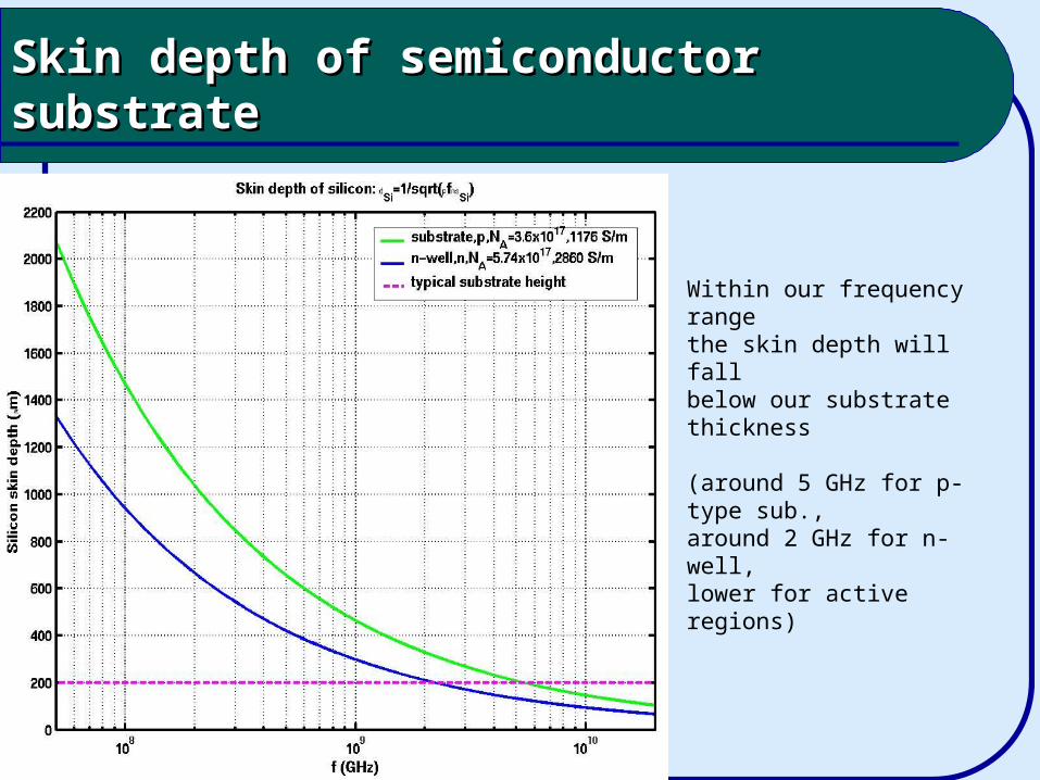
Skin depth of semiconductor Skin depth of semiconductor substratesubstrate
Within our frequency range the skin depth will fall below our substrate thickness
(around 5 GHz for p-type sub.,around 2 GHz for n-well, lower for active regions)
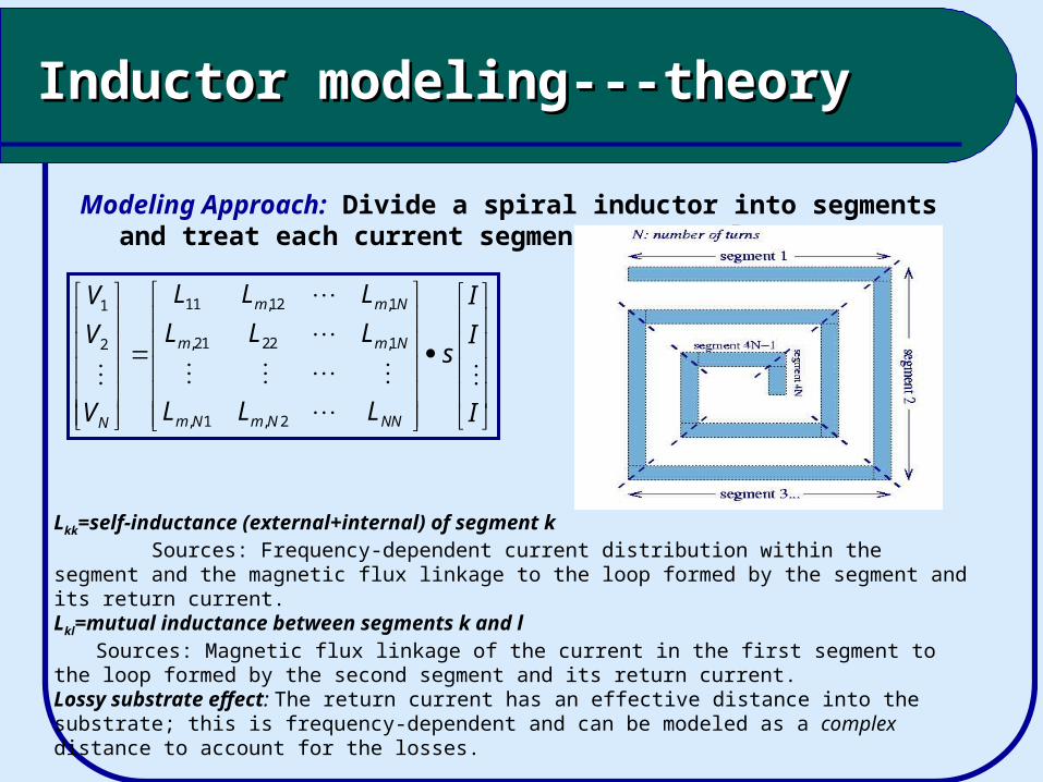
Inductor modeling---theoryInductor modeling---theory
Modeling Approach: Divide a spiral inductor into segments and treat each current segment separately.
11 ,12 ,11
,21 22 ,12
, 1 , 2
m m N
m m N
m N m N NNN
L L LV I
L L LV Is
L L LV I
Lkk=self-inductance (external+internal) of segment k Sources: Frequency-dependent current distribution within the segment and the magnetic flux linkage to the loop formed by the segment and its return current. Lkl=mutual inductance between segments k and l Sources: Magnetic flux linkage of the current in the first segment to the loop formed by the second segment and its return current.Lossy substrate effect: The return current has an effective distance into the substrate; this is frequency-dependent and can be modeled as a complex distance to account for the losses.
Other frequency dependency: Skin effect in the metal; current crowding in the metal
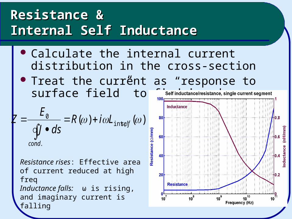
Resistance & Resistance & Internal Self Inductance Internal Self Inductance
Calculate the internal current distribution in the cross-section
Treat the current as “response to surface field” to find impedance
)()( int,
.
0 self
cond
LiRdsJ
EZ
Resistance rises: Effective area of current reduced at high freqInductance falls: ω is rising, and imaginary current is falling
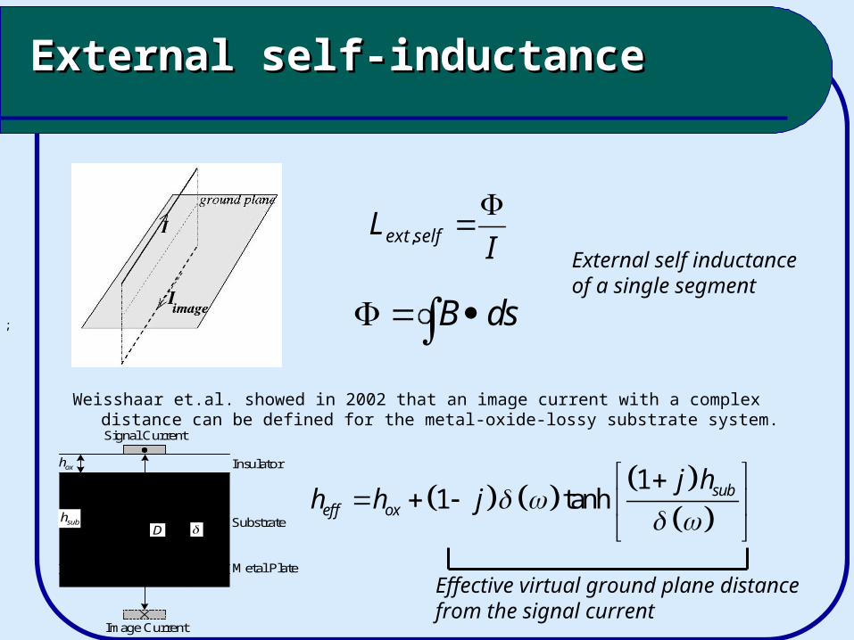
External self-inductanceExternal self-inductance
;
Weisshaar et.al. showed in 2002 that an image current with a complex distance can be defined for the metal-oxide-lossy substrate system.
11 tanh sub
eff ox
j hh h j
D
Insulatoroxh
Metal Plate
subh Substrate
Signal Current
Image Current
Effective virtual ground plane distancefrom the signal current
IL selfext
,
sdB
External self inductanceof a single segment
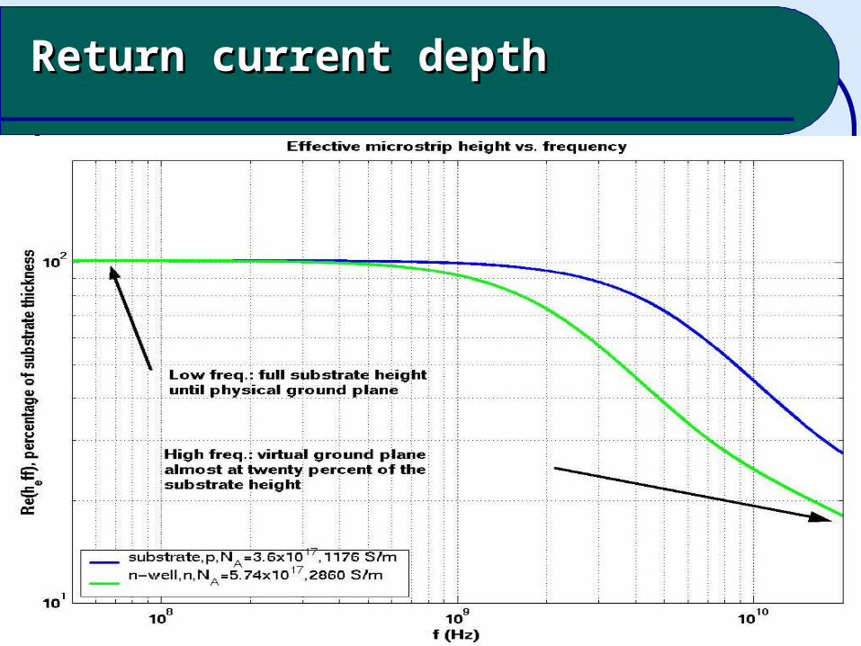
Return current depthReturn current depth
Mutual inductanceMutual inductance
,
14
i j
i i j j
j
c c j i ji ja b a b
i ijm ij
j j
a
J dl dlda da
a RL
J da
������������� �
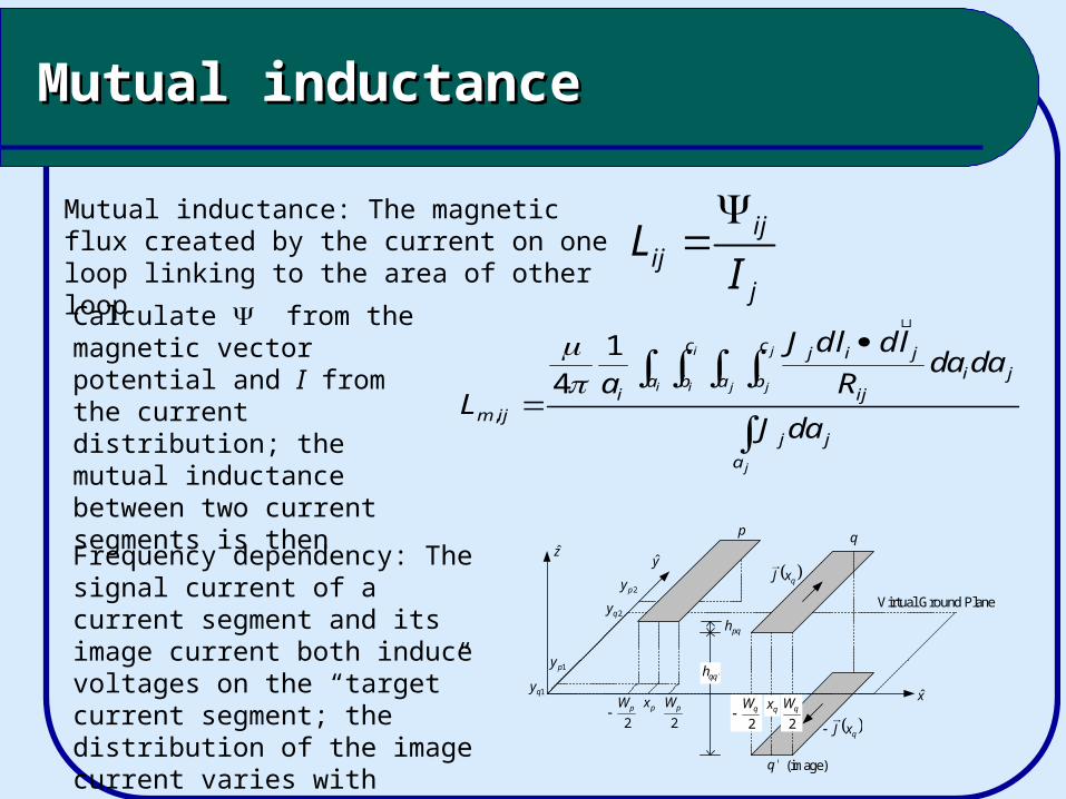
Mutual inductance: The magnetic flux created by the current on one loop linking to the area of other loop
ijij
j
LI
Calculate from the magnetic vector potential and I from the current distribution; the mutual inductance between two current segments is then
Frequency dependency: The signal current of a current segment and its image current both induce voltages on the “target” current segment; the distribution of the image current varies with frequency on a semiconductor substrate.
xpx qx
2pW
2pW
2qW
2qW
qxJ
qxJ
'qqh
yz
Virtual Ground Plane
qp
'q (image)
1py
2py
1qy
2qy
pqh
On-Chip Inductor ModelingOn-Chip Inductor Modeling
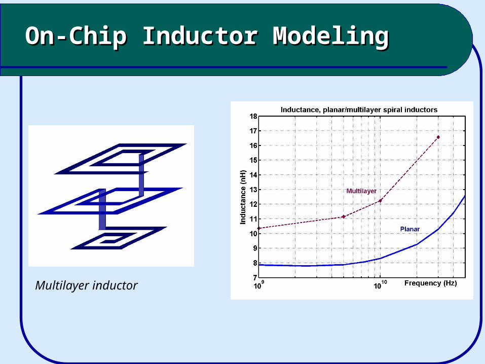
Multilayer inductor
Inductor modeling---Design Inductor modeling---Design issuesissues
Variations in layout: Metal layer Length Number of turns Metal trace width Metal trace spacing Substrate doping Shape …
Some ResultsSome Results
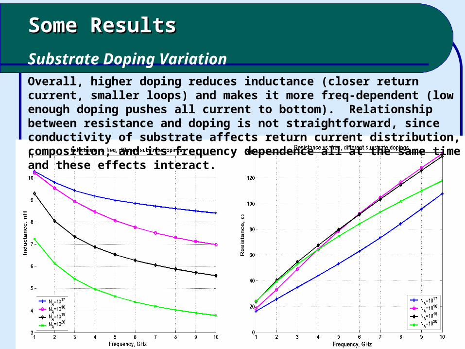
Substrate Doping VariationOverall, higher doping reduces inductance (closer return current, smaller loops) and makes it more freq-dependent (low enough doping pushes all current to bottom). Relationship between resistance and doping is not straightforward, since conductivity of substrate affects return current distribution, composition, and its frequency dependence all at the same time and these effects interact.

Inductors--- Test ChipsInductors--- Test Chips
Designed for RF-probe station measurements
Manufactured through MOSIS
AMIS 0.5 μm; 3 Metal layers
Structures on chip 1:
1. Planar inductor on grounded poly
2. Planar inductor on n-well3. Planar inductor on p-
substrate4. Planar inductor on n-plus5. De-embedding structure:
Open
1 2 3
4 5
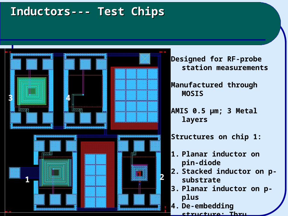
Inductors--- Test ChipsInductors--- Test Chips
Designed for RF-probe station measurements
Manufactured through MOSIS
AMIS 0.5 μm; 3 Metal layers
Structures on chip 1:
1. Planar inductor on pin-diode 2. Stacked inductor on p-
substrate3. Planar inductor on p-plus4. De-embedding structure:
Thru1 2
3 4
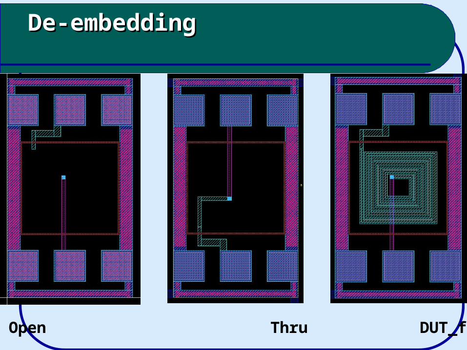
De-embeddingDe-embedding
Open Thru DUT_full
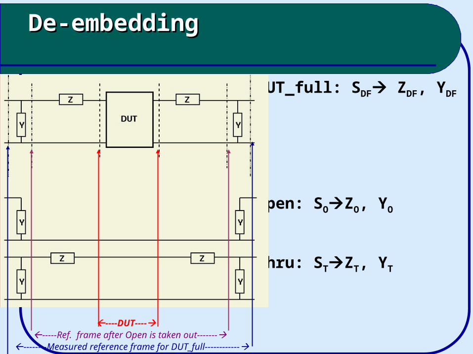
De-embeddingDe-embedding
DUT_full: SDF ZDF, YDF
Open: SOZO, YO
Thru: STZT, YT
--------Measured reference frame for DUT_full-----------------Ref. frame after Open is taken out-------
----DUT----
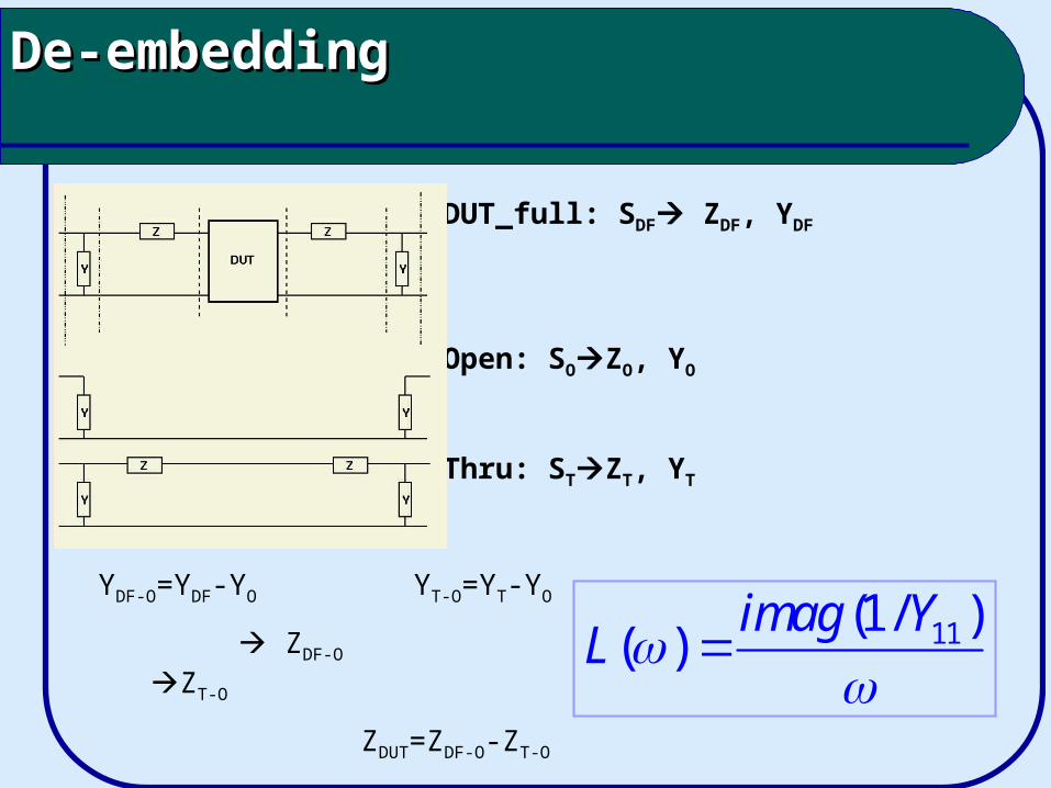
De-embeddingDe-embedding
DUT_full: SDF ZDF, YDF
Open: SOZO, YO
Thru: STZT, YT
YDF-O=YDF-YO YT-O=YT-YO
ZDF-O ZT-O
ZDUT=ZDF-O-ZT-O
YDUT, SDUT
11(1/ )( )
imag YL
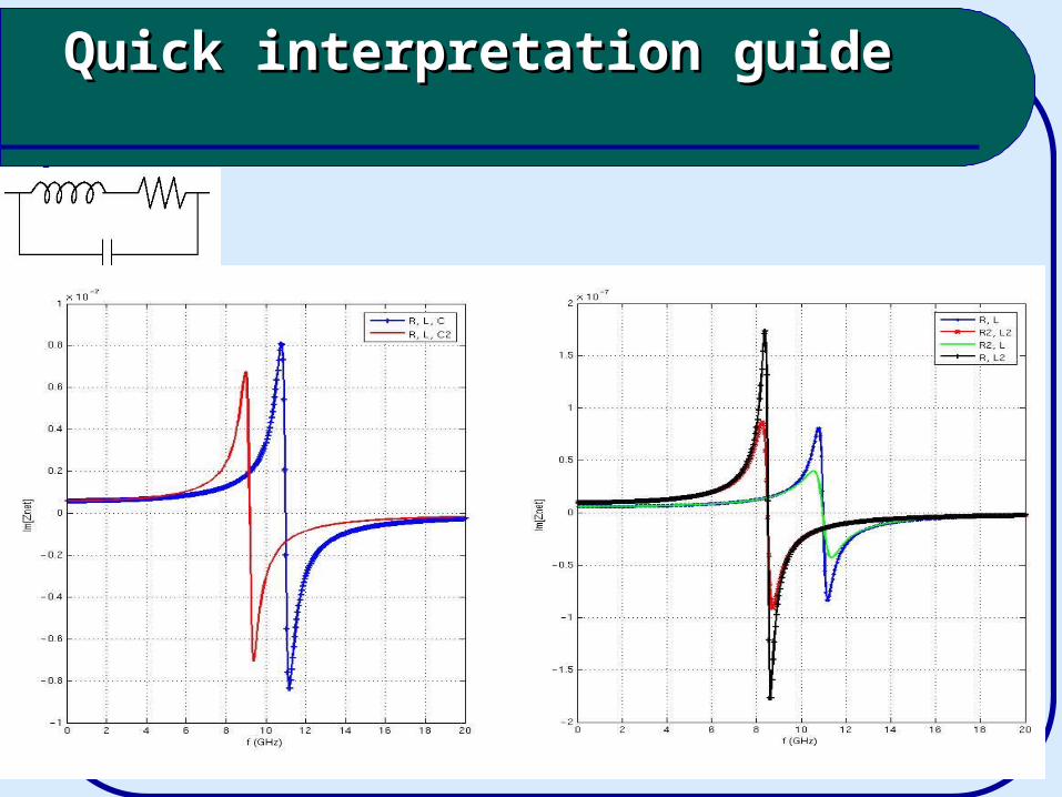
Quick interpretation guideQuick interpretation guide
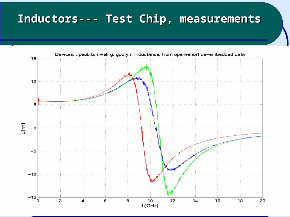
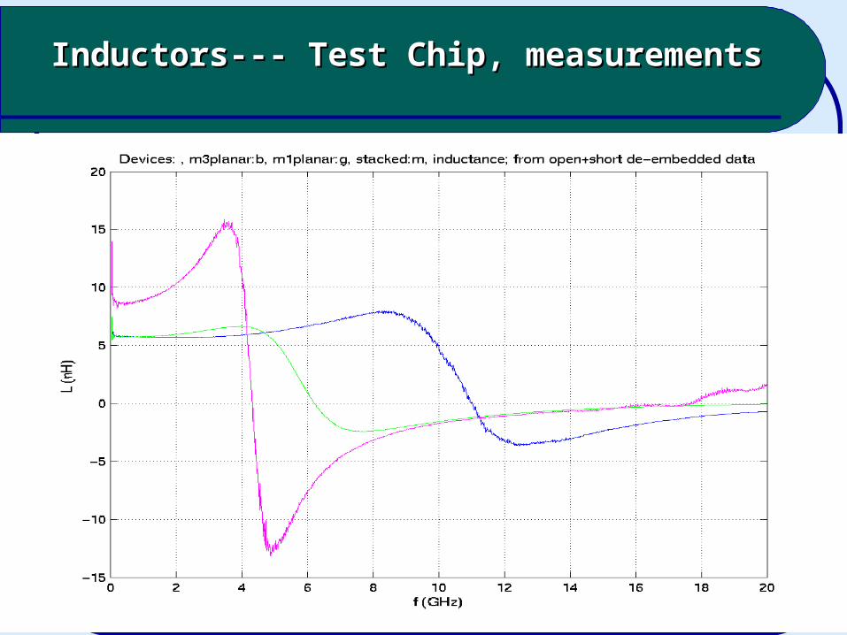
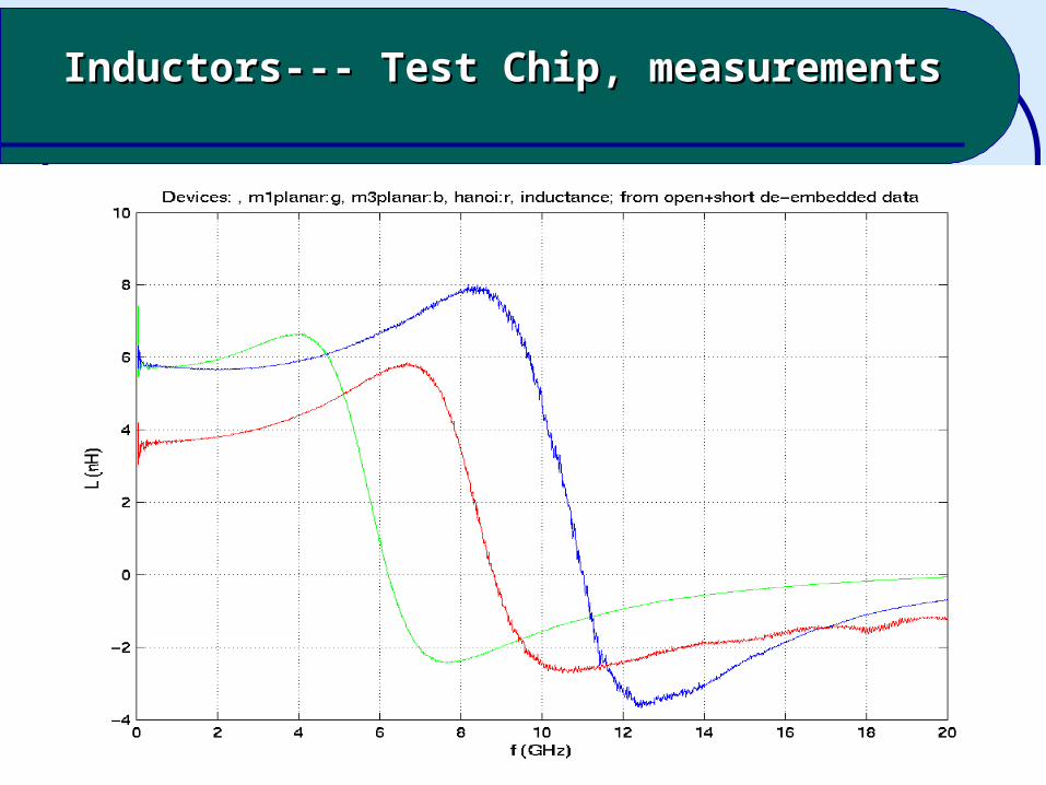
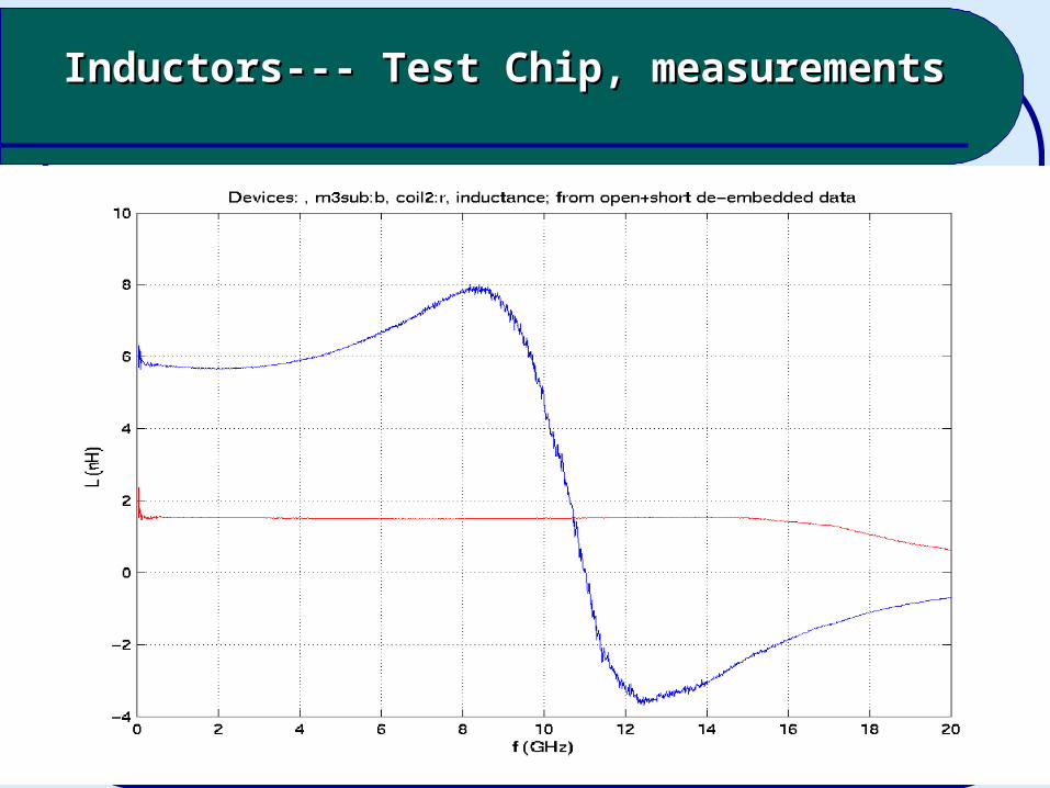
Inductors--- Test Chip, measurements Inductors--- Test Chip, measurements
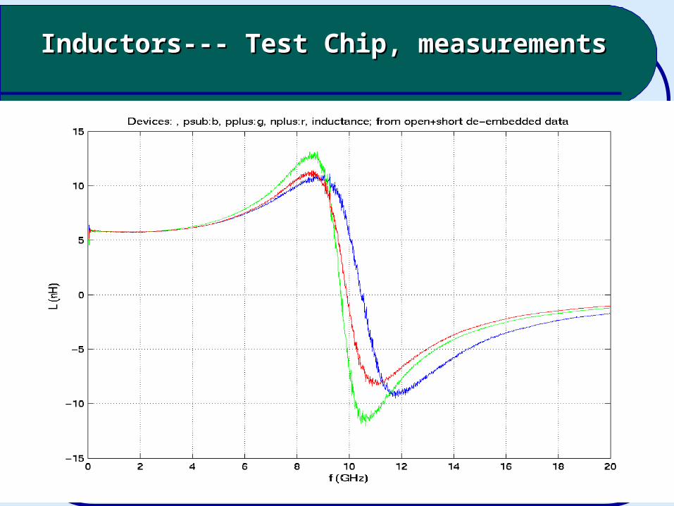
Inductors--- Test Chip, measurements Inductors--- Test Chip, measurements
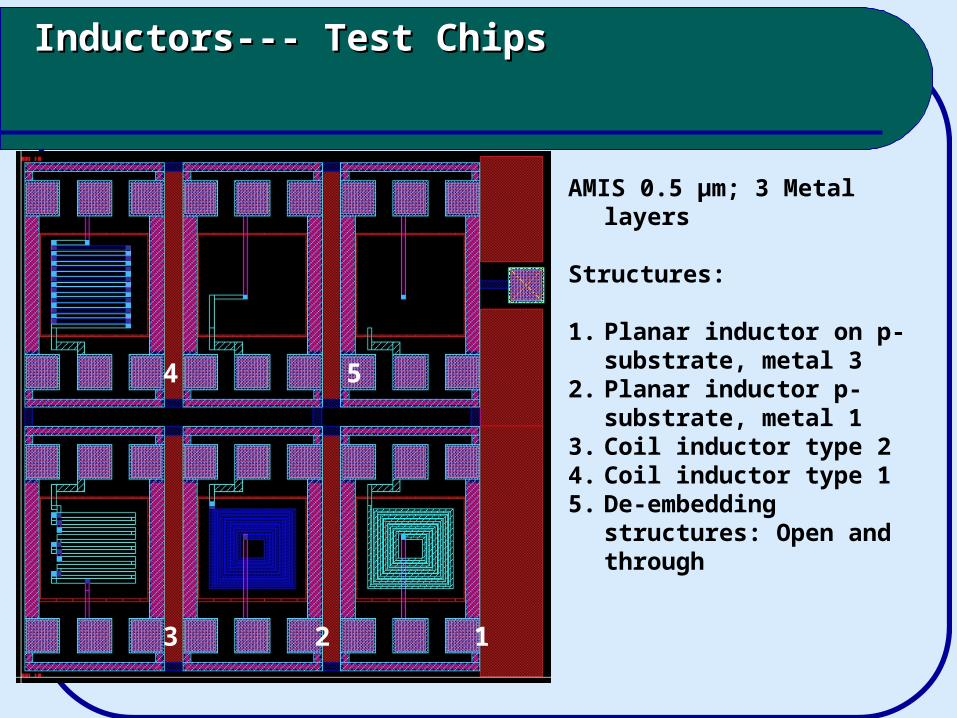
Inductors--- Test ChipsInductors--- Test Chips
123
4 5
AMIS 0.5 μm; 3 Metal layers
Structures:
1. Planar inductor on p-substrate, metal 3
2. Planar inductor p-substrate, metal 1
3. Coil inductor type 24. Coil inductor type 15. De-embedding structures:
Open and through
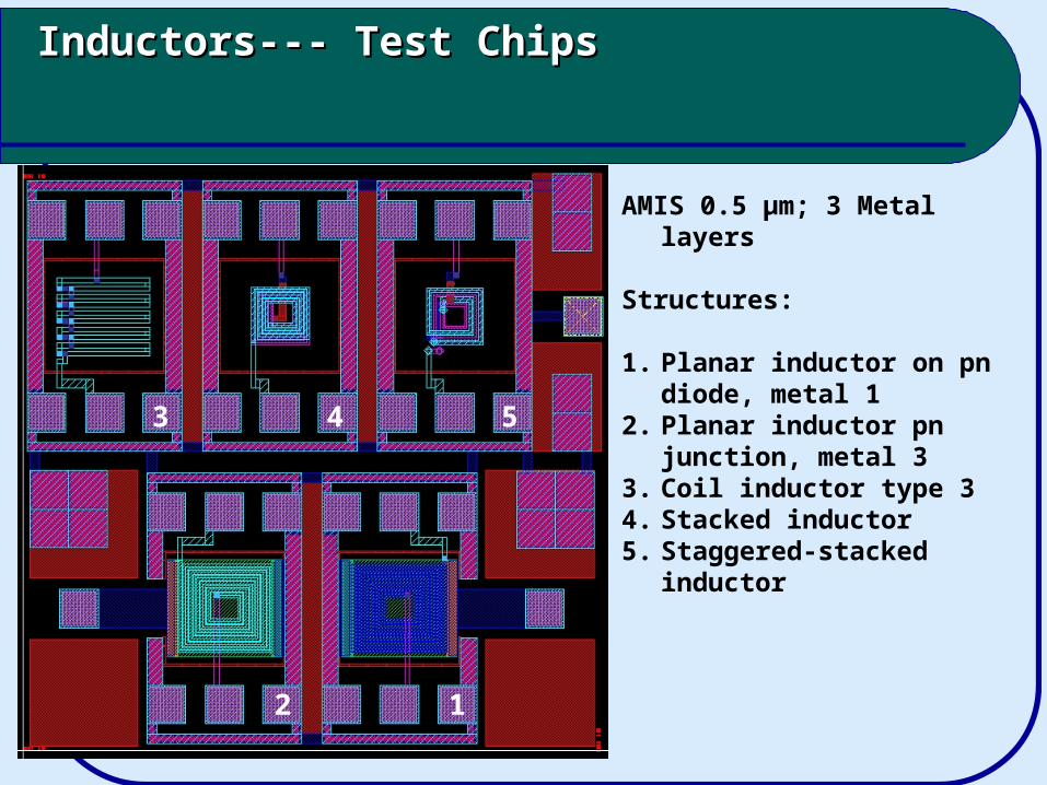
Inductors--- Test ChipsInductors--- Test Chips
AMIS 0.5 μm; 3 Metal layers
Structures:
1. Planar inductor on pn diode, metal 1
2. Planar inductor pn junction, metal 3
3. Coil inductor type 34. Stacked inductor5. Staggered-stacked inductor
12
3 4 5
Inductors--- Test Chip, measurements Inductors--- Test Chip, measurements
Inductors--- Test Chip, measurements Inductors--- Test Chip, measurements
Inductors--- Test Chip, measurements Inductors--- Test Chip, measurements
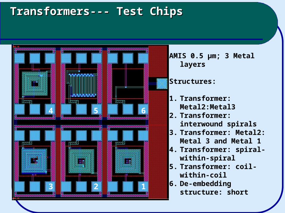
Transformers--- Test ChipsTransformers--- Test Chips
AMIS 0.5 μm; 3 Metal layers
Structures:
1. Transformer: Metal2:Metal32. Transformer: interwound
spirals3. Transformer: Metal2: Metal 3
and Metal 14. Transformer: spiral-within-
spiral5. Transformer: coil-within-coil6. De-embedding structure:
short
123
4 5 6