nemi optoelectronic substrates project (status report)...
TRANSCRIPT
NEMI OptoelectronicSubstrates
Project(Status Report)
Jack Fisher - Project Leader

The optoelectronics industry is moving at a rapid pace and new ideas and processes occur almost every week. The printed wiring board is one of the components that may impact or be impacted by the optoelectronic momentum. To enable the optoelectronic industry to meet it’s cost and performance targets the PWB must be able to carry both electrons and photons in the same substrate. The NEMI Optoelectronic Substrate team will investigate the use of optical waveguides in or on PWB’s.
Initial investigation by the committee determined that the OEM’s were not planning to use optoelectronics in their next generation machines.
The OEM’s felt that optoelectronics was at least two generations away from implementation in product that effect the revenue stream
The OEM’s were all working on internal analysis's of optoelectronic solutions and were all interested in participating in a NEMI technology analysis activity.
There are numerous estimates of how far copper can be pushed to increase data rates. The estimates range from 2.5 Gb/s to 40 Gb/s.
NEMI NationalNationalElectronicsElectronicsManufacturingManufacturingInitiative, Inc.Initiative, Inc. Inititatives
Cost/performance modeling of optical wave guides vs. copper conductors Inititative
Objective:Develop a cost model for a “copper” telecom industry backplane and then model potential designs for equivalent optoelectronic backplanes. The goal is to determine a bandwidth crossover point between copper and opto. Currently the team is using a backplane as the primary focus of the activity. Copper and optoelectronic transmitters and receivers may also need to be included which also may allow an analysis of chip carrier technology to be included in the project.
Activities:In light of the OEM’s not booking optoelectronics as part of their next generation equipment it was decided to do a business analysis of copper vs. optoelectronics
The product to be analyzed will be a communications industry backplane.
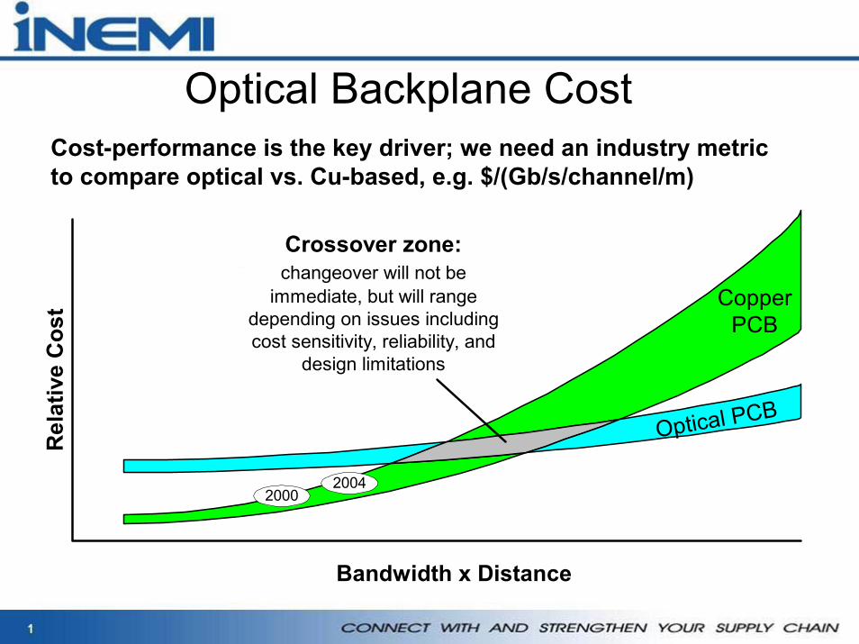
Optical Backplane CostCost-performance is the key driver; we need an industry metricto compare optical vs. Cu-based, e.g. $/(Gb/s/channel/m)
Crossover zone:changeover will not be
immediate, but will rangedepending on issues includingcost sensitivity, reliability, and
design limitations
Bandwidth x Distance
Rel
ativ
e C
ost Copper
PCB
Optical PCB
20042000
• Jack Fisher• Bruce Booth

Status:•Bi-monthly telecons•Very good participation
•Several OEM’s•Several fabricators / Contract assemblers•Several material suppliers
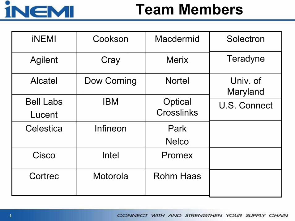
Team Members
Rohm HaasMotorolaCortrec
PromexIntelCisco
ParkNelco
InfineonCelestica
Optical Crosslinks
IBMBell LabsLucent
NortelDow CorningAlcatel
MerixCrayAgilent
MacdermidCooksoniNEMI
U.S. Connect
Univ. of Maryland
Teradyne
Solectron
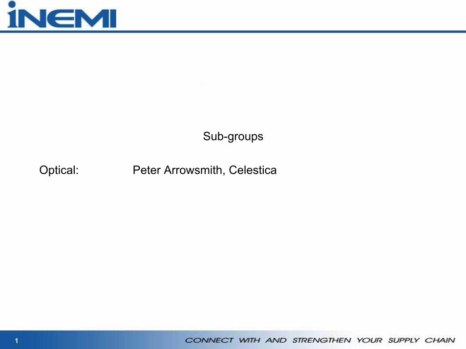
Sub-groups
Optical: Peter Arrowsmith, Celestica

• To do a business model you need:
• A modeling tool• PCB cost model• Component assembly model tool
• Select optoelectronic technology alternatives• Fiber• Waveguide• Polymer appliqué• Etc
•Develop and agree on sensitivities (materials,components, process, etc.)
•Opto sensitivities•Copper sensitivities
•Develop and agree on architectures•Opto architectures•Copper architectures
Difficult because it is often proprietary information
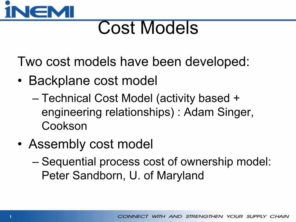
Cost Models
Two cost models have been developed:• Backplane cost model
– Technical Cost Model (activity based + engineering relationships) : Adam Singer, Cookson
• Assembly cost model– Sequential process cost of ownership model:
Peter Sandborn, U. of Maryland
Assembly Cost Modeling Approach
• Sequential process model – the sequence of process steps is important because modeling recurring functional test (and possibly rework is important)
• Supports system physical hierarchical – parts -> subassemblies -> assemblies, etc.
• Distinguishes between mature and immature processes and parts
• Relative costs – more interested in accurately modeling cost differences between technology options rather than absolute costs

Assembly Cost Modeling Inputs
• Part data– Procurement cost and yield at assembly
• Assembly process data– Generic processing steps with labor, material,
tooling, and capital equipment contributions– Recurring functional test steps (additionally
characterized by fault coverage)– Rework steps

Assembly Cost Model
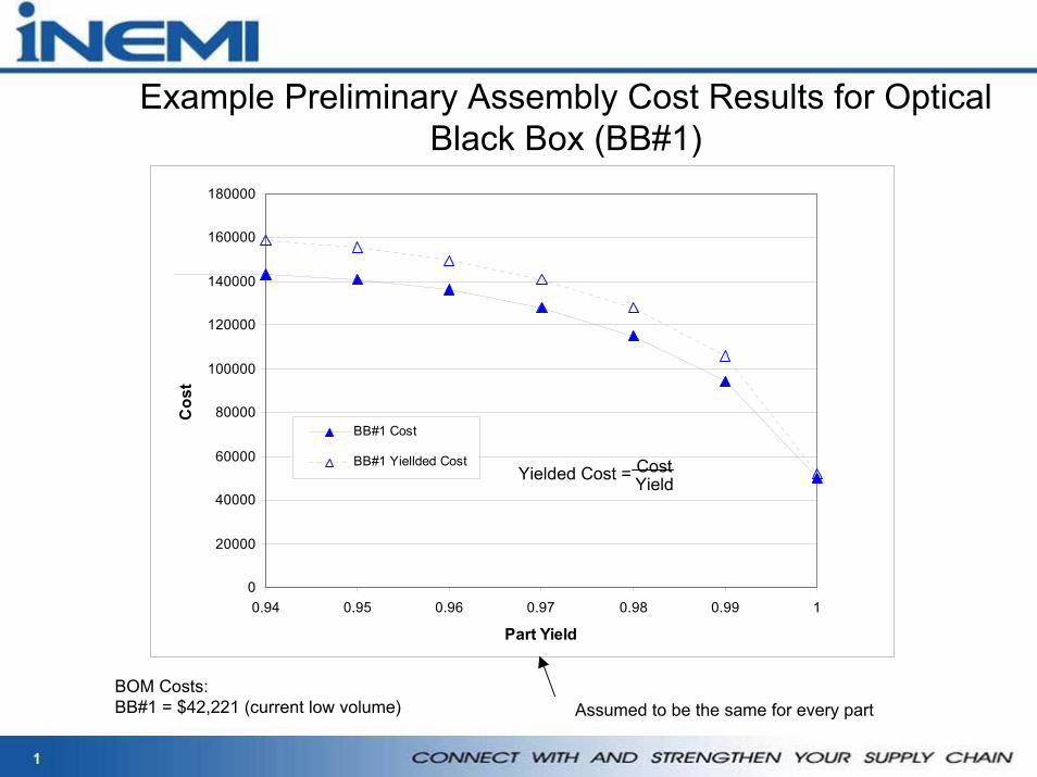
Example Preliminary Assembly Cost Results for Optical Black Box (BB#1)
0
20000
40000
60000
80000
100000
120000
140000
160000
180000
0.94 0.95 0.96 0.97 0.98 0.99 1
Part Yield
Cos
t
BB#1 Cost
BB#1 Yiellded CostYielded Cost = Cost
Yield
BOM Costs:BB#1 = $42,221 (current low volume) Assumed to be the same for every part
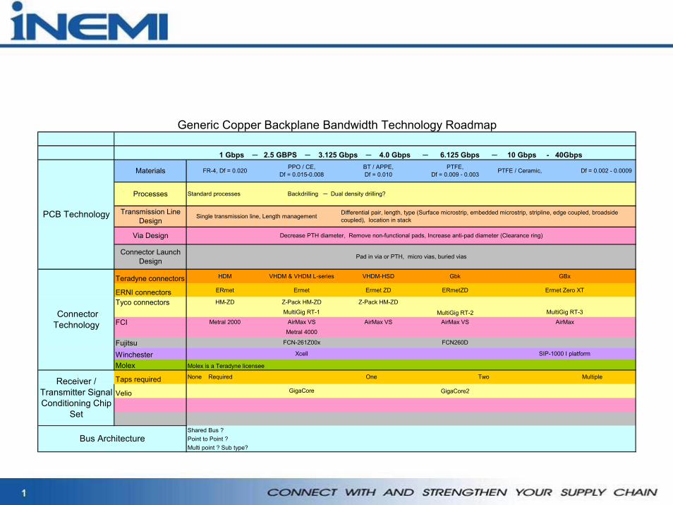
Teradyne connectors HDM VHDM & VHDM L-series VHDM-HSD Gbk GBx
ERNI connectors ERmet Ermet Ermet ZD ERmetZD Ermet Zero XT
Tyco connectors HM-ZD Z-Pack HM-ZD Z-Pack HM-ZD
MultiGig RT-1 MultiGig RT-2 MultiGig RT-3
FCI Metral 2000 AirMax VS AirMax VS AirMax VS AirMax
Metral 4000
Fujitsu FCN-261Z00x FCN260D
Winchester Xcell SIP-1000 I platform
Molex Molex is a Teradyne licensee
Taps required
Velio GigaCore2
Shared Bus ?Point to Point ?Multi point ? Sub type?
Generic Copper Backplane Bandwidth Technology Roadmap
PTFE / Ceramic, Df = 0.002 - 0.0009FR-4, Df = 0.020 PPO / CE, Df = 0.015-0.008
BT / APPE, Df = 0.010
PTFE, Df = 0.009 - 0.003
1 Gbps ─ 2.5 GBPS ─ 3.125 Gbps ─ 4.0 Gbps ─ 6.125 Gbps ─ 10 Gbps - 40Gbps
Materials
PCB Technology
Connector Launch Design
Transmission Line Design
Differential pair, length, type (Surface microstrip, embedded microstrip, stripline, edge coupled, broadside coupled), location in stack Single transmission line, Length management
Processes Standard processes Backdrilling ─ Dual density drilling?
Bus Architecture
Receiver / Transmitter Signal Conditioning Chip
Set
Pad in via or PTH, micro vias, buried vias
Decrease PTH diameter, Remove non-functional pads, Increase anti-pad diameter (Clearance ring)
Connector Technology
Via Design
GigaCore
None Required One Two Multiple

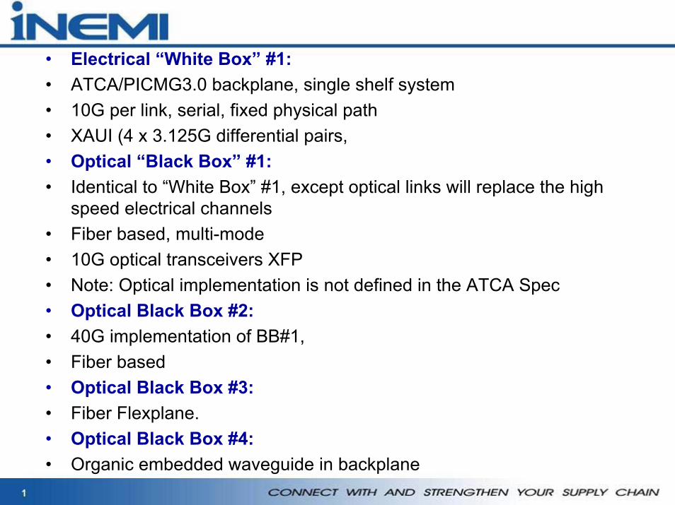
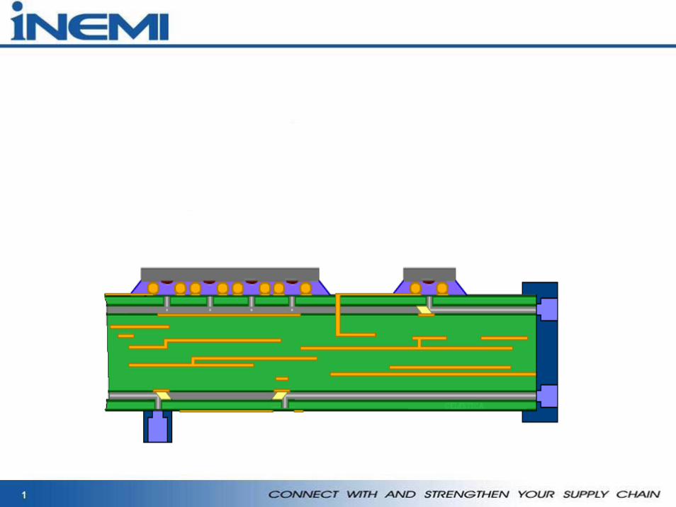
• Electrical “White Box” #1:• ATCA/PICMG3.0 backplane, single shelf system• 10G per link, serial, fixed physical path• XAUI (4 x 3.125G differential pairs, • Optical “Black Box” #1:• Identical to “White Box” #1, except optical links will replace the high
speed electrical channels• Fiber based, multi-mode• 10G optical transceivers XFP • Note: Optical implementation is not defined in the ATCA Spec• Optical Black Box #2:• 40G implementation of BB#1, • Fiber based• Optical Black Box #3:• Fiber Flexplane.• Optical Black Box #4:• Organic embedded waveguide in backplane